EP2605276A2 - Packaged leadless semiconductor device - Google Patents
Packaged leadless semiconductor device Download PDFInfo
- Publication number
- EP2605276A2 EP2605276A2 EP12194468.0A EP12194468A EP2605276A2 EP 2605276 A2 EP2605276 A2 EP 2605276A2 EP 12194468 A EP12194468 A EP 12194468A EP 2605276 A2 EP2605276 A2 EP 2605276A2
- Authority
- EP
- European Patent Office
- Prior art keywords
- heat sink
- flange
- semiconductor device
- sink flange
- terminal pads
- Prior art date
- Legal status (The legal status is an assumption and is not a legal conclusion. Google has not performed a legal analysis and makes no representation as to the accuracy of the status listed.)
- Granted
Links
Images



Classifications
-
- H—ELECTRICITY
- H10—SEMICONDUCTOR DEVICES; ELECTRIC SOLID-STATE DEVICES NOT OTHERWISE PROVIDED FOR
- H10W—GENERIC PACKAGES, INTERCONNECTIONS, CONNECTORS OR OTHER CONSTRUCTIONAL DETAILS OF DEVICES COVERED BY CLASS H10
- H10W74/00—Encapsulations, e.g. protective coatings
- H10W74/01—Manufacture or treatment
-
- H—ELECTRICITY
- H10—SEMICONDUCTOR DEVICES; ELECTRIC SOLID-STATE DEVICES NOT OTHERWISE PROVIDED FOR
- H10W—GENERIC PACKAGES, INTERCONNECTIONS, CONNECTORS OR OTHER CONSTRUCTIONAL DETAILS OF DEVICES COVERED BY CLASS H10
- H10W20/00—Interconnections in chips, wafers or substrates
- H10W20/01—Manufacture or treatment
- H10W20/031—Manufacture or treatment of conductive parts of the interconnections
- H10W20/0698—Local interconnections
-
- H—ELECTRICITY
- H10—SEMICONDUCTOR DEVICES; ELECTRIC SOLID-STATE DEVICES NOT OTHERWISE PROVIDED FOR
- H10W—GENERIC PACKAGES, INTERCONNECTIONS, CONNECTORS OR OTHER CONSTRUCTIONAL DETAILS OF DEVICES COVERED BY CLASS H10
- H10W40/00—Arrangements for thermal protection or thermal control
- H10W40/20—Arrangements for cooling
- H10W40/22—Arrangements for cooling characterised by their shape, e.g. having conical or cylindrical projections
-
- H—ELECTRICITY
- H10—SEMICONDUCTOR DEVICES; ELECTRIC SOLID-STATE DEVICES NOT OTHERWISE PROVIDED FOR
- H10W—GENERIC PACKAGES, INTERCONNECTIONS, CONNECTORS OR OTHER CONSTRUCTIONAL DETAILS OF DEVICES COVERED BY CLASS H10
- H10W40/00—Arrangements for thermal protection or thermal control
- H10W40/70—Fillings or auxiliary members in containers or in encapsulations for thermal protection or control
- H10W40/77—Auxiliary members characterised by their shape
- H10W40/778—Auxiliary members characterised by their shape in encapsulations
-
- H—ELECTRICITY
- H10—SEMICONDUCTOR DEVICES; ELECTRIC SOLID-STATE DEVICES NOT OTHERWISE PROVIDED FOR
- H10W—GENERIC PACKAGES, INTERCONNECTIONS, CONNECTORS OR OTHER CONSTRUCTIONAL DETAILS OF DEVICES COVERED BY CLASS H10
- H10W70/00—Package substrates; Interposers; Redistribution layers [RDL]
- H10W70/40—Leadframes
- H10W70/421—Shapes or dispositions
-
- H—ELECTRICITY
- H10—SEMICONDUCTOR DEVICES; ELECTRIC SOLID-STATE DEVICES NOT OTHERWISE PROVIDED FOR
- H10W—GENERIC PACKAGES, INTERCONNECTIONS, CONNECTORS OR OTHER CONSTRUCTIONAL DETAILS OF DEVICES COVERED BY CLASS H10
- H10W70/00—Package substrates; Interposers; Redistribution layers [RDL]
- H10W70/40—Leadframes
- H10W70/421—Shapes or dispositions
- H10W70/424—Cross-sectional shapes
- H10W70/427—Bent parts
-
- H—ELECTRICITY
- H10—SEMICONDUCTOR DEVICES; ELECTRIC SOLID-STATE DEVICES NOT OTHERWISE PROVIDED FOR
- H10W—GENERIC PACKAGES, INTERCONNECTIONS, CONNECTORS OR OTHER CONSTRUCTIONAL DETAILS OF DEVICES COVERED BY CLASS H10
- H10W70/00—Package substrates; Interposers; Redistribution layers [RDL]
- H10W70/40—Leadframes
- H10W70/464—Additional interconnections in combination with leadframes
- H10W70/465—Bumps or wires
-
- H—ELECTRICITY
- H10—SEMICONDUCTOR DEVICES; ELECTRIC SOLID-STATE DEVICES NOT OTHERWISE PROVIDED FOR
- H10W—GENERIC PACKAGES, INTERCONNECTIONS, CONNECTORS OR OTHER CONSTRUCTIONAL DETAILS OF DEVICES COVERED BY CLASS H10
- H10W72/00—Interconnections or connectors in packages
- H10W72/01—Manufacture or treatment
- H10W72/0198—Manufacture or treatment batch processes
-
- H—ELECTRICITY
- H10—SEMICONDUCTOR DEVICES; ELECTRIC SOLID-STATE DEVICES NOT OTHERWISE PROVIDED FOR
- H10W—GENERIC PACKAGES, INTERCONNECTIONS, CONNECTORS OR OTHER CONSTRUCTIONAL DETAILS OF DEVICES COVERED BY CLASS H10
- H10W72/00—Interconnections or connectors in packages
- H10W72/071—Connecting or disconnecting
- H10W72/075—Connecting or disconnecting of bond wires
-
- H—ELECTRICITY
- H10—SEMICONDUCTOR DEVICES; ELECTRIC SOLID-STATE DEVICES NOT OTHERWISE PROVIDED FOR
- H10W—GENERIC PACKAGES, INTERCONNECTIONS, CONNECTORS OR OTHER CONSTRUCTIONAL DETAILS OF DEVICES COVERED BY CLASS H10
- H10W72/00—Interconnections or connectors in packages
- H10W72/071—Connecting or disconnecting
- H10W72/075—Connecting or disconnecting of bond wires
- H10W72/07551—Connecting or disconnecting of bond wires characterised by changes in properties of the bond wires during the connecting
- H10W72/07554—Connecting or disconnecting of bond wires characterised by changes in properties of the bond wires during the connecting changes in dispositions
-
- H—ELECTRICITY
- H10—SEMICONDUCTOR DEVICES; ELECTRIC SOLID-STATE DEVICES NOT OTHERWISE PROVIDED FOR
- H10W—GENERIC PACKAGES, INTERCONNECTIONS, CONNECTORS OR OTHER CONSTRUCTIONAL DETAILS OF DEVICES COVERED BY CLASS H10
- H10W72/00—Interconnections or connectors in packages
- H10W72/50—Bond wires
- H10W72/531—Shapes of wire connectors
- H10W72/533—Cross-sectional shape
- H10W72/534—Cross-sectional shape being rectangular
-
- H—ELECTRICITY
- H10—SEMICONDUCTOR DEVICES; ELECTRIC SOLID-STATE DEVICES NOT OTHERWISE PROVIDED FOR
- H10W—GENERIC PACKAGES, INTERCONNECTIONS, CONNECTORS OR OTHER CONSTRUCTIONAL DETAILS OF DEVICES COVERED BY CLASS H10
- H10W72/00—Interconnections or connectors in packages
- H10W72/50—Bond wires
- H10W72/531—Shapes of wire connectors
- H10W72/5366—Shapes of wire connectors the bond wires having kinks
-
- H—ELECTRICITY
- H10—SEMICONDUCTOR DEVICES; ELECTRIC SOLID-STATE DEVICES NOT OTHERWISE PROVIDED FOR
- H10W—GENERIC PACKAGES, INTERCONNECTIONS, CONNECTORS OR OTHER CONSTRUCTIONAL DETAILS OF DEVICES COVERED BY CLASS H10
- H10W72/00—Interconnections or connectors in packages
- H10W72/50—Bond wires
- H10W72/541—Dispositions of bond wires
- H10W72/5445—Dispositions of bond wires being orthogonal to a side surface of the chip, e.g. parallel arrangements
-
- H—ELECTRICITY
- H10—SEMICONDUCTOR DEVICES; ELECTRIC SOLID-STATE DEVICES NOT OTHERWISE PROVIDED FOR
- H10W—GENERIC PACKAGES, INTERCONNECTIONS, CONNECTORS OR OTHER CONSTRUCTIONAL DETAILS OF DEVICES COVERED BY CLASS H10
- H10W72/00—Interconnections or connectors in packages
- H10W72/50—Bond wires
- H10W72/551—Materials of bond wires
- H10W72/552—Materials of bond wires comprising metals or metalloids, e.g. silver
- H10W72/5522—Materials of bond wires comprising metals or metalloids, e.g. silver comprising gold [Au]
-
- H—ELECTRICITY
- H10—SEMICONDUCTOR DEVICES; ELECTRIC SOLID-STATE DEVICES NOT OTHERWISE PROVIDED FOR
- H10W—GENERIC PACKAGES, INTERCONNECTIONS, CONNECTORS OR OTHER CONSTRUCTIONAL DETAILS OF DEVICES COVERED BY CLASS H10
- H10W72/00—Interconnections or connectors in packages
- H10W72/50—Bond wires
- H10W72/551—Materials of bond wires
- H10W72/552—Materials of bond wires comprising metals or metalloids, e.g. silver
- H10W72/5524—Materials of bond wires comprising metals or metalloids, e.g. silver comprising aluminium [Al]
-
- H—ELECTRICITY
- H10—SEMICONDUCTOR DEVICES; ELECTRIC SOLID-STATE DEVICES NOT OTHERWISE PROVIDED FOR
- H10W—GENERIC PACKAGES, INTERCONNECTIONS, CONNECTORS OR OTHER CONSTRUCTIONAL DETAILS OF DEVICES COVERED BY CLASS H10
- H10W72/00—Interconnections or connectors in packages
- H10W72/90—Bond pads, in general
- H10W72/951—Materials of bond pads
-
- H—ELECTRICITY
- H10—SEMICONDUCTOR DEVICES; ELECTRIC SOLID-STATE DEVICES NOT OTHERWISE PROVIDED FOR
- H10W—GENERIC PACKAGES, INTERCONNECTIONS, CONNECTORS OR OTHER CONSTRUCTIONAL DETAILS OF DEVICES COVERED BY CLASS H10
- H10W74/00—Encapsulations, e.g. protective coatings
-
- H—ELECTRICITY
- H10—SEMICONDUCTOR DEVICES; ELECTRIC SOLID-STATE DEVICES NOT OTHERWISE PROVIDED FOR
- H10W—GENERIC PACKAGES, INTERCONNECTIONS, CONNECTORS OR OTHER CONSTRUCTIONAL DETAILS OF DEVICES COVERED BY CLASS H10
- H10W74/00—Encapsulations, e.g. protective coatings
- H10W74/10—Encapsulations, e.g. protective coatings characterised by their shape or disposition
- H10W74/111—Encapsulations, e.g. protective coatings characterised by their shape or disposition the semiconductor body being completely enclosed
-
- H—ELECTRICITY
- H10—SEMICONDUCTOR DEVICES; ELECTRIC SOLID-STATE DEVICES NOT OTHERWISE PROVIDED FOR
- H10W—GENERIC PACKAGES, INTERCONNECTIONS, CONNECTORS OR OTHER CONSTRUCTIONAL DETAILS OF DEVICES COVERED BY CLASS H10
- H10W90/00—Package configurations
- H10W90/701—Package configurations characterised by the relative positions of pads or connectors relative to package parts
- H10W90/751—Package configurations characterised by the relative positions of pads or connectors relative to package parts of bond wires
- H10W90/753—Package configurations characterised by the relative positions of pads or connectors relative to package parts of bond wires between laterally-adjacent chips
-
- H—ELECTRICITY
- H10—SEMICONDUCTOR DEVICES; ELECTRIC SOLID-STATE DEVICES NOT OTHERWISE PROVIDED FOR
- H10W—GENERIC PACKAGES, INTERCONNECTIONS, CONNECTORS OR OTHER CONSTRUCTIONAL DETAILS OF DEVICES COVERED BY CLASS H10
- H10W90/00—Package configurations
- H10W90/701—Package configurations characterised by the relative positions of pads or connectors relative to package parts
- H10W90/751—Package configurations characterised by the relative positions of pads or connectors relative to package parts of bond wires
- H10W90/755—Package configurations characterised by the relative positions of pads or connectors relative to package parts of bond wires between a chip and a laterally-adjacent insulating package substrate, interpose or RDL
-
- H—ELECTRICITY
- H10—SEMICONDUCTOR DEVICES; ELECTRIC SOLID-STATE DEVICES NOT OTHERWISE PROVIDED FOR
- H10W—GENERIC PACKAGES, INTERCONNECTIONS, CONNECTORS OR OTHER CONSTRUCTIONAL DETAILS OF DEVICES COVERED BY CLASS H10
- H10W90/00—Package configurations
- H10W90/701—Package configurations characterised by the relative positions of pads or connectors relative to package parts
- H10W90/751—Package configurations characterised by the relative positions of pads or connectors relative to package parts of bond wires
- H10W90/756—Package configurations characterised by the relative positions of pads or connectors relative to package parts of bond wires between a chip and a stacked lead frame, conducting package substrate or heat sink
-
- H—ELECTRICITY
- H10—SEMICONDUCTOR DEVICES; ELECTRIC SOLID-STATE DEVICES NOT OTHERWISE PROVIDED FOR
- H10W—GENERIC PACKAGES, INTERCONNECTIONS, CONNECTORS OR OTHER CONSTRUCTIONAL DETAILS OF DEVICES COVERED BY CLASS H10
- H10W90/00—Package configurations
- H10W90/811—Multiple chips on leadframes
Definitions
- the present invention relates generally to semiconductor devices. More specifically, the present invention relates to leadless semiconductor devices.
- Semiconductor chips or dies are typically encapsulated in a semiconductor package for protection from damage by external stresses and to provide a system for carrying electrical signals to and from the chips.
- semiconductor packages exist including dual-in-line packages, pin grid array packages, tape-automated bonding (TAB) packages, multi-chip modules (MCMs), and power packages.
- TAB tape-automated bonding
- MCMs multi-chip modules
- power package is used for a high power semiconductor device that is capable of dissipating, for example, greater than thirty watts of power. Such a power package may be utilized in, for example, a radiofrequency application.
- FIG. 1 shows a top perspective view of a semiconductor device in accordance with an embodiment
- FIG. 2 shows a bottom perspective view of the semiconductor device of FIG. 1 ;
- FIG. 3 shows a cross-sectional view of the semiconductor device of FIG. 1 ;
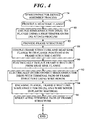
- FIG. 4 shows a flowchart of a semiconductor device assembly process in accordance with another embodiment
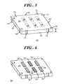
- FIG. 5 shows a perspective view of a heat sink flange of the semiconductor device provided at an initial stage of assembly in accordance with the assembly process of FIG. 4 ;
- FIG. 6 shows a perspective view of heat sink flange at a subsequent stage of assembly in accordance with the assembly process of FIG. 4 ;
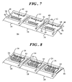
- FIG. 7 shows a perspective view of a frame structure panel for frame structure of the semiconductor device provided at a subsequent stage of assembly in accordance with the assembly process of FIG. 4 ;
- FIG. 8 shows a perspective view of the frame structure panel coupled with a number of heat sink flanges at a subsequent stage of assembly in accordance with the assembly process of FIG. 4 ;
- FIG. 9 shows an enlarged perspective view of the heat sink flange and the frame structure at a subsequent stage of assembly in accordance with the assembly process of FIG. 4 ;
- FIG. 10 shows a perspective view of the semiconductor devices at a subsequent stage of assembly in accordance with the assembly process of FIG. 4 ;
- FIG. 11 shows a perspective view of the heat sink flange and the frame structure in accordance with an alternative embodiment of the assembly process
- FIG. 12 shows a perspective view of a cap utilized in accordance with the alternative embodiment.
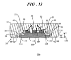
- FIG. 13 shows a cross-sectional view of a semiconductor device in accordance with another alternative embodiment.
- a leadframe typically includes a die flange or paddle and terminal pads surrounding the die flange.
- One or more semiconductor dies are attached using, for example, epoxy or high temperature solder to the die flange, and the terminal pads are electrically interconnected with the semiconductor die or dies using a wire bonding process. These terminal pads are formed coplanar with the device backside in order to make contact with an underlying printed circuit board when surface mounted.
- a high temperature metallurgical bonding process such as gold-silicon bonding, gold-tin bonding, silver bonding, and so forth.
- a high temperature bonding process is not a suitable for typical leadless surface mount packages containing multiple dies because the high temperature can cause warping of or otherwise damage the leadframe.
- Embodiments described herein entail a leadless semiconductor device for high power applications and an assembly process for packaging the leadless semiconductor device.
- the semiconductor device includes a relatively thick heat sink flange and a separate frame structure.
- the frame structure is pre-formed with bent terminal pads.
- the semiconductor dies can be attached to the heat sink flange using a high temperature die attach process.
- the frame structure can subsequently be combined with the heat sink flange so that the lower surface of the heat sink flange and a portion of the terminal pads are in coplanar alignment.
- the structure can then be encapsulated in an encapsulant (such as a plastic material) so that the lower surface of the heat sink flange and the terminal pads remain exposed from the encapsulant.
- an encapsulant such as a plastic material
- Such a technique facilitates packaging flexibility and achieves improvements in wire bond quality. Furthermore, flatness of the packaged semiconductor device and coplanarity of the elements is maintained due to the relatively thick heat sink flange. Accordingly, a lower package with enhanced performance and improved reliability can be achieved for high power radiofrequency applications.
- FIG. 1 shows a top perspective view of a semiconductor device 20 in accordance with an embodiment.
- FIG. 2 shows a bottom perspective view of semiconductor device 20, and
- FIG. 3 shows a cross-sectional view of semiconductor device 20.
- semiconductor device 20 includes a heat sink flange 24, one or more semiconductor dies 26, a frame structure 28, and bond wires 30.
- Semiconductor device 20 is a leadless surface mount package in which the components of semiconductor device 20 are substantially encased in an encapsulant 32, such as a molding compound encapsulant.
- a term “horizontal” may be used herein to define a plane parallel to the plane or surface of the semiconductor device 20, regardless of its orientation.
- a term “vertical” refers to a direction perpendicular to the horizontal as defmed. Terms, such as “above,” “below,” “top,” “bottom,” “side” (as in “sidewall”), "upper,” “lower,” and so forth are defined with respect to the horizontal plane.
- Heat sink flange 24 has an upper surface 34 and a lower surface 36 spaced apart from upper surface 34 by a flange thickness 38.
- Heat sink flange 24 may be thermally and electrically conductive copper or a copper laminate material.
- One or more semiconductor dies 26 are coupled to upper surface 34 of heat sink flange 24.
- semiconductor dies 26 may be high power, e.g., greater than thirty watt, radiofrequency semiconductor dies that are attached to upper surface 34 of heat sink flange 24 using a high temperature bonding process, such as a gold-silicon eutectic bonding die attach process.
- flange thickness 38 of heat sink flange 24 may be of suitable thickness, for example, at least thirty mils, in order to withstand the high temperatures (e.g., greater than four hundred degree Celsius) needed for gold-silicon eutectic bonding without damage.
- Frame structure 28 has a perimeter 40 (best seen in FIG. 7 ) defining a cavity 42 in which heat sink flange 24 resides.
- Frame structure 28 further includes terminal pads 44 surrounding at least a portion of cavity 42.
- each of terminal pads 44 is a folded arrangement having a first section 46, a second section 48, and a connector section 50 interconnecting first and second sections 46 and 48, respectively.
- second section 48 is arranged approximately parallel to first section 46, and is outwardly laterally displaced away from heat sink flange 24 relative to first section 46.
- a top side of first section 46 includes a surface, referred to herein as an upper surface 52, and an underside of second section 48 includes another surface, referred to herein as a lower surface 54.
- Upper and lower surfaces 52 and 54 are spaced apart by a distance 56 that is greater than flange thickness 38 of heat sink flange 24.
- heat sink flange 24 is positioned in cavity 42 such that lower surface 36 of heat sink flange 24 and lower surface 54 of each of terminal pads 44 are in coplanar alignment on an underside 58 of semiconductor device 20. Additionally, lower surface 36 of heat sink flange 24 and lower surface 54 of each of terminal pads 44 remain exposed from molding compound 32.
- first section 46 is spaced apart from upper surface 34 of heat sink flange 24 by a gap 60.
- Connector section 50 is oriented approximately perpendicular to first and second sections 46 and 48, respectively, and is spaced apart from lateral sidewalls 62 of heat sink flange 24 by another gap 64.
- semiconductor device 20 is presented in FIG. 3 and some ensuing illustrations with bond wires 30 that appear sharply bent or kinked. Those skilled in the art will readily recognize that in practice bond wires 30 are not typically sharply bent, but are, instead, more likely to be curved or rounded.
- semiconductor device 20 is illustrated with two terminal pads 44 positioned on opposing sides of cavity 42.
- frame structure 28 may include multiple terminal pads 44 at the two opposing sides of cavity 42 and/or multiple terminal pads 44 at one side of cavity 42 or any of multiple sides of cavity 42.
- gaps 60 and 64 may be filled with an electrically insulating dielectric material 66 such as, for example, a plastic material, glass, porcelain, and the like.
- Dielectric material 66 may be bonded between heat sink flange 24 and frame structure 28 prior to wire bonding.
- Dielectric material 66 is an electrical insulator that can be polarized by an applied electric field. Polarization of dielectric material 66 by the applied electric field can increase the capacitance between heat sink flange 24 and frame structure 28 to further enhance system performance.
- Semiconductor dies 26 include die bond pads 68.
- Die bond pads 68 are electrically interconnected with upper surface 52 of terminal pads 44 in accordance with a particular design configuration by bond wires 30 using, for example, a wire bonding process.
- bond wires 30 and wire bonding processes are known by those skilled in the art.
- two mil gold wires may be utilized, and in another embodiment, ten mil aluminum wires may be used.
- various known wires of varying materials and diameters may be utilized in accordance with particular design requirements.
- semiconductor device 20 includes molding compound encapsulant 30 that substantially encases the entirety of frame structure 28, heat sink flange 24, semiconductor dies 26, and bond wires 30.
- lower surface 36 of heat sink flange 24 and lower surface 54 of each of terminal pads 44 remain exposed.
- the exposed lower surface 36 and lower surfaces 54 are used to connect semiconductor device 20 to other devices, such as a printed circuit board (not shown).
- the exposed lower surface 36 may be a source terminal, e.g., ground, for semiconductor dies 26 in some embodiments.
- the exposed lower surface 36 allows heat to dissipate from heat sink flange 24, and hence semiconductor dies 26.
- Molding compound encapsulant 32 may comprise a plastic material or other molding materials as is commonly used in packaged electronic devices and is formed over frame structure 28, heat sink flange 24, semiconductor dies 26, and bond wires 30 during a conventional overmolding process.
- Portions of frame structure 28 such as connector section 50 and first section 46 may include notches 70.
- notches 70 extend only partially through the material thickness of frame structure 28.
- notches 70 may extend through an entirety of the material thickness of frame structure 28.
- heat sink flange 24 may include lock features 72, such as notches, grooves, extended regions, and so forth. Encapsulant 30 fills or otherwise bonds with these lock features 72 to secure molding compound encapsulant 30 to frame structure 28 so that semiconductor device 20 is less likely to delaminate.
- FIG. 4 shows a flowchart of a semiconductor device assembly process 74 in accordance with another embodiment.
- process 74 includes operations for assembling semiconductor device 20.
- FIG. 5 shows a perspective view of heat sink flange 24 of semiconductor device 20 provided at an initial stage of assembly in accordance with task 76 of assembly process 74.
- flange thickness 38 of heat sink flange 24 is at least thirty mils (762 microns).
- Heat sink flange 24 may include one or more lock features 72 extending inwardly from lateral sidewalls 62. Lock features 72 may additionally be formed in upper surface 34 or additionally or alternatively in lower surface 36 of heat sink flange 24 as shown in FIG. 3 .
- Heat sink flange 24 may be formed from copper or a copper laminate material for effective heat dissipation. Only one heat sink flange 24 is shown for simplicity of illustration. In some embodiments, heat sink flange 24 may be a single flange, or die paddle, in an array of interconnected heat sink flanges 24 (not shown), as known to those skilled in the art. Heat sink flange 24 is sized to accommodate one or more semiconductor dies ( FIG. 3 ) in accordance with the particular design of semiconductor device 20 ( FIG. 3 ). In this illustration, locations 78 on upper surface 34 of heat sink flange 24 at which semiconductor dies 26 are to be attached are demarcated by dashed lines. Locations 78 may be selectively plated to provide a portion of upper surface 34 of heat sink flange 24 suitable for a subsequent die attach operation.
- FIG. 6 shows a perspective view of heat sink flange 24 at a subsequent stage of assembly process 74.
- a number of semiconductor dies 26 are coupled to upper surface 34 of heat sink flange 24.
- semiconductor dies 26 are coupled to heat sink flange 24 using a high temperature die attach process, such as gold-silicon eutectic bonding.
- a high temperature e.g., greater than four hundred degrees Celsius
- FIG. 7 shows a perspective view of a frame structure panel 84 for frame structure 28 of semiconductor device 20 ( FIG. 3 ) provided at a subsequent stage of assembly in accordance with assembly process 74.
- frame structure panel 84 is an array of frame structures 28.
- frame structure panel 84 is a 3x1 array of frame structures 28.
- the arrays will generally be larger.
- the array need not have a single row, or the same number of rows as columns.
- Each of frame structures 28 within frame structure panel 84 includes perimeter 40 defining cavity 42. As previously mentioned, each cavity 42 is sized and shaped to receive heat sink flange 24 ( FIG. 3 ). In the embodiment shown, perimeter 40 of each frame structure 28 is defined, or circumscribed by tie bars 86 from which terminal pads 44 extend. Frame structure panel 86 has a predefined thickness that is less than flange thickness 38 ( FIG. 1 ), for example, approximately eight mils. However, frame structure panel 84 is preformed such that each of terminal pads 44 is in the folded arrangement of first section 46, second section 48, and connector section 50 interconnecting first and second sections 46 and 48, respectively.
- FIG. 8 shows a perspective view of frame structure panel 84 coupled with a number of heat sink flanges 24 at a subsequent stage of assembly in accordance with assembly process 74.
- Individual heat sink flanges 24 may be positioned in cavities 42 of frame structures 28.
- Heat sink flanges 24 can then be staked to, adhered to, or otherwise coupled to frame structures 28.
- staking may be accomplished using a high precision mechanical staking process, laser joining process, or spot welding process.
- a suitable coupling process is implemented to ensure that the frame structure panel 84 remains or is kept electrically insulated from heat sink flanges 24.
- heat sink flanges 24 are illustrated as being individual elements, heat sink flanges 24 may be provided as a corresponding array of flanges 24 that mates with frame structure panel 84.
- assembly process 74 continues with a task 90 following task 88.
- additional measures may be taken to ensure that frame structure 28 is electrically isolated from heat sink flange 24.
- dielectric material 66 FIG. 3
- an insulator frame suitable for inclusion with a cap may be formed to ensure electrical isolation. The insulator frame and cap configuration will be discussed below in connection with FIGs. 11 and 12 .
- FIG. 9 shows an enlarged perspective view of heat sink flange 24 and frame structure 28 at a subsequent stage of assembly in accordance with the assembly process 74.
- FIG. 9 depicts only one heat sink flange 24 and frame structure 28 for simplicity of illustration. It should be understood, however, that bond wires 30 may be formed in a batch mode assembly processes while frame structure 28 is interconnected with other frame structure 28 of frame structure panel 84 ( FIG. 7 ). Since upper surface 52 of terminal pads 44 within frame structure 28 overlie at least a portion of heat sink flange 24, bond wires 30 between semiconductor dies 26 and terminal pads 44 are shorter than in prior art configurations thereby decreasing system inductance and enhancing system performance.
- the electrical interconnections e.g., bond wires 30, are formed utilizing a wire bonding process.
- the electrical interconnections are formed between various semiconductor dies 26 coupled to heat sink flange 24 and/or between semiconductor dies 26 and terminal pads 44 in accordance with a particular semiconductor device design.
- wire bonding is mentioned herein, electrical interconnections may be formed in alternative embodiments using, for example, tape automated bonding (TAB), ribbon bonding, or any other suitable existing or developing technique for forming the electrical interconnections.
- TAB tape automated bonding
- ribbon bonding or any other suitable existing or developing technique for forming the electrical interconnections.
- semiconductor device assembly process 74 continues with a task 94.
- the assembly that includes heat sink flange 24, frame structure 28, semiconductor dies 26, and bond wires 30 is encased in an encapsulant.
- the assembly is overmolded using molding compound encapsulant 32.
- FIG. 10 shows a perspective view of semiconductor devices 20 at a subsequent stage of assembly in accordance with the assembly process 74.
- Molding compound encapsulant 32 may be a glass-filled epoxy-based plastic that is overmolded over substantially an entirety of heat sink flange 24, frame structure 28, semiconductor dies 26, and bond wires 30.
- Notches 70 ( FIG. 3 ) and/or lock features 72 ( FIG. 3 ) can serve as mold locks to improve the adhesion of molding compound encapsulant 32 to frame structure 28 ( FIG. 3 ) and heat sink flange 24 ( FIG. 3 ).
- lower surface 36 ( FIG. 3 ) and lower surface 54 ( FIG. 3 ) of each of terminal pads 44 remain exposed from molding compound encapsulant 32 to form the leadless interconnects for semiconductor device 20.
- Molding compound encapsulant 32 provides protection from environmental conditions for the components of device 20. Additionally, molding compound encapsulant 32 reinforces or improves the strength and durability of semiconductor device 20.
- assembly process 74 continues with a task 96.
- terminal pads 44 FIG. 3
- tie bars 86 FIG. 10
- terminal pads 44 are isolated from one another.
- multiple leadless surface mount semiconductor devices 20 are produced. Ellipses following task 96 represent subsequent operations that may be performed on semiconductor devices 20, such as inspection, testing, cleaning, and so forth.
- FIG. 11 shows a perspective view of heat sink flange 24 and frame structure 28 in accordance with an alternative embodiment
- FIG. 12 shows a perspective view of a cap 98 utilized in accordance with the alternative embodiment.
- Semiconductor device 20 FIG. 1
- semiconductor device assembly process 74 FIG. 4
- assembly process 74 is readily adapted to provide a capped semiconductor device structure.
- frame structure 28 is electrically isolated from heat sink flange 24.
- an insulator frame 100 may be formed surrounding frame structure 28 and heat sink flange prior to wire bonding. Insulator frame 100 may be formed from, for example, a molding compound 102 that is allowed to encapsulate a portion of each of heat sink flange 24 and frame structure 28. However, upper surface 34 of heat sink flange 24 and semiconductor dies 26 remain exposed from molding compound 102. Additionally, upper surface 52 of each of terminal pads 44 remain exposed from molding compound 102. Like semiconductor device 20, lower surface 36 ( FIG. 3 ) of heat sink flange 24 and lower surface 54 of each of terminal pads 44 also remain exposed from molding compound 102.
- cap 98 is coupled to insulator frame 100 using adhesive, laser bonding, or any other suitable technique such that semiconductor dies 26, bond wires 30 ( FIG. 3 ), and terminal pads 44 reside in an interior volume 104 of cap 98.
- FIG. 13 shows a cross-sectional view of a semiconductor device 106 in accordance with another alternative embodiment.
- semiconductor device 106 includes frame structure 28 and one or more semiconductor dies 26 suitably interconnected by bond wires 30.
- Frame structure 28 includes terminal pads 44 arranged in the folded arrangement with first section 46, second section 48, and connector section 50 interconnecting first and second sections 46 and 48, respectively.
- Semiconductor device 106 may be assembled in accordance with semiconductor device assembly process 74 ( FIG. 4 ) as discussed in detail above.
- semiconductor device 106 includes a heat sink flange 108 having a peripheral portion 110 and a central portion 112 at least partially surrounded by peripheral portion 110.
- Each of portions 110 and 112 includes an upper surface 114 and a lower surface 116.
- Upper surface 114 of peripheral portion 110 is spaced apart from lower surface 116 by a flange thickness 118.
- upper surface 114 of central portion 112 is spaced apart from lower surface 116 by a flange thickness 120 that is greater than flange thickness 118.
- Lower surface 116 of central portion 112 is coplanar with lower surface 116 of peripheral portion 110.
- heat sink flange 108 represents a dual thickness heat sink flange configuration.
- Semiconductor dies 26 may be coupled to upper surface 114 of the relatively thicker central portion 112 of heat sink flange 108, and first surface 52 of each of terminal pads 44 may overlie the relatively thinner peripheral portion 110 of heat sink flange 108.
- Flange thickness 120 of central portion 112 of heat sink flange 108 may be sufficiently thick (e.g., at least thirty mil) to effectively serve as a heat sink for semiconductor dies 26.
- implementation of the relatively thinner peripheral portion 110 can result in decreased length of bond wires 30 and/or shorter overall length of connector section 50 of terminal pads 44 interconnecting first and second sections 46 and 48. Accordingly, the dual thickness configuration of heat sink flange 108 enables the implementation of electrically conductive signal paths that may be made even shorter so as to further lower inductance, and thereby further increase system performance.
- inventions set forth herein entail a packaged leadless surface mount semiconductor device that may be used for high power applications and an assembly process for such a packaged device.
- the packaged semiconductor device includes a relatively thick heat sink flange and a separate frame structure.
- the frame structure is pre-formed with bent terminal pads.
- the semiconductor dies can be attached to the heat sink flange using a high temperature die attach process.
- the frame structure can subsequently be combined with the heat sink flange so that the lower surface of the heat sink flange and a lower surface of the terminal pads are in coplanar alignment, and so that an upper surface of the terminal pads overlies the heat sink flange. Electrical interconnects between the semiconductor dies and the upper section of the terminal pads are formed after the high temperature die attach process.
- the electrical interconnects are short due to the overlying configuration of the terminal pads so as to lower inductance, and thereby increase system performance.
- the structure can then be entirely encapsulated so that the lower surface of the heat sink flange and the lower surface of the terminal pads remain exposed from the encapsulant.
Landscapes
- Cooling Or The Like Of Semiconductors Or Solid State Devices (AREA)
- Lead Frames For Integrated Circuits (AREA)
- Structures Or Materials For Encapsulating Or Coating Semiconductor Devices Or Solid State Devices (AREA)
Abstract
Description
- The present invention relates generally to semiconductor devices. More specifically, the present invention relates to leadless semiconductor devices.
- Semiconductor chips or dies (also typically referred to in plural as dice or die) are typically encapsulated in a semiconductor package for protection from damage by external stresses and to provide a system for carrying electrical signals to and from the chips. Many different types of semiconductor packages exist including dual-in-line packages, pin grid array packages, tape-automated bonding (TAB) packages, multi-chip modules (MCMs), and power packages. One type of power package is used for a high power semiconductor device that is capable of dissipating, for example, greater than thirty watts of power. Such a power package may be utilized in, for example, a radiofrequency application.
- A more complete understanding of the present invention may be derived by referring to the detailed description and claims when considered in connection with the Figures, wherein like reference numbers refer to similar items throughout the Figures, and:
-
FIG. 1 shows a top perspective view of a semiconductor device in accordance with an embodiment; -
FIG. 2 shows a bottom perspective view of the semiconductor device ofFIG. 1 ; -
FIG. 3 shows a cross-sectional view of the semiconductor device ofFIG. 1 ; -
FIG. 4 shows a flowchart of a semiconductor device assembly process in accordance with another embodiment; -
FIG. 5 shows a perspective view of a heat sink flange of the semiconductor device provided at an initial stage of assembly in accordance with the assembly process ofFIG. 4 ; -
FIG. 6 shows a perspective view of heat sink flange at a subsequent stage of assembly in accordance with the assembly process ofFIG. 4 ; -
FIG. 7 shows a perspective view of a frame structure panel for frame structure of the semiconductor device provided at a subsequent stage of assembly in accordance with the assembly process ofFIG. 4 ; -
FIG. 8 shows a perspective view of the frame structure panel coupled with a number of heat sink flanges at a subsequent stage of assembly in accordance with the assembly process ofFIG. 4 ; -
FIG. 9 shows an enlarged perspective view of the heat sink flange and the frame structure at a subsequent stage of assembly in accordance with the assembly process ofFIG. 4 ; -
FIG. 10 shows a perspective view of the semiconductor devices at a subsequent stage of assembly in accordance with the assembly process ofFIG. 4 ; -
FIG. 11 shows a perspective view of the heat sink flange and the frame structure in accordance with an alternative embodiment of the assembly process; -
FIG. 12 shows a perspective view of a cap utilized in accordance with the alternative embodiment; and -
FIG. 13 shows a cross-sectional view of a semiconductor device in accordance with another alternative embodiment. - There is an increasing trend to surface mount high power, e.g., greater than thirty watt, radiofrequency semiconductor devices directly onto circuit boards with embedded copper for grounding and thermal mounting. Such a surface mount technique may help to lower costs through standardized surface mount manufacturing processes. Presently, the leads of such surface mount packages are formed in a gull wing configuration that extend from the exterior sidewalls of the packaged semiconductor device and are bent in order to make contact with an underlying printed circuit board when surface mounted. Unfortunately, for high frequency applications, e.g., greater than three hundred megahertz (MHz), inductance in the gull wing leads lowers the system performance. Moreover, for high power applications, power distribution on the semiconductor device typically calls for a grid of power and ground lines to run across the device. This grid of power and ground lines further increases the line inductance causing unacceptable noise and further lowering system performance.
- Leadless surface mount techniques are evolving to circumvent the problems associated with high inductance of the gull wing leads. In a leadless semiconductor device, a leadframe typically includes a die flange or paddle and terminal pads surrounding the die flange. One or more semiconductor dies are attached using, for example, epoxy or high temperature solder to the die flange, and the terminal pads are electrically interconnected with the semiconductor die or dies using a wire bonding process. These terminal pads are formed coplanar with the device backside in order to make contact with an underlying printed circuit board when surface mounted.
- For high power applications, it is desirable to surface mount the one or more semiconductor dies of a semiconductor device using a robust, highly reliable die attach process, for example, a high temperature metallurgical bonding process such as gold-silicon bonding, gold-tin bonding, silver bonding, and so forth. Unfortunately, a high temperature bonding process is not a suitable for typical leadless surface mount packages containing multiple dies because the high temperature can cause warping of or otherwise damage the leadframe.
- Embodiments described herein entail a leadless semiconductor device for high power applications and an assembly process for packaging the leadless semiconductor device. The semiconductor device includes a relatively thick heat sink flange and a separate frame structure. The frame structure is pre-formed with bent terminal pads. The semiconductor dies can be attached to the heat sink flange using a high temperature die attach process. The frame structure can subsequently be combined with the heat sink flange so that the lower surface of the heat sink flange and a portion of the terminal pads are in coplanar alignment. The structure can then be encapsulated in an encapsulant (such as a plastic material) so that the lower surface of the heat sink flange and the terminal pads remain exposed from the encapsulant.
- Such a technique facilitates packaging flexibility and achieves improvements in wire bond quality. Furthermore, flatness of the packaged semiconductor device and coplanarity of the elements is maintained due to the relatively thick heat sink flange. Accordingly, a lower package with enhanced performance and improved reliability can be achieved for high power radiofrequency applications.
- Referring to
FIGs. 1-3, FIG. 1 shows a top perspective view of asemiconductor device 20 in accordance with an embodiment.FIG. 2 shows a bottom perspective view ofsemiconductor device 20, andFIG. 3 shows a cross-sectional view ofsemiconductor device 20. In general,semiconductor device 20 includes aheat sink flange 24, one or more semiconductor dies 26, aframe structure 28, andbond wires 30.Semiconductor device 20 is a leadless surface mount package in which the components ofsemiconductor device 20 are substantially encased in anencapsulant 32, such as a molding compound encapsulant. - For clarity of illustration, different shading and/or hatching is utilized in the following illustrations to distinguish the different elements of
semiconductor device 20. In addition, a term "horizontal" may be used herein to define a plane parallel to the plane or surface of thesemiconductor device 20, regardless of its orientation. Thus, a term "vertical" refers to a direction perpendicular to the horizontal as defmed. Terms, such as "above," "below," "top," "bottom," "side" (as in "sidewall"), "upper," "lower," and so forth are defined with respect to the horizontal plane. -
Heat sink flange 24 has anupper surface 34 and alower surface 36 spaced apart fromupper surface 34 by aflange thickness 38.Heat sink flange 24 may be thermally and electrically conductive copper or a copper laminate material. One or more semiconductor dies 26 are coupled toupper surface 34 ofheat sink flange 24. In an embodiment, semiconductor dies 26 may be high power, e.g., greater than thirty watt, radiofrequency semiconductor dies that are attached toupper surface 34 ofheat sink flange 24 using a high temperature bonding process, such as a gold-silicon eutectic bonding die attach process. In such an embodiment,flange thickness 38 ofheat sink flange 24 may be of suitable thickness, for example, at least thirty mils, in order to withstand the high temperatures (e.g., greater than four hundred degree Celsius) needed for gold-silicon eutectic bonding without damage. -
Frame structure 28 has a perimeter 40 (best seen inFIG. 7 ) defining acavity 42 in whichheat sink flange 24 resides.Frame structure 28 further includesterminal pads 44 surrounding at least a portion ofcavity 42. In an embodiment, each ofterminal pads 44 is a folded arrangement having afirst section 46, asecond section 48, and aconnector section 50 interconnecting first andsecond sections second section 48 is arranged approximately parallel tofirst section 46, and is outwardly laterally displaced away fromheat sink flange 24 relative tofirst section 46. - A top side of
first section 46 includes a surface, referred to herein as anupper surface 52, and an underside ofsecond section 48 includes another surface, referred to herein as a lower surface 54. Upper andlower surfaces 52 and 54 are spaced apart by adistance 56 that is greater thanflange thickness 38 ofheat sink flange 24. Thus,heat sink flange 24 is positioned incavity 42 such thatlower surface 36 ofheat sink flange 24 and lower surface 54 of each ofterminal pads 44 are in coplanar alignment on anunderside 58 ofsemiconductor device 20. Additionally,lower surface 36 ofheat sink flange 24 and lower surface 54 of each ofterminal pads 44 remain exposed frommolding compound 32. - At least a portion of
upper surface 52 of each ofterminal pads 44 overliesupper surface 34 ofheat sink flange 24. Additionally,first section 46 is spaced apart fromupper surface 34 ofheat sink flange 24 by agap 60.Connector section 50 is oriented approximately perpendicular to first andsecond sections lateral sidewalls 62 ofheat sink flange 24 by anothergap 64. The shape ofterminal pads 44 and location of at least a portion ofupper surface 52 offirst section 46 overlyingupper surface 34 ofheat sink flange 24 enablesbond wires 30 to be formed that are shorter than in prior art devices. Accordingly, lead inductance is lowered relative to prior art devices, thereby increasing system performance. - For simplicity of illustration,
semiconductor device 20 is presented inFIG. 3 and some ensuing illustrations withbond wires 30 that appear sharply bent or kinked. Those skilled in the art will readily recognize that inpractice bond wires 30 are not typically sharply bent, but are, instead, more likely to be curved or rounded. In addition,semiconductor device 20 is illustrated with twoterminal pads 44 positioned on opposing sides ofcavity 42. In alternative embodiments,frame structure 28 may include multipleterminal pads 44 at the two opposing sides ofcavity 42 and/or multipleterminal pads 44 at one side ofcavity 42 or any of multiple sides ofcavity 42. - In an embodiment,
gaps dielectric material 66 such as, for example, a plastic material, glass, porcelain, and the like.Dielectric material 66 may be bonded betweenheat sink flange 24 andframe structure 28 prior to wire bonding.Dielectric material 66 is an electrical insulator that can be polarized by an applied electric field. Polarization ofdielectric material 66 by the applied electric field can increase the capacitance betweenheat sink flange 24 andframe structure 28 to further enhance system performance. - Semiconductor dies 26 include
die bond pads 68. Diebond pads 68 are electrically interconnected withupper surface 52 ofterminal pads 44 in accordance with a particular design configuration bybond wires 30 using, for example, a wire bonding process.Such bond wires 30 and wire bonding processes are known by those skilled in the art. In an embodiment two mil gold wires may be utilized, and in another embodiment, ten mil aluminum wires may be used. However, various known wires of varying materials and diameters may be utilized in accordance with particular design requirements. - As mentioned briefly above,
semiconductor device 20 includesmolding compound encapsulant 30 that substantially encases the entirety offrame structure 28,heat sink flange 24, semiconductor dies 26, andbond wires 30. However,lower surface 36 ofheat sink flange 24 and lower surface 54 of each ofterminal pads 44 remain exposed. The exposedlower surface 36 and lower surfaces 54 are used to connectsemiconductor device 20 to other devices, such as a printed circuit board (not shown). Accordingly, in addition toterminal pads 44, the exposedlower surface 36 may be a source terminal, e.g., ground, for semiconductor dies 26 in some embodiments. In addition, or alternatively, the exposedlower surface 36 allows heat to dissipate fromheat sink flange 24, and hence semiconductor dies 26. -
Molding compound encapsulant 32 may comprise a plastic material or other molding materials as is commonly used in packaged electronic devices and is formed overframe structure 28,heat sink flange 24, semiconductor dies 26, andbond wires 30 during a conventional overmolding process. - Portions of
frame structure 28 such asconnector section 50 andfirst section 46 may includenotches 70. In this embodiment,notches 70 extend only partially through the material thickness offrame structure 28. However, in alternative embodiments,notches 70 may extend through an entirety of the material thickness offrame structure 28. Whensemiconductor device 20 is overmolded,encapsulant 30 fillsnotches 70 to secure molding compound encapsulant 30 to framestructure 28 so thatsemiconductor device 20 is less likely to delaminate, or separate. In addition, or alternatively,heat sink flange 24 may include lock features 72, such as notches, grooves, extended regions, and so forth.Encapsulant 30 fills or otherwise bonds with these lock features 72 to secure molding compound encapsulant 30 to framestructure 28 so thatsemiconductor device 20 is less likely to delaminate. - Now referring to
FIG. 4, FIG. 4 shows a flowchart of a semiconductordevice assembly process 74 in accordance with another embodiment. In general,process 74 includes operations for assemblingsemiconductor device 20. - Semiconductor
device assembly process 74 begins with atask 76. Attask 76,heat sink flange 24 is provided. Referring toFIG. 5 in connection withtask 76,FIG. 5 shows a perspective view ofheat sink flange 24 ofsemiconductor device 20 provided at an initial stage of assembly in accordance withtask 76 ofassembly process 74. It should be recalled that in an embodiment,flange thickness 38 ofheat sink flange 24 is at least thirty mils (762 microns).Heat sink flange 24 may include one or more lock features 72 extending inwardly fromlateral sidewalls 62. Lock features 72 may additionally be formed inupper surface 34 or additionally or alternatively inlower surface 36 ofheat sink flange 24 as shown inFIG. 3 . -
Heat sink flange 24 may be formed from copper or a copper laminate material for effective heat dissipation. Only oneheat sink flange 24 is shown for simplicity of illustration. In some embodiments,heat sink flange 24 may be a single flange, or die paddle, in an array of interconnected heat sink flanges 24 (not shown), as known to those skilled in the art.Heat sink flange 24 is sized to accommodate one or more semiconductor dies (FIG. 3 ) in accordance with the particular design of semiconductor device 20 (FIG. 3 ). In this illustration,locations 78 onupper surface 34 ofheat sink flange 24 at which semiconductor dies 26 are to be attached are demarcated by dashed lines.Locations 78 may be selectively plated to provide a portion ofupper surface 34 ofheat sink flange 24 suitable for a subsequent die attach operation. - Referring back to
FIG. 4 , followingtask 76,assembly process 74 continues with atask 80. Attask 80, semiconductor dies 26 are coupled toheat sink flange 24. Referring toFIG. 6 in connection withtask 80,FIG. 6 shows a perspective view ofheat sink flange 24 at a subsequent stage ofassembly process 74. As shown, a number of semiconductor dies 26 are coupled toupper surface 34 ofheat sink flange 24. In an embodiment, semiconductor dies 26 are coupled toheat sink flange 24 using a high temperature die attach process, such as gold-silicon eutectic bonding. Such a high temperature (e.g., greater than four hundred degrees Celsius) may effectively be accomplished due toflange thickness 38 ofheat sink flange 24 in excess of thirty mils. - Referring back to
FIG. 4 , followingtask 80,assembly process 74 continues with atask 82. Attask 82,frame structure 28 is provided. Referring toFIG. 7 in connection withtask 84,FIG. 7 shows a perspective view of aframe structure panel 84 forframe structure 28 of semiconductor device 20 (FIG. 3 ) provided at a subsequent stage of assembly in accordance withassembly process 74. - In the illustrative embodiment,
frame structure panel 84 is an array offrame structures 28. In this example,frame structure panel 84 is a 3x1 array offrame structures 28. However, in practice, the arrays will generally be larger. Moreover, the array need not have a single row, or the same number of rows as columns. - Each of
frame structures 28 withinframe structure panel 84 includesperimeter 40 definingcavity 42. As previously mentioned, eachcavity 42 is sized and shaped to receive heat sink flange 24 (FIG. 3 ). In the embodiment shown,perimeter 40 of eachframe structure 28 is defined, or circumscribed bytie bars 86 from whichterminal pads 44 extend.Frame structure panel 86 has a predefined thickness that is less than flange thickness 38 (FIG. 1 ), for example, approximately eight mils. However,frame structure panel 84 is preformed such that each ofterminal pads 44 is in the folded arrangement offirst section 46,second section 48, andconnector section 50 interconnecting first andsecond sections - Returning to
FIG. 4 , followingtask 82,assembly process 74 continues with atask 88. Attask 88,frame structure 28 is coupled withheat sink flange 24 such thatflange 24 is positioned incavity 42 offrame structure 28. Referring toFIG. 8 in connection withtask 88,FIG. 8 shows a perspective view offrame structure panel 84 coupled with a number ofheat sink flanges 24 at a subsequent stage of assembly in accordance withassembly process 74. Individualheat sink flanges 24 may be positioned incavities 42 offrame structures 28.Heat sink flanges 24 can then be staked to, adhered to, or otherwise coupled to framestructures 28. As an example, staking may be accomplished using a high precision mechanical staking process, laser joining process, or spot welding process. In an embodiment, a suitable coupling process is implemented to ensure that theframe structure panel 84 remains or is kept electrically insulated fromheat sink flanges 24. - It should be recalled that semiconductor dies 26 were previously bonded to
heat sink flanges 24. Thus, semiconductor dies 26 are resident onheat sink flanges 24 whenflanges 24 are coupled to framestructures 28. Althoughheat sink flanges 24 are illustrated as being individual elements,heat sink flanges 24 may be provided as a corresponding array offlanges 24 that mates withframe structure panel 84. - With reference back to
FIG. 4 ,assembly process 74 continues with atask 90 followingtask 88. Attask 90, additional measures may be taken to ensure thatframe structure 28 is electrically isolated fromheat sink flange 24. By way of example, dielectric material 66 (FIG. 3 ) may be bonded ingaps 60 and 64 (FIG. 3 ) betweenframe structure 28 andheat sink flange 24. In an alternative embodiment, an insulator frame suitable for inclusion with a cap may be formed to ensure electrical isolation. The insulator frame and cap configuration will be discussed below in connection withFIGs. 11 and 12 . - Following
task 90, atask 92 is performed. Attask 92, semiconductor dies 26 coupled toheat sink flange 28 are electrically interconnected withterminal pads 44 usingbond wires 30. Referring toFIG. 9 in connection withtask 92,FIG. 9 shows an enlarged perspective view ofheat sink flange 24 andframe structure 28 at a subsequent stage of assembly in accordance with theassembly process 74.FIG. 9 depicts only oneheat sink flange 24 andframe structure 28 for simplicity of illustration. It should be understood, however, thatbond wires 30 may be formed in a batch mode assembly processes whileframe structure 28 is interconnected withother frame structure 28 of frame structure panel 84 (FIG. 7 ). Sinceupper surface 52 ofterminal pads 44 withinframe structure 28 overlie at least a portion ofheat sink flange 24,bond wires 30 between semiconductor dies 26 andterminal pads 44 are shorter than in prior art configurations thereby decreasing system inductance and enhancing system performance. - In this example, the electrical interconnections, e.g.,
bond wires 30, are formed utilizing a wire bonding process. The electrical interconnections are formed between various semiconductor dies 26 coupled toheat sink flange 24 and/or between semiconductor dies 26 andterminal pads 44 in accordance with a particular semiconductor device design. Although wire bonding is mentioned herein, electrical interconnections may be formed in alternative embodiments using, for example, tape automated bonding (TAB), ribbon bonding, or any other suitable existing or developing technique for forming the electrical interconnections. - Referring back to
FIG. 4 , followingtask 92, semiconductordevice assembly process 74 continues with atask 94. Attask 94, the assembly that includesheat sink flange 24,frame structure 28, semiconductor dies 26, andbond wires 30 is encased in an encapsulant. In this embodiment, the assembly is overmolded usingmolding compound encapsulant 32. Referring toFIG. 10 in connection withtask 94,FIG. 10 shows a perspective view ofsemiconductor devices 20 at a subsequent stage of assembly in accordance with theassembly process 74. -
Molding compound encapsulant 32 may be a glass-filled epoxy-based plastic that is overmolded over substantially an entirety ofheat sink flange 24,frame structure 28, semiconductor dies 26, andbond wires 30. Notches 70 (FIG. 3 ) and/or lock features 72 (FIG. 3 ) can serve as mold locks to improve the adhesion of molding compound encapsulant 32 to frame structure 28 (FIG. 3 ) and heat sink flange 24 (FIG. 3 ). However, lower surface 36 (FIG. 3 ) and lower surface 54 (FIG. 3 ) of each ofterminal pads 44 remain exposed from molding compound encapsulant 32 to form the leadless interconnects forsemiconductor device 20.Molding compound encapsulant 32 provides protection from environmental conditions for the components ofdevice 20. Additionally,molding compound encapsulant 32 reinforces or improves the strength and durability ofsemiconductor device 20. - Following
task 94,assembly process 74 continues with atask 96. Attask 96, terminal pads 44 (FIG. 3 ) offrame structure 28 are singulated. More particularly, tie bars 86 (FIG. 10 ) are cut or otherwise removed, so thatterminal pads 44 are isolated from one another. Followingtask 96, multiple leadless surfacemount semiconductor devices 20 are produced.Ellipses following task 96 represent subsequent operations that may be performed onsemiconductor devices 20, such as inspection, testing, cleaning, and so forth. - Referring now to
FIGs. 11 and 12, FIG. 11 shows a perspective view ofheat sink flange 24 andframe structure 28 in accordance with an alternative embodiment, andFIG. 12 shows a perspective view of acap 98 utilized in accordance with the alternative embodiment. Semiconductor device 20 (FIG. 1 ) and semiconductor device assembly process 74 (FIG. 4 ) are described in connection with an overmolded configuration. In some situations, it may be preferential to provide an air cavity in which semiconductor dies 26 reside. Thus,assembly process 74 is readily adapted to provide a capped semiconductor device structure. - In particular, at task 90 (
FIG. 4 ) of assembly process 74 (FIG. 4 ),frame structure 28 is electrically isolated fromheat sink flange 24. In an embodiment, aninsulator frame 100 may be formed surroundingframe structure 28 and heat sink flange prior to wire bonding.Insulator frame 100 may be formed from, for example, amolding compound 102 that is allowed to encapsulate a portion of each ofheat sink flange 24 andframe structure 28. However,upper surface 34 ofheat sink flange 24 and semiconductor dies 26 remain exposed frommolding compound 102. Additionally,upper surface 52 of each ofterminal pads 44 remain exposed frommolding compound 102. Likesemiconductor device 20, lower surface 36 (FIG. 3 ) ofheat sink flange 24 and lower surface 54 of each ofterminal pads 44 also remain exposed frommolding compound 102. - Following electrically interconnecting
terminal pads 44 with semiconductor dies 26, as discussed above,cap 98 is coupled toinsulator frame 100 using adhesive, laser bonding, or any other suitable technique such that semiconductor dies 26, bond wires 30 (FIG. 3 ), andterminal pads 44 reside in aninterior volume 104 ofcap 98. -
FIG. 13 shows a cross-sectional view of asemiconductor device 106 in accordance with another alternative embodiment. Likesemiconductor device 20,semiconductor device 106 includesframe structure 28 and one or more semiconductor dies 26 suitably interconnected bybond wires 30.Frame structure 28 includesterminal pads 44 arranged in the folded arrangement withfirst section 46,second section 48, andconnector section 50 interconnecting first andsecond sections Semiconductor device 106 may be assembled in accordance with semiconductor device assembly process 74 (FIG. 4 ) as discussed in detail above. - In accordance with this alternative embodiment,
semiconductor device 106 includes a heat sink flange 108 having aperipheral portion 110 and acentral portion 112 at least partially surrounded byperipheral portion 110. Each ofportions upper surface 114 and alower surface 116.Upper surface 114 ofperipheral portion 110 is spaced apart fromlower surface 116 by aflange thickness 118. Likewise,upper surface 114 ofcentral portion 112 is spaced apart fromlower surface 116 by aflange thickness 120 that is greater thanflange thickness 118.Lower surface 116 ofcentral portion 112 is coplanar withlower surface 116 ofperipheral portion 110. Thus, heat sink flange 108 represents a dual thickness heat sink flange configuration. - Semiconductor dies 26 may be coupled to
upper surface 114 of the relatively thickercentral portion 112 of heat sink flange 108, andfirst surface 52 of each ofterminal pads 44 may overlie the relatively thinnerperipheral portion 110 of heat sink flange 108.Flange thickness 120 ofcentral portion 112 of heat sink flange 108 may be sufficiently thick (e.g., at least thirty mil) to effectively serve as a heat sink for semiconductor dies 26. In addition, implementation of the relatively thinnerperipheral portion 110 can result in decreased length ofbond wires 30 and/or shorter overall length ofconnector section 50 ofterminal pads 44 interconnecting first andsecond sections - In summary, embodiments set forth herein entail a packaged leadless surface mount semiconductor device that may be used for high power applications and an assembly process for such a packaged device. The packaged semiconductor device includes a relatively thick heat sink flange and a separate frame structure. The frame structure is pre-formed with bent terminal pads. The semiconductor dies can be attached to the heat sink flange using a high temperature die attach process. The frame structure can subsequently be combined with the heat sink flange so that the lower surface of the heat sink flange and a lower surface of the terminal pads are in coplanar alignment, and so that an upper surface of the terminal pads overlies the heat sink flange. Electrical interconnects between the semiconductor dies and the upper section of the terminal pads are formed after the high temperature die attach process. The electrical interconnects are short due to the overlying configuration of the terminal pads so as to lower inductance, and thereby increase system performance. The structure can then be entirely encapsulated so that the lower surface of the heat sink flange and the lower surface of the terminal pads remain exposed from the encapsulant.
- Although the preferred embodiments of the invention have been illustrated and described in detail, it will be readily apparent to those skilled in the art that various modifications may be made therein without departing from the spirit of the invention or from the scope of the appended claims. That is, it should be appreciated that the exemplary embodiments are only examples, and are not intended to limit the scope, applicability, or configuration of the invention.
Claims (15)
- A packaged leadless semiconductor device (20) comprising:a heat sink flange (24) having an upper surface (34) and a lower surface (36) spaced apart by a flange thickness (38);a semiconductor die (26) physically coupled to said upper surface (34) of said heat sink flange (24);a frame structure (28) having a perimeter (40) that defines a cavity (42) and terminal pads (44) surrounding said cavity (42), each of said terminal pads (44) including a first surface (52) and a second surface (54), said first surface (52) being spaced apart from said second surface (54) by a distance (56) that is at greater than said flange thickness (38), and said heat sink flange (24) is positioned in said cavity (42) such that said lower surface (36) of said heat sink flange (24) and said second surface (54) of each of said terminal pads (44) are in coplanar alignment, and at least a portion of said first surface (52) of said each of said terminal pads (44) overlies said upper surface (34) of said heat sink flange (24);interconnects (30) electrically connecting said semiconductor die (26) with said first surface (52) of said terminal pads (44); andan encapsulant (32) substantially encasing said frame structure (28), said flange (24), said semiconductor die (26), and said interconnects (30) with at least said lower surface (36) of said flange (24) and said second surface (54) of said each of said terminal pads (44) remaining exposed from said encapsulant (32).
- A packaged leadless semiconductor device (20) as claimed in claim 1 wherein said first surface (52) is spaced apart from said upper surface (34) of said heat sink flange (24) by a gap (60), and said semiconductor device (20) further comprises a dielectric material (66) residing in said gap (60).
- A packaged leadless semiconductor device (20) as claimed in claims 1-2 wherein said each of said terminal pads (44) comprises a folded arrangement having a first section (46), a second section (48), and a connector section (50) interconnecting said first and second sections (46, 48), said first surface (52) being formed on a top side of said first section (46), and said second surface (54) being formed on an underside of said second section (48).
- A packaged leadless semiconductor device (20) as claimed in claim 3 wherein said connector section (50) is spaced apart from a lateral sidewall (62) of said heat sink flange (24) by a gap (64), and said semiconductor device (20) further comprises a dielectric material (66) residing in said gap (64).
- A packaged leadless semiconductor device (20) as claimed in claim 3 wherein said second section (48) is outwardly laterally displaced away from said heat sink flange (24) relative to said first section (46).
- A packaged leadless semiconductor device (20) as claimed in claims 1-5 wherein said frame structure (28) is pre-formed with bent ones of said terminal pads (44).
- A packaged leadless semiconductor device (106) as claimed in claims 1-6 wherein said flange thickness is a first thickness (118), and said upper surface (114) of said heat sink flange (108) comprises:a first portion (110) having said upper surface (114) and said lower surface (116), said upper surface (114) of said first portion being (110) spaced apart from said lower surface (116) by said first thickness (118); anda second portion (112) having said upper surface (114) and said lower surface (116), said upper surface (114) of said second portion (112) being spaced apart from said lower surface (116) by a second thickness (120) that is greater than said first thickness (118), said lower surface (116) of said second portion (112) being coplanar with said lower surface (116) of said first portion (110), and said at least a portion of said first surface (52) of said each of said terminal pads (44) overlies said upper surface (114) of said first portion (110) of said heat sink flange (108).
- A packaged leadless semiconductor device (20) as claimed in claims 1-7 wherein said flange thickness (38) of said heat sink flange (24) is at least thirty mils.
- A packaged leadless semiconductor device (20) as claimed in claims 1-8 wherein said encapsulant (32) is a molding compound encapsulant covering said flange (24), said frame structure (28), said semiconductor die (26), and said interconnects (30).
- A packaged leadless semiconductor device (20) as claimed in claims 1-9 wherein said encapsulant (32) comprises:an insulator frame (100) surrounding said frame structure (28) and said heat sink flange (24); anda cap (98) coupled with said insulator frame (100), said cap (98) including an interior volume (104) to provide an air cavity in which said semiconductor die (26) resides.
- A packaged leadless semiconductor device (20) as claimed in claims 1-10 wherein said terminal pads (44) of said frame structure (28) includes a connector section interposed between said first and second surfaces (52, 54), said connector section having notches (70) formed therein, and said encapsulant (32) is a molding compound encapsulant configured to fill said notches (70) to secure said molding compound encapsulant (32) to said frame structure (28).
- A packaged leadless semiconductor device (20) as claimed in claims 1-11 wherein at least one of said upper and lower surfaces (34, 36) and a lateral sidewall (62) of said heat sink flange (24) includes lock features (72) formed therein, and said encapsulant (32) is a molding compound encapsulant configured to fill said lock features (72) to secure said molding compound encapsulant (32) to said heat sink flange (24).
- A method (74) of packaging a semiconductor die (26) comprising:providing (76) a heat sink flange (24) having an upper surface (34) and a lower surface (36) spaced apart by a flange thickness (38);attaching (80) said semiconductor die (26) to said upper surface (34) of said flange (24);providing (82) a frame structure (28) having a perimeter (40) that defines a cavity (42) and terminal pads (44) surrounding said cavity (42), said frame structure (28) being pre-formed to include bent ones of said terminal pads (44), each of said terminal pads (44) including a first surface (52) and a second surface (54), said first surface (52) being spaced apart from said second surface (54) by a distance (56) that is greater than said flange thickness (38);mechanically staking (88) said frame structure (28) to said heat sink flange (24) such that at least a portion of said first surface (52) of said each terminal pad (44) overlies said upper surface (34) of said heat sink flange (24) and such that said lower surface (36) of said heat sink flange (24) and said second surface (54) of said each of said terminal pads (44) are in coplanar alignment;electrically connecting (92) said semiconductor die (26) with said first surface (52) of said terminal pads (44) using interconnects (30); andencasing (94) said flange (24), said frame structure (28), said semiconductor die (26), and said interconnects (30) in an encapsulant (32) wherein at least said lower surface (36) of said heat sink flange (24) and said second surface (54) of said each of said terminal pads (44) remain exposed from said encapsulant (32).
- A method (74) as claimed in claim 14 wherein said flange thickness (38) of said heat sink flange (24) is at least thirty mils, and said attaching operation (80) includes using a high temperature die attach process to couple said semiconductor die (26) to said heat sink flange (24).
- A method (74) as claimed in claims 13-14 wherein said each of said terminal pads (44) comprises a folded arrangement having a first section (46), a second section (48), and a connector section (50) interconnecting said first and second sections (46, 48), said first surface (52) being formed on a top side of said first section (46), said second surface (54) being formed on an underside of said second section (48), said first section (46) is spaced apart from said upper surface (34) of said heat sink flange (24) by a first gap (60), said connector section (50) is spaced apart from a lateral sidewall (62) of said heat sink flange (24) by a second gap (64), and said method (74) further comprises filling (90) said first and second gaps (60, 64) with a dielectric material (66) prior to said encasing operation (94).
Applications Claiming Priority (1)
| Application Number | Priority Date | Filing Date | Title |
|---|---|---|---|
| US13/326,636 US8698291B2 (en) | 2011-12-15 | 2011-12-15 | Packaged leadless semiconductor device |
Related Parent Applications (2)
| Application Number | Title | Priority Date | Filing Date |
|---|---|---|---|
| US201113326636 Previously-Filed-Application | 2011-12-15 | ||
| US13/326,636 Previously-Filed-Application US8698291B2 (en) | 2011-12-15 | 2011-12-15 | Packaged leadless semiconductor device |
Publications (3)
| Publication Number | Publication Date |
|---|---|
| EP2605276A2 true EP2605276A2 (en) | 2013-06-19 |
| EP2605276A3 EP2605276A3 (en) | 2017-09-27 |
| EP2605276B1 EP2605276B1 (en) | 2019-09-11 |
Family
ID=47458651
Family Applications (1)
| Application Number | Title | Priority Date | Filing Date |
|---|---|---|---|
| EP12194468.0A Active EP2605276B1 (en) | 2011-12-15 | 2012-11-27 | Packaged leadless semiconductor device |
Country Status (3)
| Country | Link |
|---|---|
| US (2) | US8698291B2 (en) |
| EP (1) | EP2605276B1 (en) |
| CN (1) | CN103165562A (en) |
Cited By (2)
| Publication number | Priority date | Publication date | Assignee | Title |
|---|---|---|---|---|
| EP2924731A1 (en) * | 2014-03-24 | 2015-09-30 | Nxp B.V. | Integrated circuit arrangement |
| EP2950342A1 (en) * | 2014-05-30 | 2015-12-02 | Nxp B.V. | Integrated circuit arrangement |
Families Citing this family (27)
| Publication number | Priority date | Publication date | Assignee | Title |
|---|---|---|---|---|
| TWI421982B (en) * | 2008-11-21 | 2014-01-01 | 先進封裝技術私人有限公司 | Semiconductor wire element and method of manufacturing same |
| US8803302B2 (en) | 2012-05-31 | 2014-08-12 | Freescale Semiconductor, Inc. | System, method and apparatus for leadless surface mounted semiconductor package |
| US9450547B2 (en) | 2013-12-12 | 2016-09-20 | Freescale Semiconductor, Inc. | Semiconductor package having an isolation wall to reduce electromagnetic coupling |
| JP5910653B2 (en) * | 2014-03-18 | 2016-04-27 | トヨタ自動車株式会社 | Lead frame with heat sink, method of manufacturing lead frame with heat sink, semiconductor device, and method of manufacturing semiconductor device |
| US9673164B2 (en) | 2014-04-25 | 2017-06-06 | Nxp Usa, Inc. | Semiconductor package and system with an isolation structure to reduce electromagnetic coupling |
| US9589860B2 (en) | 2014-10-07 | 2017-03-07 | Nxp Usa, Inc. | Electronic devices with semiconductor die coupled to a thermally conductive substrate |
| US9875987B2 (en) | 2014-10-07 | 2018-01-23 | Nxp Usa, Inc. | Electronic devices with semiconductor die attached with sintered metallic layers, and methods of formation of such devices |
| US9698116B2 (en) | 2014-10-31 | 2017-07-04 | Nxp Usa, Inc. | Thick-silver layer interface for a semiconductor die and corresponding thermal layer |
| US9986646B2 (en) | 2014-11-21 | 2018-05-29 | Nxp Usa, Inc. | Packaged electronic devices with top terminations, and methods of manufacture thereof |
| US10468399B2 (en) | 2015-03-31 | 2019-11-05 | Cree, Inc. | Multi-cavity package having single metal flange |
| US11342189B2 (en) | 2015-09-17 | 2022-05-24 | Semiconductor Components Industries, Llc | Semiconductor packages with die including cavities and related methods |
| US9997476B2 (en) | 2015-10-30 | 2018-06-12 | Infineon Technologies Ag | Multi-die package having different types of semiconductor dies attached to the same thermally conductive flange |
| US9627299B1 (en) * | 2016-02-11 | 2017-04-18 | Texas Instruments Incorporated | Structure and method for diminishing delamination of packaged semiconductor devices |
| JP6748501B2 (en) * | 2016-07-14 | 2020-09-02 | ローム株式会社 | Electronic component and manufacturing method thereof |
| DE102016224631B4 (en) * | 2016-12-09 | 2020-06-04 | Fraunhofer-Gesellschaft zur Förderung der angewandten Forschung e.V. | Electrically conductive connection between at least two electrical components on a carrier equipped with electronic and / or electrical components, which is formed with a bonding wire |
| US10199303B1 (en) | 2017-08-07 | 2019-02-05 | Nxp Usa, Inc. | Molded air cavity packages and methods for the production thereof |
| US10763194B2 (en) * | 2017-09-22 | 2020-09-01 | Stmicroelectronics, Inc. | Package with lead frame with improved lead design for discrete electrical components and manufacturing the same |
| US10892212B2 (en) | 2017-11-09 | 2021-01-12 | Stmicroelectronics, Inc. | Flat no-lead package with surface mounted structure |
| US10629518B2 (en) | 2018-08-29 | 2020-04-21 | Nxp Usa, Inc. | Internally-shielded microelectronic packages and methods for the fabrication thereof |
| US11211320B2 (en) | 2019-12-31 | 2021-12-28 | Texas Instruments Incorporated | Package with shifted lead neck |
| US11257740B2 (en) * | 2020-02-21 | 2022-02-22 | Wolfspeed, Inc. | Device carrier configured for interconnects, a package implementing a device carrier having interconnects, and processes of making the same |
| US11342275B2 (en) * | 2020-10-22 | 2022-05-24 | Nxp Usa, Inc. | Leadless power amplifier packages including topside terminations and methods for the fabrication thereof |
| US11935879B2 (en) | 2021-06-09 | 2024-03-19 | Wolfspeed, Inc. | Integrated passive device (IPD) components and a package and processes implementing the same |
| US20230197585A1 (en) * | 2021-12-20 | 2023-06-22 | Infineon Technologies Ag | Semiconductor package interconnect and power connection by metallized structures on package body |
| US20230402360A1 (en) * | 2022-06-10 | 2023-12-14 | Wolfspeed, Inc. | Power package having connected components and processes implementing the same |
| US12620530B2 (en) | 2022-09-23 | 2026-05-05 | Wolfspeed, Inc. | Device and process for implementing silicon carbide (SiC) surface mount devices |
| US20250309084A1 (en) * | 2024-03-29 | 2025-10-02 | Texas Instruments Incorporated | Semiconductor packages with compact lead design |
Family Cites Families (72)
| Publication number | Priority date | Publication date | Assignee | Title |
|---|---|---|---|---|
| JPS6057654A (en) * | 1983-09-08 | 1985-04-03 | Matsushita Electronics Corp | Resin seal type semiconductor device |
| US4862246A (en) * | 1984-09-26 | 1989-08-29 | Hitachi, Ltd. | Semiconductor device lead frame with etched through holes |
| US5200362A (en) | 1989-09-06 | 1993-04-06 | Motorola, Inc. | Method of attaching conductive traces to an encapsulated semiconductor die using a removable transfer film |
| JP3039971B2 (en) | 1989-09-19 | 2000-05-08 | 株式会社日立製作所 | Bonded piezoelectric device, manufacturing method, and bonded piezoelectric element |
| US4994897A (en) * | 1989-10-26 | 1991-02-19 | Motorola, Inc. | Multi-level semiconductor package |
| US5773879A (en) | 1992-02-13 | 1998-06-30 | Mitsubishi Denki Kabushiki Kaisha | Cu/Mo/Cu clad mounting for high frequency devices |
| JP3223634B2 (en) * | 1993-04-07 | 2001-10-29 | セイコーエプソン株式会社 | Semiconductor device |
| JP2540478B2 (en) * | 1993-11-04 | 1996-10-02 | 株式会社後藤製作所 | Heat sink for semiconductor device and manufacturing method thereof |
| US6083811A (en) | 1996-02-07 | 2000-07-04 | Northrop Grumman Corporation | Method for producing thin dice from fragile materials |
| US6064116A (en) | 1997-06-06 | 2000-05-16 | Micron Technology, Inc. | Device for electrically or thermally coupling to the backsides of integrated circuit dice in chip-on-board applications |
| JP3359846B2 (en) | 1997-07-18 | 2002-12-24 | シャープ株式会社 | Semiconductor device |
| US6229200B1 (en) | 1998-06-10 | 2001-05-08 | Asat Limited | Saw-singulated leadless plastic chip carrier |
| US6143981A (en) * | 1998-06-24 | 2000-11-07 | Amkor Technology, Inc. | Plastic integrated circuit package and method and leadframe for making the package |
| JP2000022044A (en) | 1998-07-02 | 2000-01-21 | Mitsubishi Electric Corp | Semiconductor device and manufacturing method thereof |
| SE512710C2 (en) | 1998-07-08 | 2000-05-02 | Ericsson Telefon Ab L M | High frequency transistor chip caps for high frequencies including an electrically and thermally conductive flange |
| US6247229B1 (en) | 1999-08-25 | 2001-06-19 | Ankor Technology, Inc. | Method of forming an integrated circuit device package using a plastic tape as a base |
| US6643919B1 (en) * | 2000-05-19 | 2003-11-11 | Siliconware Precision Industries Co., Ltd. | Method of fabricating a semiconductor device package having a core-hollowed portion without causing resin flash on lead frame |
| JP3733114B2 (en) | 2000-07-25 | 2006-01-11 | 株式会社メヂアナ電子 | Plastic package base and air cavity package |
| KR100414479B1 (en) | 2000-08-09 | 2004-01-07 | 주식회사 코스타트반도체 | Implantable circuit tapes for implanted semiconductor package and method for manufacturing thereof |
| TW518729B (en) * | 2001-09-04 | 2003-01-21 | Siliconware Precision Industries Co Ltd | Quad flat non-leaded semiconductor package structure and manufacturing process |
| JP3946975B2 (en) * | 2001-10-09 | 2007-07-18 | 富士通株式会社 | Cooling system |
| JP2003124421A (en) | 2001-10-15 | 2003-04-25 | Shinko Electric Ind Co Ltd | Lead frame, method of manufacturing the same, and method of manufacturing semiconductor device using the same |
| US6661102B1 (en) | 2002-01-18 | 2003-12-09 | Advance Micro Devices, Inc. | Semiconductor packaging apparatus for controlling die attach fillet height to reduce die shear stress |
| AU2003242873A1 (en) | 2002-06-06 | 2003-12-22 | Koninklijke Philips Electronics N.V. | Quad flat non-leaded package comprising a semiconductor device |
| US6841414B1 (en) | 2002-06-19 | 2005-01-11 | Amkor Technology, Inc. | Saw and etch singulation method for a chip package |
| JP3910144B2 (en) * | 2003-01-06 | 2007-04-25 | シャープ株式会社 | Semiconductor light emitting device and manufacturing method thereof |
| SG157957A1 (en) * | 2003-01-29 | 2010-01-29 | Interplex Qlp Inc | Package for integrated circuit die |
| CN100490140C (en) | 2003-07-15 | 2009-05-20 | 飞思卡尔半导体公司 | Double gauge lead frame |
| US7690551B2 (en) | 2003-12-31 | 2010-04-06 | Chippac, Inc. | Die attach by temperature gradient lead free soft solder metal sheet or film |
| US7351611B2 (en) * | 2004-02-20 | 2008-04-01 | Carsem (M) Sdn Bhd | Method of making the mould for encapsulating a leadframe package |
| US7411289B1 (en) | 2004-06-14 | 2008-08-12 | Asat Ltd. | Integrated circuit package with partially exposed contact pads and process for fabricating the same |
| US7745927B2 (en) | 2004-06-29 | 2010-06-29 | Agere Systems Inc. | Heat sink formed of multiple metal layers on backside of integrated circuit die |
| JP2006318996A (en) | 2005-05-10 | 2006-11-24 | Matsushita Electric Ind Co Ltd | Lead frame and resin-encapsulated semiconductor device |
| JP2007012857A (en) * | 2005-06-30 | 2007-01-18 | Renesas Technology Corp | Semiconductor device |
| TW200721426A (en) | 2005-07-25 | 2007-06-01 | Koninkl Philips Electronics Nv | Air cavity package for flip-chip |
| JP2007053242A (en) | 2005-08-18 | 2007-03-01 | Fuji Xerox Co Ltd | Semiconductor laser device and manufacturing method thereof |
| US7429790B2 (en) | 2005-10-24 | 2008-09-30 | Freescale Semiconductor, Inc. | Semiconductor structure and method of manufacture |
| JP2009514241A (en) | 2005-11-01 | 2009-04-02 | エヌエックスピー ビー ヴィ | Semiconductor die mounting method and die package |
| SG133445A1 (en) | 2005-12-29 | 2007-07-30 | Micron Technology Inc | Methods for packaging microelectronic devices and microelectronic devices formed using such methods |
| US7445967B2 (en) | 2006-01-20 | 2008-11-04 | Freescale Semiconductor, Inc. | Method of packaging a semiconductor die and package thereof |
| US20070175660A1 (en) * | 2006-01-27 | 2007-08-02 | Yeung Betty H | Warpage-reducing packaging design |
| US7432130B2 (en) | 2006-01-27 | 2008-10-07 | Freescale Semiconductor, Inc. | Method of packaging semiconductor die without lead frame or substrate |
| US7598603B2 (en) * | 2006-03-15 | 2009-10-06 | Infineon Technologies Ag | Electronic component having a power switch with an anode thereof mounted on a die attach region of a heat sink |
| TW200802634A (en) | 2006-06-02 | 2008-01-01 | Siliconware Precision Industries Co Ltd | Semiconductor package and method for fabricating the same |
| DE102006034679A1 (en) * | 2006-07-24 | 2008-01-31 | Infineon Technologies Ag | Semiconductor module with power semiconductor chip and passive component and method for producing the same |
| TWI344196B (en) * | 2006-11-15 | 2011-06-21 | Ind Tech Res Inst | Melting temperature adjustable metal thermal interface materials and use thereof |
| US7821116B2 (en) | 2007-02-05 | 2010-10-26 | Fairchild Semiconductor Corporation | Semiconductor die package including leadframe with die attach pad with folded edge |
| US8115305B2 (en) | 2007-05-17 | 2012-02-14 | Stats Chippac Ltd. | Integrated circuit package system with thin profile |
| TWI358809B (en) | 2007-06-13 | 2012-02-21 | Siliconware Precision Industries Co Ltd | Semiconductor package and fabrication method there |
| US7868471B2 (en) | 2007-09-13 | 2011-01-11 | Stats Chippac Ltd. | Integrated circuit package-in-package system with leads |
| US8089159B1 (en) | 2007-10-03 | 2012-01-03 | Amkor Technology, Inc. | Semiconductor package with increased I/O density and method of making the same |
| US20120181676A1 (en) | 2008-04-04 | 2012-07-19 | GEM Service, Inc. | Power semiconductor device packaging |
| TW200950015A (en) * | 2008-05-30 | 2009-12-01 | Powertech Technology Inc | Leadless semiconductor package |
| JP2010080925A (en) | 2008-08-26 | 2010-04-08 | Sanyo Electric Co Ltd | Semiconductor device |
| US7911067B2 (en) | 2008-09-22 | 2011-03-22 | Stats Chippac Ltd. | Semiconductor package system with die support pad |
| US8288845B2 (en) | 2008-11-14 | 2012-10-16 | Triquint Semiconductor, Inc. | Package including proximately-positioned lead frame |
| US8354304B2 (en) | 2008-12-05 | 2013-01-15 | Stats Chippac, Ltd. | Semiconductor device and method of forming conductive posts embedded in photosensitive encapsulant |
| US8168470B2 (en) | 2008-12-08 | 2012-05-01 | Stats Chippac, Ltd. | Semiconductor device and method of forming vertical interconnect structure in substrate for IPD and baseband circuit separated by high-resistivity molding compound |
| JP5266075B2 (en) * | 2009-01-26 | 2013-08-21 | パナソニック株式会社 | Light bulb-type lighting device |
| WO2010102300A1 (en) | 2009-03-06 | 2010-09-10 | Asat Ltd. | Leadless array plastic package with various ic packaging configurations |
| KR101014063B1 (en) * | 2009-08-26 | 2011-02-10 | 엘지이노텍 주식회사 | Light emitting element and light unit using same |
| US20110059579A1 (en) | 2009-09-08 | 2011-03-10 | Freescale Semiconductor, Inc. | Method of forming tape ball grid array package |
| US8551820B1 (en) | 2009-09-28 | 2013-10-08 | Amkor Technology, Inc. | Routable single layer substrate and semiconductor package including same |
| KR101114794B1 (en) * | 2009-10-26 | 2012-03-09 | 엘지이노텍 주식회사 | Light emitting device package and method for fabricating the same |
| US8314487B2 (en) | 2009-12-18 | 2012-11-20 | Infineon Technologies Ag | Flange for semiconductor die |
| CN102194774A (en) * | 2010-03-19 | 2011-09-21 | 立锜科技股份有限公司 | Thermal Flip Chip Package Structure and Its Application |
| US8927339B2 (en) * | 2010-11-22 | 2015-01-06 | Bridge Semiconductor Corporation | Method of making thermally enhanced semiconductor assembly with bump/base/flange heat spreader and build-up circuitry |
| US8633063B2 (en) | 2011-05-05 | 2014-01-21 | Stats Chippac Ltd. | Integrated circuit packaging system with pad connection and method of manufacture thereof |
| CN103688377B (en) * | 2011-05-16 | 2018-06-08 | 日亚化学工业株式会社 | Light emitting device and manufacturing method thereof |
| US8803302B2 (en) * | 2012-05-31 | 2014-08-12 | Freescale Semiconductor, Inc. | System, method and apparatus for leadless surface mounted semiconductor package |
| JP5989499B2 (en) | 2012-10-16 | 2016-09-07 | 日本発條株式会社 | Head suspension, actuator, and piezoelectric element bonding method |
| US20140361070A1 (en) | 2013-06-05 | 2014-12-11 | The Research Foundation For The State University Of New York | Solder alloys |
-
2011
- 2011-12-15 US US13/326,636 patent/US8698291B2/en not_active Expired - Fee Related
-
2012
- 2012-11-27 EP EP12194468.0A patent/EP2605276B1/en active Active
- 2012-12-14 CN CN201210543767XA patent/CN103165562A/en active Pending
-
2014
- 2014-03-11 US US14/204,338 patent/US9159588B2/en active Active
Non-Patent Citations (1)
| Title |
|---|
| None |
Cited By (4)
| Publication number | Priority date | Publication date | Assignee | Title |
|---|---|---|---|---|
| EP2924731A1 (en) * | 2014-03-24 | 2015-09-30 | Nxp B.V. | Integrated circuit arrangement |
| US9209118B2 (en) | 2014-03-24 | 2015-12-08 | Nxp, B.V. | Integrated circuit arrangement |
| EP2950342A1 (en) * | 2014-05-30 | 2015-12-02 | Nxp B.V. | Integrated circuit arrangement |
| US9627301B2 (en) | 2014-05-30 | 2017-04-18 | Ampleon Netherlands B.V. | Integrated circuit arrangement |
Also Published As
| Publication number | Publication date |
|---|---|
| US20150249021A1 (en) | 2015-09-03 |
| CN103165562A (en) | 2013-06-19 |
| US8698291B2 (en) | 2014-04-15 |
| US9159588B2 (en) | 2015-10-13 |
| US20130154068A1 (en) | 2013-06-20 |
| EP2605276B1 (en) | 2019-09-11 |
| EP2605276A3 (en) | 2017-09-27 |
Similar Documents
| Publication | Publication Date | Title |
|---|---|---|
| US9159588B2 (en) | Packaged leadless semiconductor device | |
| CN100576524C (en) | Lead frame, semiconductor package and manufacturing method thereof | |
| US12354932B2 (en) | SMDs integration on QFN by 3D stacked solution | |
| US7102209B1 (en) | Substrate for use in semiconductor manufacturing and method of making same | |
| US8058720B2 (en) | Semiconductor package | |
| US9263375B2 (en) | System, method and apparatus for leadless surface mounted semiconductor package | |
| EP1914803A1 (en) | Low profile ball grid array (BGA) package witth exposed die and method of making same | |
| US20050051877A1 (en) | Semiconductor package having high quantity of I/O connections and method for fabricating the same | |
| US11272618B2 (en) | Mechanically-compliant and electrically and thermally conductive leadframes for component-on-package circuits | |
| US8536688B2 (en) | Integrated circuit leadframe and fabrication method therefor | |
| US8368192B1 (en) | Multi-chip memory package with a small substrate | |
| US7298026B2 (en) | Large die package and method for the fabrication thereof | |
| US8722465B1 (en) | Method of assembling semiconductor device including insulating substrate and heat sink | |
| US20230275008A1 (en) | Semiconductor package with overlapping leads and die pad | |
| US20060145312A1 (en) | Dual flat non-leaded semiconductor package | |
| KR101824725B1 (en) | Semiconductor Package | |
| WO2007143730A2 (en) | Semiconductor device with high current performance packaging | |
| TWI919801B (en) | Ic package structure with connections and method of manufacturing the same | |
| US7951651B2 (en) | Dual flat non-leaded semiconductor package | |
| KR100279252B1 (en) | Ceramic Package | |
| KR0184061B1 (en) | Semiconductor package | |
| KR100379092B1 (en) | semiconductor package and its manufacturing method | |
| CN121941370A (en) | IC package structure with connector and manufacturing method thereof | |
| CN117936492A (en) | Lead frame and half-bridge driving chip | |
| KR101983164B1 (en) | Power Semi-Conductor package and Method of Manufacturing for the same |
Legal Events
| Date | Code | Title | Description |
|---|---|---|---|
| PUAI | Public reference made under article 153(3) epc to a published international application that has entered the european phase |
Free format text: ORIGINAL CODE: 0009012 |
|
| AK | Designated contracting states |
Kind code of ref document: A2 Designated state(s): AL AT BE BG CH CY CZ DE DK EE ES FI FR GB GR HR HU IE IS IT LI LT LU LV MC MK MT NL NO PL PT RO RS SE SI SK SM TR |
|
| AX | Request for extension of the european patent |
Extension state: BA ME |
|
| RAP1 | Party data changed (applicant data changed or rights of an application transferred) |
Owner name: NXP USA, INC. |
|
| RIC1 | Information provided on ipc code assigned before grant |
Ipc: H01L 23/495 20060101ALI20170213BHEP Ipc: H01L 23/433 20060101AFI20170213BHEP |
|
| PUAL | Search report despatched |
Free format text: ORIGINAL CODE: 0009013 |
|
| AK | Designated contracting states |
Kind code of ref document: A3 Designated state(s): AL AT BE BG CH CY CZ DE DK EE ES FI FR GB GR HR HU IE IS IT LI LT LU LV MC MK MT NL NO PL PT RO RS SE SI SK SM TR |
|
| AX | Request for extension of the european patent |
Extension state: BA ME |
|
| RIC1 | Information provided on ipc code assigned before grant |
Ipc: H01L 23/495 20060101ALI20170824BHEP Ipc: H01L 23/433 20060101AFI20170824BHEP |
|
| STAA | Information on the status of an ep patent application or granted ep patent |
Free format text: STATUS: REQUEST FOR EXAMINATION WAS MADE |
|
| 17P | Request for examination filed |
Effective date: 20180327 |
|
| RBV | Designated contracting states (corrected) |
Designated state(s): AL AT BE BG CH CY CZ DE DK EE ES FI FR GB GR HR HU IE IS IT LI LT LU LV MC MK MT NL NO PL PT RO RS SE SI SK SM TR |
|
| STAA | Information on the status of an ep patent application or granted ep patent |
Free format text: STATUS: EXAMINATION IS IN PROGRESS |
|
| 17Q | First examination report despatched |
Effective date: 20180717 |
|
| GRAP | Despatch of communication of intention to grant a patent |
Free format text: ORIGINAL CODE: EPIDOSNIGR1 |
|
| STAA | Information on the status of an ep patent application or granted ep patent |
Free format text: STATUS: GRANT OF PATENT IS INTENDED |
|
| INTG | Intention to grant announced |
Effective date: 20190402 |
|
| GRAJ | Information related to disapproval of communication of intention to grant by the applicant or resumption of examination proceedings by the epo deleted |
Free format text: ORIGINAL CODE: EPIDOSDIGR1 |
|
| STAA | Information on the status of an ep patent application or granted ep patent |
Free format text: STATUS: EXAMINATION IS IN PROGRESS |
|
| GRAP | Despatch of communication of intention to grant a patent |
Free format text: ORIGINAL CODE: EPIDOSNIGR1 |
|
| STAA | Information on the status of an ep patent application or granted ep patent |
Free format text: STATUS: GRANT OF PATENT IS INTENDED |
|
| INTC | Intention to grant announced (deleted) | ||
| GRAS | Grant fee paid |
Free format text: ORIGINAL CODE: EPIDOSNIGR3 |
|
| GRAA | (expected) grant |
Free format text: ORIGINAL CODE: 0009210 |
|
| STAA | Information on the status of an ep patent application or granted ep patent |
Free format text: STATUS: THE PATENT HAS BEEN GRANTED |
|
| INTG | Intention to grant announced |
Effective date: 20190716 |
|
| AK | Designated contracting states |
Kind code of ref document: B1 Designated state(s): AL AT BE BG CH CY CZ DE DK EE ES FI FR GB GR HR HU IE IS IT LI LT LU LV MC MK MT NL NO PL PT RO RS SE SI SK SM TR |
|
| REG | Reference to a national code |
Ref country code: GB Ref legal event code: FG4D |
|
| REG | Reference to a national code |
Ref country code: CH Ref legal event code: EP |
|
| REG | Reference to a national code |
Ref country code: AT Ref legal event code: REF Ref document number: 1179577 Country of ref document: AT Kind code of ref document: T Effective date: 20190915 |
|
| REG | Reference to a national code |
Ref country code: IE Ref legal event code: FG4D |
|
| REG | Reference to a national code |
Ref country code: DE Ref legal event code: R096 Ref document number: 602012063839 Country of ref document: DE |
|
| REG | Reference to a national code |
Ref country code: NL Ref legal event code: MP Effective date: 20190911 |
|
| REG | Reference to a national code |
Ref country code: LT Ref legal event code: MG4D |
|
| PG25 | Lapsed in a contracting state [announced via postgrant information from national office to epo] |
Ref country code: FI Free format text: LAPSE BECAUSE OF FAILURE TO SUBMIT A TRANSLATION OF THE DESCRIPTION OR TO PAY THE FEE WITHIN THE PRESCRIBED TIME-LIMIT Effective date: 20190911 Ref country code: NO Free format text: LAPSE BECAUSE OF FAILURE TO SUBMIT A TRANSLATION OF THE DESCRIPTION OR TO PAY THE FEE WITHIN THE PRESCRIBED TIME-LIMIT Effective date: 20191211 Ref country code: BG Free format text: LAPSE BECAUSE OF FAILURE TO SUBMIT A TRANSLATION OF THE DESCRIPTION OR TO PAY THE FEE WITHIN THE PRESCRIBED TIME-LIMIT Effective date: 20191211 Ref country code: SE Free format text: LAPSE BECAUSE OF FAILURE TO SUBMIT A TRANSLATION OF THE DESCRIPTION OR TO PAY THE FEE WITHIN THE PRESCRIBED TIME-LIMIT Effective date: 20190911 Ref country code: LT Free format text: LAPSE BECAUSE OF FAILURE TO SUBMIT A TRANSLATION OF THE DESCRIPTION OR TO PAY THE FEE WITHIN THE PRESCRIBED TIME-LIMIT Effective date: 20190911 Ref country code: HR Free format text: LAPSE BECAUSE OF FAILURE TO SUBMIT A TRANSLATION OF THE DESCRIPTION OR TO PAY THE FEE WITHIN THE PRESCRIBED TIME-LIMIT Effective date: 20190911 |
|
| PG25 | Lapsed in a contracting state [announced via postgrant information from national office to epo] |
Ref country code: AL Free format text: LAPSE BECAUSE OF FAILURE TO SUBMIT A TRANSLATION OF THE DESCRIPTION OR TO PAY THE FEE WITHIN THE PRESCRIBED TIME-LIMIT Effective date: 20190911 Ref country code: RS Free format text: LAPSE BECAUSE OF FAILURE TO SUBMIT A TRANSLATION OF THE DESCRIPTION OR TO PAY THE FEE WITHIN THE PRESCRIBED TIME-LIMIT Effective date: 20190911 Ref country code: GR Free format text: LAPSE BECAUSE OF FAILURE TO SUBMIT A TRANSLATION OF THE DESCRIPTION OR TO PAY THE FEE WITHIN THE PRESCRIBED TIME-LIMIT Effective date: 20191212 Ref country code: LV Free format text: LAPSE BECAUSE OF FAILURE TO SUBMIT A TRANSLATION OF THE DESCRIPTION OR TO PAY THE FEE WITHIN THE PRESCRIBED TIME-LIMIT Effective date: 20190911 Ref country code: ES Free format text: LAPSE BECAUSE OF FAILURE TO SUBMIT A TRANSLATION OF THE DESCRIPTION OR TO PAY THE FEE WITHIN THE PRESCRIBED TIME-LIMIT Effective date: 20190911 |
|
| REG | Reference to a national code |
Ref country code: AT Ref legal event code: MK05 Ref document number: 1179577 Country of ref document: AT Kind code of ref document: T Effective date: 20190911 |
|
| PG25 | Lapsed in a contracting state [announced via postgrant information from national office to epo] |
Ref country code: PL Free format text: LAPSE BECAUSE OF FAILURE TO SUBMIT A TRANSLATION OF THE DESCRIPTION OR TO PAY THE FEE WITHIN THE PRESCRIBED TIME-LIMIT Effective date: 20190911 Ref country code: IT Free format text: LAPSE BECAUSE OF FAILURE TO SUBMIT A TRANSLATION OF THE DESCRIPTION OR TO PAY THE FEE WITHIN THE PRESCRIBED TIME-LIMIT Effective date: 20190911 Ref country code: PT Free format text: LAPSE BECAUSE OF FAILURE TO SUBMIT A TRANSLATION OF THE DESCRIPTION OR TO PAY THE FEE WITHIN THE PRESCRIBED TIME-LIMIT Effective date: 20200113 Ref country code: NL Free format text: LAPSE BECAUSE OF FAILURE TO SUBMIT A TRANSLATION OF THE DESCRIPTION OR TO PAY THE FEE WITHIN THE PRESCRIBED TIME-LIMIT Effective date: 20190911 Ref country code: EE Free format text: LAPSE BECAUSE OF FAILURE TO SUBMIT A TRANSLATION OF THE DESCRIPTION OR TO PAY THE FEE WITHIN THE PRESCRIBED TIME-LIMIT Effective date: 20190911 Ref country code: AT Free format text: LAPSE BECAUSE OF FAILURE TO SUBMIT A TRANSLATION OF THE DESCRIPTION OR TO PAY THE FEE WITHIN THE PRESCRIBED TIME-LIMIT Effective date: 20190911 Ref country code: RO Free format text: LAPSE BECAUSE OF FAILURE TO SUBMIT A TRANSLATION OF THE DESCRIPTION OR TO PAY THE FEE WITHIN THE PRESCRIBED TIME-LIMIT Effective date: 20190911 |
|
| PG25 | Lapsed in a contracting state [announced via postgrant information from national office to epo] |
Ref country code: SK Free format text: LAPSE BECAUSE OF FAILURE TO SUBMIT A TRANSLATION OF THE DESCRIPTION OR TO PAY THE FEE WITHIN THE PRESCRIBED TIME-LIMIT Effective date: 20190911 Ref country code: CZ Free format text: LAPSE BECAUSE OF FAILURE TO SUBMIT A TRANSLATION OF THE DESCRIPTION OR TO PAY THE FEE WITHIN THE PRESCRIBED TIME-LIMIT Effective date: 20190911 Ref country code: SM Free format text: LAPSE BECAUSE OF FAILURE TO SUBMIT A TRANSLATION OF THE DESCRIPTION OR TO PAY THE FEE WITHIN THE PRESCRIBED TIME-LIMIT Effective date: 20190911 Ref country code: IS Free format text: LAPSE BECAUSE OF FAILURE TO SUBMIT A TRANSLATION OF THE DESCRIPTION OR TO PAY THE FEE WITHIN THE PRESCRIBED TIME-LIMIT Effective date: 20200224 |
|
| REG | Reference to a national code |
Ref country code: DE Ref legal event code: R097 Ref document number: 602012063839 Country of ref document: DE |
|
| REG | Reference to a national code |
Ref country code: CH Ref legal event code: PL |
|
| PLBE | No opposition filed within time limit |
Free format text: ORIGINAL CODE: 0009261 |
|
| STAA | Information on the status of an ep patent application or granted ep patent |
Free format text: STATUS: NO OPPOSITION FILED WITHIN TIME LIMIT |
|
| PG2D | Information on lapse in contracting state deleted |
Ref country code: IS |
|
| PG25 | Lapsed in a contracting state [announced via postgrant information from national office to epo] |
Ref country code: MC Free format text: LAPSE BECAUSE OF FAILURE TO SUBMIT A TRANSLATION OF THE DESCRIPTION OR TO PAY THE FEE WITHIN THE PRESCRIBED TIME-LIMIT Effective date: 20190911 Ref country code: CH Free format text: LAPSE BECAUSE OF NON-PAYMENT OF DUE FEES Effective date: 20191130 Ref country code: DK Free format text: LAPSE BECAUSE OF FAILURE TO SUBMIT A TRANSLATION OF THE DESCRIPTION OR TO PAY THE FEE WITHIN THE PRESCRIBED TIME-LIMIT Effective date: 20190911 Ref country code: LI Free format text: LAPSE BECAUSE OF NON-PAYMENT OF DUE FEES Effective date: 20191130 Ref country code: LU Free format text: LAPSE BECAUSE OF NON-PAYMENT OF DUE FEES Effective date: 20191127 Ref country code: IS Free format text: LAPSE BECAUSE OF FAILURE TO SUBMIT A TRANSLATION OF THE DESCRIPTION OR TO PAY THE FEE WITHIN THE PRESCRIBED TIME-LIMIT Effective date: 20200112 |
|
| 26N | No opposition filed |
Effective date: 20200615 |
|
| REG | Reference to a national code |
Ref country code: BE Ref legal event code: MM Effective date: 20191130 |
|
| PG25 | Lapsed in a contracting state [announced via postgrant information from national office to epo] |
Ref country code: SI Free format text: LAPSE BECAUSE OF FAILURE TO SUBMIT A TRANSLATION OF THE DESCRIPTION OR TO PAY THE FEE WITHIN THE PRESCRIBED TIME-LIMIT Effective date: 20190911 |
|
| GBPC | Gb: european patent ceased through non-payment of renewal fee |
Effective date: 20191211 |
|
| PG25 | Lapsed in a contracting state [announced via postgrant information from national office to epo] |
Ref country code: GB Free format text: LAPSE BECAUSE OF NON-PAYMENT OF DUE FEES Effective date: 20191211 Ref country code: IE Free format text: LAPSE BECAUSE OF NON-PAYMENT OF DUE FEES Effective date: 20191127 |
|
| PG25 | Lapsed in a contracting state [announced via postgrant information from national office to epo] |
Ref country code: BE Free format text: LAPSE BECAUSE OF NON-PAYMENT OF DUE FEES Effective date: 20191130 |
|
| PG25 | Lapsed in a contracting state [announced via postgrant information from national office to epo] |
Ref country code: CY Free format text: LAPSE BECAUSE OF FAILURE TO SUBMIT A TRANSLATION OF THE DESCRIPTION OR TO PAY THE FEE WITHIN THE PRESCRIBED TIME-LIMIT Effective date: 20190911 |
|
| PG25 | Lapsed in a contracting state [announced via postgrant information from national office to epo] |
Ref country code: HU Free format text: LAPSE BECAUSE OF FAILURE TO SUBMIT A TRANSLATION OF THE DESCRIPTION OR TO PAY THE FEE WITHIN THE PRESCRIBED TIME-LIMIT; INVALID AB INITIO Effective date: 20121127 Ref country code: MT Free format text: LAPSE BECAUSE OF FAILURE TO SUBMIT A TRANSLATION OF THE DESCRIPTION OR TO PAY THE FEE WITHIN THE PRESCRIBED TIME-LIMIT Effective date: 20190911 |
|
| PG25 | Lapsed in a contracting state [announced via postgrant information from national office to epo] |
Ref country code: TR Free format text: LAPSE BECAUSE OF FAILURE TO SUBMIT A TRANSLATION OF THE DESCRIPTION OR TO PAY THE FEE WITHIN THE PRESCRIBED TIME-LIMIT Effective date: 20190911 |
|
| PG25 | Lapsed in a contracting state [announced via postgrant information from national office to epo] |
Ref country code: MK Free format text: LAPSE BECAUSE OF FAILURE TO SUBMIT A TRANSLATION OF THE DESCRIPTION OR TO PAY THE FEE WITHIN THE PRESCRIBED TIME-LIMIT Effective date: 20190911 |
|
| P01 | Opt-out of the competence of the unified patent court (upc) registered |
Effective date: 20230725 |
|
| PGFP | Annual fee paid to national office [announced via postgrant information from national office to epo] |
Ref country code: DE Payment date: 20241022 Year of fee payment: 13 |
|
| PGFP | Annual fee paid to national office [announced via postgrant information from national office to epo] |
Ref country code: FR Payment date: 20241022 Year of fee payment: 13 |
|
| REG | Reference to a national code |
Ref country code: DE Ref legal event code: R079 Ref document number: 602012063839 Country of ref document: DE Free format text: PREVIOUS MAIN CLASS: H01L0023433000 Ipc: H10W0040770000 |
|
| REG | Reference to a national code |
Ref country code: DE Ref legal event code: R119 Ref document number: 602012063839 Country of ref document: DE |