EP2600401A2 - Organic light emitting device having improved light emitting quality - Google Patents
Organic light emitting device having improved light emitting quality Download PDFInfo
- Publication number
- EP2600401A2 EP2600401A2 EP12180010.6A EP12180010A EP2600401A2 EP 2600401 A2 EP2600401 A2 EP 2600401A2 EP 12180010 A EP12180010 A EP 12180010A EP 2600401 A2 EP2600401 A2 EP 2600401A2
- Authority
- EP
- European Patent Office
- Prior art keywords
- light emitting
- layer
- electrodes
- layers
- conductive material
- Prior art date
- Legal status (The legal status is an assumption and is not a legal conclusion. Google has not performed a legal analysis and makes no representation as to the accuracy of the status listed.)
- Granted
Links
Images




Classifications
-
- H—ELECTRICITY
- H10—SEMICONDUCTOR DEVICES; ELECTRIC SOLID-STATE DEVICES NOT OTHERWISE PROVIDED FOR
- H10K—ORGANIC ELECTRIC SOLID-STATE DEVICES
- H10K59/00—Integrated devices, or assemblies of multiple devices, comprising at least one organic light-emitting element covered by group H10K50/00
- H10K59/30—Devices specially adapted for multicolour light emission
- H10K59/35—Devices specially adapted for multicolour light emission comprising red-green-blue [RGB] subpixels
-
- H—ELECTRICITY
- H10—SEMICONDUCTOR DEVICES; ELECTRIC SOLID-STATE DEVICES NOT OTHERWISE PROVIDED FOR
- H10K—ORGANIC ELECTRIC SOLID-STATE DEVICES
- H10K59/00—Integrated devices, or assemblies of multiple devices, comprising at least one organic light-emitting element covered by group H10K50/00
- H10K59/10—OLED displays
- H10K59/12—Active-matrix OLED [AMOLED] displays
- H10K59/131—Interconnections, e.g. wiring lines or terminals
-
- H—ELECTRICITY
- H10—SEMICONDUCTOR DEVICES; ELECTRIC SOLID-STATE DEVICES NOT OTHERWISE PROVIDED FOR
- H10K—ORGANIC ELECTRIC SOLID-STATE DEVICES
- H10K50/00—Organic light-emitting devices
- H10K50/10—OLEDs or polymer light-emitting diodes [PLED]
- H10K50/14—Carrier transporting layers
- H10K50/15—Hole transporting layers
-
- H—ELECTRICITY
- H10—SEMICONDUCTOR DEVICES; ELECTRIC SOLID-STATE DEVICES NOT OTHERWISE PROVIDED FOR
- H10K—ORGANIC ELECTRIC SOLID-STATE DEVICES
- H10K50/00—Organic light-emitting devices
- H10K50/10—OLEDs or polymer light-emitting diodes [PLED]
- H10K50/14—Carrier transporting layers
- H10K50/16—Electron transporting layers
-
- H—ELECTRICITY
- H10—SEMICONDUCTOR DEVICES; ELECTRIC SOLID-STATE DEVICES NOT OTHERWISE PROVIDED FOR
- H10K—ORGANIC ELECTRIC SOLID-STATE DEVICES
- H10K50/00—Organic light-emitting devices
- H10K50/10—OLEDs or polymer light-emitting diodes [PLED]
- H10K50/17—Carrier injection layers
-
- H—ELECTRICITY
- H10—SEMICONDUCTOR DEVICES; ELECTRIC SOLID-STATE DEVICES NOT OTHERWISE PROVIDED FOR
- H10K—ORGANIC ELECTRIC SOLID-STATE DEVICES
- H10K50/00—Organic light-emitting devices
- H10K50/80—Constructional details
- H10K50/805—Electrodes
-
- H—ELECTRICITY
- H10—SEMICONDUCTOR DEVICES; ELECTRIC SOLID-STATE DEVICES NOT OTHERWISE PROVIDED FOR
- H10K—ORGANIC ELECTRIC SOLID-STATE DEVICES
- H10K59/00—Integrated devices, or assemblies of multiple devices, comprising at least one organic light-emitting element covered by group H10K50/00
- H10K59/10—OLED displays
- H10K59/12—Active-matrix OLED [AMOLED] displays
- H10K59/122—Pixel-defining structures or layers, e.g. banks
-
- H—ELECTRICITY
- H10—SEMICONDUCTOR DEVICES; ELECTRIC SOLID-STATE DEVICES NOT OTHERWISE PROVIDED FOR
- H10K—ORGANIC ELECTRIC SOLID-STATE DEVICES
- H10K59/00—Integrated devices, or assemblies of multiple devices, comprising at least one organic light-emitting element covered by group H10K50/00
- H10K59/80—Constructional details
- H10K59/805—Electrodes
-
- H—ELECTRICITY
- H10—SEMICONDUCTOR DEVICES; ELECTRIC SOLID-STATE DEVICES NOT OTHERWISE PROVIDED FOR
- H10K—ORGANIC ELECTRIC SOLID-STATE DEVICES
- H10K59/00—Integrated devices, or assemblies of multiple devices, comprising at least one organic light-emitting element covered by group H10K50/00
- H10K59/80—Constructional details
- H10K59/805—Electrodes
- H10K59/8051—Anodes
-
- H—ELECTRICITY
- H10—SEMICONDUCTOR DEVICES; ELECTRIC SOLID-STATE DEVICES NOT OTHERWISE PROVIDED FOR
- H10K—ORGANIC ELECTRIC SOLID-STATE DEVICES
- H10K59/00—Integrated devices, or assemblies of multiple devices, comprising at least one organic light-emitting element covered by group H10K50/00
- H10K59/80—Constructional details
- H10K59/805—Electrodes
- H10K59/8052—Cathodes
- H10K59/80522—Cathodes combined with auxiliary electrodes
-
- H—ELECTRICITY
- H10—SEMICONDUCTOR DEVICES; ELECTRIC SOLID-STATE DEVICES NOT OTHERWISE PROVIDED FOR
- H10K—ORGANIC ELECTRIC SOLID-STATE DEVICES
- H10K71/00—Manufacture or treatment specially adapted for the organic devices covered by this subclass
- H10K71/60—Forming conductive regions or layers, e.g. electrodes
-
- H—ELECTRICITY
- H10—SEMICONDUCTOR DEVICES; ELECTRIC SOLID-STATE DEVICES NOT OTHERWISE PROVIDED FOR
- H10K—ORGANIC ELECTRIC SOLID-STATE DEVICES
- H10K71/00—Manufacture or treatment specially adapted for the organic devices covered by this subclass
- H10K71/621—Providing a shape to conductive layers, e.g. patterning or selective deposition
-
- H—ELECTRICITY
- H10—SEMICONDUCTOR DEVICES; ELECTRIC SOLID-STATE DEVICES NOT OTHERWISE PROVIDED FOR
- H10K—ORGANIC ELECTRIC SOLID-STATE DEVICES
- H10K2102/00—Constructional details relating to the organic devices covered by this subclass
- H10K2102/10—Transparent electrodes, e.g. using graphene
- H10K2102/101—Transparent electrodes, e.g. using graphene comprising transparent conductive oxides [TCO]
-
- H—ELECTRICITY
- H10—SEMICONDUCTOR DEVICES; ELECTRIC SOLID-STATE DEVICES NOT OTHERWISE PROVIDED FOR
- H10K—ORGANIC ELECTRIC SOLID-STATE DEVICES
- H10K2102/00—Constructional details relating to the organic devices covered by this subclass
- H10K2102/301—Details of OLEDs
- H10K2102/341—Short-circuit prevention
Definitions
- the embodiments relate to an organic light emitting device having improved light emitting quality by reducing leakage current between pixels.
- organic light emitting devices are being spotlighted in the field of display technology.
- the organic light emitting devices emitting light, which is generated when electrons and holes recombine and then decay.
- the organic light emitting device basically includes an electrode for injecting holes, an electrode for injecting electrons, and a light emitting layer.
- the organic light emitting device has a structure in which the light emitting layer is stacked between an anode, i.e. the electrode for injecting the holes, and a cathode, i.e. the electrode for injecting the electrons.
- electrons are injected in a cathode of the organic light emitting device and holes are injected in an anode of the organic light emitting device.
- the light emitting layer of the organic light emitting device includes an organic monomer or an organic polymer.
- leakage emission light The light emitted due to leakage currents is referred to as leakage emission light. If the leakage emission light is generated, a color mixture is generated and a color coordinate is changed. In addition, when the leakage emission due to a leakage current is generated in a low-brightness region, black brightness may increase.
- a green light emitting material has a high efficiency.
- the adjacent green pixel may emit light due to current leakage from the red or blue driven pixel.
- the leakage emission light is one of the phenomena generated as an efficiency of a light emitting material and a resolution of a display increase. Accordingly, a method of lowering an efficiency of a light emitting material or lowering a resolution of a display device may be adopted to restrain a leakage emission light.
- a demand for low-power/high-resolution products has also increased in recent years. As such, the problem of leakage emission light must be resolved without lowering the efficiency of a light emitting material or lowering the resolution of a display device.
- One or more embodiments may provide an organic light emitting device, including a base part, patterned first electrodes on the base part, conductive material layers spaced apart from the patterned first electrodes and between the first electrodes, pixel defining layers between the patterned first electrodes, the pixel defining layers overlapping only a portion of upper surfaces of the conductive material layers; light emitting layers on the first electrodes, and a second electrode on the light emitting layers.
- the organic light emitting device may further include at least one first auxiliary light emitting layer between the light emitting layers and the first electrodes.
- the first auxiliary light emitting layer may include at least one of a hole injection layer and a hole transport layer.
- the organic light emitting device may further include a second auxiliary light emitting layer between the light emitting layers and the second electrode.
- the second auxiliary light emitting layer may include at least one of an electron injection layer and an electron transport layer.
- the first electrodes may be pixel electrodes.
- the first electrodes may be anodes and the second electrode may be a cathode.
- a material included in the conductive material layers and the first electrodes may be the same.
- the conductive material layers may include at least one of a transparent conductive oxide (TCO) layer and a metal layer.
- the transparent conductive oxide (TCO) layer may include at least one of an ITO layer, an IZO layer, and an AZO layer.
- the metal layer may include at least one of a silver (Ag) layer, a copper (Cu) layer, and an aluminum (Al) layer.
- the conductive material layers may include an ITO layer, a silver (Ag) layer, and an ITO layer, stacked in that order.
- the conductive material layers may be electrically connected to a terminal having a voltage lower than that of the first electrodes.
- the conductive material layers may be electrically connected to a cathode.
- the conductive material layers may be between the first electrodes and have a mesh-shape, a line-shape, or a comb-shape.
- the light emitting layers may include a red light emitting layer, a green light emitting layer, and a blue light emitting layer, and the conductive material layers may surround the first electrodes corresponding to the green light emitting layer.
- the base part may include a substrate, a TFT layer, and a flat insulating layer. Alternatively, the base part may be a substrate.
- One or more embodiments may provide a method of manufacturing an organic light emitting device, including forming patterns of first electrodes on a base part, forming conductive material layers between the patterned first electrodes, the conductive material layers being spaced apart from the first electrodes, forming pixel defining layers (PDLs) between the patterned first electrodes, the pixel defining layers overlapping only a portion of upper surfaces of the conductive material layers, forming light emitting layers on the first electrodes; and forming a second electrode on the light emitting layers.
- PDLs pixel defining layers
- the method may further include forming at least one first auxiliary light emitting layer after forming the pixel defining layers and before forming the light emitting layers.
- Forming the first auxiliary light emitting layer may include forming at least one of a hole injection layer and forming a hole transport layer.
- the method may further include forming at least one second auxiliary light emitting layer after forming the light emitting layers and before forming the second electrode.
- the second auxiliary light emitting layer may include forming at least one of an electron transport layer and an electron injection layer.
- Forming the conductive material layers and forming the patterns of the first electrodes may be performed simultaneously.
- Forming the conductive material layers may include forming at least one of a transparent conductive oxide (TCO) layer and a metal layer.
- TCO transparent conductive oxide
- the transparent conductive oxide (TCO) layer may include at least one of an ITO layer, an IZO layer, and an AZO layer.
- the metal layer may include at least one of a silver (Ag) layer, a copper (Cu) layer, and an aluminum (A1) layer.
- Forming the conductive material layers may include forming an ITO layer, forming a silver (Ag) layer, and forming an ITO layer, in that order.
- the conductive material layers may be formed in any one of a mesh-shape, a line-shape, and a comb-shape.
- Forming the light emitting layers may include forming a red light emitting layer, forming a green light emitting layer, and forming a blue light emitting layer, the conductive material layers being formed to surrounding the first electrodes corresponding to the green light emitting layer.
- the first electrodes may be anodes and the second electrode may be a cathode, and forming the second electrode may include electrically connecting the conductive material layers to the second electrode.
- the method may further include electrically connecting the conductive material layers to the ground terminal during or after forming the conductive material layers, wherein the organic light emitting device includes a ground terminal, and the ground terminal has a voltage lower than that of the first electrodes.
- An organic light emitting device may include a base part, first electrode patterns on the base part, conductive material layers spaced apart from the first electrode patterns and disposed between the first electrode patterns, pixel defining layers between the first electrode patterns, the pixel defining layers overlapping only a portion of upper surfaces of the conductive material layers, at least one first auxiliary light emitting layer on the first electrode patterns, the conductive material layers, and the pixel defining layers, light emitting layers on the first auxiliary light emitting layer, at least one second auxiliary light emitting layer on the light emitting layers, and a second electrode on the second auxiliary light emitting layer, wherein the light emitting layers are formed on the first electrode patterns.
- the first auxiliary light emitting layer may include at least one of a hole injection layer and a hole transport layer.
- the second auxiliary light emitting layer may include at least one of an electron injection layer and an electron transport layer.
- One or more embodiments may provide a method of manufacturing an organic light emitting device, including forming first electrode patterns on a base part, forming conductive material layers between the first electrode patterns, the conductive material layers being spaced apart from the first electrode patterns, forming pixel defining layers between the first electrode patterns, the pixel defining layers overlapping only a portion of upper surfaces of the conductive material layers; forming at least one first auxiliary light emitting layer on the first electrode patterns, the conductive material layers, and the pixel defining layers, forming light emitting layers on the first auxiliary light emitting layer, forming at least one second auxiliary light emitting layer on the light emitting layers, and forming a second electrode on the second auxiliary light emitting layer, wherein the light emitting layers are formed on the first electrode patterns.
- Forming the first auxiliary light emitting layer may include at least one of forming a hole injection layer; and forming a hole transport layer.
- Forming the second auxiliary light emitting layer may include at least one of forming an electron injection layer, and forming an electron transport layer.
- the first electrodes may be anodes and the second electrode may be a cathode, and forming the second electrode includes electrically connecting the conductive material layers to the second electrode.
- the method may further include electrically connecting the conductive material layers to the ground terminal during or after forming the conductive material layers, wherein the organic light emitting device includes a ground terminal, and the ground terminal has a voltage lower than that of the first electrodes.
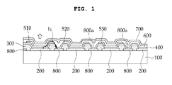
- FIG. 1 diagrammatically illustrates an example of an organic light emitting device according to the embodiments
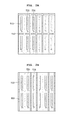
- FIGS. 2A to 2D diagrammatically illustrate planar dispositions of conductive material layers 800 in the organic light emitting device according to the embodiments;
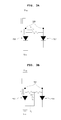
- FIG. 3A is a circuit diagram illustrating a flow of a leakage current in a conventional organic light emitting device
- FIG. 3B is a circuit diagram illustrating a flow of a leakage current in the organic light emitting device according to the embodiments, wherein a current is not leaked to an adjacent pixel;
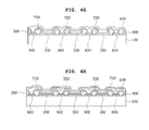
- FIGS. 4A to 4H diagrammatically illustrate an example of stages in a process of manufacturing an organic light emitting device according to the embodiments
- FIGS. 5A and 5B illustrate a state where leakage emission light is not generated by preventing a leakage current in the organic light emitting device according to the embodiments.
- the layer or element when it is described that a layer or element is located "on" another layer or element, the layer or element may not only directly contact the other layer or element, but also a third layer or element may be interposed therebetween.
- FIG. 1 diagrammatically illustrates an organic light emitting device according to the embodiments.
- the organic light emitting device is used in a display panel.
- the device is sometimes referred to as an organic light emitting display device.
- organic light emitting device is used herein.
- the organic light emitting device of FIG. 1 may include abase part 100, first electrodes 200 patterned on the base part 100, conductive material layers 800 spaced apart from the patterned first electrodes 200 and formed between the first electrodes 200, pixel defining layers 300 between the patterned first electrodes 200, light emitting layers 510, 520, and 530 formed on the first electrodes 200, and a second electrode 700 formed on the light emitting layers 510, 520, and 530.
- the organic light emitting device illustrated in FIG. 1 may include a first auxiliary light emitting layer 400 formed between the light emitting layers 510, 520, and 530 and the first electrodes 200 and a second auxiliary light emitting layer 600 formed between the light emitting layers 510, 520, and 530 and the second electrode 700.
- the light emitting layers 510, 520, and 530, the first auxiliary light emitting layer 400, and the second auxiliary light emitting layer 600 may correspond to organic layers.
- the conductive material layers 800 may be formed between the first electrodes 200, e.g., the first electrodes 200 and the conductive material layers 800 may alternate.
- the pixel defining layers 300 may be formed such that a portion of upper surfaces 800a of the conductive material layers 800 are exposed, i.e., not covered by the pixel defining layers 300.
- the pixel defining layers 300 may only partially overlap the conductive material layers 800.
- the pixel defining layers 300 may be formed between the first electrodes 200 and the conductive material layers 800, e.g., one pixel defining layer 300 may be between a first electrode 200 and an adjacent conductive material layer 800.
- the pixel defining layers (PDL) 300 may cover only a portion of an upper surface of the first electrodes 200 and the conductive material layers 800. A remaining portion of the upper surface of the first electrodes 200 and the conductive material layers 800 may be exposed, i.e., not covered by the pixel defining layers 300.
- the first electrodes 200 may be defined in units of pixels by the pixel defining layers 300.
- the pixel defining layers 300 adjacent each of the first electrodes 200 may define a pixel.
- the light emitting layers 510, 520, and 530 may be formed on the first electrodes 200, which may be defined in units of pixels by the pixel defining layers 300.
- the light emitting layers 510, 520, and 530 may include a red light emitting layer 510, a green light emitting layer 520, and a blue light emitting layer 530.
- the light emitting layers 510, 520, and 530 may include a red light emitting material, a green light emitting material, and a blue light emitting material, respectively.
- the light emitting materials may be organic materials. Any suitable light emitting materials known in the art may be used for the light emitting layers 510, 520, and 530.
- the first auxiliary light emitting layer 400 may be formed on an entire upper surface of the first electrodes 200, the conductive material layers 800, and the pixel defining layers 300.
- the first auxiliary light emitting layer 400 may be a hole injection layer and/or a hole transport layer.
- the first auxiliary light emitting layer 400 may include two layers, and may include both a hole injection layer and a hole transport layer separately. It is illustrated in the embodiment of FIG. 1 that the first auxiliary light emitting layer 400 is a hole injection and transport layer having both a hole injection function and a hole transport function.
- the second auxiliary light emitting layer 600 may be an electron injection layer and/or an electron transport layer.
- the second auxiliary light emitting layer 600 may include two layers, and may include both an electron injection layer and an electron transport layer separately. It is illustrated in the embodiment of FIG. 1 that the second auxiliary light emitting layer 600 is an electron transport layer.
- the first electrodes 200 may be anodes, functioning as pixel electrodes, and the second electrode 700 may be a cathode, functioning as a common electrode.
- the first electrodes 200, functioning as anodes, may be formed on the base part 100 in a patterned form.
- the first electrodes 200 may supply electric charges to the red light emitting layer 510, the green light emitting layer 520, and the blue light emitting layer 530.
- the red light emitting layer 510, the green light emitting layer 520, and the blue light emitting layer 530 formed on the first electrodes 200, may form a red pixel, a green pixel, and a blue pixel, respectively.
- the second electrode 700 i.e. the cathode, may be formed on an entire upper surface of the second auxiliary light emitting layer 600.
- FIGS. 2A to 2D illustrate exemplary planar dispositions of conductive material layers 800 in the organic light emitting device according to embodiments.
- the conductive material layers 800 may form a grid-like configuration between the patterned first electrodes 200.
- the conductive material layers 800 may surround the periphery of each of the first electrodes.
- the conductive material layers 800 may include line-shaped or linear portions which extend parallel to one another.
- the conductive material layers 800 may be comb-shaped, including a horizontal base portion, and vertical extensions that depend from the base portion between each of the patterned first electrodes 200.
- the conductive material layers 800 may be formed as fences, e.g., any suitable shape for surrounding a specific type, i.e., selected ones, of the light emitting layers.
- the conductive material layers 800 may surround the first electrodes 200 corresponding to the green light emitting layer 520.
- a green light emitting material has excellent efficiency. As such, leakage of emission light may be mainly generated in the green light emitting layer. Accordingly, the conductive material layers 800 may surround the first electrodes 200 corresponding to the green light emitting layer 520.
- the conductive material layers 800 may be formed between the first electrodes 200, and may be spaced apart from the first electrodes 200.
- each conductive material layer 800 may separate two adjacent first electrodes 200.
- the conductive material layers 800 may be electrically separated from the first electrodes 200.
- the pixel defining layers 300 may also be formed between the conductive material layers 800 and the first electrodes 200.
- the pixel defining layers 300 may be formed of an insulating material. Any suitable material known in the art may be used for the pixel defining layers 300.
- the pixel defining layer may also be referred to as a separation wall or a pixel definition line (PDL).
- PDL pixel definition line
- the pixel defining layers 300 may be formed between the first electrodes 200 to define the first electrodes 200 in units of pixels.
- the pixel defining layers 300 adjacent each of the first electrodes 200 may define a pixel.
- the pixel defining layers 300 may also be formed between the first electrodes 200 and the conductive material layers 800.
- the pixel defining layers 300 may not completely cover, i.e., may only partially overlap, the conductive material layers 800.
- the pixel defining layers 300 may cover only a portion of the upper surface 800a of the first electrodes 200 and the conductive material layers 800. A remaining portion of the upper surface of the first electrodes 200 and the conductive material layers 800 may be exposed, i.e., not covered by the pixel defining layers 300.
- the first auxiliary light emitting layer 400 may be disposed on the conductive material layer 800.
- the first auxiliary light emitting layer 400 may be formed on an entire upper surface of the first electrodes 200, the conductive material layers 800, and the pixel defining layers 300.
- the leakage currents IL generated in one light emitting layer 510 may not flow into an adjacent light emitting layer 520 but gather in the conductive material layers 800. Accordingly, the leakage currents IL may be prevented from flowing into the adjacent light emitting layer 520.
- the conductive material layers 800 may be electrically connected to a terminal having a voltage lower than that of the first electrodes 200. As an example, the conductive material layers 800 may be electrically connected to the cathode 700. The conductive material layers 800 may also be connected to a separate terminal, and may be connected to a ground terminal. As the conductive material layers 800 may be connected to the cathode or the ground terminal, the leakage currents IL having gathered in the conductive material layers 800 may be easily discharged.
- leakage emission light may be prevented from being generated in the light emitting layer 520 adjacent to the light emitting layer 510 where the leakage currents IL are generated.
- FIG. 3A illustrates a flow of a leakage current in a conventional organic light emitting device.
- FIG. 3B illustrates a flow of a leakage current in the organic light emitting device according to embodiments of the present invention.
- the leakage currents IL generated in the red light emitting layer 510 flow into the adjacent green light emitting layer 520. Even when the leakage currents IL constitute a small amount, they may cause the green light emitting layer 520 to emit light.
- the leakage currents IL generated in the red light emitting layer 510 flow through a path PL (leakage path) that is newly formed by the conductive material layer 800 instead of flowing into the green light emitting layer 520.
- path PL leakage path
- the leakage currents will flow to the cathode, and when the conductive material layer 800 is connected to a separate ground terminal, the leakage currents will flow to the ground line.
- leakage emission light is prevented from being generated in the light emitting layer 520 adjacent to the light emitting layer 510 where the leakage currents are generated.
- the conductive material layers 800 may be formed of a material that is the same as that of the first electrodes 200. According to some embodiments, the conductive material layers 800 may be formed of a material different from that of the first electrodes 200.
- the conductive material layers 800 may be a single layer or a plurality of stacked layers.
- the conductive material layers 800 may include at least one of a transparent conductive oxide (TCO) layer and a metal layer.
- TCO transparent conductive oxide
- the transparent conductive oxide (TCO) layer may include a suitable material generally used in the art.
- the transparent conductive oxide (TCO) layer may include at least one selected from an ITO (Indium Tin Oxide) layer, an IZO (Indium Zinc Oxide) layer, and an AZO (Aluminum-based Zinc Oxide) layer.
- the metal layer also may include a suitable material generally used in the art.
- the metal layer may include at least one material selected from a silver (Ag) layer, a copper (Cu) layer, and an aluminum (Al) layer.
- the conductive material layers 800 may be formed of a material other than the above-listed materials.
- the conductive material layers 800 may include, for example, a layer including ITO, which is widely used for a transparent electrode material, and a layer including silver (Ag), which has an excellent conductivity.
- the conductive material layers 800 may include, for example, a stacked structure in which an ITO layer, a silver (Ag) layer, and an ITO layer are sequentially stacked.
- the base part 100 may include a substrate, a TFT layer, and a flat insulation layer.
- the base part 100 may include only a substrate.
- the base part 100 may be a substrate.
- FIG. 1 does not illustrate all of the individual elements of the base part 100.
- FIGS. 4A to 4H diagrammatically illustrate stages in a process of manufacturing an organic light emitting device according to an embodiment.
- a base part 100 may be prepared first, and a material 201 for forming first electrodes and conductive material layers may be applied to the base part 100( FIG. 4A ).
- the process of preparing the base part 100 may include a step of preparing a substrate, a step of forming a TFT layer, and a step of forming a flat insulation layer.
- a description of the entire process to prepare the base part 100 will be omitted.
- only the substrate may be a base part.
- the method of applying a material 201 for forming the first electrodes and the conductive material layers may be any suitable method generally used in the art.
- An example of such a method may include sputtering.
- the first electrodes 200 and the conductive material layers 800 may be formed of a same material, as will be described with reference to FIGS. 4A to 4H . Accordingly, a material for forming both the first electrodes 200 and the conductive material layers 800 may be applied to the base part 100 in a whole, e.g., in one step.
- the first electrodes 200 and the conductive material layers 800 may include at least one of a transparent conductive oxide (TCO) layer and a metal layer. Accordingly, in the process of applying the material 201 for forming the first electrodes 200 and the conductive material layers 800, at least one of a step of forming a transparent conductive oxide (TCO) layer and a step of forming a metal layer may be included.
- the transparent conductive oxide (TCO) layer may include at least one of an ITO layer, an IZO layer, and an AZO layer.
- the metal layer may include at least one of a silver (Ag) layer, a copper (Cu) layer, and an aluminum layer (Al).
- the first electrodes 200 and the conductive material layers 800 may include an ITO layer, a silver (Ag) layer, and an ITO layer stacked, in that order.
- a step of forming an ITO layer, a step of forming a silver (Ag) layer, and a step of forming an ITO layer may be sequentially performed.
- the first electrodes 200 and the conductive material layers 800 may be formed by patterning the material 201 for forming the first electrodes and the conductive material layers, which are applied on the base part 100 ( FIG. 4B ). Any suitable method patterning method generally known in the art may be used.
- the first electrodes 200 and the conductive material layers 800 may be patterned simultaneously.
- the conductive material layers 800 may be formed between the patterns of the first electrodes 200 and may be spaced apart from the patterns of the first electrodes 200.
- the conductive material layers 800 when the conductive material layers 800 are patterned, the conductive material layers 800 may be formed between the first electrodes 200 in any one of a grid, line, or comb-shape, as described above. According to some other embodiments, when the conductive material layers 800 are patterned, the conductive material layers 800 may surround only the first electrodes 200 corresponding to the green light emitting layer.
- a pixel defining layer forming material 301 may be applied on the patterned first electrodes 200 and conductive material layers 800 ( FIG. 4C ).
- the pixel defining layer forming material 301 may be an electrically insulating material.
- the pixel defining layer forming material 301 may be formed from any suitable material generally known in the art.
- the pixel defining layers 300 may be formed by patterning the pixel defining layer forming material 301 ( FIG. 4D ). Any suitable patterning method generally known in the art may be used.
- the pixel defining layers 300 may be formed between the first electrodes 200 such that upper portions of the conductive material layers 800 may be exposed. For example, the pixel defining layers 300 may only partially overlap the conductive material layers 800.
- the pixel defining layers 300 may be formed between the first electrodes 200 and the conductive material layers 800. Upper portions of the first electrodes 200 and upper portions of the conductive material layers 800 may be partially exposed. For example, the pixel defining layers 300 may only partially overlap the conductive material layers 800 and the first electrodes 200. The pixel defining layers 300 may be formed only between the first electrodes 200 when there is no conductive material layer 800 between the first electrodes 200. For example, each of the pixel defining layers 300 may contact two adjacent first electrodes 200 when a conductive material layer 800 is not disposed between the two adjacent first electrodes 200.
- a first auxiliary light emitting layer 400 may be formed before the light emitting layers 510, 520, and 530 are formed ( FIG. 4E ). As can be seen in FIG. 4E , the first auxiliary light emitting layer 400 may be formed on a surface, e.g., an entire surface, of the first electrodes 200, the conductive material layers 800, and the pixel defining layers 300.
- the first auxiliary light emitting layer 400 may be any one of a hole injection layer and a hole transport layer and may include both a hole injection layer and a hole transport layer.
- FIG. 4E illustrates a hole injection and a hole transport layer, having both a hole injection function and a hole transport function, as the auxiliary light emitting layer 400.
- the step of forming the first auxiliary light emitting layer 400 may include at least one of a step of forming a hole injection layer and a hole transport layer, and may also include both steps.
- the first auxiliary light emitting layer 400 may include two layers, the hole injection layer and the hole transport layer.
- the hole injection layer may be formed before the hole transport layer is formed.
- light emitting layers 510, 520, and 530 may be formed on the first auxiliary light emitting layer 400 ( FIG. 4F ).
- the light emitting layers 510, 520, and 530 may be disposed on the first electrodes 200 defined in units of pixels by the pixel defining layers 300.
- the light emitting layers may include the red light emitting layer 510, the green light emitting layer 520, and the blue light emitting layer 530. Any suitable method of preparing light emitting layers generally known in the art may be used to prepare the light emitting layers 510, 520, and 530. Therefore, a specific description of preparing the light emitting layers is omitted.
- a second auxiliary light emitting layer 600 may be formed after the light emitting layers 510, 520, and 530 are formed and before the second electrode 700 is formed ( FIG. 4G ).
- the second auxiliary light emitting layer 600 may include at least one of an electron injection layer and an electron transport layer. Accordingly, the step of forming the second auxiliary light emitting layer 600 may include at least one of a step of forming a hole injection layer and a step of forming a hole transport layer. According to an embodiment, the second auxiliary light emitting layer 600 may be an electron transport layer. Accordingly, FIG. 4G illustrates that an electron transport layer is formed as the second auxiliary light emitting layer 600. However, the second auxiliary light emitting layer 600 may include two layers, and may include both an electron injection layer and an electron transport layer separately.
- a second electrode 700 may be formed on the second auxiliary light emitting layer 600 ( FIG. 4H ).
- the organic light emitting device according to the embodiments may be manufactured through the above-described process.
- FIGS. 5A and 5B show emission of light of the organic light emitting device manufactured according to one or more embodiments of the present invention.
- FIG. 5A when red pixels R are turned on, only the red pixels R emit light.
- FIG. 5B when blue pixels B are turned on, only the blue pixels B emit light.
- the organic light emitting device according to the embodiments may prevent generation of leakage currents without causing leakage emission light.
- the organic light emitting device may prevent a leakage current that flows from one pixel to an adjacent pixel of a light emitting part (which is generated when driving a pixel). Accordingly, an undesired emission of light in the adjacent pixel may be prevented. As a result, colors can be accurately realized, and light emitting quality can be improved. Leakage emission light due to a leakage current can be restrained, even in an organic light emitting device of a high resolution which uses a light emitting material of a high efficiency. Accordingly, the organic light emitting device according to the embodiments, can improve color realization and light emitting quality while satisfying a recent increased demand for products of low power consumption and high resolution.
Landscapes
- Engineering & Computer Science (AREA)
- Physics & Mathematics (AREA)
- Optics & Photonics (AREA)
- Microelectronics & Electronic Packaging (AREA)
- Manufacturing & Machinery (AREA)
- Electroluminescent Light Sources (AREA)
Description
- The embodiments relate to an organic light emitting device having improved light emitting quality by reducing leakage current between pixels.
- In recent years, organic light emitting devices are being spotlighted in the field of display technology. The organic light emitting devices emitting light, which is generated when electrons and holes recombine and then decay.
- The organic light emitting device basically includes an electrode for injecting holes, an electrode for injecting electrons, and a light emitting layer. The organic light emitting device has a structure in which the light emitting layer is stacked between an anode, i.e. the electrode for injecting the holes, and a cathode, i.e. the electrode for injecting the electrons. In more detail, electrons are injected in a cathode of the organic light emitting device and holes are injected in an anode of the organic light emitting device. When the charges (holes and electrons) are moved in opposite directions by an external electric field, holes and electrons recombine forming an exciton, which then decays and thus emits light. The light emitting layer of the organic light emitting device includes an organic monomer or an organic polymer.
- In recent years, as resolutions of displays are getting higher, resolutions of the pixels (ppi) have increased, and the interval between the pixels have gradually decreased. Further, in recent years, as efficiencies of light emitting materials for organic light emitting devices are increasing, a high brightness can be achieved with a low current and a low voltage, making it possible to lower power consumption. However, as light can be emitted by a small amount of current (due to a high efficiency of a light emitting material for an organic light emitting device) light may be emitted by a very small amount of current leaked from one pixel to another adjacent pixel. As a result, an adjacent pixel, which is not intended to emit light, often emits light.
- The light emitted due to leakage currents is referred to as leakage emission light. If the leakage emission light is generated, a color mixture is generated and a color coordinate is changed. In addition, when the leakage emission due to a leakage current is generated in a low-brightness region, black brightness may increase.
- In particular, a green light emitting material has a high efficiency. Thus, when a red pixel or a blue pixel adjacent to a green pixel is driven, the adjacent green pixel may emit light due to current leakage from the red or blue driven pixel.
- The leakage emission light is one of the phenomena generated as an efficiency of a light emitting material and a resolution of a display increase. Accordingly, a method of lowering an efficiency of a light emitting material or lowering a resolution of a display device may be adopted to restrain a leakage emission light. However, a demand for low-power/high-resolution products has also increased in recent years. As such, the problem of leakage emission light must be resolved without lowering the efficiency of a light emitting material or lowering the resolution of a display device.
- Therefore, a technology for restraining a leakage emission light due to leakage currents, without lowering a resolution of a display unit using a high-efficiency light emitting material is needed.
- One or more embodiments may provide an organic light emitting device, including a base part, patterned first electrodes on the base part, conductive material layers spaced apart from the patterned first electrodes and between the first electrodes, pixel defining layers between the patterned first electrodes, the pixel defining layers overlapping only a portion of upper surfaces of the conductive material layers; light emitting layers on the first electrodes, and a second electrode on the light emitting layers.
- The organic light emitting device may further include at least one first auxiliary light emitting layer between the light emitting layers and the first electrodes. The first auxiliary light emitting layer may include at least one of a hole injection layer and a hole transport layer.
- The organic light emitting device may further include a second auxiliary light emitting layer between the light emitting layers and the second electrode. The second auxiliary light emitting layer may include at least one of an electron injection layer and an electron transport layer.
- The first electrodes may be pixel electrodes. The first electrodes may be anodes and the second electrode may be a cathode. A material included in the conductive material layers and the first electrodes may be the same. The conductive material layers may include at least one of a transparent conductive oxide (TCO) layer and a metal layer. The transparent conductive oxide (TCO) layer may include at least one of an ITO layer, an IZO layer, and an AZO layer. The metal layer may include at least one of a silver (Ag) layer, a copper (Cu) layer, and an aluminum (Al) layer. The conductive material layers may include an ITO layer, a silver (Ag) layer, and an ITO layer, stacked in that order. The conductive material layers may be electrically connected to a terminal having a voltage lower than that of the first electrodes. The conductive material layers may be electrically connected to a cathode. The conductive material layers may be between the first electrodes and have a mesh-shape, a line-shape, or a comb-shape.
- The light emitting layers may include a red light emitting layer, a green light emitting layer, and a blue light emitting layer, and the conductive material layers may surround the first electrodes corresponding to the green light emitting layer. The base part may include a substrate, a TFT layer, and a flat insulating layer. Alternatively, the base part may be a substrate.
- One or more embodiments may provide a method of manufacturing an organic light emitting device, including forming patterns of first electrodes on a base part, forming conductive material layers between the patterned first electrodes, the conductive material layers being spaced apart from the first electrodes, forming pixel defining layers (PDLs) between the patterned first electrodes, the pixel defining layers overlapping only a portion of upper surfaces of the conductive material layers, forming light emitting layers on the first electrodes; and forming a second electrode on the light emitting layers.
- The method may further include forming at least one first auxiliary light emitting layer after forming the pixel defining layers and before forming the light emitting layers. Forming the first auxiliary light emitting layer may include forming at least one of a hole injection layer and forming a hole transport layer. The method may further include forming at least one second auxiliary light emitting layer after forming the light emitting layers and before forming the second electrode. The second auxiliary light emitting layer may include forming at least one of an electron transport layer and an electron injection layer. Forming the conductive material layers and forming the patterns of the first electrodes may be performed simultaneously. Forming the conductive material layers may include forming at least one of a transparent conductive oxide (TCO) layer and a metal layer. The transparent conductive oxide (TCO) layer may include at least one of an ITO layer, an IZO layer, and an AZO layer. The metal layer may include at least one of a silver (Ag) layer, a copper (Cu) layer, and an aluminum (A1) layer. Forming the conductive material layers may include forming an ITO layer, forming a silver (Ag) layer, and forming an ITO layer, in that order. The conductive material layers may be formed in any one of a mesh-shape, a line-shape, and a comb-shape.
- Forming the light emitting layers may include forming a red light emitting layer, forming a green light emitting layer, and forming a blue light emitting layer, the conductive material layers being formed to surrounding the first electrodes corresponding to the green light emitting layer. The first electrodes may be anodes and the second electrode may be a cathode, and forming the second electrode may include electrically connecting the conductive material layers to the second electrode. The method may further include electrically connecting the conductive material layers to the ground terminal during or after forming the conductive material layers, wherein the organic light emitting device includes a ground terminal, and the ground terminal has a voltage lower than that of the first electrodes.
- An organic light emitting device may include a base part, first electrode patterns on the base part, conductive material layers spaced apart from the first electrode patterns and disposed between the first electrode patterns, pixel defining layers between the first electrode patterns, the pixel defining layers overlapping only a portion of upper surfaces of the conductive material layers, at least one first auxiliary light emitting layer on the first electrode patterns, the conductive material layers, and the pixel defining layers, light emitting layers on the first auxiliary light emitting layer, at least one second auxiliary light emitting layer on the light emitting layers, and a second electrode on the second auxiliary light emitting layer, wherein the light emitting layers are formed on the first electrode patterns. The first auxiliary light emitting layer may include at least one of a hole injection layer and a hole transport layer. The second auxiliary light emitting layer may include at least one of an electron injection layer and an electron transport layer.
- One or more embodiments may provide a method of manufacturing an organic light emitting device, including forming first electrode patterns on a base part, forming conductive material layers between the first electrode patterns, the conductive material layers being spaced apart from the first electrode patterns, forming pixel defining layers between the first electrode patterns, the pixel defining layers overlapping only a portion of upper surfaces of the conductive material layers; forming at least one first auxiliary light emitting layer on the first electrode patterns, the conductive material layers, and the pixel defining layers, forming light emitting layers on the first auxiliary light emitting layer, forming at least one second auxiliary light emitting layer on the light emitting layers, and forming a second electrode on the second auxiliary light emitting layer, wherein the light emitting layers are formed on the first electrode patterns. Forming the first auxiliary light emitting layer may include at least one of forming a hole injection layer; and forming a hole transport layer. Forming the second auxiliary light emitting layer may include at least one of forming an electron injection layer, and forming an electron transport layer.
- The first electrodes may be anodes and the second electrode may be a cathode, and forming the second electrode includes electrically connecting the conductive material layers to the second electrode. The method may further include electrically connecting the conductive material layers to the ground terminal during or after forming the conductive material layers, wherein the organic light emitting device includes a ground terminal, and the ground terminal has a voltage lower than that of the first electrodes.
- The above and other objects, features and advantages of the embodiments will be more apparent from the following detailed description taken in conjunction with the accompanying drawings, in which:
-
FIG. 1 diagrammatically illustrates an example of an organic light emitting device according to the embodiments; -
FIGS. 2A to 2D diagrammatically illustrate planar dispositions of conductive material layers 800 in the organic light emitting device according to the embodiments; -
FIG. 3A is a circuit diagram illustrating a flow of a leakage current in a conventional organic light emitting device; -
FIG. 3B is a circuit diagram illustrating a flow of a leakage current in the organic light emitting device according to the embodiments, wherein a current is not leaked to an adjacent pixel; -
FIGS. 4A to 4H diagrammatically illustrate an example of stages in a process of manufacturing an organic light emitting device according to the embodiments; -
FIGS. 5A and 5B illustrate a state where leakage emission light is not generated by preventing a leakage current in the organic light emitting device according to the embodiments. - Hereinafter, an exemplary embodiment will be described in more detail with reference to the accompanying drawings. However, the scope of the embodiments is not limited to the below-described embodiments and the drawings.
- For reference, the elements and their shapes may be drawn or exaggerated in the drawings to facilitate an understanding of the embodiments. In the drawings, the same reference numerals denote the same elements.
- Further, when it is described that a layer or element is located "on" another layer or element, the layer or element may not only directly contact the other layer or element, but also a third layer or element may be interposed therebetween.
-
FIG. 1 diagrammatically illustrates an organic light emitting device according to the embodiments. The organic light emitting device is used in a display panel. Thus, the device is sometimes referred to as an organic light emitting display device. However, the term "organic light emitting device" is used herein. - The organic light emitting device of
FIG. 1 may includeabase part 100,first electrodes 200 patterned on thebase part 100, conductive material layers 800 spaced apart from the patternedfirst electrodes 200 and formed between thefirst electrodes 200,pixel defining layers 300 between the patternedfirst electrodes 200, light emittinglayers first electrodes 200, and asecond electrode 700 formed on thelight emitting layers FIG. 1 may include a first auxiliarylight emitting layer 400 formed between the light emittinglayers first electrodes 200 and a second auxiliarylight emitting layer 600 formed between the light emittinglayers second electrode 700. - The
light emitting layers light emitting layer 400, and the second auxiliarylight emitting layer 600 may correspond to organic layers. - Referring to
FIG. 1 , the conductive material layers 800 may be formed between thefirst electrodes 200, e.g., thefirst electrodes 200 and the conductive material layers 800 may alternate. Thepixel defining layers 300 may be formed such that a portion ofupper surfaces 800a of the conductive material layers 800 are exposed, i.e., not covered by thepixel defining layers 300. For example, thepixel defining layers 300 may only partially overlap the conductive material layers 800. Thepixel defining layers 300 may be formed between thefirst electrodes 200 and the conductive material layers 800, e.g., onepixel defining layer 300 may be between afirst electrode 200 and an adjacentconductive material layer 800. The pixel defining layers (PDL) 300 may cover only a portion of an upper surface of thefirst electrodes 200 and the conductive material layers 800. A remaining portion of the upper surface of thefirst electrodes 200 and the conductive material layers 800 may be exposed, i.e., not covered by thepixel defining layers 300. - The
first electrodes 200 may be defined in units of pixels by thepixel defining layers 300. For example, thepixel defining layers 300 adjacent each of thefirst electrodes 200 may define a pixel. Thelight emitting layers first electrodes 200, which may be defined in units of pixels by thepixel defining layers 300. - The
light emitting layers light emitting layer 510, a greenlight emitting layer 520, and a bluelight emitting layer 530. Thelight emitting layers light emitting layers - It can be seen from
FIG. 1 that the first auxiliarylight emitting layer 400 may be formed on an entire upper surface of thefirst electrodes 200, the conductive material layers 800, and thepixel defining layers 300. The first auxiliarylight emitting layer 400 may be a hole injection layer and/or a hole transport layer. The first auxiliarylight emitting layer 400 may include two layers, and may include both a hole injection layer and a hole transport layer separately. It is illustrated in the embodiment ofFIG. 1 that the first auxiliarylight emitting layer 400 is a hole injection and transport layer having both a hole injection function and a hole transport function. - The second auxiliary
light emitting layer 600 may be an electron injection layer and/or an electron transport layer. The second auxiliarylight emitting layer 600 may include two layers, and may include both an electron injection layer and an electron transport layer separately. It is illustrated in the embodiment ofFIG. 1 that the second auxiliarylight emitting layer 600 is an electron transport layer. - In the embodiment of
FIG. 1 , thefirst electrodes 200 may be anodes, functioning as pixel electrodes, and thesecond electrode 700 may be a cathode, functioning as a common electrode. Thefirst electrodes 200, functioning as anodes, may be formed on thebase part 100 in a patterned form. - The
first electrodes 200 may supply electric charges to the redlight emitting layer 510, the greenlight emitting layer 520, and the bluelight emitting layer 530. The redlight emitting layer 510, the greenlight emitting layer 520, and the bluelight emitting layer 530 formed on thefirst electrodes 200, may form a red pixel, a green pixel, and a blue pixel, respectively. - The
second electrode 700, i.e. the cathode, may be formed on an entire upper surface of the second auxiliarylight emitting layer 600. -
FIGS. 2A to 2D illustrate exemplary planar dispositions of conductive material layers 800 in the organic light emitting device according to embodiments. - According to some embodiments, as illustrated in
FIG. 2A , the conductive material layers 800 may form a grid-like configuration between the patternedfirst electrodes 200. For example, the conductive material layers 800 may surround the periphery of each of the first electrodes. According to some embodiments, as illustrated inFIG. 2B , the conductive material layers 800 may include line-shaped or linear portions which extend parallel to one another. According to some embodiments, as illustrated inFIG. 2C , the conductive material layers 800 may be comb-shaped, including a horizontal base portion, and vertical extensions that depend from the base portion between each of the patternedfirst electrodes 200. - As illustrated in
FIG. 2D , the conductive material layers 800 may be formed as fences, e.g., any suitable shape for surrounding a specific type, i.e., selected ones, of the light emitting layers. For example, the conductive material layers 800 may surround thefirst electrodes 200 corresponding to the greenlight emitting layer 520. A green light emitting material has excellent efficiency. As such, leakage of emission light may be mainly generated in the green light emitting layer. Accordingly, the conductive material layers 800 may surround thefirst electrodes 200 corresponding to the greenlight emitting layer 520. - As illustrated in
FIG. 1 , the conductive material layers 800 may be formed between thefirst electrodes 200, and may be spaced apart from thefirst electrodes 200. For example, eachconductive material layer 800 may separate two adjacentfirst electrodes 200. The conductive material layers 800 may be electrically separated from thefirst electrodes 200. Accordingly, thepixel defining layers 300 may also be formed between the conductive material layers 800 and thefirst electrodes 200. Thepixel defining layers 300 may be formed of an insulating material. Any suitable material known in the art may be used for thepixel defining layers 300. The pixel defining layer may also be referred to as a separation wall or a pixel definition line (PDL). The phrase "pixel defining layer" is used herein. - The
pixel defining layers 300 may be formed between thefirst electrodes 200 to define thefirst electrodes 200 in units of pixels. For example, thepixel defining layers 300 adjacent each of thefirst electrodes 200 may define a pixel. Thepixel defining layers 300 may also be formed between thefirst electrodes 200 and the conductive material layers 800. Thepixel defining layers 300 may not completely cover, i.e., may only partially overlap, the conductive material layers 800. For example, thepixel defining layers 300 may cover only a portion of theupper surface 800a of thefirst electrodes 200 and the conductive material layers 800. A remaining portion of the upper surface of thefirst electrodes 200 and the conductive material layers 800 may be exposed, i.e., not covered by thepixel defining layers 300. - The first auxiliary
light emitting layer 400 may be disposed on theconductive material layer 800. The first auxiliarylight emitting layer 400 may be formed on an entire upper surface of thefirst electrodes 200, the conductive material layers 800, and thepixel defining layers 300. - As the conductive material layers 800 may be formed in the above-described way, the leakage currents IL generated in one
light emitting layer 510 may not flow into an adjacentlight emitting layer 520 but gather in the conductive material layers 800. Accordingly, the leakage currents IL may be prevented from flowing into the adjacentlight emitting layer 520. - The conductive material layers 800 may be electrically connected to a terminal having a voltage lower than that of the
first electrodes 200. As an example, the conductive material layers 800 may be electrically connected to thecathode 700. The conductive material layers 800 may also be connected to a separate terminal, and may be connected to a ground terminal. As the conductive material layers 800 may be connected to the cathode or the ground terminal, the leakage currents IL having gathered in the conductive material layers 800 may be easily discharged. - As a result, leakage emission light may be prevented from being generated in the
light emitting layer 520 adjacent to thelight emitting layer 510 where the leakage currents IL are generated. - In this regard,
FIG. 3A illustrates a flow of a leakage current in a conventional organic light emitting device.FIG. 3B illustrates a flow of a leakage current in the organic light emitting device according to embodiments of the present invention. - It can be seen from
FIG. 3A that the leakage currents IL generated in the redlight emitting layer 510 flow into the adjacent greenlight emitting layer 520. Even when the leakage currents IL constitute a small amount, they may cause the greenlight emitting layer 520 to emit light. - According to an embodiment of the present invention shown in
FIG. 3B the leakage currents IL generated in the redlight emitting layer 510 flow through a path PL (leakage path) that is newly formed by theconductive material layer 800 instead of flowing into the greenlight emitting layer 520. When theconductive material layer 800 is electrically connected to the cathode, the leakage currents will flow to the cathode, and when theconductive material layer 800 is connected to a separate ground terminal, the leakage currents will flow to the ground line. As a result, leakage emission light is prevented from being generated in thelight emitting layer 520 adjacent to thelight emitting layer 510 where the leakage currents are generated. - According to some embodiments, the conductive material layers 800 may be formed of a material that is the same as that of the
first electrodes 200. According to some embodiments, the conductive material layers 800 may be formed of a material different from that of thefirst electrodes 200. - The conductive material layers 800 may be a single layer or a plurality of stacked layers. The conductive material layers 800 may include at least one of a transparent conductive oxide (TCO) layer and a metal layer.
- The transparent conductive oxide (TCO) layer may include a suitable material generally used in the art. For example, the transparent conductive oxide (TCO) layer may include at least one selected from an ITO (Indium Tin Oxide) layer, an IZO (Indium Zinc Oxide) layer, and an AZO (Aluminum-based Zinc Oxide) layer.
- The metal layer also may include a suitable material generally used in the art. For example, the metal layer may include at least one material selected from a silver (Ag) layer, a copper (Cu) layer, and an aluminum (Al) layer.
- It is apparent that the conductive material layers 800 may be formed of a material other than the above-listed materials.
- The conductive material layers 800 may include, for example, a layer including ITO, which is widely used for a transparent electrode material, and a layer including silver (Ag), which has an excellent conductivity. The conductive material layers 800 may include, for example, a stacked structure in which an ITO layer, a silver (Ag) layer, and an ITO layer are sequentially stacked.
- According to some embodiments, the
base part 100 may include a substrate, a TFT layer, and a flat insulation layer. Thebase part 100 may include only a substrate. According to some embodiments, thebase part 100 may be a substrate. - For simplicity,
FIG. 1 does not illustrate all of the individual elements of thebase part 100. -
FIGS. 4A to 4H diagrammatically illustrate stages in a process of manufacturing an organic light emitting device according to an embodiment. - A
base part 100 may be prepared first, and amaterial 201 for forming first electrodes and conductive material layers may be applied to the base part 100(FIG. 4A ). - According to some embodiments, the process of preparing the
base part 100 may include a step of preparing a substrate, a step of forming a TFT layer, and a step of forming a flat insulation layer. In the present embodiment, a description of the entire process to prepare thebase part 100 will be omitted. Further, according to the present embodiment, only the substrate may be a base part. - The method of applying a
material 201 for forming the first electrodes and the conductive material layers may be any suitable method generally used in the art. An example of such a method may include sputtering. - According to some embodiments, the
first electrodes 200 and the conductive material layers 800 may be formed of a same material, as will be described with reference toFIGS. 4A to 4H . Accordingly, a material for forming both thefirst electrodes 200 and the conductive material layers 800 may be applied to thebase part 100 in a whole, e.g., in one step. - The
first electrodes 200 and the conductive material layers 800 may include at least one of a transparent conductive oxide (TCO) layer and a metal layer. Accordingly, in the process of applying thematerial 201 for forming thefirst electrodes 200 and the conductive material layers 800, at least one of a step of forming a transparent conductive oxide (TCO) layer and a step of forming a metal layer may be included. Here, the transparent conductive oxide (TCO) layer may include at least one of an ITO layer, an IZO layer, and an AZO layer. The metal layer may include at least one of a silver (Ag) layer, a copper (Cu) layer, and an aluminum layer (Al). - Meanwhile, the
first electrodes 200 and the conductive material layers 800 may include an ITO layer, a silver (Ag) layer, and an ITO layer stacked, in that order. In order to form thefirst electrodes 200 and the conductive material layers 800, a step of forming an ITO layer, a step of forming a silver (Ag) layer, and a step of forming an ITO layer may be sequentially performed. - The
first electrodes 200 and the conductive material layers 800 may be formed by patterning thematerial 201 for forming the first electrodes and the conductive material layers, which are applied on the base part 100 (FIG. 4B ). Any suitable method patterning method generally known in the art may be used. - The
first electrodes 200 and the conductive material layers 800 may be patterned simultaneously. The conductive material layers 800 may be formed between the patterns of thefirst electrodes 200 and may be spaced apart from the patterns of thefirst electrodes 200. - According to some embodiments, when the conductive material layers 800 are patterned, the conductive material layers 800 may be formed between the
first electrodes 200 in any one of a grid, line, or comb-shape, as described above. According to some other embodiments, when the conductive material layers 800 are patterned, the conductive material layers 800 may surround only thefirst electrodes 200 corresponding to the green light emitting layer. - A pixel defining
layer forming material 301 may be applied on the patternedfirst electrodes 200 and conductive material layers 800 (FIG. 4C ). The pixel defininglayer forming material 301 may be an electrically insulating material. The pixel defininglayer forming material 301 may be formed from any suitable material generally known in the art. - The
pixel defining layers 300 may be formed by patterning the pixel defining layer forming material 301 (FIG. 4D ). Any suitable patterning method generally known in the art may be used. Thepixel defining layers 300 may be formed between thefirst electrodes 200 such that upper portions of the conductive material layers 800 may be exposed. For example, thepixel defining layers 300 may only partially overlap the conductive material layers 800. - As shown in
FIG. 4D , thepixel defining layers 300 may be formed between thefirst electrodes 200 and the conductive material layers 800. Upper portions of thefirst electrodes 200 and upper portions of the conductive material layers 800 may be partially exposed. For example, thepixel defining layers 300 may only partially overlap the conductive material layers 800 and thefirst electrodes 200. Thepixel defining layers 300 may be formed only between thefirst electrodes 200 when there is noconductive material layer 800 between thefirst electrodes 200. For example, each of thepixel defining layers 300 may contact two adjacentfirst electrodes 200 when aconductive material layer 800 is not disposed between the two adjacentfirst electrodes 200. - A first auxiliary
light emitting layer 400 may be formed before thelight emitting layers FIG. 4E ). As can be seen inFIG. 4E , the first auxiliarylight emitting layer 400 may be formed on a surface, e.g., an entire surface, of thefirst electrodes 200, the conductive material layers 800, and thepixel defining layers 300. The first auxiliarylight emitting layer 400 may be any one of a hole injection layer and a hole transport layer and may include both a hole injection layer and a hole transport layer. -
FIG. 4E illustrates a hole injection and a hole transport layer, having both a hole injection function and a hole transport function, as the auxiliarylight emitting layer 400. The step of forming the first auxiliarylight emitting layer 400 may include at least one of a step of forming a hole injection layer and a hole transport layer, and may also include both steps. For example, the first auxiliarylight emitting layer 400 may include two layers, the hole injection layer and the hole transport layer. The hole injection layer may be formed before the hole transport layer is formed. Thereafter, light emittinglayers FIG. 4F ). - The
light emitting layers first electrodes 200 defined in units of pixels by thepixel defining layers 300. The light emitting layers may include the redlight emitting layer 510, the greenlight emitting layer 520, and the bluelight emitting layer 530. Any suitable method of preparing light emitting layers generally known in the art may be used to prepare thelight emitting layers - According to the present embodiment, a second auxiliary
light emitting layer 600 may be formed after thelight emitting layers second electrode 700 is formed (FIG. 4G ). - The second auxiliary
light emitting layer 600 may include at least one of an electron injection layer and an electron transport layer. Accordingly, the step of forming the second auxiliarylight emitting layer 600 may include at least one of a step of forming a hole injection layer and a step of forming a hole transport layer. According to an embodiment, the second auxiliarylight emitting layer 600 may be an electron transport layer. Accordingly,FIG. 4G illustrates that an electron transport layer is formed as the second auxiliarylight emitting layer 600. However, the second auxiliarylight emitting layer 600 may include two layers, and may include both an electron injection layer and an electron transport layer separately. - Next, a
second electrode 700 may be formed on the second auxiliary light emitting layer 600 (FIG. 4H ). The organic light emitting device according to the embodiments may be manufactured through the above-described process. -
FIGS. 5A and 5B show emission of light of the organic light emitting device manufactured according to one or more embodiments of the present invention. As shown inFIG. 5A , when red pixels R are turned on, only the red pixels R emit light. As shown inFIG. 5B , when blue pixels B are turned on, only the blue pixels B emit light. In this way, the organic light emitting device according to the embodiments may prevent generation of leakage currents without causing leakage emission light. - The organic light emitting device, according to the embodiments, may prevent a leakage current that flows from one pixel to an adjacent pixel of a light emitting part (which is generated when driving a pixel). Accordingly, an undesired emission of light in the adjacent pixel may be prevented. As a result, colors can be accurately realized, and light emitting quality can be improved. Leakage emission light due to a leakage current can be restrained, even in an organic light emitting device of a high resolution which uses a light emitting material of a high efficiency. Accordingly, the organic light emitting device according to the embodiments, can improve color realization and light emitting quality while satisfying a recent increased demand for products of low power consumption and high resolution.
Claims (17)
- An organic light emitting device, comprising:a base part (100);patterned first electrodes (200) on the base part (100);conductive material layers (800) between the first electrodes (200) and spaced apart from the patterned first electrodes (200);pixel defining layers (300) between the patterned first electrodes (200), the pixel defining layers (300) overlapping only a portion of upper surfaces of the conductive material layers (800);light emitting layers (510, 520, 530) on the first electrodes (200); anda second electrode (700) on the light emitting layers (510, 520, 530).
- The organic light emitting device as claimed in claim 1, further comprising one first auxiliary light emitting layer (400) between the light emitting layers (510, 520, 530) and the first electrodes (200) and/or a second auxiliary light emitting layer (600) between the light emitting layers(510, 520, 530) and the second electrode (700).
- The organic light emitting device as claimed in one of the preceding claims, wherein the first electrodes (200) are anodes and the second electrode (700) is a cathode.
- The organic light emitting device as claimed in one of the preceding claims, wherein a material included in the conductive material layers (800) and the first electrodes (200) is the same.
- The organic light emitting device as claimed in one of the preceding claims, wherein the conductive material layers (800) include at least one of a transparent conductive oxide (TCO) layer and a metal layer.
- The organic light emitting device as claimed in claim 5, wherein the transparent conductive oxide (TCO) layer includes at least one of an ITO layer, an IZO layer, and an AZO layer.
- The organic light emitting device as claimed in one of claims 5 and 6, wherein the metal layer includes at least one of a silver (Ag) layer, a copper (Cu) layer, and an aluminum (Al) layer.
- The organic light emitting device as claimed in one of the preceding claims, wherein the conductive material layers (800) include an ITO layer, a silver (Ag) layer, and an ITO layer, stacked in that order.
- The organic light emitting device as claimed in one of the preceding claims, wherein the conductive material layers (800) are electrically connected to a terminal having a voltage lower than that of the first electrodes (200) or to a cathode.
- The organic light emitting device as claimed in one of the preceding claims, wherein the conductive material layers (800) are located between the first electrodes (200) and have a grid-shape, a line-shape, or a comb-shape.
- The organic light emitting device as claimed in one of claims 1 to 9,
wherein the light emitting layers (510, 520, 530) include a red light emitting layer (510), a green light emitting layer (520), and a blue light emitting layer (530), and the conductive material layers (800) surround the first electrodes (200) corresponding to the green light emitting layer (520). - A method of manufacturing an organic light emitting device according to one of the preceding claims, the method including:forming patterns of first electrodes (200) on a base part (100);forming conductive material layers (800) between the patterned first electrodes (200), the conductive material layers (800) being spaced apart from the first electrodes (200);forming pixel defining layers (300) between the patterned first electrodes (200), the pixel defining layers (300) overlapping only a portion of upper surfaces of the conductive material layers (800);forming light emitting layers (510, 520, 530) on the first electrodes (200); andforming a second electrode (700) on the light emitting layers (510, 520, 530).
- The method as claimed in claim 12, further comprising forming at least one first auxiliary light emitting layer (400) after forming the pixel defining layers (300) and before forming the light emitting layers (510, 520, 530).
- The method as claimed in one of claims 12 and 13, further comprising forming at least one second auxiliary light emitting layer (600) after forming the light emitting layers (510, 520, 530) and before forming the second electrode (700).
- The method as claimed in one of claims 12 to 14, wherein the conductive material layers (800) and the patterns of the first electrodes (200) are formed in a single step.
- The method as claimed in one of claims 12 to 15, wherein
the first electrodes (200) are anodes and the second electrode (700) is a cathode,
and
forming the second electrode (700) includes electrically connecting the conductive material layers (800) to the second electrode (700). - The method as claimed in one of claims 12 to 15, further comprising:electrically connecting the conductive material layers (800) to the ground terminal during or after forming the conductive material layers (800),
wherein the organic light emitting device includes a ground terminal, and the ground terminal has a voltage lower than that of the first electrodes (200).
Applications Claiming Priority (1)
| Application Number | Priority Date | Filing Date | Title |
|---|---|---|---|
| KR1020110127826A KR101647160B1 (en) | 2011-12-01 | 2011-12-01 | Organic light emitting device having improved light emitting quality by reducing leakage current between pixels |
Publications (3)
| Publication Number | Publication Date |
|---|---|
| EP2600401A2 true EP2600401A2 (en) | 2013-06-05 |
| EP2600401A3 EP2600401A3 (en) | 2015-08-26 |
| EP2600401B1 EP2600401B1 (en) | 2017-07-05 |
Family
ID=46049288
Family Applications (1)
| Application Number | Title | Priority Date | Filing Date |
|---|---|---|---|
| EP12180010.6A Active EP2600401B1 (en) | 2011-12-01 | 2012-08-10 | Organic light emitting device having improved light emitting quality |
Country Status (6)
| Country | Link |
|---|---|
| US (1) | US8969855B2 (en) |
| EP (1) | EP2600401B1 (en) |
| JP (1) | JP6142982B2 (en) |
| KR (1) | KR101647160B1 (en) |
| CN (2) | CN203242671U (en) |
| TW (1) | TWI578513B (en) |
Families Citing this family (30)
| Publication number | Priority date | Publication date | Assignee | Title |
|---|---|---|---|---|
| KR20130061543A (en) * | 2011-12-01 | 2013-06-11 | 삼성디스플레이 주식회사 | Organic light emitting device capable of reducing leakage current between pixels |
| KR101647160B1 (en) * | 2011-12-01 | 2016-08-10 | 삼성디스플레이 주식회사 | Organic light emitting device having improved light emitting quality by reducing leakage current between pixels |
| CN103928497B (en) | 2014-04-01 | 2016-07-13 | 京东方科技集团股份有限公司 | OLED display device and preparation method thereof, display device |
| KR101946999B1 (en) * | 2014-05-12 | 2019-02-12 | 엘지디스플레이 주식회사 | Organic light emitting device and method for manufacturing the same |
| KR102246294B1 (en) * | 2014-08-04 | 2021-04-30 | 삼성디스플레이 주식회사 | organic light emitting display apparatus and manufacturing method thereof |
| JP6521610B2 (en) * | 2014-11-10 | 2019-05-29 | 株式会社ジャパンディスプレイ | Image display device |
| CN104538423B (en) * | 2014-12-22 | 2017-10-13 | 深圳市华星光电技术有限公司 | OLED display device and its manufacture method |
| KR102422960B1 (en) * | 2014-12-29 | 2022-07-21 | 삼성디스플레이 주식회사 | Organic light emitting diode display device and method of manufacturing the same |
| JP6492713B2 (en) * | 2015-02-05 | 2019-04-03 | 王子ホールディングス株式会社 | EL display device |
| CN104659070B (en) * | 2015-03-13 | 2018-11-16 | 上海天马有机发光显示技术有限公司 | A kind of manufacturing method of display panel, display device and display panel |
| KR102334750B1 (en) * | 2015-08-10 | 2021-12-02 | 엘지디스플레이 주식회사 | Organic light emitting display device |
| JP6738037B2 (en) | 2015-11-11 | 2020-08-12 | 天馬微電子有限公司 | Display device and organic light emitting device |
| KR102579326B1 (en) * | 2015-12-23 | 2023-09-14 | 엘지디스플레이 주식회사 | Organic light emitting display apparatus |
| CN105552107A (en) * | 2016-02-29 | 2016-05-04 | 上海天马有机发光显示技术有限公司 | Display panel, manufacturing method and electronic equipment |
| US10505145B2 (en) * | 2016-07-26 | 2019-12-10 | Samsung Display Co., Ltd. | Display device |
| KR102752840B1 (en) * | 2016-11-30 | 2025-01-10 | 엘지디스플레이 주식회사 | Organic Light Emitting Display Panel |
| KR102737716B1 (en) | 2016-12-12 | 2024-12-03 | 삼성디스플레이 주식회사 | Organic light emitting diode display |
| WO2018207484A1 (en) * | 2017-05-11 | 2018-11-15 | ソニー株式会社 | Display device and electronic apparatus |
| JP6823735B2 (en) * | 2017-05-17 | 2021-02-03 | アップル インコーポレイテッドApple Inc. | Organic light emitting diode display with reduced lateral leakage |
| JP6947536B2 (en) * | 2017-05-26 | 2021-10-13 | 株式会社ジャパンディスプレイ | Display device |
| CN107240599A (en) | 2017-06-23 | 2017-10-10 | 京东方科技集团股份有限公司 | Display device, OLED display panel and its manufacture method |
| CN107302015A (en) * | 2017-07-26 | 2017-10-27 | 黑牛食品股份有限公司 | A kind of display device and preparation method thereof |
| CN107910454A (en) | 2017-11-03 | 2018-04-13 | 武汉华星光电半导体显示技术有限公司 | A kind of OLED display panel and its manufacture method |
| KR102522117B1 (en) * | 2018-07-30 | 2023-04-13 | 엘지디스플레이 주식회사 | Electroluminescence Display Having Ultra High Resolution |
| CN110649181B (en) * | 2019-10-08 | 2022-04-26 | 京东方科技集团股份有限公司 | Display substrate, display device and preparation method of display substrate |
| CN112086487B (en) * | 2020-09-03 | 2022-10-04 | 云谷(固安)科技有限公司 | Display panel and display device |
| KR102852379B1 (en) * | 2020-12-28 | 2025-08-28 | 엘지디스플레이 주식회사 | Display apparatus |
| KR102823695B1 (en) | 2021-06-25 | 2025-06-25 | 삼성디스플레이 주식회사 | Pixel and organic light emitting diode display device |
| KR20250077660A (en) | 2023-11-23 | 2025-06-02 | 덕산네오룩스 주식회사 | An organic electronic element with improved lateral resistance change ratio and an electronic device thereof |
| KR20250167414A (en) | 2024-05-22 | 2025-12-01 | 덕산네오룩스 주식회사 | An organic electronic element and an electronic device thereof |
Family Cites Families (19)
| Publication number | Priority date | Publication date | Assignee | Title |
|---|---|---|---|---|
| GB9914801D0 (en) * | 1999-06-25 | 1999-08-25 | Koninkl Philips Electronics Nv | Electroluminescent display devices |
| KR100684780B1 (en) | 2000-09-15 | 2007-02-20 | 삼성에스디아이 주식회사 | Dynamic Driven Fluorescent Display Tubes |
| KR20030044658A (en) | 2001-11-30 | 2003-06-09 | 오리온전기 주식회사 | Organic light emitting diode having cathode separator structure |
| JP4089544B2 (en) * | 2002-12-11 | 2008-05-28 | ソニー株式会社 | Display device and manufacturing method of display device |
| JP2005276668A (en) * | 2004-03-25 | 2005-10-06 | Fuji Photo Film Co Ltd | Organic EL device |
| KR101054346B1 (en) | 2004-03-26 | 2011-08-04 | 삼성전자주식회사 | Auxiliary electrode formation method of organic electroluminescent display |
| JP2006317740A (en) * | 2005-05-13 | 2006-11-24 | Seiko Epson Corp | Light emitting device, driving method and manufacturing method thereof, and electronic apparatus |
| JP2006318776A (en) * | 2005-05-13 | 2006-11-24 | Fuji Photo Film Co Ltd | Organic electroluminescence display device |
| US7642109B2 (en) * | 2005-08-29 | 2010-01-05 | Eastman Kodak Company | Electrical connection in OLED devices |
| US8053971B2 (en) * | 2006-07-31 | 2011-11-08 | Lg Display Co., Ltd. | Organic light emitting device and method of fabricating the same |
| KR20080052799A (en) | 2006-12-08 | 2008-06-12 | 엘지디스플레이 주식회사 | Organic light emitting diode display and manufacturing method thereof |
| KR101548382B1 (en) * | 2007-09-14 | 2015-08-28 | 유디씨 아일랜드 리미티드 | Organic electroluminescence device |
| JP4579320B2 (en) * | 2007-09-14 | 2010-11-10 | 富士フイルム株式会社 | Organic electroluminescence device |
| JP2009135053A (en) * | 2007-11-30 | 2009-06-18 | Sumitomo Chemical Co Ltd | Electronic device, display device, and method of manufacturing electronic device |
| JP4655102B2 (en) * | 2008-04-11 | 2011-03-23 | ソニー株式会社 | Display element, manufacturing method thereof, and display device |
| JP2010062003A (en) * | 2008-09-04 | 2010-03-18 | Hitachi Displays Ltd | Display device |
| KR101251725B1 (en) * | 2008-12-18 | 2013-04-05 | 파나소닉 주식회사 | Organic electroluminescence display device and method for manufacturing same |
| KR20100079083A (en) * | 2008-12-30 | 2010-07-08 | 주식회사 동부하이텍 | Device of protecting semiconductor device from the electro static discharge, and method for manufactruing the device |
| KR101647160B1 (en) * | 2011-12-01 | 2016-08-10 | 삼성디스플레이 주식회사 | Organic light emitting device having improved light emitting quality by reducing leakage current between pixels |
-
2011
- 2011-12-01 KR KR1020110127826A patent/KR101647160B1/en active Active
-
2012
- 2012-04-18 US US13/449,614 patent/US8969855B2/en active Active
- 2012-08-10 EP EP12180010.6A patent/EP2600401B1/en active Active
- 2012-08-23 TW TW101130728A patent/TWI578513B/en active
- 2012-10-16 CN CN2012205298812U patent/CN203242671U/en not_active Expired - Lifetime
- 2012-10-16 CN CN201210393899.9A patent/CN103137893B/en active Active
- 2012-11-13 JP JP2012249508A patent/JP6142982B2/en active Active
Non-Patent Citations (1)
| Title |
|---|
| None |
Also Published As
| Publication number | Publication date |
|---|---|
| US8969855B2 (en) | 2015-03-03 |
| CN203242671U (en) | 2013-10-16 |
| CN103137893B (en) | 2018-01-16 |
| JP2013118182A (en) | 2013-06-13 |
| KR20130061493A (en) | 2013-06-11 |
| US20130140589A1 (en) | 2013-06-06 |
| KR101647160B1 (en) | 2016-08-10 |
| CN103137893A (en) | 2013-06-05 |
| TW201324766A (en) | 2013-06-16 |
| EP2600401B1 (en) | 2017-07-05 |
| EP2600401A3 (en) | 2015-08-26 |
| JP6142982B2 (en) | 2017-06-07 |
| TWI578513B (en) | 2017-04-11 |
Similar Documents
| Publication | Publication Date | Title |
|---|---|---|
| EP2600401B1 (en) | Organic light emitting device having improved light emitting quality | |
| CN110828533B (en) | Display panel and display terminal | |
| KR100267964B1 (en) | Organic electroluminescent display panel and method for fabricating the same | |
| US9214501B2 (en) | In-cell OLED touch display panel structure | |
| US20050242712A1 (en) | Multicolor electroluminescent display | |
| US8405302B2 (en) | Light emitting apparatus with an organic electroluminescence cell | |
| US20130140529A1 (en) | Organic light emitting device capable of reducing leakage current between pixels | |
| CN105895664A (en) | Display panel, manufacturing method and electronic equipment | |
| CN108400154B (en) | OLED panel | |
| CN101226992A (en) | Organic electroluminescence light-emitting device and manufacturing method thereof | |
| CN104867963A (en) | Organic light emitting display substrate, production method thereof, organic light emitting display device | |
| CN204257650U (en) | Display base plate, display floater and mask plate | |
| CN108565352A (en) | Organic LED display panel and its manufacturing method, display device | |
| CN101777295A (en) | Detection line wiring method and manufacturing method of OLED (Organic Light Emitting Diode) display | |
| US20140152171A1 (en) | Display panel and method for manufacturing same | |
| CN110618764B (en) | Touch display panel and touch display device | |
| US9123682B2 (en) | Light-emitting device | |
| CN104466021A (en) | Amoled device structure and manufacturing method thereof | |
| CN204809228U (en) | OLED display screen | |
| CN104752617B (en) | A kind of passive type organic electroluminescence device and preparation method thereof | |
| CN204361103U (en) | A kind of OLED pixel unit, OLED display panel and display device | |
| KR100528911B1 (en) | Organic electro luminescence display device | |
| CN103745986A (en) | PMOLED (Passive Matrix Organic Light Emitting Diode) screen body and preparation method thereof | |
| JP6143763B2 (en) | Improved masking for light emitting device patterns | |
| KR20070066257A (en) | Organic EL display |
Legal Events
| Date | Code | Title | Description |
|---|---|---|---|
| PUAI | Public reference made under article 153(3) epc to a published international application that has entered the european phase |
Free format text: ORIGINAL CODE: 0009012 |
|
| AK | Designated contracting states |
Kind code of ref document: A2 Designated state(s): AL AT BE BG CH CY CZ DE DK EE ES FI FR GB GR HR HU IE IS IT LI LT LU LV MC MK MT NL NO PL PT RO RS SE SI SK SM TR |
|
| AX | Request for extension of the european patent |
Extension state: BA ME |
|
| PUAL | Search report despatched |
Free format text: ORIGINAL CODE: 0009013 |
|
| AK | Designated contracting states |
Kind code of ref document: A3 Designated state(s): AL AT BE BG CH CY CZ DE DK EE ES FI FR GB GR HR HU IE IS IT LI LT LU LV MC MK MT NL NO PL PT RO RS SE SI SK SM TR |
|
| AX | Request for extension of the european patent |
Extension state: BA ME |
|
| RIC1 | Information provided on ipc code assigned before grant |
Ipc: H01L 51/52 20060101ALI20150722BHEP Ipc: H01L 27/32 20060101AFI20150722BHEP |
|
| RAP1 | Party data changed (applicant data changed or rights of an application transferred) |
Owner name: SAMSUNG DISPLAY CO., LTD. |
|
| 17P | Request for examination filed |
Effective date: 20151008 |
|
| RBV | Designated contracting states (corrected) |
Designated state(s): AL AT BE BG CH CY CZ DE DK EE ES FI FR GB GR HR HU IE IS IT LI LT LU LV MC MK MT NL NO PL PT RO RS SE SI SK SM TR |
|
| GRAP | Despatch of communication of intention to grant a patent |
Free format text: ORIGINAL CODE: EPIDOSNIGR1 |
|
| STAA | Information on the status of an ep patent application or granted ep patent |
Free format text: STATUS: GRANT OF PATENT IS INTENDED |
|
| INTG | Intention to grant announced |
Effective date: 20170221 |
|
| GRAS | Grant fee paid |
Free format text: ORIGINAL CODE: EPIDOSNIGR3 |
|
| GRAA | (expected) grant |
Free format text: ORIGINAL CODE: 0009210 |
|
| STAA | Information on the status of an ep patent application or granted ep patent |
Free format text: STATUS: THE PATENT HAS BEEN GRANTED |
|
| AK | Designated contracting states |
Kind code of ref document: B1 Designated state(s): AL AT BE BG CH CY CZ DE DK EE ES FI FR GB GR HR HU IE IS IT LI LT LU LV MC MK MT NL NO PL PT RO RS SE SI SK SM TR |
|
| REG | Reference to a national code |
Ref country code: GB Ref legal event code: FG4D |
|
| REG | Reference to a national code |
Ref country code: CH Ref legal event code: EP |
|
| REG | Reference to a national code |
Ref country code: AT Ref legal event code: REF Ref document number: 907128 Country of ref document: AT Kind code of ref document: T Effective date: 20170715 |
|
| REG | Reference to a national code |
Ref country code: IE Ref legal event code: FG4D |
|
| REG | Reference to a national code |
Ref country code: DE Ref legal event code: R096 Ref document number: 602012034132 Country of ref document: DE |
|
| REG | Reference to a national code |
Ref country code: NL Ref legal event code: MP Effective date: 20170705 |
|
| REG | Reference to a national code |
Ref country code: AT Ref legal event code: MK05 Ref document number: 907128 Country of ref document: AT Kind code of ref document: T Effective date: 20170705 |
|
| REG | Reference to a national code |
Ref country code: LT Ref legal event code: MG4D |
|
| PG25 | Lapsed in a contracting state [announced via postgrant information from national office to epo] |
Ref country code: SE Free format text: LAPSE BECAUSE OF FAILURE TO SUBMIT A TRANSLATION OF THE DESCRIPTION OR TO PAY THE FEE WITHIN THE PRESCRIBED TIME-LIMIT Effective date: 20170705 Ref country code: LT Free format text: LAPSE BECAUSE OF FAILURE TO SUBMIT A TRANSLATION OF THE DESCRIPTION OR TO PAY THE FEE WITHIN THE PRESCRIBED TIME-LIMIT Effective date: 20170705 Ref country code: NO Free format text: LAPSE BECAUSE OF FAILURE TO SUBMIT A TRANSLATION OF THE DESCRIPTION OR TO PAY THE FEE WITHIN THE PRESCRIBED TIME-LIMIT Effective date: 20171005 Ref country code: FI Free format text: LAPSE BECAUSE OF FAILURE TO SUBMIT A TRANSLATION OF THE DESCRIPTION OR TO PAY THE FEE WITHIN THE PRESCRIBED TIME-LIMIT Effective date: 20170705 Ref country code: AT Free format text: LAPSE BECAUSE OF FAILURE TO SUBMIT A TRANSLATION OF THE DESCRIPTION OR TO PAY THE FEE WITHIN THE PRESCRIBED TIME-LIMIT Effective date: 20170705 Ref country code: HR Free format text: LAPSE BECAUSE OF FAILURE TO SUBMIT A TRANSLATION OF THE DESCRIPTION OR TO PAY THE FEE WITHIN THE PRESCRIBED TIME-LIMIT Effective date: 20170705 Ref country code: NL Free format text: LAPSE BECAUSE OF FAILURE TO SUBMIT A TRANSLATION OF THE DESCRIPTION OR TO PAY THE FEE WITHIN THE PRESCRIBED TIME-LIMIT Effective date: 20170705 |
|
| PG25 | Lapsed in a contracting state [announced via postgrant information from national office to epo] |
Ref country code: IS Free format text: LAPSE BECAUSE OF FAILURE TO SUBMIT A TRANSLATION OF THE DESCRIPTION OR TO PAY THE FEE WITHIN THE PRESCRIBED TIME-LIMIT Effective date: 20171105 Ref country code: BG Free format text: LAPSE BECAUSE OF FAILURE TO SUBMIT A TRANSLATION OF THE DESCRIPTION OR TO PAY THE FEE WITHIN THE PRESCRIBED TIME-LIMIT Effective date: 20171005 Ref country code: PL Free format text: LAPSE BECAUSE OF FAILURE TO SUBMIT A TRANSLATION OF THE DESCRIPTION OR TO PAY THE FEE WITHIN THE PRESCRIBED TIME-LIMIT Effective date: 20170705 Ref country code: LV Free format text: LAPSE BECAUSE OF FAILURE TO SUBMIT A TRANSLATION OF THE DESCRIPTION OR TO PAY THE FEE WITHIN THE PRESCRIBED TIME-LIMIT Effective date: 20170705 Ref country code: ES Free format text: LAPSE BECAUSE OF FAILURE TO SUBMIT A TRANSLATION OF THE DESCRIPTION OR TO PAY THE FEE WITHIN THE PRESCRIBED TIME-LIMIT Effective date: 20170705 Ref country code: RS Free format text: LAPSE BECAUSE OF FAILURE TO SUBMIT A TRANSLATION OF THE DESCRIPTION OR TO PAY THE FEE WITHIN THE PRESCRIBED TIME-LIMIT Effective date: 20170705 Ref country code: GR Free format text: LAPSE BECAUSE OF FAILURE TO SUBMIT A TRANSLATION OF THE DESCRIPTION OR TO PAY THE FEE WITHIN THE PRESCRIBED TIME-LIMIT Effective date: 20171006 Ref country code: PT Free format text: LAPSE BECAUSE OF FAILURE TO SUBMIT A TRANSLATION OF THE DESCRIPTION OR TO PAY THE FEE WITHIN THE PRESCRIBED TIME-LIMIT Effective date: 20171106 |
|
| REG | Reference to a national code |
Ref country code: CH Ref legal event code: PL |
|
| REG | Reference to a national code |
Ref country code: DE Ref legal event code: R097 Ref document number: 602012034132 Country of ref document: DE |
|
| PG25 | Lapsed in a contracting state [announced via postgrant information from national office to epo] |
Ref country code: DK Free format text: LAPSE BECAUSE OF FAILURE TO SUBMIT A TRANSLATION OF THE DESCRIPTION OR TO PAY THE FEE WITHIN THE PRESCRIBED TIME-LIMIT Effective date: 20170705 Ref country code: LI Free format text: LAPSE BECAUSE OF NON-PAYMENT OF DUE FEES Effective date: 20170831 Ref country code: RO Free format text: LAPSE BECAUSE OF FAILURE TO SUBMIT A TRANSLATION OF THE DESCRIPTION OR TO PAY THE FEE WITHIN THE PRESCRIBED TIME-LIMIT Effective date: 20170705 Ref country code: CH Free format text: LAPSE BECAUSE OF NON-PAYMENT OF DUE FEES Effective date: 20170831 Ref country code: MC Free format text: LAPSE BECAUSE OF FAILURE TO SUBMIT A TRANSLATION OF THE DESCRIPTION OR TO PAY THE FEE WITHIN THE PRESCRIBED TIME-LIMIT Effective date: 20170705 Ref country code: CZ Free format text: LAPSE BECAUSE OF FAILURE TO SUBMIT A TRANSLATION OF THE DESCRIPTION OR TO PAY THE FEE WITHIN THE PRESCRIBED TIME-LIMIT Effective date: 20170705 |
|
| PLBE | No opposition filed within time limit |
Free format text: ORIGINAL CODE: 0009261 |
|
| STAA | Information on the status of an ep patent application or granted ep patent |
Free format text: STATUS: NO OPPOSITION FILED WITHIN TIME LIMIT |
|
| REG | Reference to a national code |
Ref country code: FR Ref legal event code: ST Effective date: 20180430 |
|
| REG | Reference to a national code |
Ref country code: IE Ref legal event code: MM4A |
|
| PG25 | Lapsed in a contracting state [announced via postgrant information from national office to epo] |
Ref country code: IT Free format text: LAPSE BECAUSE OF FAILURE TO SUBMIT A TRANSLATION OF THE DESCRIPTION OR TO PAY THE FEE WITHIN THE PRESCRIBED TIME-LIMIT Effective date: 20170705 Ref country code: EE Free format text: LAPSE BECAUSE OF FAILURE TO SUBMIT A TRANSLATION OF THE DESCRIPTION OR TO PAY THE FEE WITHIN THE PRESCRIBED TIME-LIMIT Effective date: 20170705 Ref country code: SK Free format text: LAPSE BECAUSE OF FAILURE TO SUBMIT A TRANSLATION OF THE DESCRIPTION OR TO PAY THE FEE WITHIN THE PRESCRIBED TIME-LIMIT Effective date: 20170705 Ref country code: SM Free format text: LAPSE BECAUSE OF FAILURE TO SUBMIT A TRANSLATION OF THE DESCRIPTION OR TO PAY THE FEE WITHIN THE PRESCRIBED TIME-LIMIT Effective date: 20170705 |
|
| REG | Reference to a national code |
Ref country code: BE Ref legal event code: MM Effective date: 20170831 |
|
| 26N | No opposition filed |
Effective date: 20180406 |
|
| GBPC | Gb: european patent ceased through non-payment of renewal fee |
Effective date: 20171005 |
|
| PG25 | Lapsed in a contracting state [announced via postgrant information from national office to epo] |
Ref country code: LU Free format text: LAPSE BECAUSE OF NON-PAYMENT OF DUE FEES Effective date: 20170810 |
|
| PG25 | Lapsed in a contracting state [announced via postgrant information from national office to epo] |
Ref country code: IE Free format text: LAPSE BECAUSE OF NON-PAYMENT OF DUE FEES Effective date: 20170810 Ref country code: GB Free format text: LAPSE BECAUSE OF NON-PAYMENT OF DUE FEES Effective date: 20171005 |
|
| PG25 | Lapsed in a contracting state [announced via postgrant information from national office to epo] |
Ref country code: FR Free format text: LAPSE BECAUSE OF NON-PAYMENT OF DUE FEES Effective date: 20170905 Ref country code: SI Free format text: LAPSE BECAUSE OF FAILURE TO SUBMIT A TRANSLATION OF THE DESCRIPTION OR TO PAY THE FEE WITHIN THE PRESCRIBED TIME-LIMIT Effective date: 20170705 Ref country code: BE Free format text: LAPSE BECAUSE OF NON-PAYMENT OF DUE FEES Effective date: 20170831 |
|
| PG25 | Lapsed in a contracting state [announced via postgrant information from national office to epo] |
Ref country code: MT Free format text: LAPSE BECAUSE OF NON-PAYMENT OF DUE FEES Effective date: 20170810 |
|
| PG25 | Lapsed in a contracting state [announced via postgrant information from national office to epo] |
Ref country code: HU Free format text: LAPSE BECAUSE OF FAILURE TO SUBMIT A TRANSLATION OF THE DESCRIPTION OR TO PAY THE FEE WITHIN THE PRESCRIBED TIME-LIMIT; INVALID AB INITIO Effective date: 20120810 |
|
| PG25 | Lapsed in a contracting state [announced via postgrant information from national office to epo] |
Ref country code: CY Free format text: LAPSE BECAUSE OF NON-PAYMENT OF DUE FEES Effective date: 20170705 |
|
| PG25 | Lapsed in a contracting state [announced via postgrant information from national office to epo] |
Ref country code: MK Free format text: LAPSE BECAUSE OF FAILURE TO SUBMIT A TRANSLATION OF THE DESCRIPTION OR TO PAY THE FEE WITHIN THE PRESCRIBED TIME-LIMIT Effective date: 20170705 |
|
| PG25 | Lapsed in a contracting state [announced via postgrant information from national office to epo] |
Ref country code: TR Free format text: LAPSE BECAUSE OF FAILURE TO SUBMIT A TRANSLATION OF THE DESCRIPTION OR TO PAY THE FEE WITHIN THE PRESCRIBED TIME-LIMIT Effective date: 20170705 |
|
| PG25 | Lapsed in a contracting state [announced via postgrant information from national office to epo] |
Ref country code: AL Free format text: LAPSE BECAUSE OF FAILURE TO SUBMIT A TRANSLATION OF THE DESCRIPTION OR TO PAY THE FEE WITHIN THE PRESCRIBED TIME-LIMIT Effective date: 20170705 |
|
| REG | Reference to a national code |
Ref country code: DE Ref legal event code: R079 Ref document number: 602012034132 Country of ref document: DE Free format text: PREVIOUS MAIN CLASS: H01L0027320000 Ipc: H10K0059000000 |
|
| P01 | Opt-out of the competence of the unified patent court (upc) registered |
Effective date: 20230515 |
|
| PGFP | Annual fee paid to national office [announced via postgrant information from national office to epo] |
Ref country code: DE Payment date: 20250721 Year of fee payment: 14 |