EP2595412A1 - Ultrasonic oscillator and ultrasonic diagnosis device - Google Patents
Ultrasonic oscillator and ultrasonic diagnosis device Download PDFInfo
- Publication number
- EP2595412A1 EP2595412A1 EP11861763.8A EP11861763A EP2595412A1 EP 2595412 A1 EP2595412 A1 EP 2595412A1 EP 11861763 A EP11861763 A EP 11861763A EP 2595412 A1 EP2595412 A1 EP 2595412A1
- Authority
- EP
- European Patent Office
- Prior art keywords
- insulating layer
- layer
- ultrasound
- lower insulating
- upper insulating
- Prior art date
- Legal status (The legal status is an assumption and is not a legal conclusion. Google has not performed a legal analysis and makes no representation as to the accuracy of the status listed.)
- Granted
Links
Images

Classifications
-
- A—HUMAN NECESSITIES
- A61—MEDICAL OR VETERINARY SCIENCE; HYGIENE
- A61B—DIAGNOSIS; SURGERY; IDENTIFICATION
- A61B8/00—Diagnosis using ultrasonic, sonic or infrasonic waves
- A61B8/12—Diagnosis using ultrasonic, sonic or infrasonic waves in body cavities or body tracts, e.g. by using catheters
-
- A—HUMAN NECESSITIES
- A61—MEDICAL OR VETERINARY SCIENCE; HYGIENE
- A61B—DIAGNOSIS; SURGERY; IDENTIFICATION
- A61B8/00—Diagnosis using ultrasonic, sonic or infrasonic waves
- A61B8/44—Constructional features of the ultrasonic, sonic or infrasonic diagnostic device
- A61B8/4444—Constructional features of the ultrasonic, sonic or infrasonic diagnostic device related to the probe
- A61B8/445—Details of catheter construction
-
- A—HUMAN NECESSITIES
- A61—MEDICAL OR VETERINARY SCIENCE; HYGIENE
- A61B—DIAGNOSIS; SURGERY; IDENTIFICATION
- A61B8/00—Diagnosis using ultrasonic, sonic or infrasonic waves
- A61B8/44—Constructional features of the ultrasonic, sonic or infrasonic diagnostic device
- A61B8/4483—Constructional features of the ultrasonic, sonic or infrasonic diagnostic device characterised by features of the ultrasound transducer
- A61B8/4494—Constructional features of the ultrasonic, sonic or infrasonic diagnostic device characterised by features of the ultrasound transducer characterised by the arrangement of the transducer elements
-
- B—PERFORMING OPERATIONS; TRANSPORTING
- B06—GENERATING OR TRANSMITTING MECHANICAL VIBRATIONS IN GENERAL
- B06B—METHODS OR APPARATUS FOR GENERATING OR TRANSMITTING MECHANICAL VIBRATIONS OF INFRASONIC, SONIC, OR ULTRASONIC FREQUENCY, e.g. FOR PERFORMING MECHANICAL WORK IN GENERAL
- B06B1/00—Methods or apparatus for generating mechanical vibrations of infrasonic, sonic, or ultrasonic frequency
- B06B1/02—Methods or apparatus for generating mechanical vibrations of infrasonic, sonic, or ultrasonic frequency making use of electrical energy
- B06B1/0292—Electrostatic transducers, e.g. electret-type
Definitions
- the present invention relates to a capacitance type ultrasound transducer and an ultrasound diagnostic apparatus including the capacitance type ultrasound transducer.
- An ultrasound diagnostic method for irradiating an inside of a body with ultrasound, converting a state of the inside of the body into an image from an echo signal of the ultrasound, and performing diagnosis is widespread.
- ultrasound diagnostic apparatuses used in the ultrasound diagnostic method there is an ultrasound endoscope.
- an ultrasound transducer is disposed at a distal end of an insertion section introduced into the body.
- the ultrasound transducer has a function of converting an electric signal into an ultrasound and transmitting the ultrasound to the inside of the body and receiving the ultrasound reflected in the body and converting the ultrasound into an electric signal.
- a ceramic piezoelectric material for example, PZT (lead zirconate titanate) is mainly used.
- PZT lead zirconate titanate
- MEMS Micro Electro Mechanical Systems
- Embodiments of the present invention have an objective to provide an ultrasound transducer with stable characteristics and an ultrasound diagnostic apparatus with stable characteristics.
- An ultrasound transducer includes a substrate and a lower electrode layer, a lower insulating layer, an upper insulating layer, and an upper electrode layer laminated in order on the substrate.
- the lower insulating layer and the upper insulating layer are arranged to be opposed to each other via an air gap section.
- the upper insulating film and the lower insulating film are different in at least one of a material and thickness and satisfy Equation 1 below.
- K1 represents a relative dielectric constant of the lower insulating layer
- K2 represents a relative dielectric constant of the upper insulating layer
- T1 represents layer thickness of the lower insulating layer
- T2 represents layer thickness of the upper insulating layer
- ⁇ 1(x) represents a charge density distribution in the lower insulating layer (x represents a distance from the lower electrode layer)
- ⁇ 2(y) represents a charge density distribution in the upper insulating layer (y represents a distance from the upper electrode layer).
- An ultrasound diagnostic apparatus includes the ultrasound transducer explained above.
- FIG. 1 An ultrasound transducer 2 according to a first embodiment of the present invention is explained below.
- Figures referred to below are schematic diagrams for explanation in which a scale and the like are different for each member.
- an ultrasound transducer 2 includes a substrate 10 and a lower electrode layer 11, a lower insulating layer 12, a gap layer 14, an upper insulating layer 15, and an upper electrode layer 16 laminated on the substrate 10 in order.
- the lower insulating layer 12 and the upper insulating layer 15 are arranged to be opposed to each other via an air gap section 13.
- a direction away from a surface of the substrate 10 in a normal direction is represented as upper direction.
- the upper electrode layer 16 is disposed above the lower electrode layer 11.
- the transducer 2 of a capacitance type transmits and receives ultrasound according to a change in a distance between the upper electrode layer 16 and the lower electrode layer 11, i.e., vibration of a membrane 18 including the upper electrode layer 16 and the upper insulating layer 15.
- a protecting layer 17 may be arranged on the upper electrode layer 16 to form the membrane 18 including the protecting layer 17.
- the air gap section 13 forms a space for the membrane 18 to vibrate.
- a shape of the lower electrode layer 11, the air gap section 13, and the upper electrode layer 16 observed from above is not specifically limited. However, a circular shape or the like can be applied as the shape.
- a material of the substrate 10 is not specifically limited. However, examples of the material include a low-resistance silicon wafer having electric conductivity.
- An insulating layer (not shown in the figure) may be formed on the surface of the substrate 10.
- the lower electrode layer 11 examples include MO (molybdenum), W (tungsten), Ti (titanium), Ta (tantalum), Al (aluminum), or Cu (copper).
- the lower electrode layer 11 may be a multilayer structure formed by laminating two or more kinds of conductive materials.
- the lower insulating layer 12 is formed to cover the lower electrode layer 11.
- the lower insulating layer 12 is formed by, for example, a plasma CVD method.
- the lower insulating layer 12 include a silicon oxide layer, a silicon nitride layer, hafnium nitride (HfN), or hafnium oxynitride (HfON).
- a material and layer thickness of the lower insulating layer 12 are determined in a relation with the upper insulating layer 15.
- the gap layer 14 that forms the air gap section 13 is formed on the lower insulating layer 12.
- a shape of the gap layer 14 is determined as appropriate according to a shape of the membrane.
- the upper insulating layer 15 is formed on the gap layer 14.
- a material same as the material of the lower insulating layer 12 can be formed by a method same as a method of forming the lower insulating layer 12.
- the upper insulating layer 15 and the lower insulating layer 12 are different in at least one of the material and the layer thickness.
- the lower insulating layer 12 is a silicon oxide layer excellent in heat resistance having layer thickness of 500 nm and the upper insulating layer 15 is a silicon nitride layer having layer thickness of 500 nm.
- the lower insulating layer 12 is a silicon oxide layer having layer thickness of 150 nm and the upper insulating layer 15 is a silicon oxide layer having layer thickness of 500 nm thicker than the lower insulating layer 12.
- the lower insulating layer 12 is a silicon oxide layer having layer thickness of 150 nm and the upper insulating layer 15 is a silicon nitride layer having layer thickness of 500 nm.
- an organic insulating material such as fluorine resin, polyimide, epoxy resin, or polyparaxylylene resin may be used.
- the air gap section 13 in an atmospheric pressure, pressurized, or depressurized state is formed by the gap layer 14.
- the depressurized state indicates a state in which pressure is lower than the atmospheric pressure and includes a so-called vacuum state as well.
- the air gap section 13 is formed in a substantially columnar shape and is provided substantially concentrically with the lower electrode layer 11 viewed from above.
- the upper electrode layer 16 is formed on the upper insulating layer 15.
- the upper electrode layer 16 is provided substantially concentrically with the lower electrode layer 11 viewed from above, i.e., in a position opposed to the lower electrode layer 11.
- the upper electrode layer 16 is formed by, for example, forming an Al film with a sputtering method and patterning the Al film.
- the transducer 2 has a substantially circular shape viewed from above. However, the transducer 2 may be formed in, for example, a regular hexagonal shape or a rectangular shape.
- a material forming the upper electrode layer 16 may be, for example, Cu, W, Ti, or Ta.
- the upper electrode layer 16 may have a multilayer structure formed by laminating two or more kinds of conductive materials.
- the protecting layer 17 is formed on the upper electrode layer 16.
- the protecting layer 17 is, for example, a silicon nitride layer formed by the plasma CVD method.
- the protecting layer 17 may be a silicon oxide layer, hafnium nitride (HfN) layer, a hafnium oxynitride (HfON) layer, or the like.
- a layer formed of resin such as polyparaxylylene resin or polyimide having water resistance, chemical resistance, and the like and excellent in biocompatibility and electric insulation may be formed on the protecting layer 17.
- the layer thicknesses and the like of the lower insulating layer 12 and the upper insulating layer 15 are determined on the basis of specifications such as a frequency of ultrasound to be transmitted and received, an output, ultrasound reception sensitivity, and dielectric strength voltage.
- K1 represents a relative dielectric constant of the lower insulating layer 12
- K2 represents a relative dielectric constant of the upper insulating layer 15
- T1 represents layer thickness of the lower insulating layer 12
- T2 represents layer thickness of the upper insulating layer 15
- ⁇ 1(x) represents a charge density distribution in the lower insulating layer 12 (x represents a distance from the lower electrode layer)
- ⁇ 2(y) represents a charge density distribution in the upper insulating layer 15 (y represents a distance from the upper electrode layer).
- Amounts on both sides of Equation 1 are named as effective charge amounts (EE).
- a driving voltage may be reduced, the membrane may be hardened, a space between the upper insulating layer 15 and the lower insulating layer 12 may be increased, or an obstacle for contact prevention may be disposed in the cavity to prevent the upper insulating layer 15 and the lower insulating layer 12 from coming into contact with each other during the driving.
- Examples of a method of hardening the membrane include a method of adjusting thickness and a diameter of the insulating film.
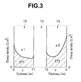
- FIG. 3 An example of charge distributions in the insulating layers is shown in Fig. 3 .
- a relatively large number of charges E are present in regions near the electrode layers and density distributions p are different in the upper insulating layer 15 and the lower insulating layer 12.
- Equation 2 An integrated value of a charge density distribution indicated by hatching in Fig. 3 is equivalent to the total charge amount ET.
- ET ⁇ 1 ⁇ 0 T ⁇ 1 ⁇ ⁇ 1 x ⁇ dx
- Equation 1 that takes into account the amounts of charges, the positions, and the dielectric constants indicates the effective charge amount EE, which is an accumulated charge amounts that affect the potential.
- the total charge amount ET1 of the lower insulating layer 12 and the total charge amount ET2 of the upper insulating layer 15 are different.
- Equation 1 an effective charge amount EE1 on the left side of Equation 1 was 4E-13C/cm and an effective charge amount EE2 on the right side was 4E-13C/cm.
- E-13 indicates 10 -13 .
- Equation 1 since Equation 1 was satisfied, the characteristics of the transducer 2 stabilized. Incidentally, because of presence of these effective charge amounts, both potential differences from the electrodes to a surface of the insulating film are 4.5 V.
- a publicly-known measuring apparatus can be used for measurement of a charge density distribution. Further, it is also possible to measure surface potential while removing a surface layer little by little. For the removal of the surface layer, a polishing method or an etching method can be used. For example, a silicon oxide layer is gradually etched by a buffered fluoric acid solution at speed of 100 nm/minute.
- the characteristics of the ultrasound transducer 2 according to the embodiment are stable because there is no influence of charge accumulation on the insulating layers.
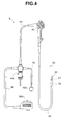
- an ultrasound endoscope 3 which is an ultrasound diagnostic apparatus, according to a second embodiment of the present invention is explained.
- An ultrasound transducer 2A included in an ultrasound transmitting and receiving section 30 of the ultrasound endoscope 3 is the same as the ultrasound transducer 2 according to the first embodiment. Therefore, explanation of the ultrasound transducer 2A is omitted.
- the ultrasound endoscope 3 includes an insertion section 42, an operation section 43, and a universal cord 44.
- An endoscope connector 44A is provided in a proximal end portion of the universal cord 44.
- An electric cable 45 connected to a camera control unit (not shown in the figure) via an electric connector 45A and an ultrasound cable 46 connected to an ultrasound observation apparatus (not shown in the figure) via an ultrasound connector 46A extend from the endoscope connector 44A.
- a rigid portion 47, a bending portion 48, and a flexible tube portion 49 are continuously provided.
- the ultrasound transmitting and receiving section 30 including the transducer 2 for transmitting and receiving ultrasound is provided.
- the ultrasound transmitting and receiving section 30 includes a transducer array 31, driving circuits 34, and an FPC 35.
- the FPC 35 is a flexible wiring board having flexibility and having mounting surfaces formed on both surfaces thereof.
- the FPC 35 is wound around in a substantially cylindrical shape with an axis substantially parallel to an insertion axis of the rigid portion 47 set as a center axis.
- the transducer array 31 includes one hundred twenty-eight transducer units 32 arrayed on the outer circumferential surface of the FPC 35 in a circumferential direction.
- the transducer units 32 have a substantially rectangular shape viewed from a normal direction of the outer circumferential surface of the FPC 35.
- the transducer units 32 are arrayed at an equal interval on the outer circumferential surface of the cylindrical FPC 35 with a latitudinal direction set as a circumferential direction.
- each of the transducer units 32 is configured by arraying sixty-four transducer elements 33.
- the transducer elements 33 have a substantially square shape viewed from the normal direction of the outer circumferential surface of the FPC 35.
- the transducer units 32 are one-dimensionally arrayed in a longitudinal direction of the transducer unit.
- each of the transducer elements 33 includes four ultrasound transducers 2A.
- the four transducers 2 are connected in parallel and transmit ultrasound of the same phase simultaneously with input of a driving signal.
- the driving circuits 34 for the transducer array 31 are mounted on an inner circumferential surface of the FPC 35, i.e., on the mounting surface on an opposite side of the mounting surface on which the respective transducer arrays 31 are mounted.
- the driving circuits 34 are electrically connected to plural signal electrodes 36 and plural ground electrodes 37 formed on the outer circumferential surface of the cylindrical FPC 35.
- the signal electrodes 36 and the ground electrodes 37 are inserted through the ultrasound cable 46 and connected to the ultrasound observation apparatus via the ultrasound connector 46A.
- the ultrasound transmitting and receiving section 30 simultaneously or alternately performs, with the transducer array 31, electronic radial scanning for radially transmitting and receiving ultrasound on a plane substantially orthogonal to the insertion axis of the rigid portion 47 and electronic sector scanning for radially transmitting and receiving ultrasound on a plane including the insertion axis of the rigid portion 47.
- the ultrasound endoscope 3 can perform three-dimensional ultrasound scanning.
- the ultrasound endoscope 3 includes the ultrasound transducer 2A that is not affected by accumulation in the insulating layers. Therefore, the characteristics of the ultrasound endoscope 3 are stable. It is possible to obtain a high-quality and satisfactory ultrasound diagnostic image.
- the ultrasound endoscope 3 performs the electronic radial scanning and the electronic sector scanning.
- a scanning system is not limited to these and may be linear scanning, convex scanning, or mechanical scanning.
- An ultrasound transmitting and receiving section in which plural transducer elements are one-dimensionally arrayed may be adopted.
- the ultrasound diagnostic apparatus may be an ultrasound probe or the like inserted through a treatment instrument through-hole of an endoscope and introduced into a body.
Landscapes
- Health & Medical Sciences (AREA)
- Life Sciences & Earth Sciences (AREA)
- Engineering & Computer Science (AREA)
- Medical Informatics (AREA)
- Surgery (AREA)
- Pathology (AREA)
- Radiology & Medical Imaging (AREA)
- Biophysics (AREA)
- Biomedical Technology (AREA)
- Heart & Thoracic Surgery (AREA)
- Physics & Mathematics (AREA)
- Molecular Biology (AREA)
- Nuclear Medicine, Radiotherapy & Molecular Imaging (AREA)
- Animal Behavior & Ethology (AREA)
- General Health & Medical Sciences (AREA)
- Public Health (AREA)
- Veterinary Medicine (AREA)
- Gynecology & Obstetrics (AREA)
- Mechanical Engineering (AREA)
- Ultra Sonic Daignosis Equipment (AREA)
- Transducers For Ultrasonic Waves (AREA)
Abstract
Description
- The present invention relates to a capacitance type ultrasound transducer and an ultrasound diagnostic apparatus including the capacitance type ultrasound transducer.
- An ultrasound diagnostic method for irradiating an inside of a body with ultrasound, converting a state of the inside of the body into an image from an echo signal of the ultrasound, and performing diagnosis is widespread. As one of ultrasound diagnostic apparatuses used in the ultrasound diagnostic method, there is an ultrasound endoscope. In the ultrasound endoscope, an ultrasound transducer is disposed at a distal end of an insertion section introduced into the body. The ultrasound transducer has a function of converting an electric signal into an ultrasound and transmitting the ultrasound to the inside of the body and receiving the ultrasound reflected in the body and converting the ultrasound into an electric signal.
- In the ultrasound transducer, a ceramic piezoelectric material, for example, PZT (lead zirconate titanate) is mainly used. On the other hand, as disclosed in Japanese Patent Application Laid-Open Publication No.
2009-55474 - Embodiments of the present invention have an objective to provide an ultrasound transducer with stable characteristics and an ultrasound diagnostic apparatus with stable characteristics.
- An ultrasound transducer according to an aspect of the present invention includes a substrate and a lower electrode layer, a lower insulating layer, an upper insulating layer, and an upper electrode layer laminated in order on the substrate. The lower insulating layer and the upper insulating layer are arranged to be opposed to each other via an air gap section. The upper insulating film and the lower insulating film are different in at least one of a material and thickness and satisfy Equation 1 below.

where, K1 represents a relative dielectric constant of the lower insulating layer, K2 represents a relative dielectric constant of the upper insulating layer, T1 represents layer thickness of the lower insulating layer, T2 represents layer thickness of the upper insulating layer, ρ1(x) represents a charge density distribution in the lower insulating layer (x represents a distance from the lower electrode layer), and ρ2(y) represents a charge density distribution in the upper insulating layer (y represents a distance from the upper electrode layer). - An ultrasound diagnostic apparatus according to another aspect of the present invention includes the ultrasound transducer explained above.
-
-
Fig. 1 is a diagram for explaining a sectional structure of an ultrasound transducer according to a first embodiment; -
Fig. 2 is a diagram for explaining, for example, arrangement of opposed electrodes of the ultrasound transducer according to the first embodiment; -
Fig. 3 is a diagram for explaining a charge distribution of an insulating layer of the ultrasound transducer according to the first embodiment; -
Fig. 4 is a diagram for explaining an ultrasound endoscope according to a second embodiment; -
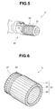
Fig. 5 is a diagram for explaining a distal end portion of the ultrasound endoscope according to the second embodiment; -
Fig. 6 is a diagram for explaining an ultrasound transmitting and receiving section of the ultrasound endoscope according to the second embodiment; and -
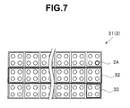
Fig. 7 is a diagram for explaining an ultrasound transducer of the ultrasound endoscope according to the second embodiment. - An
ultrasound transducer 2 according to a first embodiment of the present invention is explained below. Figures referred to below are schematic diagrams for explanation in which a scale and the like are different for each member. - As shown in
Fig. 1 , an ultrasound transducer (hereinafter referred to as "transducer") 2 includes asubstrate 10 and alower electrode layer 11, a lowerinsulating layer 12, agap layer 14, an upperinsulating layer 15, and anupper electrode layer 16 laminated on thesubstrate 10 in order. The lowerinsulating layer 12 and the upper insulatinglayer 15 are arranged to be opposed to each other via anair gap section 13. - In explanation of the laminated structure, concerning a vertical relation of the respective layers, a direction away from a surface of the
substrate 10 in a normal direction is represented as upper direction. For example, inFig. 1 , theupper electrode layer 16 is disposed above thelower electrode layer 11. - The
transducer 2 of a capacitance type transmits and receives ultrasound according to a change in a distance between theupper electrode layer 16 and thelower electrode layer 11, i.e., vibration of amembrane 18 including theupper electrode layer 16 and the upperinsulating layer 15. A protectinglayer 17 may be arranged on theupper electrode layer 16 to form themembrane 18 including the protectinglayer 17. - The
air gap section 13 forms a space for themembrane 18 to vibrate. As explained below, a shape of thelower electrode layer 11, theair gap section 13, and theupper electrode layer 16 observed from above is not specifically limited. However, a circular shape or the like can be applied as the shape. A material of thesubstrate 10 is not specifically limited. However, examples of the material include a low-resistance silicon wafer having electric conductivity. An insulating layer (not shown in the figure) may be formed on the surface of thesubstrate 10. - Examples of the
lower electrode layer 11 include MO (molybdenum), W (tungsten), Ti (titanium), Ta (tantalum), Al (aluminum), or Cu (copper). Thelower electrode layer 11 may be a multilayer structure formed by laminating two or more kinds of conductive materials. - On the
lower electrode layer 11, the lowerinsulating layer 12 is formed to cover thelower electrode layer 11. The lowerinsulating layer 12 is formed by, for example, a plasma CVD method. Examples of the lowerinsulating layer 12 include a silicon oxide layer, a silicon nitride layer, hafnium nitride (HfN), or hafnium oxynitride (HfON). However, as explained below, a material and layer thickness of the lowerinsulating layer 12 are determined in a relation with the upper insulatinglayer 15. Thegap layer 14 that forms theair gap section 13 is formed on the lowerinsulating layer 12. A shape of thegap layer 14 is determined as appropriate according to a shape of the membrane. - The upper insulating
layer 15 is formed on thegap layer 14. As the upperinsulating layer 15, a material same as the material of the lowerinsulating layer 12 can be formed by a method same as a method of forming the lowerinsulating layer 12. - The upper
insulating layer 15 and the lowerinsulating layer 12 are different in at least one of the material and the layer thickness. For example, when the upperinsulating layer 15 and the lowerinsulating layer 12 are different in the material, thelower insulating layer 12 is a silicon oxide layer excellent in heat resistance having layer thickness of 500 nm and the upper insulatinglayer 15 is a silicon nitride layer having layer thickness of 500 nm. When the upperinsulating layer 15 and thelower insulating layer 12 are different in the layer thickness, the lowerinsulating layer 12 is a silicon oxide layer having layer thickness of 150 nm and the upperinsulating layer 15 is a silicon oxide layer having layer thickness of 500 nm thicker than thelower insulating layer 12. When the upperinsulating layer 15 and thelower insulating layer 12 are different in the material and the layer thickness, the lowerinsulating layer 12 is a silicon oxide layer having layer thickness of 150 nm and the upperinsulating layer 15 is a silicon nitride layer having layer thickness of 500 nm. - As the material of the upper
insulating layer 15 and the lowerinsulating layer 12, an organic insulating material such as fluorine resin, polyimide, epoxy resin, or polyparaxylylene resin may be used. - Between the lower
insulating layer 12 and the upper insulatinglayer 15, theair gap section 13 in an atmospheric pressure, pressurized, or depressurized state is formed by thegap layer 14. The depressurized state indicates a state in which pressure is lower than the atmospheric pressure and includes a so-called vacuum state as well. Theair gap section 13 is formed in a substantially columnar shape and is provided substantially concentrically with thelower electrode layer 11 viewed from above. - The
upper electrode layer 16 is formed on the upper insulatinglayer 15. Theupper electrode layer 16 is provided substantially concentrically with thelower electrode layer 11 viewed from above, i.e., in a position opposed to thelower electrode layer 11. Theupper electrode layer 16 is formed by, for example, forming an Al film with a sputtering method and patterning the Al film. Thetransducer 2 has a substantially circular shape viewed from above. However, thetransducer 2 may be formed in, for example, a regular hexagonal shape or a rectangular shape. - A material forming the
upper electrode layer 16 may be, for example, Cu, W, Ti, or Ta. Theupper electrode layer 16 may have a multilayer structure formed by laminating two or more kinds of conductive materials. - The protecting
layer 17 is formed on theupper electrode layer 16. The protectinglayer 17 is, for example, a silicon nitride layer formed by the plasma CVD method. The protectinglayer 17 may be a silicon oxide layer, hafnium nitride (HfN) layer, a hafnium oxynitride (HfON) layer, or the like. - Although not shown in the figure, a layer formed of resin such as polyparaxylylene resin or polyimide having water resistance, chemical resistance, and the like and excellent in biocompatibility and electric insulation may be formed on the protecting
layer 17. - In general, the layer thicknesses and the like of the lower insulating
layer 12 and the upper insulatinglayer 15 are determined on the basis of specifications such as a frequency of ultrasound to be transmitted and received, an output, ultrasound reception sensitivity, and dielectric strength voltage. However, thetransducer 2 of this application further satisfies Equation 1 below.
- As shown in
Figs. 2 and3 , K1 represents a relative dielectric constant of the lower insulatinglayer 12, K2 represents a relative dielectric constant of the upper insulatinglayer 15, T1represents layer thickness of the lower insulatinglayer 12, T2 represents layer thickness of the upper insulatinglayer 15, ρ1(x) represents a charge density distribution in the lower insulating layer 12 (x represents a distance from the lower electrode layer), and ρ2(y) represents a charge density distribution in the upper insulating layer 15 (y represents a distance from the upper electrode layer). Amounts on both sides of Equation 1 are named as effective charge amounts (EE). - When a driving signal is applied to the ultrasound transducer, if an applied bias with which an electric current flows to an insulating film is used, charges are accumulated in the lower insulating layer and the upper insulating layer. In other words, values of ρ1 and p2 change. However, the values of ρ1 and p2 change while always keeping a proportional relation. An applied bias with which an electric current does not flow to the insulating film may be used or the values of ρ1 and p2 may be prevented from changing during driving of the ultrasound transducer. For example, a driving voltage may be reduced, the membrane may be hardened, a space between the upper insulating
layer 15 and the lower insulatinglayer 12 may be increased, or an obstacle for contact prevention may be disposed in the cavity to prevent the upper insulatinglayer 15 and the lower insulatinglayer 12 from coming into contact with each other during the driving. Examples of a method of hardening the membrane include a method of adjusting thickness and a diameter of the insulating film. - An example of charge distributions in the insulating layers is shown in
Fig. 3 . In the example shown inFig. 3 , a relatively large number of charges E are present in regions near the electrode layers and density distributions p are different in the upper insulatinglayer 15 and the lower insulatinglayer 12. - The inventor found as a result of extensive studies that what affects characteristics of the
transducer 2 is not a total charge amount ET, i.e., a total charge amount in a layer and that a charge density distribution and the like are important factors. - An integrated value of a charge density distribution indicated by hatching in
Fig. 3 is equivalent to the total charge amount ET. For example, a total charge amount ET1 of the lower insulatinglayer 12 is indicated byEquation 2 below.
- However, even if the total charge amount ET1 of the lower insulating
layer 12 and a total charge amount ET2 of the upper insulatinglayer 15 were the same, the characteristics of thetransducer 2 did not stabilize. - This is because the charges E in positions close to the electrode layers and the charges E in positions far from the electrode layers had different influences on the characteristics of the
transducer 2. Therefore, thicknesses of the insulating layers related to the characteristics of the transducer. Further, relative dielectric constants K of the electrode layers also contributed to the characteristics of the transducer. - It was confirmed that a product of distances from the electrode layers, in other words, positions (x, y) in a layer thickness direction of the insulating layers and the charges E present in the positions and the relative dielectric constants K of the respective electrode layers affected the characteristics of the
transducer 2. For example, even if the number of electrons (charges) present near the electrode layers is large, influences on potential are small. Equation 1 that takes into account the amounts of charges, the positions, and the dielectric constants indicates the effective charge amount EE, which is an accumulated charge amounts that affect the potential. - In other words, when Equation 1 is satisfied, since the influences of the charges on the potential are equivalent to each other, the characteristics of the
transducer 2 stabilize. - For example, when silicon oxide (SiO2) having layer thickness of 200 nm was used as the lower insulating
layer 12 and K1=4.0, a total charge amount ET1 indicated byEquation 2 was 8E-8C/cm2. On the other hand, when the upper insulatinglayer 15 was silicon nitride (Si3N4) having layer thickness of 500 nm and K2=8.0, a total charge amount ET2 indicated byEquation 2 was 6.4E-8C/cm2. - In short, the total charge amount ET1 of the lower insulating
layer 12 and the total charge amount ET2 of the upper insulatinglayer 15 are different. - However, in this case, an effective charge amount EE1 on the left side of Equation 1 was 4E-13C/cm and an effective charge amount EE2 on the right side was 4E-13C/cm. "E-13" indicates 10-13.
- Specifically, since Equation 1 was satisfied, the characteristics of the
transducer 2 stabilized. Incidentally, because of presence of these effective charge amounts, both potential differences from the electrodes to a surface of the insulating film are 4.5 V. - For measurement of a charge density distribution, a publicly-known measuring apparatus can be used. Further, it is also possible to measure surface potential while removing a surface layer little by little. For the removal of the surface layer, a polishing method or an etching method can be used. For example, a silicon oxide layer is gradually etched by a buffered fluoric acid solution at speed of 100 nm/minute.
- As explained above, the characteristics of the
ultrasound transducer 2 according to the embodiment are stable because there is no influence of charge accumulation on the insulating layers. - To adjust the effective charge amount EE to satisfy Equation 1, it is desirable from viewpoints of easiness of a manufacturing method and easiness of control to change the layer thicknesses of the lower insulating
layer 12 and the upper insulatinglayer 15. - Next, an
ultrasound endoscope 3, which is an ultrasound diagnostic apparatus, according to a second embodiment of the present invention is explained. Anultrasound transducer 2A included in an ultrasound transmitting and receivingsection 30 of theultrasound endoscope 3 is the same as theultrasound transducer 2 according to the first embodiment. Therefore, explanation of theultrasound transducer 2A is omitted. - As shown in
Fig. 4 , theultrasound endoscope 3 includes aninsertion section 42, anoperation section 43, and auniversal cord 44. Anendoscope connector 44A is provided in a proximal end portion of theuniversal cord 44. Anelectric cable 45 connected to a camera control unit (not shown in the figure) via anelectric connector 45A and anultrasound cable 46 connected to an ultrasound observation apparatus (not shown in the figure) via anultrasound connector 46A extend from theendoscope connector 44A. - In the
insertion section 42, arigid portion 47, a bendingportion 48, and aflexible tube portion 49 are continuously provided. - On a distal end side of the
rigid portion 47, the ultrasound transmitting and receivingsection 30 including thetransducer 2 for transmitting and receiving ultrasound is provided. - As shown in
Figs. 5 and 6 , the ultrasound transmitting and receivingsection 30 includes atransducer array 31, drivingcircuits 34, and anFPC 35. TheFPC 35 is a flexible wiring board having flexibility and having mounting surfaces formed on both surfaces thereof. TheFPC 35 is wound around in a substantially cylindrical shape with an axis substantially parallel to an insertion axis of therigid portion 47 set as a center axis. - On an outer circumferential surface of the
cylindrical FPC 35, the two-dimensional ultrasound transducer array (hereinafter referred to as "transducer array") 31 is provided. Thetransducer array 31 includes one hundred twenty-eighttransducer units 32 arrayed on the outer circumferential surface of theFPC 35 in a circumferential direction. Thetransducer units 32 have a substantially rectangular shape viewed from a normal direction of the outer circumferential surface of theFPC 35. Thetransducer units 32 are arrayed at an equal interval on the outer circumferential surface of thecylindrical FPC 35 with a latitudinal direction set as a circumferential direction. - As shown in
Fig. 7 , each of thetransducer units 32 is configured by arraying sixty-fourtransducer elements 33. Thetransducer elements 33 have a substantially square shape viewed from the normal direction of the outer circumferential surface of theFPC 35. Thetransducer units 32 are one-dimensionally arrayed in a longitudinal direction of the transducer unit. - Further, each of the
transducer elements 33 includes fourultrasound transducers 2A. The fourtransducers 2 are connected in parallel and transmit ultrasound of the same phase simultaneously with input of a driving signal. - On an inner circumferential surface of the
FPC 35, i.e., on the mounting surface on an opposite side of the mounting surface on which therespective transducer arrays 31 are mounted, the drivingcircuits 34 for thetransducer array 31 are mounted. The drivingcircuits 34 are electrically connected toplural signal electrodes 36 andplural ground electrodes 37 formed on the outer circumferential surface of thecylindrical FPC 35. - The
signal electrodes 36 and theground electrodes 37 are inserted through theultrasound cable 46 and connected to the ultrasound observation apparatus via theultrasound connector 46A. - The ultrasound transmitting and receiving
section 30 simultaneously or alternately performs, with thetransducer array 31, electronic radial scanning for radially transmitting and receiving ultrasound on a plane substantially orthogonal to the insertion axis of therigid portion 47 and electronic sector scanning for radially transmitting and receiving ultrasound on a plane including the insertion axis of therigid portion 47. In other words, theultrasound endoscope 3 can perform three-dimensional ultrasound scanning. - The
ultrasound endoscope 3 includes theultrasound transducer 2A that is not affected by accumulation in the insulating layers. Therefore, the characteristics of theultrasound endoscope 3 are stable. It is possible to obtain a high-quality and satisfactory ultrasound diagnostic image. - The
ultrasound endoscope 3 performs the electronic radial scanning and the electronic sector scanning. However, a scanning system is not limited to these and may be linear scanning, convex scanning, or mechanical scanning. An ultrasound transmitting and receiving section in which plural transducer elements are one-dimensionally arrayed may be adopted. - The ultrasound diagnostic apparatus may be an ultrasound probe or the like inserted through a treatment instrument through-hole of an endoscope and introduced into a body.
- The present invention is not limited to the above-described embodiments or modifications but combinations, various changes, alterations, etc. of the embodiments or modifications may be made within the scope not changing the gist of the present invention.
- The present application is filed claiming the priority of Japanese Patent Application No.
2011-066482
Claims (8)
- An ultrasound transducer comprising: a substrate; and a lower electrode layer, a lower insulating layer, an upper insulating layer, and an upper electrode layer laminated in order on the substrate, wherein
the lower insulating layer and the upper insulating layer are arranged to be opposed to each other via an air gap section, are different in at least one of a material and thickness, and satisfy Equation 1 below:
where, K1 represents a relative dielectric constant of the lower insulating layer, K2 represents a relative dielectric constant of the upper insulating layer, T1represents layer thickness of the lower insulating layer, T2 represents layer thickness of the upper insulating layer, ρ1(x) represents a charge density distribution in the lower insulating layer (x represents a distance from the lower electrode layer), and ρ2(y) represents a charge density distribution in the upper insulating layer (y represents a distance from the upper electrode layer). - The ultrasound transducer according to claim 1, wherein the layer thicknesses of the lower insulating layer and the upper insulating layer made of a same material are different.
- The ultrasound transducer according to claim 2, wherein the lower insulating layer and the upper insulating layer are different in the material and the layer thickness.
- The ultrasound transducer according to claim 3, wherein the lower insulating layer and the upper insulating layer do not come into contact with each other during driving, and the ρ1(x) and the p2(x) do not change even if a driving signal is applied to the lower electrode layer and the upper electrode layer.
- An ultrasound diagnostic apparatus comprising an ultrasound transducer including: a substrate; and a lower electrode layer, a lower insulating layer, an upper insulating layer, and an upper electrode layer laminated in order on the substrate, wherein
the lower insulating layer and the upper insulating layer are arranged to be opposed to each other via an air gap section, are different in at least one of a material and thickness, and satisfy Equation 1 below:
where, K1 represents a relative dielectric constant of the lower insulating layer, K2 represents a relative dielectric constant of the upper insulating layer, T1 represents layer thickness of the lower insulating layer, T2 represents layer thickness of the upper insulating layer, ρ1(x) represents a charge density distribution in the lower insulating layer (x represents a distance from the lower electrode layer), and ρ2(y) represents a charge density distribution in the upper insulating layer (y represents a distance from the upper electrode layer). - The ultrasound diagnostic apparatus according to claim 5, wherein, in the ultrasound transducer, the layer thicknesses of the lower insulating layer and the upper insulating layer made of a same material are different.
- The ultrasound diagnostic apparatus according to claim 6, wherein, in the ultrasound transducer, the lower insulating layer and the upper insulating layer are different in the material and the layer thickness.
- The ultrasound diagnostic apparatus according to claim 7, wherein, in the ultrasound transducer, the lower insulating layer and the upper insulating layer do not come into contact with each other during driving, and the ρ1(x) and the p2(x) do not change even if a driving signal is applied to the lower electrode layer and the upper electrode layer.
Applications Claiming Priority (2)
| Application Number | Priority Date | Filing Date | Title |
|---|---|---|---|
| JP2011066482 | 2011-03-24 | ||
| PCT/JP2011/076825 WO2012127737A1 (en) | 2011-03-24 | 2011-11-21 | Ultrasonic oscillator and ultrasonic diagnosis device |
Publications (3)
| Publication Number | Publication Date |
|---|---|
| EP2595412A1 true EP2595412A1 (en) | 2013-05-22 |
| EP2595412A4 EP2595412A4 (en) | 2013-07-03 |
| EP2595412B1 EP2595412B1 (en) | 2015-10-21 |
Family
ID=46878925
Family Applications (1)
| Application Number | Title | Priority Date | Filing Date |
|---|---|---|---|
| EP11861763.8A Active EP2595412B1 (en) | 2011-03-24 | 2011-11-21 | Ultrasound transducer and ultrasound diagnostic apparatus |
Country Status (4)
| Country | Link |
|---|---|
| US (1) | US8512251B2 (en) |
| EP (1) | EP2595412B1 (en) |
| JP (1) | JP5153972B2 (en) |
| WO (1) | WO2012127737A1 (en) |
Families Citing this family (9)
| Publication number | Priority date | Publication date | Assignee | Title |
|---|---|---|---|---|
| CN106163415B (en) | 2014-04-10 | 2020-04-14 | 皇家飞利浦有限公司 | Needle with piezoelectric polymer sensor |
| JP2016101417A (en) * | 2014-11-28 | 2016-06-02 | キヤノン株式会社 | Capacitance-type acoustic wave transducer and subject information acquisition apparatus with the same |
| WO2017145514A1 (en) * | 2016-02-23 | 2017-08-31 | 株式会社日立製作所 | Ultrasonic probe and method for producing same |
| US12588894B2 (en) | 2017-03-07 | 2026-03-31 | Koninklijke Philips N.V. | Imaging assembly for intraluminal imaging |
| JP7085636B2 (en) * | 2018-10-19 | 2022-06-16 | オリンパス株式会社 | Ultrasonic probe and ultrasonic endoscope |
| JP2019075831A (en) * | 2019-02-12 | 2019-05-16 | キヤノン株式会社 | Capacitance-type acoustic wave transducer and subject information acquisition apparatus with the same |
| FR3096857B1 (en) * | 2019-05-29 | 2021-06-25 | Aer | MINIATURIZED ULTRASONIC CAPACITIVE ELECTROACOUSTIC TRANSDUCER OPERATING AT HIGH VOLTAGE |
| US11738369B2 (en) | 2020-02-17 | 2023-08-29 | GE Precision Healthcare LLC | Capactive micromachined transducer having a high contact resistance part |
| JP7324181B2 (en) * | 2020-09-08 | 2023-08-09 | 富士フイルム株式会社 | ultrasound endoscope |
Family Cites Families (8)
| Publication number | Priority date | Publication date | Assignee | Title |
|---|---|---|---|---|
| EP1907133A4 (en) * | 2005-06-17 | 2012-05-09 | Kolo Technologies Inc | MICROELECTROMECHANICAL TRANSDUCER HAVING AN ISOLATION EXTENSION |
| JP4271252B2 (en) * | 2006-10-12 | 2009-06-03 | オリンパスメディカルシステムズ株式会社 | Ultrasonic transducer cell, ultrasonic transducer element, ultrasonic transducer array, and ultrasonic diagnostic apparatus |
| JP2008099036A (en) | 2006-10-12 | 2008-04-24 | Olympus Medical Systems Corp | Ultrasonic transducer, ultrasonic probe and ultrasonic diagnostic apparatus |
| JP5329408B2 (en) | 2007-07-11 | 2013-10-30 | 株式会社日立メディコ | Ultrasonic probe and ultrasonic diagnostic apparatus |
| US8047995B2 (en) * | 2007-08-28 | 2011-11-01 | Olympus Medical Systems Corp. | Ultrasonic transducer, method of manufacturing ultrasonic transducer, ultrasonic diagnostic apparatus, and ultrasonic microscope |
| JP4774394B2 (en) * | 2007-08-28 | 2011-09-14 | オリンパスメディカルシステムズ株式会社 | Ultrasonic transducer, ultrasonic transducer manufacturing method, ultrasonic diagnostic apparatus, and ultrasonic microscope |
| JP5019997B2 (en) | 2007-08-28 | 2012-09-05 | オリンパスメディカルシステムズ株式会社 | Ultrasonic transducer, ultrasonic diagnostic apparatus and ultrasonic microscope |
| JP2011066482A (en) | 2009-09-15 | 2011-03-31 | Sanyo Electric Co Ltd | Drive circuit |
-
2011
- 2011-11-21 JP JP2012543379A patent/JP5153972B2/en active Active
- 2011-11-21 EP EP11861763.8A patent/EP2595412B1/en active Active
- 2011-11-21 WO PCT/JP2011/076825 patent/WO2012127737A1/en not_active Ceased
-
2012
- 2012-09-13 US US13/614,168 patent/US8512251B2/en active Active
Also Published As
| Publication number | Publication date |
|---|---|
| WO2012127737A1 (en) | 2012-09-27 |
| JP5153972B2 (en) | 2013-02-27 |
| US8512251B2 (en) | 2013-08-20 |
| EP2595412A4 (en) | 2013-07-03 |
| JPWO2012127737A1 (en) | 2014-07-24 |
| US20130018269A1 (en) | 2013-01-17 |
| EP2595412B1 (en) | 2015-10-21 |
Similar Documents
| Publication | Publication Date | Title |
|---|---|---|
| EP2595412B1 (en) | Ultrasound transducer and ultrasound diagnostic apparatus | |
| EP3079838B1 (en) | Flexible micromachined transducer device and method for fabricating same | |
| US7940603B2 (en) | Ultrasonic transducer cell | |
| US20100262014A1 (en) | Ultrasound Scanner Built with Capacitive Micromachined Ultrasonic Transducers (CMUTS) | |
| EP3174643B1 (en) | Intravascular ultrasound imaging apparatus, interface architecture, and method of manufacturing | |
| EP2030698B1 (en) | Ultrasonic transducer, method of manufacturing ultrasonic transducer, ultrasonic diagnostic apparatus, and ultrasonic microscope | |
| JP4774393B2 (en) | Ultrasonic transducer, ultrasonic diagnostic apparatus and ultrasonic microscope | |
| US20080089180A1 (en) | Ultrasonic transducer, ultrasonic probe, and ultrasonic diagnostic apparatus | |
| US20090204004A1 (en) | Ultrasound transducer and ultrasound diagnostic apparatus | |
| US20200101492A1 (en) | Capacitive transducer, manufacturing method thereof, and image forming apparatus | |
| US9629609B2 (en) | Ultrasound element and ultrasound endoscope | |
| JP4891182B2 (en) | Ultrasonic transducer, ultrasonic diagnostic apparatus and ultrasonic microscope | |
| EP2775736A1 (en) | Ultrasonic oscillator element and ultrasonic endoscope | |
| EP2733961B1 (en) | Ultrasonic element, and ultrasonic endoscope | |
| US20210291231A1 (en) | Electromechanical transducer element, ultrasonic transducer, ultrasonic probe, ultrasonic diagnostic apparatus, and method for manufacturing electromechanical transducer element |
Legal Events
| Date | Code | Title | Description |
|---|---|---|---|
| PUAI | Public reference made under article 153(3) epc to a published international application that has entered the european phase |
Free format text: ORIGINAL CODE: 0009012 |
|
| 17P | Request for examination filed |
Effective date: 20130214 |
|
| AK | Designated contracting states |
Kind code of ref document: A1 Designated state(s): AL AT BE BG CH CY CZ DE DK EE ES FI FR GB GR HR HU IE IS IT LI LT LU LV MC MK MT NL NO PL PT RO RS SE SI SK SM TR |
|
| A4 | Supplementary search report drawn up and despatched |
Effective date: 20130605 |
|
| RIC1 | Information provided on ipc code assigned before grant |
Ipc: H04R 19/00 20060101AFI20130530BHEP Ipc: A61B 8/12 20060101ALI20130530BHEP |
|
| DAX | Request for extension of the european patent (deleted) | ||
| 17Q | First examination report despatched |
Effective date: 20140718 |
|
| GRAP | Despatch of communication of intention to grant a patent |
Free format text: ORIGINAL CODE: EPIDOSNIGR1 |
|
| INTG | Intention to grant announced |
Effective date: 20150604 |
|
| RIN1 | Information on inventor provided before grant (corrected) |
Inventor name: YOSHIDA, SATOSHI Inventor name: MATSUMOTO, KAZUYA Inventor name: KARAKI, KAZUHISA Inventor name: WAKABAYASHI, KATSUHIRO Inventor name: HIRAOKA, JIN Inventor name: HASEGAWA, MAMORU |
|
| GRAS | Grant fee paid |
Free format text: ORIGINAL CODE: EPIDOSNIGR3 |
|
| GRAA | (expected) grant |
Free format text: ORIGINAL CODE: 0009210 |
|
| RIN1 | Information on inventor provided before grant (corrected) |
Inventor name: YOSHIDA, SATOSHI Inventor name: MATSUMOTO, KAZUYA Inventor name: HIRAOKA, JIN Inventor name: WAKABAYASHI, KATSUHIRO Inventor name: KARAKI, KAZUHISA Inventor name: HASEGAWA, MAMORU |
|
| AK | Designated contracting states |
Kind code of ref document: B1 Designated state(s): AL AT BE BG CH CY CZ DE DK EE ES FI FR GB GR HR HU IE IS IT LI LT LU LV MC MK MT NL NO PL PT RO RS SE SI SK SM TR |
|
| REG | Reference to a national code |
Ref country code: GB Ref legal event code: FG4D Ref country code: NL Ref legal event code: MP Effective date: 20151021 |
|
| RAP2 | Party data changed (patent owner data changed or rights of a patent transferred) |
Owner name: OLYMPUS CORPORATION |
|
| REG | Reference to a national code |
Ref country code: CH Ref legal event code: EP |
|
| REG | Reference to a national code |
Ref country code: AT Ref legal event code: REF Ref document number: 757313 Country of ref document: AT Kind code of ref document: T Effective date: 20151115 |
|
| REG | Reference to a national code |
Ref country code: IE Ref legal event code: FG4D |
|
| REG | Reference to a national code |
Ref country code: DE Ref legal event code: R096 Ref document number: 602011020918 Country of ref document: DE |
|
| REG | Reference to a national code |
Ref country code: LT Ref legal event code: MG4D |
|
| REG | Reference to a national code |
Ref country code: AT Ref legal event code: MK05 Ref document number: 757313 Country of ref document: AT Kind code of ref document: T Effective date: 20151021 |
|
| PG25 | Lapsed in a contracting state [announced via postgrant information from national office to epo] |
Ref country code: HR Free format text: LAPSE BECAUSE OF FAILURE TO SUBMIT A TRANSLATION OF THE DESCRIPTION OR TO PAY THE FEE WITHIN THE PRESCRIBED TIME-LIMIT Effective date: 20151021 Ref country code: ES Free format text: LAPSE BECAUSE OF FAILURE TO SUBMIT A TRANSLATION OF THE DESCRIPTION OR TO PAY THE FEE WITHIN THE PRESCRIBED TIME-LIMIT Effective date: 20151021 Ref country code: IT Free format text: LAPSE BECAUSE OF FAILURE TO SUBMIT A TRANSLATION OF THE DESCRIPTION OR TO PAY THE FEE WITHIN THE PRESCRIBED TIME-LIMIT Effective date: 20151021 Ref country code: IS Free format text: LAPSE BECAUSE OF FAILURE TO SUBMIT A TRANSLATION OF THE DESCRIPTION OR TO PAY THE FEE WITHIN THE PRESCRIBED TIME-LIMIT Effective date: 20160221 Ref country code: LT Free format text: LAPSE BECAUSE OF FAILURE TO SUBMIT A TRANSLATION OF THE DESCRIPTION OR TO PAY THE FEE WITHIN THE PRESCRIBED TIME-LIMIT Effective date: 20151021 Ref country code: NL Free format text: LAPSE BECAUSE OF FAILURE TO SUBMIT A TRANSLATION OF THE DESCRIPTION OR TO PAY THE FEE WITHIN THE PRESCRIBED TIME-LIMIT Effective date: 20151021 Ref country code: NO Free format text: LAPSE BECAUSE OF FAILURE TO SUBMIT A TRANSLATION OF THE DESCRIPTION OR TO PAY THE FEE WITHIN THE PRESCRIBED TIME-LIMIT Effective date: 20160121 |
|
| PG25 | Lapsed in a contracting state [announced via postgrant information from national office to epo] |
Ref country code: AT Free format text: LAPSE BECAUSE OF FAILURE TO SUBMIT A TRANSLATION OF THE DESCRIPTION OR TO PAY THE FEE WITHIN THE PRESCRIBED TIME-LIMIT Effective date: 20151021 Ref country code: RS Free format text: LAPSE BECAUSE OF FAILURE TO SUBMIT A TRANSLATION OF THE DESCRIPTION OR TO PAY THE FEE WITHIN THE PRESCRIBED TIME-LIMIT Effective date: 20151021 Ref country code: FI Free format text: LAPSE BECAUSE OF FAILURE TO SUBMIT A TRANSLATION OF THE DESCRIPTION OR TO PAY THE FEE WITHIN THE PRESCRIBED TIME-LIMIT Effective date: 20151021 Ref country code: LV Free format text: LAPSE BECAUSE OF FAILURE TO SUBMIT A TRANSLATION OF THE DESCRIPTION OR TO PAY THE FEE WITHIN THE PRESCRIBED TIME-LIMIT Effective date: 20151021 Ref country code: PL Free format text: LAPSE BECAUSE OF FAILURE TO SUBMIT A TRANSLATION OF THE DESCRIPTION OR TO PAY THE FEE WITHIN THE PRESCRIBED TIME-LIMIT Effective date: 20151021 Ref country code: GR Free format text: LAPSE BECAUSE OF FAILURE TO SUBMIT A TRANSLATION OF THE DESCRIPTION OR TO PAY THE FEE WITHIN THE PRESCRIBED TIME-LIMIT Effective date: 20160122 Ref country code: PT Free format text: LAPSE BECAUSE OF FAILURE TO SUBMIT A TRANSLATION OF THE DESCRIPTION OR TO PAY THE FEE WITHIN THE PRESCRIBED TIME-LIMIT Effective date: 20160222 Ref country code: SE Free format text: LAPSE BECAUSE OF FAILURE TO SUBMIT A TRANSLATION OF THE DESCRIPTION OR TO PAY THE FEE WITHIN THE PRESCRIBED TIME-LIMIT Effective date: 20151021 |
|
| REG | Reference to a national code |
Ref country code: CH Ref legal event code: PL |
|
| REG | Reference to a national code |
Ref country code: DE Ref legal event code: R097 Ref document number: 602011020918 Country of ref document: DE |
|
| PG25 | Lapsed in a contracting state [announced via postgrant information from national office to epo] |
Ref country code: MC Free format text: LAPSE BECAUSE OF FAILURE TO SUBMIT A TRANSLATION OF THE DESCRIPTION OR TO PAY THE FEE WITHIN THE PRESCRIBED TIME-LIMIT Effective date: 20151021 Ref country code: CH Free format text: LAPSE BECAUSE OF NON-PAYMENT OF DUE FEES Effective date: 20151130 Ref country code: LI Free format text: LAPSE BECAUSE OF NON-PAYMENT OF DUE FEES Effective date: 20151130 Ref country code: CZ Free format text: LAPSE BECAUSE OF FAILURE TO SUBMIT A TRANSLATION OF THE DESCRIPTION OR TO PAY THE FEE WITHIN THE PRESCRIBED TIME-LIMIT Effective date: 20151021 |
|
| REG | Reference to a national code |
Ref country code: IE Ref legal event code: MM4A |
|
| PLBE | No opposition filed within time limit |
Free format text: ORIGINAL CODE: 0009261 |
|
| REG | Reference to a national code |
Ref country code: FR Ref legal event code: ST Effective date: 20160729 |
|
| STAA | Information on the status of an ep patent application or granted ep patent |
Free format text: STATUS: NO OPPOSITION FILED WITHIN TIME LIMIT |
|
| PG25 | Lapsed in a contracting state [announced via postgrant information from national office to epo] |
Ref country code: SM Free format text: LAPSE BECAUSE OF FAILURE TO SUBMIT A TRANSLATION OF THE DESCRIPTION OR TO PAY THE FEE WITHIN THE PRESCRIBED TIME-LIMIT Effective date: 20151021 Ref country code: RO Free format text: LAPSE BECAUSE OF FAILURE TO SUBMIT A TRANSLATION OF THE DESCRIPTION OR TO PAY THE FEE WITHIN THE PRESCRIBED TIME-LIMIT Effective date: 20151021 Ref country code: DK Free format text: LAPSE BECAUSE OF FAILURE TO SUBMIT A TRANSLATION OF THE DESCRIPTION OR TO PAY THE FEE WITHIN THE PRESCRIBED TIME-LIMIT Effective date: 20151021 Ref country code: EE Free format text: LAPSE BECAUSE OF FAILURE TO SUBMIT A TRANSLATION OF THE DESCRIPTION OR TO PAY THE FEE WITHIN THE PRESCRIBED TIME-LIMIT Effective date: 20151021 Ref country code: SK Free format text: LAPSE BECAUSE OF FAILURE TO SUBMIT A TRANSLATION OF THE DESCRIPTION OR TO PAY THE FEE WITHIN THE PRESCRIBED TIME-LIMIT Effective date: 20151021 |
|
| 26N | No opposition filed |
Effective date: 20160722 |
|
| GBPC | Gb: european patent ceased through non-payment of renewal fee |
Effective date: 20160121 |
|
| PG25 | Lapsed in a contracting state [announced via postgrant information from national office to epo] |
Ref country code: GB Free format text: LAPSE BECAUSE OF NON-PAYMENT OF DUE FEES Effective date: 20160121 Ref country code: IE Free format text: LAPSE BECAUSE OF NON-PAYMENT OF DUE FEES Effective date: 20151121 |
|
| PG25 | Lapsed in a contracting state [announced via postgrant information from national office to epo] |
Ref country code: FR Free format text: LAPSE BECAUSE OF NON-PAYMENT OF DUE FEES Effective date: 20151221 Ref country code: SI Free format text: LAPSE BECAUSE OF FAILURE TO SUBMIT A TRANSLATION OF THE DESCRIPTION OR TO PAY THE FEE WITHIN THE PRESCRIBED TIME-LIMIT Effective date: 20151021 |
|
| PG25 | Lapsed in a contracting state [announced via postgrant information from national office to epo] |
Ref country code: BE Free format text: LAPSE BECAUSE OF FAILURE TO SUBMIT A TRANSLATION OF THE DESCRIPTION OR TO PAY THE FEE WITHIN THE PRESCRIBED TIME-LIMIT Effective date: 20151021 |
|
| PG25 | Lapsed in a contracting state [announced via postgrant information from national office to epo] |
Ref country code: HU Free format text: LAPSE BECAUSE OF FAILURE TO SUBMIT A TRANSLATION OF THE DESCRIPTION OR TO PAY THE FEE WITHIN THE PRESCRIBED TIME-LIMIT; INVALID AB INITIO Effective date: 20111121 Ref country code: BG Free format text: LAPSE BECAUSE OF FAILURE TO SUBMIT A TRANSLATION OF THE DESCRIPTION OR TO PAY THE FEE WITHIN THE PRESCRIBED TIME-LIMIT Effective date: 20151021 |
|
| PG25 | Lapsed in a contracting state [announced via postgrant information from national office to epo] |
Ref country code: CY Free format text: LAPSE BECAUSE OF FAILURE TO SUBMIT A TRANSLATION OF THE DESCRIPTION OR TO PAY THE FEE WITHIN THE PRESCRIBED TIME-LIMIT Effective date: 20151021 |
|
| PG25 | Lapsed in a contracting state [announced via postgrant information from national office to epo] |
Ref country code: MT Free format text: LAPSE BECAUSE OF FAILURE TO SUBMIT A TRANSLATION OF THE DESCRIPTION OR TO PAY THE FEE WITHIN THE PRESCRIBED TIME-LIMIT Effective date: 20151021 |
|
| PG25 | Lapsed in a contracting state [announced via postgrant information from national office to epo] |
Ref country code: LU Free format text: LAPSE BECAUSE OF NON-PAYMENT OF DUE FEES Effective date: 20151121 |
|
| PG25 | Lapsed in a contracting state [announced via postgrant information from national office to epo] |
Ref country code: TR Free format text: LAPSE BECAUSE OF FAILURE TO SUBMIT A TRANSLATION OF THE DESCRIPTION OR TO PAY THE FEE WITHIN THE PRESCRIBED TIME-LIMIT Effective date: 20151021 Ref country code: MK Free format text: LAPSE BECAUSE OF FAILURE TO SUBMIT A TRANSLATION OF THE DESCRIPTION OR TO PAY THE FEE WITHIN THE PRESCRIBED TIME-LIMIT Effective date: 20151021 |
|
| PG25 | Lapsed in a contracting state [announced via postgrant information from national office to epo] |
Ref country code: AL Free format text: LAPSE BECAUSE OF FAILURE TO SUBMIT A TRANSLATION OF THE DESCRIPTION OR TO PAY THE FEE WITHIN THE PRESCRIBED TIME-LIMIT Effective date: 20151021 |
|
| P01 | Opt-out of the competence of the unified patent court (upc) registered |
Effective date: 20230528 |
|
| PGFP | Annual fee paid to national office [announced via postgrant information from national office to epo] |
Ref country code: DE Payment date: 20251119 Year of fee payment: 15 |