EP2593585B1 - Leveling of master electrode and substrate in ecpr, and a chuck therefor - Google Patents
Leveling of master electrode and substrate in ecpr, and a chuck therefor Download PDFInfo
- Publication number
- EP2593585B1 EP2593585B1 EP11745503.0A EP11745503A EP2593585B1 EP 2593585 B1 EP2593585 B1 EP 2593585B1 EP 11745503 A EP11745503 A EP 11745503A EP 2593585 B1 EP2593585 B1 EP 2593585B1
- Authority
- EP
- European Patent Office
- Prior art keywords
- chuck
- leveling
- teeth
- interaction surface
- plane
- Prior art date
- Legal status (The legal status is an assumption and is not a legal conclusion. Google has not performed a legal analysis and makes no representation as to the accuracy of the status listed.)
- Not-in-force
Links
Images

Classifications
-
- H—ELECTRICITY
- H10—SEMICONDUCTOR DEVICES; ELECTRIC SOLID-STATE DEVICES NOT OTHERWISE PROVIDED FOR
- H10P—GENERIC PROCESSES OR APPARATUS FOR THE MANUFACTURE OR TREATMENT OF DEVICES COVERED BY CLASS H10
- H10P72/00—Handling or holding of wafers, substrates or devices during manufacture or treatment thereof
- H10P72/70—Handling or holding of wafers, substrates or devices during manufacture or treatment thereof for supporting or gripping
- H10P72/76—Handling or holding of wafers, substrates or devices during manufacture or treatment thereof for supporting or gripping using mechanical means, e.g. clamps or pinches
- H10P72/7604—Handling or holding of wafers, substrates or devices during manufacture or treatment thereof for supporting or gripping using mechanical means, e.g. clamps or pinches the wafers being placed on a susceptor, stage or support
- H10P72/7611—Handling or holding of wafers, substrates or devices during manufacture or treatment thereof for supporting or gripping using mechanical means, e.g. clamps or pinches the wafers being placed on a susceptor, stage or support characterised by edge profile or support profile
-
- C—CHEMISTRY; METALLURGY
- C25—ELECTROLYTIC OR ELECTROPHORETIC PROCESSES; APPARATUS THEREFOR
- C25D—PROCESSES FOR THE ELECTROLYTIC OR ELECTROPHORETIC PRODUCTION OF COATINGS; ELECTROFORMING; APPARATUS THEREFOR
- C25D1/00—Electroforming
-
- C—CHEMISTRY; METALLURGY
- C25—ELECTROLYTIC OR ELECTROPHORETIC PROCESSES; APPARATUS THEREFOR
- C25D—PROCESSES FOR THE ELECTROLYTIC OR ELECTROPHORETIC PRODUCTION OF COATINGS; ELECTROFORMING; APPARATUS THEREFOR
- C25D17/00—Constructional parts, or assemblies thereof, of cells for electrolytic coating
- C25D17/06—Suspending or supporting devices for articles to be coated
-
- C—CHEMISTRY; METALLURGY
- C25—ELECTROLYTIC OR ELECTROPHORETIC PROCESSES; APPARATUS THEREFOR
- C25D—PROCESSES FOR THE ELECTROLYTIC OR ELECTROPHORETIC PRODUCTION OF COATINGS; ELECTROFORMING; APPARATUS THEREFOR
- C25D7/00—Electroplating characterised by the article coated
- C25D7/12—Semiconductors
- C25D7/123—Semiconductors first coated with a seed layer or a conductive layer
Definitions
- This invention pertains in general to the field of electrochemical pattern replication. More particularly the invention relates to a method for leveling a master electrode and a substrate in ECPR, and a chuck adapted therefore.
- Electroplating/electroetching is used for microelectronics in a wide range of applications, such as interconnects, components, waveguides, inductors, contact pads etc.
- electroplating/electroetching is suitable for applications involving production of micro and nano structures in single or multiple layers, fabrication of PWB (printed wiring boards), PCB (printed circuit boards), MEMS (micro electro mechanical systems), IC (integrated circuit) interconnects, above IC interconnects, sensors, flat panel displays, magnetic and optical storage devices, solar cells and other electronic devices. It can also be used for different types of structures in conductive polymers, structures in semiconductors, structures in metals, and others. Even 3D-structures in silicon, such as by formation of porous silicon, are possible.
- Chemical vapour deposition and physical vapour deposition are processes that may also be used for metallization, but electroplating/electroetching is often preferred since it is generally less expensive than other metallization processes and it can take place at ambient temperatures and at ambient pressures.
- Electroplating/electroetching of a work piece takes place in a reactor containing an electrolyte.
- An anode carrying the metal to be plated, is connected to a positive voltage.
- the anode is inert and the metal to be plated comes from the ions in the electrolyte.
- the conductivity of the work piece such as a semiconductor substrate, is generally too low to allow the structures to be plated to be connected through the substrate to backside contacts. Therefore, the structures to be plated first have to be provided with a conductive layer, such as a seed layer. Leads connect the pattern to finger contacts on the front side. The finger contacts are in turn connected to a negative voltage.
- the electroplating step is an electrolytic process where the metal is transferred from the anode, or from the ions in the electrolyte, to the conductive pattern (cathode) by the electrolyte and the applied electric field between the anode and the conductive layer on the work piece, which forms the cathode.
- ECPR plating/etching cells or cavities are formed between a master electrode and the substrate, said cavities being defined by a conductive surface on the master electrode, an insulating material, defining the pattern to be plated/etched, and the conductive surface of the substrate.
- a predeposited anode material has been arranged, normally through electrochemical plating, in the cavities.
- the master electrode and the substrate are put in close contact with each other in the presence of an electrolyte, suitable for the intended purpose, such that the electrolyte is "trapped" in the ECPR plating/etching cavities.
- WO 02/103085 describes a system of this kind.
- Patent document published JP 59 088831 A discloses a chuck that is suitable for holding a substrate or master electrode in an ECPR process, said chuck having a proximal and a distal end, said chuck comprising an interaction surface for holding the substrate or master electrode positioned in a first plane; holding means for holding the substrate or master electrode to said interaction surface; teeth arranged laterally and circumferentially of said interaction surface and extending distally, the distal end points of said leveling teeth defining a second plane; wherein said second plane is parallel to the first plane and positioned distally of the first plane.
- the present invention preferably seeks to mitigate, alleviate or eliminate one or more of the above-identified deficiencies in the art and disadvantages singly or in any combination. At least these problems are solved by a chuck for holding a substrate or master electrode in an ECPR process, said chuck having a proximal and a distal end, said chuck comprising an interaction surface for holding the substrate or master electrode positioned in a first plane; holding means for holding the substrate or master electrode to said interaction surface; leveling teeth arranged laterally and circumferentially of said interaction surface and extending distally beyond the interaction surface, the distal end points of said leveling teeth defining a second plane; wherein said second plane is parallel to the first plane and positioned distally of the first plane; and a chuck assembly, comprising a chuck according to above and an opposite chuck, said opposite chuck comprising an interaction surface for holding the substrate or master electrode positioned in a third plane; holding means for holding the substrate or master electrode to said interaction surface; a rigid leveling area laterally and
- FIG. 1 a schematic view of an ECPR setting is disclosed.
- a lower and an upper chuck 101, 102 carry a master electrode 103 and a substrate 104, respectively.
- the master electrode 103 comprises a conducting disc, at least one insulating layer arranged on the conducting disc, cavities in the insulating layer and/or in the conducting disc, a substantially inert electrode layer arranged in the bottom of said cavities on the conducting disc and may comprise an anode material (such as copper), dissolvable in an electrochemical process, arranged in said cavities on the electrode layer.
- an anode material such as copper
- An electrolyte is provided between the master electrode 103 and the substrate 104, such that electrochemical cells are created between the two, defined by the (patterned) insulating material (not shown), electrode layer (not shown) or prefilled anode material (not shown) on the master electrode 103 and the substrate. Due to the fact that the master electrode 103 and the substrate 104 are to be in close contact, in such a manner that the insulating material of the master electrode 103 closes the electrochemical cells in all positions of the interaction, it is important that the master electrode 103 and the substrate 104, and thus the lower and upper chucks 101, 102, align/level in the horizontal plane in a predictable manner.
- Fig. 2 discloses an upper chuck 200 according an embodiment of the present invention.
- the upper chuck 200 has a proximal end a distal end.
- the upper chuck 200 is hanging from a semi-sphere-socket bearing.
- the upper chuck 200 may comprise a semi-spherical head 201.
- the semi- spherical head 201 is positioned in a cavity 202 in an upper chamber piece 203.
- the upper chamber piece 203 comprises a central concave semi-spherical surface 204, having a radius corresponding to the radius of the semi-spherical head 201, such that the head 201 may rotate in said concave surface 204 in a ball in joint manner.
- the head 201 may be spring mounted to the upper chamber piece 203, such that the head 201 is locked in position during a first pressure in the cavity 202.
- the pre-loading force between the two surfaces, acting to lock them in position can be further increased by arranging vacuum or reduced pressure in portions of the surfaces between the spherical head 201 and the upper chamber piece 203.
- the head 201 When applying a pressure in the cavity 202 being higher than the first pressure, the head 201 is released, and will float against the concave surface 204. In this way the upper chuck 200 and an interaction surface 205, for holding a substrate 206 or a master electrode, will float in three dimensions, having a rotational centre in a centre point 207, the rotational centre being determined by the radius of the semi-spherical surfaces of the semi- spherical head.
- the substrate 206 or the master electrode may be held to the interaction surface by suitable holding means, such as applied vacuum in a sealed of area between the chuck 200 and the substrate or master electrode, or other mechanical holding means, such as circumferentially arranged clamps etc.
- the centre point 207 may preferably be positioned in the centre of the interaction surface 205.
- the interaction surface 205 has a under the circumstances planar configuration. This means that the proximodistal variation when the interaction surface 205 is horizontally aligned is below 3 micrometers. Then the interaction surface 205 will float while keeping this centre point 207 in the same vertical and horizontal position.
- a second convex segmental-spherical surface 208 on the upper chuck 200 may interact in the same manner with a concave segmental-spherical surface 209, the segmental-spherical surfaces having a radius r2 such that their point of rotation also will be positioned in the centre point 207. In this way a more steady bearing may be obtained, assuring minimized lateral movement and minimized movement of the centre point of the interaction surface 205.
- floating ball in socket arrangements are equally possible, such as loosening a chuck stem (not shown) from a tightening arrangement in an upper piece allowing for plane alignment, and then tighten the tightening arrangement, once the leveling has been performed. It is however preferable to use the floating ball in socket arrangement according to above, since this allows for quick and reliable leveling, which is of special importance in the quest for improved manufacturing methods of printed wafers, to satisfy the high demand from the society.
- leveling teeth 210 are arranged laterally of the interaction surface 205.
- the leveling teeth 210 are evenly distributed circumferentially of the interaction surface 205.
- the leveling teeth 210 may for example be distributed circumferentially of the interaction surface with 120 degrees apart, calculated from the centre axis. To ensure that the leveling teeth 210 will define a plane between their distal end points, at least three leveling teeth 210 are arranged circumferentially of the interaction surface 205.
- the leveling teeth 210 extend distally beyond the interaction surface 205 when the interaction surface 205 is in the horizontal plane.
- the distal end points of the leveling teeth 210 define a plane that is parallel and distally positioned with regard to the plane of the interaction surface 205.
- the difference in distal position between the plane of the interaction surface 205 and the plane defined by the leveling teeth 210 may be just smaller than the sum of the thickness of the master electrode and the thickness of the substrate. In this way, leveling can be performed without master electrode and substrate in place on the lower and upper chuck pieces, respectively, while subsequently performing printing with leveled chucks without having to remove the leveling teeth.
- Fig. 3 it is disclosed how an upper chuck 200 of this kind has been brought into contact with a lower chuck 300, such that the leveling teeth 210 are sitting on a leveling area 301 on the lower chuck 300.
- the leveling area 301 is positioned circumferentially of an interaction surface 302 for holding a master electrode.
- the leveling area 301 and the interaction surface 302 are parallel and may be located in the same plane for ease of manufacture, due to facilitated one step polishing step of both the leveling area 301 and the interaction surface 302, and to simplify later electrolyte injection etc.
- the leveling area 301 has full mechanical support beneath the surface of the leveling area 301, such that the leveling area becomes rigid.
- the upper chuck 200 When performing the leveling, the upper chuck 200 is loosened from the upper chamber piece 203, by applying a suitable pressure in the cavity 202, such that the upper chuck starts to float, and the plane of the interaction surface 205 and the leveling teeth 210 becomes adjustable in space. Then the upper chuck 200 is lowered into contact with the lower chuck 300 and the leveling teeth 210 will sit on a leveling area 301, such as disclosed in Fig. 3 . When the leveling teeth 210 sits on the leveling area 301 the interaction surface 205 and the interaction surface 302 will be parallel. In this position the upper chuck 200 is locked to the upper chamber piece 203 by releasing the pressure in the cavity 202.
- the leveling teeth 210 may comprise distance members 211, as disclosed in Fig. 3 .
- leveling teeth base 212 may be manufactured by polishing at the same time as the interaction a surface 205, as disclosed in Figs. 4 to 6 .
- holes 213 for receiving the distance members 211 are accurately drilled into the teeth base 212, as disclosed in Figs. 4 . and 6 .
- the distance members 211 are then manufactured with the same height, such that they will provide the same distal extension from the teeth base 212.
- the distal end points of the leveling teeth 210, in this embodiment the distal end points of the distance members 211 define a plane that is parallel with the interaction surface 205.
- the distance members 211 may be manufactured in a magnetic material. When the distance members 211 are manufactured in a magnetic material, there is no need for adding additional material, such as glue or other adhesive, which would make it difficult to control that the plane defined by the distal end points of the leveling teeth 210 and the plane of the interaction surface 205 are parallel. Also, such distance members may be securely used in upper chucks without falling out of the holes 213 in the teeth base 212.
Landscapes
- Chemical & Material Sciences (AREA)
- Engineering & Computer Science (AREA)
- Chemical Kinetics & Catalysis (AREA)
- Electrochemistry (AREA)
- Materials Engineering (AREA)
- Metallurgy (AREA)
- Organic Chemistry (AREA)
- Container, Conveyance, Adherence, Positioning, Of Wafer (AREA)
- Micromachines (AREA)
Description
- This invention pertains in general to the field of electrochemical pattern replication. More particularly the invention relates to a method for leveling a master electrode and a substrate in ECPR, and a chuck adapted therefore.
- Electroplating/electroetching is used for microelectronics in a wide range of applications, such as interconnects, components, waveguides, inductors, contact pads etc.
- In the field of microelectronics electroplating/electroetching is suitable for applications involving production of micro and nano structures in single or multiple layers, fabrication of PWB (printed wiring boards), PCB (printed circuit boards), MEMS (micro electro mechanical systems), IC (integrated circuit) interconnects, above IC interconnects, sensors, flat panel displays, magnetic and optical storage devices, solar cells and other electronic devices. It can also be used for different types of structures in conductive polymers, structures in semiconductors, structures in metals, and others. Even 3D-structures in silicon, such as by formation of porous silicon, are possible.
- Chemical vapour deposition and physical vapour deposition are processes that may also be used for metallization, but electroplating/electroetching is often preferred since it is generally less expensive than other metallization processes and it can take place at ambient temperatures and at ambient pressures.
- Electroplating/electroetching of a work piece takes place in a reactor containing an electrolyte. An anode, carrying the metal to be plated, is connected to a positive voltage. In some cases, the anode is inert and the metal to be plated comes from the ions in the electrolyte. The conductivity of the work piece, such as a semiconductor substrate, is generally too low to allow the structures to be plated to be connected through the substrate to backside contacts. Therefore, the structures to be plated first have to be provided with a conductive layer, such as a seed layer. Leads connect the pattern to finger contacts on the front side. The finger contacts are in turn connected to a negative voltage. The electroplating step is an electrolytic process where the metal is transferred from the anode, or from the ions in the electrolyte, to the conductive pattern (cathode) by the electrolyte and the applied electric field between the anode and the conductive layer on the work piece, which forms the cathode.
- The ever-increasing demand for smaller, faster and less expensive microelectronic and micro-electromechanical systems requires corresponding development of efficient and suitable manufacturing techniques, which has resulted in the development of electrochemical pattern replication (ECPR).
- In ECPR plating/etching cells or cavities are formed between a master electrode and the substrate, said cavities being defined by a conductive surface on the master electrode, an insulating material, defining the pattern to be plated/etched, and the conductive surface of the substrate. During plating, a predeposited anode material has been arranged, normally through electrochemical plating, in the cavities. The master electrode and the substrate are put in close contact with each other in the presence of an electrolyte, suitable for the intended purpose, such that the electrolyte is "trapped" in the ECPR plating/etching cavities.
WO 02/103085 - Patent document published
JP 59 088831 A - Due to the close interaction between the master electrode and the substrate during ECPR there is a need for aligning/leveling the master electrode and the substrate before performing the transport of material from one to the other, in order to ensure that the interaction surfaces of the master electrode and the substrate can be brought into substantially full contact. Otherwise, tailing (plating underneath the insulating material on the master electrode) in the case of ECPR plating; or lateral etching of the substrate underneath the insulating material on the master electrode in the case of ECPR etching; becomes a problem in areas where the interaction surfaces of the master electrode and the substrate have been in a too proximal position during printing, creating inferior results.
- Accordingly, the present invention preferably seeks to mitigate, alleviate or eliminate one or more of the above-identified deficiencies in the art and disadvantages singly or in any combination. At least these problems are solved by a chuck for holding a substrate or master electrode in an ECPR process, said chuck having a proximal and a distal end, said chuck comprising an interaction surface for holding the substrate or master electrode positioned in a first plane; holding means for holding the substrate or master electrode to said interaction surface; leveling teeth arranged laterally and circumferentially of said interaction surface and extending distally beyond the interaction surface, the distal end points of said leveling teeth defining a second plane; wherein said second plane is parallel to the first plane and positioned distally of the first plane; and a chuck assembly, comprising a chuck according to above and an opposite chuck, said opposite chuck comprising an interaction surface for holding the substrate or master electrode positioned in a third plane; holding means for holding the substrate or master electrode to said interaction surface; a rigid leveling area laterally and circumferentially of said interaction surface, said leveling area corresponding in lateral position to the lateral position of the leveling teeth, said leveling area and interaction surface being parallel; and a method of leveling a chuck assembly according to above, comprising loosening the chuck according to above, bringing the chuck according to above and the opposite chuck into contact, such that the leveling teeth will sit on the leveling area, locking the chuck according to above, such that the plane of the interaction surface of the chuck according to above is fixated to be parallel to the plane of the interaction surface.
- Further advantageous embodiments will be apparent from the appended dependent claims.
- These and other aspects, features and advantages of which the invention is capable of will be apparent and elucidated from the following description of embodiments of the present invention, reference being made to the accompanying drawings, in which
-
Fig. 1 is a schematic view of an ECPR arrangement; -
Fig. 2 is a side view of a chuck according to one embodiment of the present invention; -
Fig. 3 is a side view of a chuck according to one embodiment of the present invention, sitting on a lower chuck; -
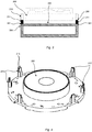
Fig. 4 is a perspective view of a chuck according to one embodiment of the present invention; -
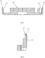
Fig. 5 is a cross sectional view of a chuck according to one embodiment of the present invention; and -
Fig. 6 is a cross sectional view of a lateral part of a chuck according to one embodiment of the present invention. - The following description focuses on embodiments of the present invention applicable to a method for leveling a master electrode and a substrate during ECPR. However, it will be appreciated that the invention is not limited to this application but may be applied to many other replication, patterning or bonding processes within the field of micro electronics and/or mechanics where leveling of two surfaces is beneficial, including for example wafer bonding, various lithographic processes, dry or wet etching processes, etc.
- In
Fig. 1 a schematic view of an ECPR setting is disclosed. A lower and anupper chuck master electrode 103 and asubstrate 104, respectively. Themaster electrode 103 comprises a conducting disc, at least one insulating layer arranged on the conducting disc, cavities in the insulating layer and/or in the conducting disc, a substantially inert electrode layer arranged in the bottom of said cavities on the conducting disc and may comprise an anode material (such as copper), dissolvable in an electrochemical process, arranged in said cavities on the electrode layer. An electrolyte is provided between themaster electrode 103 and thesubstrate 104, such that electrochemical cells are created between the two, defined by the (patterned) insulating material (not shown), electrode layer (not shown) or prefilled anode material (not shown) on themaster electrode 103 and the substrate. Due to the fact that themaster electrode 103 and thesubstrate 104 are to be in close contact, in such a manner that the insulating material of themaster electrode 103 closes the electrochemical cells in all positions of the interaction, it is important that themaster electrode 103 and thesubstrate 104, and thus the lower andupper chucks -
Fig. 2 discloses anupper chuck 200 according an embodiment of the present invention. For the sake of convenience, only embodiments relating to the upper chuck will be described below, although the same arrangements are equally possible for the lower chuck. Theupper chuck 200 has a proximal end a distal end. Theupper chuck 200 is hanging from a semi-sphere-socket bearing. In the proximal end theupper chuck 200 may comprise asemi-spherical head 201. The semi-spherical head 201 is positioned in acavity 202 in anupper chamber piece 203. Theupper chamber piece 203 comprises a central concavesemi-spherical surface 204, having a radius corresponding to the radius of thesemi-spherical head 201, such that thehead 201 may rotate in saidconcave surface 204 in a ball in joint manner. Thehead 201 may be spring mounted to theupper chamber piece 203, such that thehead 201 is locked in position during a first pressure in thecavity 202. The pre-loading force between the two surfaces, acting to lock them in position, can be further increased by arranging vacuum or reduced pressure in portions of the surfaces between thespherical head 201 and theupper chamber piece 203. When applying a pressure in thecavity 202 being higher than the first pressure, thehead 201 is released, and will float against theconcave surface 204. In this way theupper chuck 200 and aninteraction surface 205, for holding asubstrate 206 or a master electrode, will float in three dimensions, having a rotational centre in acentre point 207, the rotational centre being determined by the radius of the semi-spherical surfaces of the semi- spherical head. Thesubstrate 206 or the master electrode may be held to the interaction surface by suitable holding means, such as applied vacuum in a sealed of area between thechuck 200 and the substrate or master electrode, or other mechanical holding means, such as circumferentially arranged clamps etc. Thecentre point 207 may preferably be positioned in the centre of theinteraction surface 205. Theinteraction surface 205 has a under the circumstances planar configuration. This means that the proximodistal variation when theinteraction surface 205 is horizontally aligned is below 3 micrometers. Then theinteraction surface 205 will float while keeping thiscentre point 207 in the same vertical and horizontal position. Laterally of the head 201 a second convex segmental-spherical surface 208 on theupper chuck 200 may interact in the same manner with a concave segmental-spherical surface 209, the segmental-spherical surfaces having a radius r2 such that their point of rotation also will be positioned in thecentre point 207. In this way a more steady bearing may be obtained, assuring minimized lateral movement and minimized movement of the centre point of theinteraction surface 205. - Other arrangements than floating ball in socket arrangements are equally possible, such as loosening a chuck stem (not shown) from a tightening arrangement in an upper piece allowing for plane alignment, and then tighten the tightening arrangement, once the leveling has been performed. It is however preferable to use the floating ball in socket arrangement according to above, since this allows for quick and reliable leveling, which is of special importance in the quest for improved manufacturing methods of printed wafers, to satisfy the high demand from the society.
- Laterally of the
interaction surface 205 levelingteeth 210 are arranged. By arranging the levelingteeth 210 laterally of theinteraction surface 205, creates a long lever for rotational movement to make sure the parallelism between the two chucks can be established without undue force. Also the margin of error may be decreased. The levelingteeth 210 are evenly distributed circumferentially of theinteraction surface 205. The levelingteeth 210 may for example be distributed circumferentially of the interaction surface with 120 degrees apart, calculated from the centre axis. To ensure that the levelingteeth 210 will define a plane between their distal end points, at least three levelingteeth 210 are arranged circumferentially of theinteraction surface 205. The levelingteeth 210 extend distally beyond theinteraction surface 205 when theinteraction surface 205 is in the horizontal plane. The distal end points of the levelingteeth 210 define a plane that is parallel and distally positioned with regard to the plane of theinteraction surface 205. The difference in distal position between the plane of theinteraction surface 205 and the plane defined by the levelingteeth 210 may be just smaller than the sum of the thickness of the master electrode and the thickness of the substrate. In this way, leveling can be performed without master electrode and substrate in place on the lower and upper chuck pieces, respectively, while subsequently performing printing with leveled chucks without having to remove the leveling teeth. - In
Fig. 3 it is disclosed how anupper chuck 200 of this kind has been brought into contact with alower chuck 300, such that the levelingteeth 210 are sitting on aleveling area 301 on thelower chuck 300. The levelingarea 301 is positioned circumferentially of aninteraction surface 302 for holding a master electrode. The levelingarea 301 and theinteraction surface 302 are parallel and may be located in the same plane for ease of manufacture, due to facilitated one step polishing step of both theleveling area 301 and theinteraction surface 302, and to simplify later electrolyte injection etc. The levelingarea 301 has full mechanical support beneath the surface of the levelingarea 301, such that the leveling area becomes rigid. - When performing the leveling, the
upper chuck 200 is loosened from theupper chamber piece 203, by applying a suitable pressure in thecavity 202, such that the upper chuck starts to float, and the plane of theinteraction surface 205 and the levelingteeth 210 becomes adjustable in space. Then theupper chuck 200 is lowered into contact with thelower chuck 300 and the levelingteeth 210 will sit on aleveling area 301, such as disclosed inFig. 3 . When the levelingteeth 210 sits on the levelingarea 301 theinteraction surface 205 and theinteraction surface 302 will be parallel. In this position theupper chuck 200 is locked to theupper chamber piece 203 by releasing the pressure in thecavity 202. - The leveling
teeth 210 may comprisedistance members 211, as disclosed inFig. 3 . When the levelingteeth 210 comprisedistance members 211, leveling teeth base 212 may be manufactured by polishing at the same time as the interaction asurface 205, as disclosed inFigs. 4 to 6 . Thereafter holes 213 for receiving thedistance members 211 are accurately drilled into theteeth base 212, as disclosed inFigs. 4 . and6 . Thedistance members 211 are then manufactured with the same height, such that they will provide the same distal extension from theteeth base 212. Thus it can be assured that the distal end points of the levelingteeth 210, in this embodiment the distal end points of thedistance members 211, define a plane that is parallel with theinteraction surface 205. Thedistance members 211 may be manufactured in a magnetic material. When thedistance members 211 are manufactured in a magnetic material, there is no need for adding additional material, such as glue or other adhesive, which would make it difficult to control that the plane defined by the distal end points of the levelingteeth 210 and the plane of theinteraction surface 205 are parallel. Also, such distance members may be securely used in upper chucks without falling out of theholes 213 in theteeth base 212. - It is readily understood that all references to lower/upper are merely for illustrative purposes, without any limiting effect on the scope of protection. Moreover, it should be realized that equivalent setups to those described may include setups having a substrate arranged on a lower chuck while the master electrode is mounted on an upper chuck, as well as setups in which the positions of the lower and upper chuck are switched.
Claims (14)
- A chuck for holding a substrate or master electrode in an electrochemical pattern replication (ECPR) process, said chuck having a proximal and a distal end, said chuck comprising
an interaction surface (205) for holding the substrate or master electrode positioned in a first plane;
holding means for holding the substrate or master electrode to said interaction surface (205);
leveling teeth (210) arranged laterally and circumferentially of said interaction surface and extending distally beyond the interaction surface (205), the distal end points of said leveling teeth (210) defining a second plane;
wherein said second plane is parallel to the first plane and positioned distally of the first plane. - The chuck according to claim 1, wherein the leveling teeth (210) are evenly distributed around the interaction surface (205).
- The chuck according to claim 1 or 2, wherein the leveling teeth (210) are distributed circumferentially of the interaction surface with 120 degrees apart, calculated from a centre axis of the chuck.
- The chuck according to any of the preceding claims, wherein the number of leveling teeth (210) is at least three.
- The chuck according to any of the preceding claims, wherein said leveling teeth (210) comprise teeth bases (212), respectively, said teeth bases (212) being positioned in the first plane, and distance members (211) extending distally from said teeth bases (212), such that the distal end points of the leveling teeth are the distal end points of the distance members (211).
- The chuck according to claim 5, wherein the distance members (211) are inserted in holes (213) in the teeth bases (212).
- The chuck according to claim 5 or 6, wherein the distance members are magnetic.
- The chuck according to any of the preceding claims, wherein the proximal end of the chuck comprises a semi-spherical head (201), said semi-spherical head (201) being positioned in a cavity (202) in a chamber piece (203), said chamber piece (203) comprising a concave semi-spherical surface (204), having a first radius (r1) corresponding to the radius of the semi-spherical head (201), such that the semi-spherical head (201) may rotate in said concave surface (204) in a ball in joint manner, there being provided a gas inlet to said cavity (202).
- The chuck according to claim 8, wherein the semi- spherical head (201) is spring mounted to the chamber piece (203).
- The chuck according to claim 9, wherein the semi-spherical head (201) is spring mounted and portions of the surface pre-loaded with vacuum to the chamber piece (203).
- The chuck according to claim 8 or 10, comprising a second convex segmental-spherical surface (208) interact with a concave segmental-spherical surface (209) on the chamber piece (203), said segmental-spherical surfaces having a second radius (r2).
- The chuck according to any of claims 8 to 11, wherein the first radius (r1) and the second radius (r2) have the same rotational centre positioned in a centre point (207) on the interaction surface (205).
- A chuck assembly, comprising a chuck according to any of claims 1 to 12, and an opposite chuck, said opposite chuck comprising an interaction surface (302) for holding the substrate or master electrode positioned in a third plane; holding means for holding the substrate or master electrode to said interaction surface (302); a rigid leveling area (301) laterally and circumferentially of said interaction surface (302), said leveling area (301) corresponding in lateral position to the lateral position of the leveling teeth (210), said leveling area (301) and interaction surface (302) being parallel.
- A method of leveling a chuck assembly according to claim 13, comprising loosening the chuck according to any of claims 1 to 11,
bringing the chuck according to any of claims 1 to 11 and the opposite chuck into contact, such that the leveling teeth (210) will sit on the leveling area (301),
locking the chuck according to any of claims 1 to 11, such that the plane of the interaction surface (205) of the chuck according to any of claims 1 to 11 is fixated to be parallel to the plane of the interaction surface (302).
Applications Claiming Priority (3)
| Application Number | Priority Date | Filing Date | Title |
|---|---|---|---|
| SE1050799 | 2010-07-15 | ||
| US36498910P | 2010-07-16 | 2010-07-16 | |
| PCT/EP2011/061993 WO2012007523A1 (en) | 2010-07-15 | 2011-07-13 | Leveling of master electrode and substrate in ecpr, and a chuck therefor |
Publications (2)
| Publication Number | Publication Date |
|---|---|
| EP2593585A1 EP2593585A1 (en) | 2013-05-22 |
| EP2593585B1 true EP2593585B1 (en) | 2017-08-30 |
Family
ID=44630429
Family Applications (1)
| Application Number | Title | Priority Date | Filing Date |
|---|---|---|---|
| EP11745503.0A Not-in-force EP2593585B1 (en) | 2010-07-15 | 2011-07-13 | Leveling of master electrode and substrate in ecpr, and a chuck therefor |
Country Status (3)
| Country | Link |
|---|---|
| EP (1) | EP2593585B1 (en) |
| ES (1) | ES2650449T3 (en) |
| WO (1) | WO2012007523A1 (en) |
Family Cites Families (3)
| Publication number | Priority date | Publication date | Assignee | Title |
|---|---|---|---|---|
| JPS5988831A (en) * | 1982-11-12 | 1984-05-22 | Toshiba Corp | Manufacture of semiconductor device |
| SE523309E (en) | 2001-06-15 | 2010-03-02 | Replisaurus Technologies Ab | Method, electrode and apparatus for creating micro- and nanostructures in conductive materials by patterning with master electrode and electrolyte |
| JP3974843B2 (en) * | 2002-11-15 | 2007-09-12 | 株式会社アルテクス | Ultrasonic bonding equipment |
-
2011
- 2011-07-13 ES ES11745503.0T patent/ES2650449T3/en active Active
- 2011-07-13 EP EP11745503.0A patent/EP2593585B1/en not_active Not-in-force
- 2011-07-13 WO PCT/EP2011/061993 patent/WO2012007523A1/en not_active Ceased
Non-Patent Citations (1)
| Title |
|---|
| None * |
Also Published As
| Publication number | Publication date |
|---|---|
| EP2593585A1 (en) | 2013-05-22 |
| WO2012007523A1 (en) | 2012-01-19 |
| ES2650449T3 (en) | 2018-01-18 |
Similar Documents
| Publication | Publication Date | Title |
|---|---|---|
| TWI891615B (en) | Low temperature direct copper-copper bonding | |
| CN101360850B (en) | Main electrode and its forming method | |
| US8556389B2 (en) | Low-profile MEMS thermal printhead die having backside electrical connections | |
| TWI639215B (en) | Substrate with protruding copper terminal posts | |
| KR20120031140A (en) | Interposer with microspring contacts and methods of making and using same | |
| CN101770963B (en) | Method of forming conductive layer and semiconductor device | |
| EP2593586B1 (en) | A chuck, and a method for bringing a first and a second substrate together | |
| Lin et al. | High density and through wafer copper interconnections and solder bumps for MEMS wafer-level packaging | |
| EP2593585A1 (en) | Leveling of master electrode and substrate in ecpr, and a chuck therefor | |
| WO2011123717A1 (en) | Interconnect structures and methods of making the same | |
| ITMI20060478A1 (en) | SYSTEM FOR CONTACTING ELECTRONIC DEVICES AND ITS PRODUCTION METHOD BASED ON WIRED CONDUCTOR IN INSULATING MATERIAL | |
| EP2593584B1 (en) | Device, system and method for use in machines for electrochemical pattern replication | |
| US7563703B2 (en) | Microelectronic interconnect device comprising localised conductive pins | |
| KR101381632B1 (en) | Apparatus to plate substrate | |
| CN118633172A (en) | Method for manufacturing semiconductor device and semiconductor device | |
| EP2593592B1 (en) | Separation of master electrode and substrate in ecpr | |
| EP2593588B1 (en) | A contact sheet for arrangement between a chuck and a master electrode in an ecpr process | |
| Chan et al. | Low cost, high density interposers in aluminum oxide films | |
| US12104266B2 (en) | Plating apparatus having conductive liquid and plating method | |
| Naik et al. | Electrochemical deposition and characterization of Copper Pillar Bumps—Application towards Flip chip bonding | |
| JP6223421B2 (en) | Method of temporarily bonding a chip having a contact element to a substrate having a functional layer having an opening for the chip contact element | |
| Tian et al. | High density indium bumping through pulse plating used for pixel X-ray detectors | |
| KR20260011841A (en) | Jig for double-sided plating and device of filling conductive metal in through hole of substrate including the same | |
| TW202539016A (en) | Anisotropic conductive component and joint | |
| CN120784244A (en) | Semiconductor testing device and method for manufacturing the same |
Legal Events
| Date | Code | Title | Description |
|---|---|---|---|
| PUAI | Public reference made under article 153(3) epc to a published international application that has entered the european phase |
Free format text: ORIGINAL CODE: 0009012 |
|
| 17P | Request for examination filed |
Effective date: 20130130 |
|
| AK | Designated contracting states |
Kind code of ref document: A1 Designated state(s): AL AT BE BG CH CY CZ DE DK EE ES FI FR GB GR HR HU IE IS IT LI LT LU LV MC MK MT NL NO PL PT RO RS SE SI SK SM TR |
|
| DAX | Request for extension of the european patent (deleted) | ||
| 17Q | First examination report despatched |
Effective date: 20160225 |
|
| GRAP | Despatch of communication of intention to grant a patent |
Free format text: ORIGINAL CODE: EPIDOSNIGR1 |
|
| STAA | Information on the status of an ep patent application or granted ep patent |
Free format text: STATUS: GRANT OF PATENT IS INTENDED |
|
| INTG | Intention to grant announced |
Effective date: 20170221 |
|
| GRAS | Grant fee paid |
Free format text: ORIGINAL CODE: EPIDOSNIGR3 |
|
| GRAA | (expected) grant |
Free format text: ORIGINAL CODE: 0009210 |
|
| STAA | Information on the status of an ep patent application or granted ep patent |
Free format text: STATUS: THE PATENT HAS BEEN GRANTED |
|
| RAP1 | Party data changed (applicant data changed or rights of an application transferred) |
Owner name: LUXEMBOURG INSTITUTE OF SCIENCE AND TECHNOLOGY (LI |
|
| AK | Designated contracting states |
Kind code of ref document: B1 Designated state(s): AL AT BE BG CH CY CZ DE DK EE ES FI FR GB GR HR HU IE IS IT LI LT LU LV MC MK MT NL NO PL PT RO RS SE SI SK SM TR |
|
| REG | Reference to a national code |
Ref country code: GB Ref legal event code: FG4D |
|
| REG | Reference to a national code |
Ref country code: CH Ref legal event code: EP |
|
| REG | Reference to a national code |
Ref country code: AT Ref legal event code: REF Ref document number: 923650 Country of ref document: AT Kind code of ref document: T Effective date: 20170915 |
|
| REG | Reference to a national code |
Ref country code: IE Ref legal event code: FG4D |
|
| REG | Reference to a national code |
Ref country code: DE Ref legal event code: R096 Ref document number: 602011041082 Country of ref document: DE |
|
| REG | Reference to a national code |
Ref country code: CH Ref legal event code: NV Representative=s name: DR. ALEXANDER MILLER, LL.M. RECHTSANWALT (D), CH |
|
| REG | Reference to a national code |
Ref country code: NL Ref legal event code: FP |
|
| REG | Reference to a national code |
Ref country code: SE Ref legal event code: TRGR |
|
| REG | Reference to a national code |
Ref country code: LT Ref legal event code: MG4D |
|
| REG | Reference to a national code |
Ref country code: ES Ref legal event code: FG2A Ref document number: 2650449 Country of ref document: ES Kind code of ref document: T3 Effective date: 20180118 |
|
| PG25 | Lapsed in a contracting state [announced via postgrant information from national office to epo] |
Ref country code: LT Free format text: LAPSE BECAUSE OF FAILURE TO SUBMIT A TRANSLATION OF THE DESCRIPTION OR TO PAY THE FEE WITHIN THE PRESCRIBED TIME-LIMIT Effective date: 20170830 Ref country code: HR Free format text: LAPSE BECAUSE OF FAILURE TO SUBMIT A TRANSLATION OF THE DESCRIPTION OR TO PAY THE FEE WITHIN THE PRESCRIBED TIME-LIMIT Effective date: 20170830 Ref country code: NO Free format text: LAPSE BECAUSE OF FAILURE TO SUBMIT A TRANSLATION OF THE DESCRIPTION OR TO PAY THE FEE WITHIN THE PRESCRIBED TIME-LIMIT Effective date: 20171130 |
|
| PG25 | Lapsed in a contracting state [announced via postgrant information from national office to epo] |
Ref country code: LV Free format text: LAPSE BECAUSE OF FAILURE TO SUBMIT A TRANSLATION OF THE DESCRIPTION OR TO PAY THE FEE WITHIN THE PRESCRIBED TIME-LIMIT Effective date: 20170830 Ref country code: RS Free format text: LAPSE BECAUSE OF FAILURE TO SUBMIT A TRANSLATION OF THE DESCRIPTION OR TO PAY THE FEE WITHIN THE PRESCRIBED TIME-LIMIT Effective date: 20170830 Ref country code: BG Free format text: LAPSE BECAUSE OF FAILURE TO SUBMIT A TRANSLATION OF THE DESCRIPTION OR TO PAY THE FEE WITHIN THE PRESCRIBED TIME-LIMIT Effective date: 20171130 Ref country code: IS Free format text: LAPSE BECAUSE OF FAILURE TO SUBMIT A TRANSLATION OF THE DESCRIPTION OR TO PAY THE FEE WITHIN THE PRESCRIBED TIME-LIMIT Effective date: 20171230 Ref country code: GR Free format text: LAPSE BECAUSE OF FAILURE TO SUBMIT A TRANSLATION OF THE DESCRIPTION OR TO PAY THE FEE WITHIN THE PRESCRIBED TIME-LIMIT Effective date: 20171201 |
|
| PG25 | Lapsed in a contracting state [announced via postgrant information from national office to epo] |
Ref country code: DK Free format text: LAPSE BECAUSE OF FAILURE TO SUBMIT A TRANSLATION OF THE DESCRIPTION OR TO PAY THE FEE WITHIN THE PRESCRIBED TIME-LIMIT Effective date: 20170830 Ref country code: RO Free format text: LAPSE BECAUSE OF FAILURE TO SUBMIT A TRANSLATION OF THE DESCRIPTION OR TO PAY THE FEE WITHIN THE PRESCRIBED TIME-LIMIT Effective date: 20170830 Ref country code: PL Free format text: LAPSE BECAUSE OF FAILURE TO SUBMIT A TRANSLATION OF THE DESCRIPTION OR TO PAY THE FEE WITHIN THE PRESCRIBED TIME-LIMIT Effective date: 20170830 Ref country code: CZ Free format text: LAPSE BECAUSE OF FAILURE TO SUBMIT A TRANSLATION OF THE DESCRIPTION OR TO PAY THE FEE WITHIN THE PRESCRIBED TIME-LIMIT Effective date: 20170830 |
|
| PG25 | Lapsed in a contracting state [announced via postgrant information from national office to epo] |
Ref country code: SM Free format text: LAPSE BECAUSE OF FAILURE TO SUBMIT A TRANSLATION OF THE DESCRIPTION OR TO PAY THE FEE WITHIN THE PRESCRIBED TIME-LIMIT Effective date: 20170830 Ref country code: SK Free format text: LAPSE BECAUSE OF FAILURE TO SUBMIT A TRANSLATION OF THE DESCRIPTION OR TO PAY THE FEE WITHIN THE PRESCRIBED TIME-LIMIT Effective date: 20170830 Ref country code: IT Free format text: LAPSE BECAUSE OF FAILURE TO SUBMIT A TRANSLATION OF THE DESCRIPTION OR TO PAY THE FEE WITHIN THE PRESCRIBED TIME-LIMIT Effective date: 20170830 Ref country code: EE Free format text: LAPSE BECAUSE OF FAILURE TO SUBMIT A TRANSLATION OF THE DESCRIPTION OR TO PAY THE FEE WITHIN THE PRESCRIBED TIME-LIMIT Effective date: 20170830 |
|
| REG | Reference to a national code |
Ref country code: DE Ref legal event code: R097 Ref document number: 602011041082 Country of ref document: DE |
|
| PLBE | No opposition filed within time limit |
Free format text: ORIGINAL CODE: 0009261 |
|
| STAA | Information on the status of an ep patent application or granted ep patent |
Free format text: STATUS: NO OPPOSITION FILED WITHIN TIME LIMIT |
|
| REG | Reference to a national code |
Ref country code: FR Ref legal event code: PLFP Year of fee payment: 8 |
|
| 26N | No opposition filed |
Effective date: 20180531 |
|
| PG25 | Lapsed in a contracting state [announced via postgrant information from national office to epo] |
Ref country code: SI Free format text: LAPSE BECAUSE OF FAILURE TO SUBMIT A TRANSLATION OF THE DESCRIPTION OR TO PAY THE FEE WITHIN THE PRESCRIBED TIME-LIMIT Effective date: 20170830 |
|
| PG25 | Lapsed in a contracting state [announced via postgrant information from national office to epo] |
Ref country code: MC Free format text: LAPSE BECAUSE OF FAILURE TO SUBMIT A TRANSLATION OF THE DESCRIPTION OR TO PAY THE FEE WITHIN THE PRESCRIBED TIME-LIMIT Effective date: 20170830 |
|
| REG | Reference to a national code |
Ref country code: BE Ref legal event code: MM Effective date: 20180731 |
|
| REG | Reference to a national code |
Ref country code: IE Ref legal event code: MM4A |
|
| PG25 | Lapsed in a contracting state [announced via postgrant information from national office to epo] |
Ref country code: IE Free format text: LAPSE BECAUSE OF NON-PAYMENT OF DUE FEES Effective date: 20180713 |
|
| PG25 | Lapsed in a contracting state [announced via postgrant information from national office to epo] |
Ref country code: BE Free format text: LAPSE BECAUSE OF NON-PAYMENT OF DUE FEES Effective date: 20180731 |
|
| PGFP | Annual fee paid to national office [announced via postgrant information from national office to epo] |
Ref country code: NL Payment date: 20190719 Year of fee payment: 9 Ref country code: LU Payment date: 20190723 Year of fee payment: 9 |
|
| PGFP | Annual fee paid to national office [announced via postgrant information from national office to epo] |
Ref country code: FR Payment date: 20190723 Year of fee payment: 9 Ref country code: FI Payment date: 20190722 Year of fee payment: 9 Ref country code: SE Payment date: 20190723 Year of fee payment: 9 Ref country code: ES Payment date: 20190807 Year of fee payment: 9 Ref country code: DE Payment date: 20190723 Year of fee payment: 9 |
|
| PGFP | Annual fee paid to national office [announced via postgrant information from national office to epo] |
Ref country code: GB Payment date: 20190718 Year of fee payment: 9 Ref country code: AT Payment date: 20190718 Year of fee payment: 9 |
|
| PG25 | Lapsed in a contracting state [announced via postgrant information from national office to epo] |
Ref country code: MT Free format text: LAPSE BECAUSE OF NON-PAYMENT OF DUE FEES Effective date: 20180713 |
|
| PGFP | Annual fee paid to national office [announced via postgrant information from national office to epo] |
Ref country code: CH Payment date: 20190729 Year of fee payment: 9 |
|
| PG25 | Lapsed in a contracting state [announced via postgrant information from national office to epo] |
Ref country code: TR Free format text: LAPSE BECAUSE OF FAILURE TO SUBMIT A TRANSLATION OF THE DESCRIPTION OR TO PAY THE FEE WITHIN THE PRESCRIBED TIME-LIMIT Effective date: 20170830 |
|
| REG | Reference to a national code |
Ref country code: AT Ref legal event code: UEP Ref document number: 923650 Country of ref document: AT Kind code of ref document: T Effective date: 20170830 |
|
| PG25 | Lapsed in a contracting state [announced via postgrant information from national office to epo] |
Ref country code: PT Free format text: LAPSE BECAUSE OF FAILURE TO SUBMIT A TRANSLATION OF THE DESCRIPTION OR TO PAY THE FEE WITHIN THE PRESCRIBED TIME-LIMIT Effective date: 20170830 Ref country code: HU Free format text: LAPSE BECAUSE OF FAILURE TO SUBMIT A TRANSLATION OF THE DESCRIPTION OR TO PAY THE FEE WITHIN THE PRESCRIBED TIME-LIMIT; INVALID AB INITIO Effective date: 20110713 |
|
| PG25 | Lapsed in a contracting state [announced via postgrant information from national office to epo] |
Ref country code: CY Free format text: LAPSE BECAUSE OF FAILURE TO SUBMIT A TRANSLATION OF THE DESCRIPTION OR TO PAY THE FEE WITHIN THE PRESCRIBED TIME-LIMIT Effective date: 20170830 Ref country code: MK Free format text: LAPSE BECAUSE OF NON-PAYMENT OF DUE FEES Effective date: 20170830 |
|
| PG25 | Lapsed in a contracting state [announced via postgrant information from national office to epo] |
Ref country code: AL Free format text: LAPSE BECAUSE OF FAILURE TO SUBMIT A TRANSLATION OF THE DESCRIPTION OR TO PAY THE FEE WITHIN THE PRESCRIBED TIME-LIMIT Effective date: 20170830 |
|
| REG | Reference to a national code |
Ref country code: DE Ref legal event code: R119 Ref document number: 602011041082 Country of ref document: DE |
|
| REG | Reference to a national code |
Ref country code: FI Ref legal event code: MAE |
|
| REG | Reference to a national code |
Ref country code: CH Ref legal event code: PL |
|
| REG | Reference to a national code |
Ref country code: SE Ref legal event code: EUG |
|
| REG | Reference to a national code |
Ref country code: NL Ref legal event code: MM Effective date: 20200801 |
|
| REG | Reference to a national code |
Ref country code: AT Ref legal event code: MM01 Ref document number: 923650 Country of ref document: AT Kind code of ref document: T Effective date: 20200713 |
|
| GBPC | Gb: european patent ceased through non-payment of renewal fee |
Effective date: 20200713 |
|
| PG25 | Lapsed in a contracting state [announced via postgrant information from national office to epo] |
Ref country code: LI Free format text: LAPSE BECAUSE OF NON-PAYMENT OF DUE FEES Effective date: 20200731 Ref country code: CH Free format text: LAPSE BECAUSE OF NON-PAYMENT OF DUE FEES Effective date: 20200731 Ref country code: NL Free format text: LAPSE BECAUSE OF NON-PAYMENT OF DUE FEES Effective date: 20200801 Ref country code: LU Free format text: LAPSE BECAUSE OF NON-PAYMENT OF DUE FEES Effective date: 20200713 Ref country code: GB Free format text: LAPSE BECAUSE OF NON-PAYMENT OF DUE FEES Effective date: 20200713 Ref country code: FI Free format text: LAPSE BECAUSE OF NON-PAYMENT OF DUE FEES Effective date: 20200713 Ref country code: FR Free format text: LAPSE BECAUSE OF NON-PAYMENT OF DUE FEES Effective date: 20200731 |
|
| PG25 | Lapsed in a contracting state [announced via postgrant information from national office to epo] |
Ref country code: SE Free format text: LAPSE BECAUSE OF NON-PAYMENT OF DUE FEES Effective date: 20200714 Ref country code: DE Free format text: LAPSE BECAUSE OF NON-PAYMENT OF DUE FEES Effective date: 20210202 Ref country code: AT Free format text: LAPSE BECAUSE OF NON-PAYMENT OF DUE FEES Effective date: 20200713 |
|
| REG | Reference to a national code |
Ref country code: ES Ref legal event code: FD2A Effective date: 20211228 |
|
| PG25 | Lapsed in a contracting state [announced via postgrant information from national office to epo] |
Ref country code: ES Free format text: LAPSE BECAUSE OF NON-PAYMENT OF DUE FEES Effective date: 20200714 |