EP2592907A1 - A circuit for driving light sources, relative lighting system and method of driving light sources - Google Patents
A circuit for driving light sources, relative lighting system and method of driving light sources Download PDFInfo
- Publication number
- EP2592907A1 EP2592907A1 EP20120188088 EP12188088A EP2592907A1 EP 2592907 A1 EP2592907 A1 EP 2592907A1 EP 20120188088 EP20120188088 EP 20120188088 EP 12188088 A EP12188088 A EP 12188088A EP 2592907 A1 EP2592907 A1 EP 2592907A1
- Authority
- EP
- European Patent Office
- Prior art keywords
- light source
- switching means
- light sources
- inductive element
- series
- Prior art date
- Legal status (The legal status is an assumption and is not a legal conclusion. Google has not performed a legal analysis and makes no representation as to the accuracy of the status listed.)
- Granted
Links
- 238000000034 method Methods 0.000 title claims description 5
- 230000001939 inductive effect Effects 0.000 claims abstract description 29
- 238000004519 manufacturing process Methods 0.000 description 2
- 239000000463 material Substances 0.000 description 2
- 230000003287 optical effect Effects 0.000 description 2
- 230000010355 oscillation Effects 0.000 description 2
- 238000010586 diagram Methods 0.000 description 1
- 230000005669 field effect Effects 0.000 description 1
- 239000004065 semiconductor Substances 0.000 description 1
- 230000001360 synchronised effect Effects 0.000 description 1
Images



Classifications
-
- H—ELECTRICITY
- H05—ELECTRIC TECHNIQUES NOT OTHERWISE PROVIDED FOR
- H05B—ELECTRIC HEATING; ELECTRIC LIGHT SOURCES NOT OTHERWISE PROVIDED FOR; CIRCUIT ARRANGEMENTS FOR ELECTRIC LIGHT SOURCES, IN GENERAL
- H05B45/00—Circuit arrangements for operating light-emitting diodes [LED]
- H05B45/30—Driver circuits
- H05B45/37—Converter circuits
- H05B45/3725—Switched mode power supply [SMPS]
- H05B45/39—Circuits containing inverter bridges
-
- H—ELECTRICITY
- H05—ELECTRIC TECHNIQUES NOT OTHERWISE PROVIDED FOR
- H05B—ELECTRIC HEATING; ELECTRIC LIGHT SOURCES NOT OTHERWISE PROVIDED FOR; CIRCUIT ARRANGEMENTS FOR ELECTRIC LIGHT SOURCES, IN GENERAL
- H05B45/00—Circuit arrangements for operating light-emitting diodes [LED]
- H05B45/30—Driver circuits
- H05B45/37—Converter circuits
-
- H—ELECTRICITY
- H05—ELECTRIC TECHNIQUES NOT OTHERWISE PROVIDED FOR
- H05B—ELECTRIC HEATING; ELECTRIC LIGHT SOURCES NOT OTHERWISE PROVIDED FOR; CIRCUIT ARRANGEMENTS FOR ELECTRIC LIGHT SOURCES, IN GENERAL
- H05B45/00—Circuit arrangements for operating light-emitting diodes [LED]
- H05B45/10—Controlling the intensity of the light
-
- H—ELECTRICITY
- H05—ELECTRIC TECHNIQUES NOT OTHERWISE PROVIDED FOR
- H05B—ELECTRIC HEATING; ELECTRIC LIGHT SOURCES NOT OTHERWISE PROVIDED FOR; CIRCUIT ARRANGEMENTS FOR ELECTRIC LIGHT SOURCES, IN GENERAL
- H05B45/00—Circuit arrangements for operating light-emitting diodes [LED]
- H05B45/40—Details of LED load circuits
- H05B45/44—Details of LED load circuits with an active control inside an LED matrix
-
- H—ELECTRICITY
- H05—ELECTRIC TECHNIQUES NOT OTHERWISE PROVIDED FOR
- H05B—ELECTRIC HEATING; ELECTRIC LIGHT SOURCES NOT OTHERWISE PROVIDED FOR; CIRCUIT ARRANGEMENTS FOR ELECTRIC LIGHT SOURCES, IN GENERAL
- H05B45/00—Circuit arrangements for operating light-emitting diodes [LED]
- H05B45/40—Details of LED load circuits
- H05B45/44—Details of LED load circuits with an active control inside an LED matrix
- H05B45/46—Details of LED load circuits with an active control inside an LED matrix having LEDs disposed in parallel lines
-
- H—ELECTRICITY
- H05—ELECTRIC TECHNIQUES NOT OTHERWISE PROVIDED FOR
- H05B—ELECTRIC HEATING; ELECTRIC LIGHT SOURCES NOT OTHERWISE PROVIDED FOR; CIRCUIT ARRANGEMENTS FOR ELECTRIC LIGHT SOURCES, IN GENERAL
- H05B45/00—Circuit arrangements for operating light-emitting diodes [LED]
- H05B45/40—Details of LED load circuits
- H05B45/44—Details of LED load circuits with an active control inside an LED matrix
- H05B45/48—Details of LED load circuits with an active control inside an LED matrix having LEDs organised in strings and incorporating parallel shunting devices
-
- H—ELECTRICITY
- H05—ELECTRIC TECHNIQUES NOT OTHERWISE PROVIDED FOR
- H05B—ELECTRIC HEATING; ELECTRIC LIGHT SOURCES NOT OTHERWISE PROVIDED FOR; CIRCUIT ARRANGEMENTS FOR ELECTRIC LIGHT SOURCES, IN GENERAL
- H05B47/00—Circuit arrangements for operating light sources in general, i.e. where the type of light source is not relevant
- H05B47/10—Controlling the light source
-
- Y—GENERAL TAGGING OF NEW TECHNOLOGICAL DEVELOPMENTS; GENERAL TAGGING OF CROSS-SECTIONAL TECHNOLOGIES SPANNING OVER SEVERAL SECTIONS OF THE IPC; TECHNICAL SUBJECTS COVERED BY FORMER USPC CROSS-REFERENCE ART COLLECTIONS [XRACs] AND DIGESTS
- Y02—TECHNOLOGIES OR APPLICATIONS FOR MITIGATION OR ADAPTATION AGAINST CLIMATE CHANGE
- Y02B—CLIMATE CHANGE MITIGATION TECHNOLOGIES RELATED TO BUILDINGS, e.g. HOUSING, HOUSE APPLIANCES OR RELATED END-USER APPLICATIONS
- Y02B20/00—Energy efficient lighting technologies, e.g. halogen lamps or gas discharge lamps
- Y02B20/30—Semiconductor lamps, e.g. solid state lamps [SSL] light emitting diodes [LED] or organic LED [OLED]
Definitions
- the present disclosure relates to circuits for driving light sources.
- Electronic converters for light sources comprising, for example, at least one LED (Light Emitting Diode) usually supply an output direct current.
- a current may be stable or vary in time, for example, in order to regulate the intensity of the light emitted by the light source (so called "dimming" function).
- Figure 1 shows a possible lighting system comprising an electronic converter 10 and a LED module 20, including at least one LED L.
- Electronic converter 10 usually comprises a control circuit 102 (for example a microprocessor) and a power circuit 104 (for example a switching power supply AC/DC or DC/DC) receiving as input a supply signal (for example from the electric line) and outputting, through a power output 106, a direct current.
- This current may be stable or can vary in time.
- control circuit 102 may set, via a reference channel I Ref of power circuit 104, the current required by LED module 20.
- LED module 20 may also comprise an identification element, which identifies the current required by LED module 20 (or in general control parameters).
- control circuit 102 communicates with the identification element, and adjusts the operation of the electronic converter to the operating conditions required by the LED module.
- Figure 1 also shows two switches 108 and 110.
- the first switch 108 permits to regulate the light intensity emitted by LED module 20.
- switch 108 may be driven via a pulse-width modulation (PWM) in order to selectively short-circuit LED module 20, while deviating the current from generator 104 onto switch 108.
- PWM pulse-width modulation
- a brightness regulation of the light intensity emitted by LED module 20 can also be achieved by setting a lower reference current I Ref .
- the second switch 110 allows to deactivate the supply to LED module 20.
- an electronic converter may deactivate the supply when an error condition is detected, or for reasons of reliability, for example when an over-current, over-voltage or over-temperature condition is detected.
- LED module 20 may comprise one single LED or a LED chain or string, wherein a plurality of LEDs are connected in series.
- IEC International Electrotechnical Commission
- UL Underwriter Laboratory
- LEDs may also be divided into plural branches connected in parallel.
- each LED module may comprise a plurality of LED strings connected in parallel, or power supply 10 may feed a plurality of LED modules 20 connected in parallel.
- each LED may have different electrical and optical features, possibly causing a lack of uniformity in the light created by LED strings.
- each LED string comprises a dedicated current regulator, such as for example a linear current regulator, and LED modules 20 are fed with a voltage, i.e. electronic converter 10 may create on line 106 a fixed voltage.
- a voltage may also be set on the minimum possible value which is determined, for example via sensors detecting the voltage drop across the linear regulators.
- the object of the invention is to overcome the previously described drawbacks.
- the light sources e.g. the LEDs
- the light sources are supplied via a current generator.
- the light sources are grouped into light source sets such as LED modules, comprising a LED string.
- the driver circuit for such light source sets comprises inductive elements and switching means, adapted to selectively connect each light source set in series with one of the inductive elements, for example switches or changeover switches.
- the number of inductive elements matches the number of the light source sets.
- the driver circuit also comprises a control circuit for driving the switching means in such a way that, during a first operation time interval, each light source set is connected in series with a respective first inductive element. On the contrary, during a second operation time interval, each light source set is connected in series with a respective second inductive element.
- the resistive loads of the light source sets or the voltage drops across the LED junctions, are connected in an alternated way to different inductors, and the light generated by the light sources is more uniform.
- FIG 2 shows an embodiment of an electronic converter 10 comprising a power circuit 104.
- a converter 10 may also comprise control circuit 102, switch 108 and/or switch 110, which have been previously described with reference to Figure 1 .
- power circuit 104 receives as input a supply signal (for example from the electric line) and outputs, through a power output 106, a direct current.
- a supply signal for example from the electric line
- power output 106 for example, a direct current.
- electronic converter 10 supplies two LED modules 20a and 20b.
- driver circuit 10 also comprises two inductive elements 22a and 22b, for example inductors, and switching means 24a and 24b, for example two changeover switches, adapted to selectively connect each LED module (20a and 20b) in series with one of the inductors (22a or 22b).
- the switching of electronic changeover switches 24a and 24b is controlled via control circuit 102, which actuates both switches 24a and 24b simultaneously through a common control signal 26.
- LED module 20a is connected in series with inductive element 22a, and LED module 20b is connected in series with inductive element 22b.
- LED module 20a is connected in series with inductive element 22b, and LED module 20b is connected in series with inductive element 22a.
- control circuit 102 is adapted to repeat such an operation time interval sequence periodically.
- the resistive load of LED strings i.e. the voltage drops across LED junctions
- the resistive load of LED strings are connected in an alternated fashion to inductors 22a and 22b, and the current in each LED string is levelled on the same average current.
- the noise or ripple width around such an average value is defined essentially through the values of inductors 22a and 22b, and the difference between voltage drops at LED strings, i.e. the width is lower for higher inductance values and/or for lower differences between LED strings.
- the difference between voltage drops across LED strings is lower than 5%.
- the value of the impedances and the switching frequency should be chosen while taking into account both the mechanical size of the components and the width of the oscillations.
- Figure 3 shows a first possible embodiment, wherein two electronic switches are used for each switching means 24a and 24b.
- a first switch 240a is connected between LED module 20a and inductor 22a, and a second switch 242a is connected between LED module 20a and inductor 22b.
- a third switch 240b is connected between LED module 20b and inductor 22b, and a fourth switch 242b is connected between LED module 20b and inductor 22a.
- control circuit 102 comprises a two-phase clock generator, i.e. a clock generator which generates a first clock signal 260 and a second clock signal 262 which corresponds to an inverted first clock signal.
- FIG. 5 shows a possible embodiment wherein power transistors, such as for example metal-oxide-semiconductor field-effect transistors (MOSFETs), are used as switches 240a, 240b, 242a and 242b.
- MOSFETs metal-oxide-semiconductor field-effect transistors
- the expert in the field will appreciate that a specific kind of transistor may be chosen in order to reduce resistance between drain and source, and therefore electrical losses.
- control circuit In an embodiment which is particularly useful for MOSFET transistor driving, the control circuit generates control signals 260 and 262 through a H-bridge driver.
- H-bridge driver Such driver circuits for H bridges are known in the field of DC/AC and DC/DC switch-mode electronic converters, which makes a detailed description thereof unnecessary.
- the switching means 24a and 24b and inductors 22a and 22b belong to electronic converter 10; for the embodiments shown in Figures 2 to 5 three connection wires are needed between converter 10 and LED modules 20a and 20b.
- control circuit 102 and switching means 24a and 24b, as well as inductors 22a and 22b, may not belong to the converter and may for example be added to existing arrangements.
- switching means 24a and 24b and inductors 22a and 22b may also belong to such a LED module.
- control circuit 102 may be included into LED module.
- LED strings may be grouped into sets each comprising always and only two LED strings, and which are driven as previously described.
- Figure 6 shows an embodiment which may also be used for any number of strings (an odd number as well).
- a plurality of LED strings 20a, 20b, ..., 20n is connected in parallel, and for each LED string a respective inductor 22a, 22b, ..., 22n is provided.
- respective switching means 24a, 24b, ..., 24n are associated to each LED string 20a, 20b, ..., 20n, i.e. the number of switching means matches the number of LED strings and the number of inductors.
- switching means 24a, 24b, ..., 24n are adapted to selectively connect each LED string to a respective inductor 22a, 22b, ..., 22n, wherein, during a first operation time interval, each LED string 20a, 20b, ..., 20n is connected to a respective first inductor 22a, 22b, ..., 22n, and during a second operation time interval each LED string 20a, 20b, ..., 20n is connected to a respective second inductor 22a, 22b, ..., 22n, wherein the second inductor is separate from the first inductor.
- the switching means are configured to form a closed loop, i.e. the first LED string 20a may be connected to the first inductor 22a or to the second inductor 22b, the second LED string 20a may be connected to the second inductor 22b or to the third inductor, etc.
- the last LED string 20n may be connected to the last inductor 22n or to the first inductor 22a.
- each LED string is connected to a respective inductor, which in the previous time intervals has not yet been connected in series with such a LED string.
Landscapes
- Circuit Arrangement For Electric Light Sources In General (AREA)
Abstract
a) during a first operation time interval, each light source set (20a, 20b) is connected in series with a respective first inductive element (22a, 22b), and
b) during a second operation time interval, each light source set (20a, 20b) is connected in series with a respective second inductive element (22a, 22b), wherein the respective second inductive element (22a, 22b) is separate from the respective first inductive element (22a, 22b).
Description
- The present disclosure relates to circuits for driving light sources.
- The description was devised with specific attention paid to its possible application to electronic converters for light sources comprising at least one LED.
- Electronic converters for light sources comprising, for example, at least one LED (Light Emitting Diode) usually supply an output direct current. Such a current may be stable or vary in time, for example, in order to regulate the intensity of the light emitted by the light source (so called "dimming" function).
-
Figure 1 shows a possible lighting system comprising an electronic converter 10 and aLED module 20, including at least one LED L. - Electronic converter 10 usually comprises a control circuit 102 (for example a microprocessor) and a power circuit 104 (for example a switching power supply AC/DC or DC/DC) receiving as input a supply signal (for example from the electric line) and outputting, through a
power output 106, a direct current. This current may be stable or can vary in time. For example,control circuit 102 may set, via a reference channel IRef ofpower circuit 104, the current required byLED module 20. - For example,
LED module 20 may also comprise an identification element, which identifies the current required by LED module 20 (or in general control parameters). In this case,control circuit 102 communicates with the identification element, and adjusts the operation of the electronic converter to the operating conditions required by the LED module. -
Figure 1 also shows twoswitches - The
first switch 108 permits to regulate the light intensity emitted byLED module 20. For example,switch 108 may be driven via a pulse-width modulation (PWM) in order to selectively short-circuit LED module 20, while deviating the current fromgenerator 104 ontoswitch 108. However, a brightness regulation of the light intensity emitted byLED module 20 can also be achieved by setting a lower reference current IRef. - The
second switch 110 allows to deactivate the supply toLED module 20. For example, an electronic converter may deactivate the supply when an error condition is detected, or for reasons of reliability, for example when an over-current, over-voltage or over-temperature condition is detected. - Generally speaking,
LED module 20 may comprise one single LED or a LED chain or string, wherein a plurality of LEDs are connected in series. However, most international safety standards, such as for example the IEC (International Electrotechnical Commission) or the UL (Underwriter Laboratory) standards, classify LED modules according to electric or fire risk ratings, on the basis of their maximum supply voltage. As a consequence, a higher supply voltage leads to a lower safety rating, which can also raise the safety requirements of the mechanical structure of the LED module (and therefore the cost thereof) and can set constraints to the final applicability of the product. - As a consequence, in order to reduce the maximum supply voltage, LEDs may also be divided into plural branches connected in parallel. For example, as shown in
Figure 1 , each LED module may comprise a plurality of LED strings connected in parallel, or power supply 10 may feed a plurality ofLED modules 20 connected in parallel. - However, as a consequence of manufacturing tolerances, each LED may have different electrical and optical features, possibly causing a lack of uniformity in the light created by LED strings.
- In order to avoid such problems, lighting systems have been known wherein each LED string comprises a dedicated current regulator, such as for example a linear current regulator, and
LED modules 20 are fed with a voltage, i.e. electronic converter 10 may create on line 106 a fixed voltage. Such a voltage may also be set on the minimum possible value which is determined, for example via sensors detecting the voltage drop across the linear regulators. - The inventors have observed that the previously described solutions have a number of drawbacks. For example, beside requiring a linear regulator for each string, these solutions have a lower optical efficiency, due to the electric losses caused by the resistive loads of the regulators. Moreover, the thermal dissipation of current regulators must be taken into account as well.
- The object of the invention is to overcome the previously described drawbacks.
- According to the invention, such an object is achieved through a circuit for driving light sources having the features specifically set forth in the claims that follow. The invention also concerns a related lighting system and a method of driving light sources.
- The claims are an integral part of the technical teaching of the invention provided herein.
- In various embodiments the light sources, e.g. the LEDs, are supplied via a current generator. Specifically, the light sources are grouped into light source sets such as LED modules, comprising a LED string.
- In various embodiments, the driver circuit for such light source sets comprises inductive elements and switching means, adapted to selectively connect each light source set in series with one of the inductive elements, for example switches or changeover switches. Preferably, the number of inductive elements matches the number of the light source sets.
- In various embodiments, the driver circuit also comprises a control circuit for driving the switching means in such a way that, during a first operation time interval, each light source set is connected in series with a respective first inductive element. On the contrary, during a second operation time interval, each light source set is connected in series with a respective second inductive element.
- Therefore, the resistive loads of the light source sets, or the voltage drops across the LED junctions, are connected in an alternated way to different inductors, and the light generated by the light sources is more uniform.
- The invention will now be described, by way of non-limiting example only, with reference to the enclosed views, wherein:
-
Figure 1 has already been described in the foregoing, and -
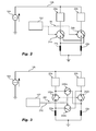
Figures 2 to 6 are circuit diagrams showing different embodiments of a lighting system according to the present invention. - In the following description, numerous specific details are given to provide a thorough understanding of embodiments. The embodiments can be practiced without one or more of the specific details, or with other methods, components, materials, etc. In other instances, well-known structures, materials, or operations are not shown or described in detail to avoid obscuring aspects of the embodiments.
- Reference throughout this specification to "one embodiment" or "an embodiment" means that a particular feature, structure, or characteristic described in connection with the embodiment is included in at least one embodiment. Thus, the appearances of the phrases "in one embodiment" or "in an embodiment" in various places throughout this specification are not necessarily all referring to the same embodiment. Furthermore, the particular features, structures, or characteristics may be combined in any suitable manner in one or more embodiments.
- The headings provided herein are for convenience only and do not interpret the scope or meaning of the embodiments.
-
Figure 2 shows an embodiment of an electronic converter 10 comprising apower circuit 104. Generally speaking, such a converter 10 may also comprisecontrol circuit 102,switch 108 and/orswitch 110, which have been previously described with reference toFigure 1 . - In various embodiments, power circuit 104 (for example an AC/DC or a DC/DC switching power supply) receives as input a supply signal (for example from the electric line) and outputs, through a
power output 106, a direct current. For example, in the considered embodiment electronic converter 10 supplies twoLED modules - In the considered embodiment, driver circuit 10 also comprises two
inductive elements - For example, in the considered embodiment, the switching of
electronic changeover switches control circuit 102, which actuates both switches 24a and 24b simultaneously through acommon control signal 26. - As a consequence, in a first operation time interval,
LED module 20a is connected in series withinductive element 22a, andLED module 20b is connected in series withinductive element 22b. Instead, in a second operation time interval,LED module 20a is connected in series withinductive element 22b, andLED module 20b is connected in series withinductive element 22a. - In an embodiment,
control circuit 102 is adapted to repeat such an operation time interval sequence periodically. - Therefore, the resistive load of LED strings, i.e. the voltage drops across LED junctions, are connected in an alternated fashion to
inductors inductors - Generally speaking, the value of the impedances and the switching frequency should be chosen while taking into account both the mechanical size of the components and the width of the oscillations.
- For example,
Figure 3 shows a first possible embodiment, wherein two electronic switches are used for each switching means 24a and 24b. - Specifically, in the considered embodiment, a
first switch 240a is connected betweenLED module 20a andinductor 22a, and asecond switch 242a is connected betweenLED module 20a andinductor 22b. Similarly, athird switch 240b is connected betweenLED module 20b andinductor 22b, and afourth switch 242b is connected betweenLED module 20b andinductor 22a. - As a consequence, during the first operation time interval (see for example
Figure 4a ), switches 240a and 240b are closed andswitches Figure 4b ), switches 240a and 240b are open andswitches switches synchronized control signals control circuit 102 comprises a two-phase clock generator, i.e. a clock generator which generates afirst clock signal 260 and asecond clock signal 262 which corresponds to an inverted first clock signal. -
Figure 5 shows a possible embodiment wherein power transistors, such as for example metal-oxide-semiconductor field-effect transistors (MOSFETs), are used asswitches - In an embodiment which is particularly useful for MOSFET transistor driving, the control circuit generates control signals 260 and 262 through a H-bridge driver. Such driver circuits for H bridges are known in the field of DC/AC and DC/DC switch-mode electronic converters, which makes a detailed description thereof unnecessary.
- In the previously considered embodiments, the switching means 24a and 24b and
inductors Figures 2 to 5 three connection wires are needed between converter 10 andLED modules - However, generally speaking both
control circuit 102 and switching means 24a and 24b, as well asinductors - Moreover, in case LED module(s) 20 should comprise a plurality of LED strings connected in parallel, switching means 24a and 24b and
inductors circuit 102 may be included into LED module. - The previously described Figures can also be applied to a higher number of LED strings.
- For example, if the number of LED strings is even, LED strings may be grouped into sets each comprising always and only two LED strings, and which are driven as previously described.
- On the contrary,
Figure 6 shows an embodiment which may also be used for any number of strings (an odd number as well). - Specifically, in the considered embodiment, a plurality of
LED strings respective inductor - Also in this case respective switching means 24a, 24b, ..., 24n (such as changeover switches) are associated to each
LED string - In general, switching means 24a, 24b, ..., 24n are adapted to selectively connect each LED string to a
respective inductor LED string first inductor LED string second inductor - For example, in the presently considered embodiment, the switching means are configured to form a closed loop, i.e. the
first LED string 20a may be connected to thefirst inductor 22a or to thesecond inductor 22b, thesecond LED string 20a may be connected to thesecond inductor 22b or to the third inductor, etc. On the contrary, thelast LED string 20n may be connected to thelast inductor 22n or to thefirst inductor 22a. - In general, in order to better distribute the current onto the LED strings, it is possible to provide further operation time intervals, wherein each LED string is connected to a respective inductor, which in the previous time intervals has not yet been connected in series with such a LED string.
- As a consequence, the previously described embodiments have several advantages, such as for example:
- in the case of two LED strings, the current generated via
generator 104 is distributed equally to both LED strings; - the use of inductors and/or changeover switches / switches introduces only small electric losses;
- a single current generator is sufficient and it is not necessary to use current regulators for each LED string, which makes it possible to use the described solution also in lighting systems already comprising a current generator;
- the control of the system is easy, and can be accomplished via a conventional two-phase clock generator;
- it is possible to distribute possible manufacturing tolerances of the various components (comprising the inductors as well) on the various branches, which makes the solution very stable; and
- the solution can be extended to any number of LED strings, for example by adding, for each further string, a new H-bridge circuit arrangement.
- Of course, without prejudice to the underlying principle of the invention, the details and the embodiments may vary, even appreciably, with respect to what has been described by way of non-limiting example only, without departing from the scope of the invention as defined by the annexed claims.
Claims (10)
- A circuit for driving a plurality of light sources (L) via a current generator (104), wherein said light sources (L) are grouped into a plurality of light source sets (20a, 20b, 20n), wherein the driver circuit comprises:- a plurality of inductive elements (22a, 22b, 22n);- a plurality of switching means (24a, 24b, 24n) adapted to selectively connect each light source set (20a, 20b, 20n) in series with one of said inductive elements (22a, 22b, 22n); and- a control circuit (102) configured for driving said plurality of switching means (24a, 24b, 24n), so thata) during a first operation time interval, each light source set (20a, 20b, 20n) is connected in series with a respective first inductive element (22a, 22b, 22n), andb) during a second operation time interval, each light source set (20a, 20b, 20n) is connected in series with a respective second inductive element (22a, 22b, 22n), wherein the respective second inductive element (22a, 22b, 22n) is separate from the respective first inductive element (22a, 22b, 22n).
- The driver circuit according to Claim 1, wherein the number of inductive elements (22a, 22b, 22n) corresponds to the number of said light source sets (20a, 20b, 20n).
- The driver circuit according to Claim 1 or Claim 2, wherein said switching means (24a, 24b, 24n) are changeover switches.
- The driver circuit according to Claim 3, wherein said control circuit (102) is configured for driving said changeover switches (24a, 24b, 24n) with a common control signal (26).
- The driver circuit according to Claim 1 or Claim 2, wherein each switching means (24a, 24b) comprises a respective first and a respective second electronic switch (240a, 242a; 240b, 242b), such as MOSFET transistors, and wherein said control circuit (102) is configured for driving said switching means (24a, 24b), so that:a) during said first operation time interval, the respective first switch (240a, 240b) of each switching means (24a, 24b) is closed and the respective second switch (242a, 242b) of each switching means (24a, 24b) is opened, andb) during said second operation time interval, the respective first switch (240a, 240b) of each switching means (24a, 24b) is opened and the respective second switch (242a, 242b) of each switching means (24a, 24b) is closed.
- The driver circuit according to Claim 5, wherein said control circuit (102) is configured for driving said first and second switches of said switching means (24a, 24b) with a respective first (260) and second (262) common control signal.
- The driver circuit according to Claim 5 or Claim 6, wherein said control circuit (102) comprises a two-phase clock generator and/or a H-bridge driver circuit.
- A lighting system comprising:- a plurality of light sources (L) grouped into a plurality of light source sets (20a, 20b, 20n);- a current generator (104) configured for powering said light source sets (20a, 20b, 20n) with a current; and- a driver circuit according to any of claims 1 to 7.
- The lighting system according to Claim 8, wherein each light source set is included in a respective LED module.
- A method of driving a plurality of light sources (L) via a current generator (104), wherein said light sources (L) are grouped into a plurality of light source sets (20a, 20b, 20n), the method comprising the steps of:- providing a plurality of inductive elements (22a, 22b, 22n);- providing a plurality of switching means (24a, 24b, 24n) adapted to selectively connect each light source set (20a, 20b, 20n) in series with one of said inductive elements (22a, 22b, 22n); and- driving (102) said plurality of switching means (24a, 24b, 24n), so thata) during a first operation time interval, each light source set (20a, 20b, 20n) is connected in series with a respective first inductive element (22a, 22b, 22n), andb) during a second operation time interval, each light source set (20a, 20b, 20n) is connected in series with a respective second inductive element (22a, 22b, 22n), wherein the respective second inductive element (22a, 22b, 22n) is separate from the respective first inductive element (22a, 22b, 22n).
Applications Claiming Priority (1)
| Application Number | Priority Date | Filing Date | Title |
|---|---|---|---|
| ITTO20110925 | 2011-10-14 |
Publications (2)
| Publication Number | Publication Date |
|---|---|
| EP2592907A1 true EP2592907A1 (en) | 2013-05-15 |
| EP2592907B1 EP2592907B1 (en) | 2015-08-12 |
Family
ID=44993789
Family Applications (1)
| Application Number | Title | Priority Date | Filing Date |
|---|---|---|---|
| EP12188088.4A Not-in-force EP2592907B1 (en) | 2011-10-14 | 2012-10-11 | A circuit for driving light sources, relative lighting system and method of driving light sources |
Country Status (4)
| Country | Link |
|---|---|
| US (2) | US8749150B2 (en) |
| EP (1) | EP2592907B1 (en) |
| KR (1) | KR20130040752A (en) |
| CN (1) | CN103052207B (en) |
Families Citing this family (2)
| Publication number | Priority date | Publication date | Assignee | Title |
|---|---|---|---|---|
| US9702618B2 (en) * | 2014-10-30 | 2017-07-11 | Electraled, Inc. | LED lighting array system for illuminating a display case |
| JP7335324B2 (en) * | 2018-08-17 | 2023-08-29 | シグニファイ ホールディング ビー ヴィ | LED drive circuit |
Citations (3)
| Publication number | Priority date | Publication date | Assignee | Title |
|---|---|---|---|---|
| DE102004032456B3 (en) * | 2004-06-30 | 2006-04-06 | Siemens Ag | Circuit arrangement for operating illuminated sign e.g. for railway safety installations, and motor vehicles, has constant current sources which are fed from common voltage source |
| WO2009039112A1 (en) * | 2007-09-21 | 2009-03-26 | Exclara, Inc. | Digital driver apparatus, method and system for solid state lighting |
| US20100033109A1 (en) * | 2008-08-05 | 2010-02-11 | O2Micro, Inc. | Driving circuit for powering light sources |
Family Cites Families (4)
| Publication number | Priority date | Publication date | Assignee | Title |
|---|---|---|---|---|
| US6798152B2 (en) * | 2002-08-21 | 2004-09-28 | Freescale Semiconductor, Inc. | Closed loop current control circuit and method thereof |
| KR100628718B1 (en) * | 2005-02-26 | 2006-09-28 | 삼성전자주식회사 | LED drive system |
| US7986107B2 (en) * | 2008-11-06 | 2011-07-26 | Lumenetix, Inc. | Electrical circuit for driving LEDs in dissimilar color string lengths |
| US8278837B1 (en) * | 2008-11-24 | 2012-10-02 | Switch Bulb Company, Inc. | Single inductor control of multi-color LED systems |
-
2012
- 2012-10-11 EP EP12188088.4A patent/EP2592907B1/en not_active Not-in-force
- 2012-10-12 CN CN201210387702.0A patent/CN103052207B/en not_active Expired - Fee Related
- 2012-10-12 US US13/650,183 patent/US8749150B2/en not_active Ceased
- 2012-10-15 KR KR1020120114191A patent/KR20130040752A/en not_active Abandoned
-
2015
- 2015-02-05 US US14/614,511 patent/USRE45966E1/en active Active
Patent Citations (3)
| Publication number | Priority date | Publication date | Assignee | Title |
|---|---|---|---|---|
| DE102004032456B3 (en) * | 2004-06-30 | 2006-04-06 | Siemens Ag | Circuit arrangement for operating illuminated sign e.g. for railway safety installations, and motor vehicles, has constant current sources which are fed from common voltage source |
| WO2009039112A1 (en) * | 2007-09-21 | 2009-03-26 | Exclara, Inc. | Digital driver apparatus, method and system for solid state lighting |
| US20100033109A1 (en) * | 2008-08-05 | 2010-02-11 | O2Micro, Inc. | Driving circuit for powering light sources |
Also Published As
| Publication number | Publication date |
|---|---|
| KR20130040752A (en) | 2013-04-24 |
| USRE45966E1 (en) | 2016-04-05 |
| US8749150B2 (en) | 2014-06-10 |
| US20130093337A1 (en) | 2013-04-18 |
| EP2592907B1 (en) | 2015-08-12 |
| CN103052207A (en) | 2013-04-17 |
| CN103052207B (en) | 2015-11-18 |
Similar Documents
| Publication | Publication Date | Title |
|---|---|---|
| US8710757B2 (en) | Power converter for an LED assembly and lighting application | |
| US9699844B2 (en) | Multichannel constant current LED driving circuit, driving method and LED driving power | |
| US9320093B2 (en) | Configurable LED driver/dimmer for solid state lighting applications | |
| US8310165B2 (en) | High-voltage LED drive scheme with partial power regulation | |
| US9374860B2 (en) | Lighting device | |
| ATE545193T1 (en) | CONTROL METHOD FOR PARALLEL-CONNECTED CURRENT TRANSFORMERS | |
| US9648677B2 (en) | LED driving circuit and method using single inductor | |
| TW201320816A (en) | LED current control | |
| US8716955B2 (en) | Constant current LED driver | |
| CN103108433A (en) | Voltage adjusting circuit and light emitting diode (LED) drive device thereof | |
| WO2016007263A1 (en) | System and method for achieving precise regulation of multiple outputs in a multi-resonant led driver stage | |
| US8779689B2 (en) | Ramp controlled driver for series/parallel solid state lighting devices | |
| US9408272B2 (en) | Light driver and the controller and driving method thereof | |
| EP2592907B1 (en) | A circuit for driving light sources, relative lighting system and method of driving light sources | |
| US9078317B1 (en) | Floating output voltage boost regulator driving LEDs using a buck controller | |
| US9369050B1 (en) | Indirect current sensing method for a constant current flyback converter | |
| JP5150742B2 (en) | LED drive circuit | |
| KR101694998B1 (en) | Apparatus for led power control | |
| CN120826981A (en) | Multi-channel light emitting diode, LED, driver and corresponding method, LED-based lighting device and computer program product | |
| EP2078445B1 (en) | A circuit for driving light sources and related method | |
| JP3191537U (en) | Light-emitting diode constant current drive | |
| US10485063B2 (en) | Power supply circuit, and related lighting system and method for operating a power supply circuit |
Legal Events
| Date | Code | Title | Description |
|---|---|---|---|
| PUAI | Public reference made under article 153(3) epc to a published international application that has entered the european phase |
Free format text: ORIGINAL CODE: 0009012 |
|
| AK | Designated contracting states |
Kind code of ref document: A1 Designated state(s): AL AT BE BG CH CY CZ DE DK EE ES FI FR GB GR HR HU IE IS IT LI LT LU LV MC MK MT NL NO PL PT RO RS SE SI SK SM TR |
|
| AX | Request for extension of the european patent |
Extension state: BA ME |
|
| 17P | Request for examination filed |
Effective date: 20131031 |
|
| RBV | Designated contracting states (corrected) |
Designated state(s): AL AT BE BG CH CY CZ DE DK EE ES FI FR GB GR HR HU IE IS IT LI LT LU LV MC MK MT NL NO PL PT RO RS SE SI SK SM TR |
|
| GRAP | Despatch of communication of intention to grant a patent |
Free format text: ORIGINAL CODE: EPIDOSNIGR1 |
|
| INTG | Intention to grant announced |
Effective date: 20150317 |
|
| GRAS | Grant fee paid |
Free format text: ORIGINAL CODE: EPIDOSNIGR3 |
|
| GRAA | (expected) grant |
Free format text: ORIGINAL CODE: 0009210 |
|
| AK | Designated contracting states |
Kind code of ref document: B1 Designated state(s): AL AT BE BG CH CY CZ DE DK EE ES FI FR GB GR HR HU IE IS IT LI LT LU LV MC MK MT NL NO PL PT RO RS SE SI SK SM TR |
|
| REG | Reference to a national code |
Ref country code: GB Ref legal event code: FG4D |
|
| REG | Reference to a national code |
Ref country code: CH Ref legal event code: EP |
|
| REG | Reference to a national code |
Ref country code: AT Ref legal event code: REF Ref document number: 743104 Country of ref document: AT Kind code of ref document: T Effective date: 20150815 |
|
| REG | Reference to a national code |
Ref country code: IE Ref legal event code: FG4D |
|
| REG | Reference to a national code |
Ref country code: DE Ref legal event code: R096 Ref document number: 602012009482 Country of ref document: DE |
|
| REG | Reference to a national code |
Ref country code: FR Ref legal event code: PLFP Year of fee payment: 4 |
|
| REG | Reference to a national code |
Ref country code: LT Ref legal event code: MG4D |
|
| REG | Reference to a national code |
Ref country code: NL Ref legal event code: MP Effective date: 20150812 |
|
| PG25 | Lapsed in a contracting state [announced via postgrant information from national office to epo] |
Ref country code: NO Free format text: LAPSE BECAUSE OF FAILURE TO SUBMIT A TRANSLATION OF THE DESCRIPTION OR TO PAY THE FEE WITHIN THE PRESCRIBED TIME-LIMIT Effective date: 20151112 Ref country code: LV Free format text: LAPSE BECAUSE OF FAILURE TO SUBMIT A TRANSLATION OF THE DESCRIPTION OR TO PAY THE FEE WITHIN THE PRESCRIBED TIME-LIMIT Effective date: 20150812 Ref country code: LT Free format text: LAPSE BECAUSE OF FAILURE TO SUBMIT A TRANSLATION OF THE DESCRIPTION OR TO PAY THE FEE WITHIN THE PRESCRIBED TIME-LIMIT Effective date: 20150812 Ref country code: GR Free format text: LAPSE BECAUSE OF FAILURE TO SUBMIT A TRANSLATION OF THE DESCRIPTION OR TO PAY THE FEE WITHIN THE PRESCRIBED TIME-LIMIT Effective date: 20151113 |
|
| PG25 | Lapsed in a contracting state [announced via postgrant information from national office to epo] |
Ref country code: PL Free format text: LAPSE BECAUSE OF FAILURE TO SUBMIT A TRANSLATION OF THE DESCRIPTION OR TO PAY THE FEE WITHIN THE PRESCRIBED TIME-LIMIT Effective date: 20150812 Ref country code: IS Free format text: LAPSE BECAUSE OF FAILURE TO SUBMIT A TRANSLATION OF THE DESCRIPTION OR TO PAY THE FEE WITHIN THE PRESCRIBED TIME-LIMIT Effective date: 20151212 Ref country code: SE Free format text: LAPSE BECAUSE OF FAILURE TO SUBMIT A TRANSLATION OF THE DESCRIPTION OR TO PAY THE FEE WITHIN THE PRESCRIBED TIME-LIMIT Effective date: 20150812 Ref country code: HR Free format text: LAPSE BECAUSE OF FAILURE TO SUBMIT A TRANSLATION OF THE DESCRIPTION OR TO PAY THE FEE WITHIN THE PRESCRIBED TIME-LIMIT Effective date: 20150812 Ref country code: RS Free format text: LAPSE BECAUSE OF FAILURE TO SUBMIT A TRANSLATION OF THE DESCRIPTION OR TO PAY THE FEE WITHIN THE PRESCRIBED TIME-LIMIT Effective date: 20150812 Ref country code: PT Free format text: LAPSE BECAUSE OF FAILURE TO SUBMIT A TRANSLATION OF THE DESCRIPTION OR TO PAY THE FEE WITHIN THE PRESCRIBED TIME-LIMIT Effective date: 20151214 Ref country code: ES Free format text: LAPSE BECAUSE OF FAILURE TO SUBMIT A TRANSLATION OF THE DESCRIPTION OR TO PAY THE FEE WITHIN THE PRESCRIBED TIME-LIMIT Effective date: 20150812 |
|
| PG25 | Lapsed in a contracting state [announced via postgrant information from national office to epo] |
Ref country code: NL Free format text: LAPSE BECAUSE OF FAILURE TO SUBMIT A TRANSLATION OF THE DESCRIPTION OR TO PAY THE FEE WITHIN THE PRESCRIBED TIME-LIMIT Effective date: 20150812 |
|
| PG25 | Lapsed in a contracting state [announced via postgrant information from national office to epo] |
Ref country code: DK Free format text: LAPSE BECAUSE OF FAILURE TO SUBMIT A TRANSLATION OF THE DESCRIPTION OR TO PAY THE FEE WITHIN THE PRESCRIBED TIME-LIMIT Effective date: 20150812 Ref country code: SK Free format text: LAPSE BECAUSE OF FAILURE TO SUBMIT A TRANSLATION OF THE DESCRIPTION OR TO PAY THE FEE WITHIN THE PRESCRIBED TIME-LIMIT Effective date: 20150812 Ref country code: EE Free format text: LAPSE BECAUSE OF FAILURE TO SUBMIT A TRANSLATION OF THE DESCRIPTION OR TO PAY THE FEE WITHIN THE PRESCRIBED TIME-LIMIT Effective date: 20150812 Ref country code: CZ Free format text: LAPSE BECAUSE OF FAILURE TO SUBMIT A TRANSLATION OF THE DESCRIPTION OR TO PAY THE FEE WITHIN THE PRESCRIBED TIME-LIMIT Effective date: 20150812 |
|
| REG | Reference to a national code |
Ref country code: DE Ref legal event code: R097 Ref document number: 602012009482 Country of ref document: DE |
|
| PG25 | Lapsed in a contracting state [announced via postgrant information from national office to epo] |
Ref country code: RO Free format text: LAPSE BECAUSE OF FAILURE TO SUBMIT A TRANSLATION OF THE DESCRIPTION OR TO PAY THE FEE WITHIN THE PRESCRIBED TIME-LIMIT Effective date: 20150812 Ref country code: LU Free format text: LAPSE BECAUSE OF FAILURE TO SUBMIT A TRANSLATION OF THE DESCRIPTION OR TO PAY THE FEE WITHIN THE PRESCRIBED TIME-LIMIT Effective date: 20151011 |
|
| REG | Reference to a national code |
Ref country code: CH Ref legal event code: PL |
|
| PLBE | No opposition filed within time limit |
Free format text: ORIGINAL CODE: 0009261 |
|
| STAA | Information on the status of an ep patent application or granted ep patent |
Free format text: STATUS: NO OPPOSITION FILED WITHIN TIME LIMIT |
|
| PG25 | Lapsed in a contracting state [announced via postgrant information from national office to epo] |
Ref country code: MC Free format text: LAPSE BECAUSE OF FAILURE TO SUBMIT A TRANSLATION OF THE DESCRIPTION OR TO PAY THE FEE WITHIN THE PRESCRIBED TIME-LIMIT Effective date: 20150812 |
|
| 26N | No opposition filed |
Effective date: 20160513 |
|
| REG | Reference to a national code |
Ref country code: IE Ref legal event code: MM4A |
|
| PG25 | Lapsed in a contracting state [announced via postgrant information from national office to epo] |
Ref country code: LI Free format text: LAPSE BECAUSE OF NON-PAYMENT OF DUE FEES Effective date: 20151031 Ref country code: CH Free format text: LAPSE BECAUSE OF NON-PAYMENT OF DUE FEES Effective date: 20151031 |
|
| PG25 | Lapsed in a contracting state [announced via postgrant information from national office to epo] |
Ref country code: SI Free format text: LAPSE BECAUSE OF FAILURE TO SUBMIT A TRANSLATION OF THE DESCRIPTION OR TO PAY THE FEE WITHIN THE PRESCRIBED TIME-LIMIT Effective date: 20150812 |
|
| REG | Reference to a national code |
Ref country code: FR Ref legal event code: PLFP Year of fee payment: 5 |
|
| PG25 | Lapsed in a contracting state [announced via postgrant information from national office to epo] |
Ref country code: IE Free format text: LAPSE BECAUSE OF NON-PAYMENT OF DUE FEES Effective date: 20151011 |
|
| PG25 | Lapsed in a contracting state [announced via postgrant information from national office to epo] |
Ref country code: BE Free format text: LAPSE BECAUSE OF FAILURE TO SUBMIT A TRANSLATION OF THE DESCRIPTION OR TO PAY THE FEE WITHIN THE PRESCRIBED TIME-LIMIT Effective date: 20150812 |
|
| PG25 | Lapsed in a contracting state [announced via postgrant information from national office to epo] |
Ref country code: SM Free format text: LAPSE BECAUSE OF FAILURE TO SUBMIT A TRANSLATION OF THE DESCRIPTION OR TO PAY THE FEE WITHIN THE PRESCRIBED TIME-LIMIT Effective date: 20150812 Ref country code: BG Free format text: LAPSE BECAUSE OF FAILURE TO SUBMIT A TRANSLATION OF THE DESCRIPTION OR TO PAY THE FEE WITHIN THE PRESCRIBED TIME-LIMIT Effective date: 20150812 Ref country code: HU Free format text: LAPSE BECAUSE OF FAILURE TO SUBMIT A TRANSLATION OF THE DESCRIPTION OR TO PAY THE FEE WITHIN THE PRESCRIBED TIME-LIMIT; INVALID AB INITIO Effective date: 20121011 |
|
| GBPC | Gb: european patent ceased through non-payment of renewal fee |
Effective date: 20161011 |
|
| PG25 | Lapsed in a contracting state [announced via postgrant information from national office to epo] |
Ref country code: CY Free format text: LAPSE BECAUSE OF FAILURE TO SUBMIT A TRANSLATION OF THE DESCRIPTION OR TO PAY THE FEE WITHIN THE PRESCRIBED TIME-LIMIT Effective date: 20150812 |
|
| PG25 | Lapsed in a contracting state [announced via postgrant information from national office to epo] |
Ref country code: GB Free format text: LAPSE BECAUSE OF NON-PAYMENT OF DUE FEES Effective date: 20161011 |
|
| PG25 | Lapsed in a contracting state [announced via postgrant information from national office to epo] |
Ref country code: MT Free format text: LAPSE BECAUSE OF FAILURE TO SUBMIT A TRANSLATION OF THE DESCRIPTION OR TO PAY THE FEE WITHIN THE PRESCRIBED TIME-LIMIT Effective date: 20150812 |
|
| REG | Reference to a national code |
Ref country code: FR Ref legal event code: PLFP Year of fee payment: 6 |
|
| PGFP | Annual fee paid to national office [announced via postgrant information from national office to epo] |
Ref country code: DE Payment date: 20171019 Year of fee payment: 6 Ref country code: FI Payment date: 20171020 Year of fee payment: 6 Ref country code: FR Payment date: 20171024 Year of fee payment: 6 |
|
| PGFP | Annual fee paid to national office [announced via postgrant information from national office to epo] |
Ref country code: AT Payment date: 20171020 Year of fee payment: 6 Ref country code: IT Payment date: 20171023 Year of fee payment: 6 |
|
| REG | Reference to a national code |
Ref country code: AT Ref legal event code: UEP Ref document number: 743104 Country of ref document: AT Kind code of ref document: T Effective date: 20150812 |
|
| PG25 | Lapsed in a contracting state [announced via postgrant information from national office to epo] |
Ref country code: MK Free format text: LAPSE BECAUSE OF FAILURE TO SUBMIT A TRANSLATION OF THE DESCRIPTION OR TO PAY THE FEE WITHIN THE PRESCRIBED TIME-LIMIT Effective date: 20150812 Ref country code: TR Free format text: LAPSE BECAUSE OF FAILURE TO SUBMIT A TRANSLATION OF THE DESCRIPTION OR TO PAY THE FEE WITHIN THE PRESCRIBED TIME-LIMIT Effective date: 20150812 |
|
| PG25 | Lapsed in a contracting state [announced via postgrant information from national office to epo] |
Ref country code: AL Free format text: LAPSE BECAUSE OF FAILURE TO SUBMIT A TRANSLATION OF THE DESCRIPTION OR TO PAY THE FEE WITHIN THE PRESCRIBED TIME-LIMIT Effective date: 20150812 |
|
| REG | Reference to a national code |
Ref country code: DE Ref legal event code: R119 Ref document number: 602012009482 Country of ref document: DE |
|
| REG | Reference to a national code |
Ref country code: AT Ref legal event code: MM01 Ref document number: 743104 Country of ref document: AT Kind code of ref document: T Effective date: 20181011 |
|
| PG25 | Lapsed in a contracting state [announced via postgrant information from national office to epo] |
Ref country code: FI Free format text: LAPSE BECAUSE OF NON-PAYMENT OF DUE FEES Effective date: 20181011 Ref country code: DE Free format text: LAPSE BECAUSE OF NON-PAYMENT OF DUE FEES Effective date: 20190501 |
|
| PG25 | Lapsed in a contracting state [announced via postgrant information from national office to epo] |
Ref country code: FR Free format text: LAPSE BECAUSE OF NON-PAYMENT OF DUE FEES Effective date: 20181031 |
|
| PG25 | Lapsed in a contracting state [announced via postgrant information from national office to epo] |
Ref country code: IT Free format text: LAPSE BECAUSE OF NON-PAYMENT OF DUE FEES Effective date: 20181011 Ref country code: AT Free format text: LAPSE BECAUSE OF NON-PAYMENT OF DUE FEES Effective date: 20181011 |