EP2592652A2 - Variable capacitor circuit and method - Google Patents
Variable capacitor circuit and method Download PDFInfo
- Publication number
- EP2592652A2 EP2592652A2 EP12007611.2A EP12007611A EP2592652A2 EP 2592652 A2 EP2592652 A2 EP 2592652A2 EP 12007611 A EP12007611 A EP 12007611A EP 2592652 A2 EP2592652 A2 EP 2592652A2
- Authority
- EP
- European Patent Office
- Prior art keywords
- variable capacitor
- capacitor circuit
- mos
- voltage signal
- equivalent capacitance
- Prior art date
- Legal status (The legal status is an assumption and is not a legal conclusion. Google has not performed a legal analysis and makes no representation as to the accuracy of the status listed.)
- Granted
Links
Images

Classifications
-
- A—HUMAN NECESSITIES
- A61—MEDICAL OR VETERINARY SCIENCE; HYGIENE
- A61B—DIAGNOSIS; SURGERY; IDENTIFICATION
- A61B5/00—Measuring for diagnostic purposes; Identification of persons
- A61B5/72—Signal processing specially adapted for physiological signals or for diagnostic purposes
- A61B5/7203—Signal processing specially adapted for physiological signals or for diagnostic purposes for noise prevention, reduction or removal
- A61B5/7207—Signal processing specially adapted for physiological signals or for diagnostic purposes for noise prevention, reduction or removal of noise induced by motion artifacts
- A61B5/7214—Signal processing specially adapted for physiological signals or for diagnostic purposes for noise prevention, reduction or removal of noise induced by motion artifacts using signal cancellation, e.g. based on input of two identical physiological sensors spaced apart, or based on two signals derived from the same sensor, for different optical wavelengths
-
- A—HUMAN NECESSITIES
- A61—MEDICAL OR VETERINARY SCIENCE; HYGIENE
- A61B—DIAGNOSIS; SURGERY; IDENTIFICATION
- A61B5/00—Measuring for diagnostic purposes; Identification of persons
- A61B5/05—Detecting, measuring or recording for diagnosis by means of electric currents or magnetic fields; Measuring using microwaves or radio waves
- A61B5/053—Measuring electrical impedance or conductance of a portion of the body
- A61B5/0531—Measuring skin impedance
-
- A—HUMAN NECESSITIES
- A61—MEDICAL OR VETERINARY SCIENCE; HYGIENE
- A61B—DIAGNOSIS; SURGERY; IDENTIFICATION
- A61B5/00—Measuring for diagnostic purposes; Identification of persons
- A61B5/24—Detecting, measuring or recording bioelectric or biomagnetic signals of the body or parts thereof
- A61B5/316—Modalities, i.e. specific diagnostic methods
- A61B5/318—Heart-related electrical modalities, e.g. electrocardiography [ECG]
- A61B5/346—Analysis of electrocardiograms
-
- H—ELECTRICITY
- H03—ELECTRONIC CIRCUITRY
- H03F—AMPLIFIERS
- H03F1/00—Details of amplifiers with only discharge tubes, only semiconductor devices or only unspecified devices as amplifying elements
- H03F1/56—Modifications of input or output impedances, not otherwise provided for
-
- H—ELECTRICITY
- H03—ELECTRONIC CIRCUITRY
- H03F—AMPLIFIERS
- H03F3/00—Amplifiers with only discharge tubes or only semiconductor devices as amplifying elements
- H03F3/45—Differential amplifiers
- H03F3/45071—Differential amplifiers with semiconductor devices only
- H03F3/45076—Differential amplifiers with semiconductor devices only characterised by the way of implementation of the active amplifying circuit in the differential amplifier
- H03F3/45475—Differential amplifiers with semiconductor devices only characterised by the way of implementation of the active amplifying circuit in the differential amplifier using IC blocks as the active amplifying circuit
-
- H—ELECTRICITY
- H10—SEMICONDUCTOR DEVICES; ELECTRIC SOLID-STATE DEVICES NOT OTHERWISE PROVIDED FOR
- H10D—INORGANIC ELECTRIC SEMICONDUCTOR DEVICES
- H10D84/00—Integrated devices formed in or on semiconductor substrates that comprise only semiconducting layers, e.g. on Si wafers or on GaAs-on-Si wafers
- H10D84/201—Integrated devices formed in or on semiconductor substrates that comprise only semiconducting layers, e.g. on Si wafers or on GaAs-on-Si wafers characterised by the integration of only components covered by H10D1/00 or H10D8/00, e.g. RLC circuits
- H10D84/204—Integrated devices formed in or on semiconductor substrates that comprise only semiconducting layers, e.g. on Si wafers or on GaAs-on-Si wafers characterised by the integration of only components covered by H10D1/00 or H10D8/00, e.g. RLC circuits of combinations of diodes or capacitors or resistors
- H10D84/212—Integrated devices formed in or on semiconductor substrates that comprise only semiconducting layers, e.g. on Si wafers or on GaAs-on-Si wafers characterised by the integration of only components covered by H10D1/00 or H10D8/00, e.g. RLC circuits of combinations of diodes or capacitors or resistors of only capacitors
- H10D84/217—Integrated devices formed in or on semiconductor substrates that comprise only semiconducting layers, e.g. on Si wafers or on GaAs-on-Si wafers characterised by the integration of only components covered by H10D1/00 or H10D8/00, e.g. RLC circuits of combinations of diodes or capacitors or resistors of only capacitors of only conductor-insulator-semiconductor capacitors
-
- H—ELECTRICITY
- H03—ELECTRONIC CIRCUITRY
- H03F—AMPLIFIERS
- H03F2200/00—Indexing scheme relating to amplifiers
- H03F2200/213—A variable capacitor being added in the input circuit, e.g. base, gate, of an amplifier stage
-
- H—ELECTRICITY
- H03—ELECTRONIC CIRCUITRY
- H03F—AMPLIFIERS
- H03F2200/00—Indexing scheme relating to amplifiers
- H03F2200/261—Amplifier which being suitable for instrumentation applications
-
- H—ELECTRICITY
- H03—ELECTRONIC CIRCUITRY
- H03F—AMPLIFIERS
- H03F2203/00—Indexing scheme relating to amplifiers with only discharge tubes or only semiconductor devices as amplifying elements covered by H03F3/00
- H03F2203/45—Indexing scheme relating to differential amplifiers
- H03F2203/45538—Indexing scheme relating to differential amplifiers the IC comprising balancing means, e.g. trimming means
-
- H—ELECTRICITY
- H03—ELECTRONIC CIRCUITRY
- H03F—AMPLIFIERS
- H03F2203/00—Indexing scheme relating to amplifiers with only discharge tubes or only semiconductor devices as amplifying elements covered by H03F3/00
- H03F2203/45—Indexing scheme relating to differential amplifiers
- H03F2203/45544—Indexing scheme relating to differential amplifiers the IC comprising one or more capacitors, e.g. coupling capacitors
-
- H—ELECTRICITY
- H03—ELECTRONIC CIRCUITRY
- H03F—AMPLIFIERS
- H03F2203/00—Indexing scheme relating to amplifiers with only discharge tubes or only semiconductor devices as amplifying elements covered by H03F3/00
- H03F2203/45—Indexing scheme relating to differential amplifiers
- H03F2203/45548—Indexing scheme relating to differential amplifiers the IC comprising one or more capacitors as shunts to earth or as short circuit between inputs
-
- H—ELECTRICITY
- H03—ELECTRONIC CIRCUITRY
- H03F—AMPLIFIERS
- H03F2203/00—Indexing scheme relating to amplifiers with only discharge tubes or only semiconductor devices as amplifying elements covered by H03F3/00
- H03F2203/45—Indexing scheme relating to differential amplifiers
- H03F2203/45576—Indexing scheme relating to differential amplifiers the IC comprising input impedance adapting or controlling means
Definitions
- the present disclosure is related to electrical circuits and more specifically to a variable capacitor circuit and a method for compensating a capacitance mismatch using the same.
- Variable capacitor arrays known in the art are described, for example, in US Patent Application 2007/026872 A1 .
- the proposed solution comprises, among other drawbacks, the use of on-off switches which are not suitable for capacitance mismatch compensation in certain biomedical signal acquisition circuits, such as circuits for the measurement and analysis of ECG or EEG signals.
- a variable capacitor circuit comprising a plurality of MOS capacitors, each MOS capacitor being implemented by a MOS transistor with the gate terminal connected to a first voltage signal and with the drain terminal shorted with the source terminal and connected to a second voltage signal, said MOS capacitors being connected in parallel through the gate terminal connected to the first voltage signal, and being operated in a cut-off region in which the equivalent capacitance of each MOS capacitor remains substantially constant for variations of the first voltage signal.
- the value of the second voltage signal restricted to two voltage values lying within the cut-off region.
- the values of the second voltage signal are 0V or 0.5V.
- the two values are chosen such that the equivalent capacitance of each MOS capacitor varies in the sub femtoFarad range.
- the total equivalent capacitance of the variable capacitor circuit is controlled by a digital signal.
- the MOS capacitors of the variable capacitor circuit are implemented with binary scaled sizes such that the equivalent capacitance of the MOS capacitors follows a binary arrangement.
- the MOS transistor is a pMOs transistor and is operated for first voltage signals close to a ground rail satisfying the cut-off requirement.
- the MOS transistor is an nMOs transistor and is operated for first voltage signals close to a positive supply rail.
- a biomedical signal acquisition circuit comprising an instrumentation amplifier and a variable capacitor circuit according to an exemplary embodiment of the invention connected to each input line of the instrumentation amplifier.
- the variable capacitor circuit is connected to the input line of the instrumentation amplifier through the first voltage signal terminal.
- a method for compensating a capacitance mismatch between the input lines of an instrumentation amplifier comprising: connecting a variable capacitor circuit according to an exemplary embodiment of the invention to each input line of the instrumentation amplifier and changing the equivalent capacitance of the variable capacitor circuit so as to balance the parasitic loads on both input lines.
- the step of changing the equivalent capacitance of the variable capacitor circuit is done by applying a digital signal to variable capacitor circuit.
- variable capacitor circuit for capacitance mismatch compensation in a biomedical signal acquisition system.
- FIG 1 shows a first example embodiment of a variable capacitor circuit 100 according to the invention, comprising a plurality of variable MOS capacitors 110 connected in parallel.
- Each MOS capacitor 110 is driven by control voltage Vc and a signal voltage Vs.
- the signal voltage Vs is connected to the gate, while the drain and source are shorted to the control voltage Vc.
- Each MOS capacitor 110 presents an equivalent capacitance C that depends on the values of the control voltage Vc and the signal voltage Vs as shown in Figure 2 .
- the MOS transistor is operated in the cut-off region 120, so that its equivalent capacitance C is small and remains substantially independent of the signal voltage Vs.
- the equivalent capacitance C of a MOS capacitor 110 when operated in the cut-off region 120, remains substantially constant for large variations of the signal voltage Vs, for example even for a signal voltage Vs greater than 300 mVpp.
- the equivalent capacitance difference between two operating regions in the cut-off region 120 can be made to lie in the sub femtoFarad (fF) range, and for example, as small as 0.1fF.
- the control voltage Vc of each MOS capacitor 110 of the variable capacitor circuit 100 is restricted to just two voltage values within the cut-off region 120.
- the control voltage Vc for each MOS transistor can be chosen to be either a first value of, for example 0V, or a second value of, for example 0.5V, so that the equivalent capacitance of each MOS capacitor 110 is either a first equivalent capacitance Ca, e.g. of 2.2 fF, when the control voltage Vc is 0V, or a second equivalent capacitance Cb, e.g. of 2.3 fF, when the control voltage Vc is 0.5V.
- the equivalent capacitance difference presented by the MOS capacitors 110 when operated with a first or a second control voltage value is of 0.1 fF.
- the total equivalent capacitance of the variable capacitor circuit 100 can be controlled by a digital signal applied to the control voltage Vc input of the MOS transistors, so that their equivalent capacitance can be switched between two capacitance values.
- the capacitance value is Ci,0, if Vci is high, the capacitance value will be Ci,0 + ⁇ Ci.
- the difference between these two values ⁇ Ci can be made very small thus advantageously yielding a tunable variable capacitor circuit 100 with a sub-femtoFarad accuracy.
- the MOS capacitors 110 are implemented as pMOS transistors, in which the corresponding behavior according an example embodiment of the invention shown with reference to Figure 2 is achieved when operated for input signal levels close to the ground rail satisfying the cut-off requirement.
- the MOS capacitors 110 may be implemented as nMOS transistors, when operated for input signal levels closer to the positive supply rail.
- a variable capacitor circuit 100 may function as an ultra-precise tunable capacitor achieving a capacitance resolution in the range of sub femtoFarads.
- said tunable capacitance may be digitally controlled.
- the variable capacitor circuit 100 advantageously behaves as a linear capacitor without significant capacitance changes for large variations of the input voltage signal Vs.
- the variable capacitor circuit 100 may be implemented with minimal routing and area overhead.
- the variable capacitor circuit 100 allows for compensation of capacitance mismatch by capacitance tuning after the electrical circuit manufacturing process.
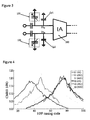
- FIG. 3 shows an exemplary application according to an example embodiment of the invention, in which an instrumentation amplifier 200 uses two variable capacitor circuits 100 to reduce the capacitance mismatch between the input lines inp, inn to that instrumentation amplifier 200.
- Capacitance mismatch between input lines to instrumentation amplifiers due to parasitic capacitances Cp1, Cp2 is a typical problem in biomedical signal acquisition circuits, and can be solved, according to an example embodiment of the invention, by adding a variable capacitor circuit 100 to each instrumentation amplifier input line, in order to balance the parasitic loads on both input lines.
- the variable capacitor circuit 100 is connected to the input line of the instrumentation amplifier through the voltage signal Vs terminal, so that the signals flowing through the input line do not affect the equivalent capacitance of variable capacitor circuit 100.
- the variable capacitor circuit 100 does not introduce any non-linear characteristics to the signal path when the equivalent capacitance is changed or tuned.
- variable capacitor circuits 100 is tuned in capacitance value to compensate parasitic mismatch and maximize the common-mode rejection ratio (CMRR).
- CMRR common-mode rejection ratio
- Figure 4 shows how the CMRR can be tuned after manufacturing. It illustrates the measured CMRR for two samples as a function of the digital control code of the variable capacitor circuits 100. Within the 0-40° C temperature range, the optimum value shifts slightly but still 115 dB can be guaranteed. Alternatively a periodic recalibration based on a temperature measurement and a LUT could be implemented.
Landscapes
- Health & Medical Sciences (AREA)
- Life Sciences & Earth Sciences (AREA)
- Engineering & Computer Science (AREA)
- Molecular Biology (AREA)
- Animal Behavior & Ethology (AREA)
- Veterinary Medicine (AREA)
- Public Health (AREA)
- Physics & Mathematics (AREA)
- General Health & Medical Sciences (AREA)
- Biophysics (AREA)
- Pathology (AREA)
- Biomedical Technology (AREA)
- Heart & Thoracic Surgery (AREA)
- Medical Informatics (AREA)
- Surgery (AREA)
- Signal Processing (AREA)
- Power Engineering (AREA)
- Cardiology (AREA)
- Psychiatry (AREA)
- Physiology (AREA)
- Artificial Intelligence (AREA)
- Computer Vision & Pattern Recognition (AREA)
- Dermatology (AREA)
- Nuclear Medicine, Radiotherapy & Molecular Imaging (AREA)
- Radiology & Medical Imaging (AREA)
- Amplifiers (AREA)
- Measurement And Recording Of Electrical Phenomena And Electrical Characteristics Of The Living Body (AREA)
- Networks Using Active Elements (AREA)
Abstract
Description
- The present disclosure is related to electrical circuits and more specifically to a variable capacitor circuit and a method for compensating a capacitance mismatch using the same.
- Variable capacitor arrays known in the art are described, for example, in
US Patent Application 2007/026872 A1 . However, the proposed solution comprises, among other drawbacks, the use of on-off switches which are not suitable for capacitance mismatch compensation in certain biomedical signal acquisition circuits, such as circuits for the measurement and analysis of ECG or EEG signals. - According to an example embodiment of the present disclosure there is provided a variable capacitor circuit comprising a plurality of MOS capacitors, each MOS capacitor being implemented by a MOS transistor with the gate terminal connected to a first voltage signal and with the drain terminal shorted with the source terminal and connected to a second voltage signal, said MOS capacitors being connected in parallel through the gate terminal connected to the first voltage signal, and being operated in a cut-off region in which the equivalent capacitance of each MOS capacitor remains substantially constant for variations of the first voltage signal.
- According to an example embodiment, the value of the second voltage signal restricted to two voltage values lying within the cut-off region. According to another example embodiment, the values of the second voltage signal are 0V or 0.5V. According to still another embodiment, the two values are chosen such that the equivalent capacitance of each MOS capacitor varies in the sub femtoFarad range. According to still another example embodiment, the total equivalent capacitance of the variable capacitor circuit is controlled by a digital signal.
- According to another example embodiment, the MOS capacitors of the variable capacitor circuit are implemented with binary scaled sizes such that the equivalent capacitance of the MOS capacitors follows a binary arrangement.
- According to still another example embodiment, the MOS transistor is a pMOs transistor and is operated for first voltage signals close to a ground rail satisfying the cut-off requirement. According to another example embodiment, the MOS transistor is an nMOs transistor and is operated for first voltage signals close to a positive supply rail.
- According to another example embodiment, there is provided a biomedical signal acquisition circuit comprising an instrumentation amplifier and a variable capacitor circuit according to an exemplary embodiment of the invention connected to each input line of the instrumentation amplifier. According to still another example embodiment, the variable capacitor circuit is connected to the input line of the instrumentation amplifier through the first voltage signal terminal.
- According to another example embodiment, there is provided a method for compensating a capacitance mismatch between the input lines of an instrumentation amplifier, the method comprising: connecting a variable capacitor circuit according to an exemplary embodiment of the invention to each input line of the instrumentation amplifier and changing the equivalent capacitance of the variable capacitor circuit so as to balance the parasitic loads on both input lines. According to still an example embodiment, the step of changing the equivalent capacitance of the variable capacitor circuit is done by applying a digital signal to variable capacitor circuit.
- According to another example embodiment, there is provided a use of a variable capacitor circuit according to any embodiment herein described, for capacitance mismatch compensation in a biomedical signal acquisition system.
- These as well as other aspects, advantages, and alternatives, will become apparent to those of ordinary skill in the art by reading the following detailed description, with reference where appropriate to the accompanying drawings.
- The disclosure will be further elucidated by means of the following description and the appended figures. Various exemplary embodiments are described herein with reference to the following figures, wherein like numerals denote like entities. The figures described are schematic and are non-limiting. Further, any reference signs in the claims shall not be construed as limiting the scope of the present disclosure. Still further, in the different figures, the same reference signs refer to the same or analogous elements.
-
Figure 1 shows a first example embodiment of a variable capacitor circuit according to the invention. -
Figure 2 shows an equivalent capacitance of a MOS transistor as a function of several voltage signals. -
Figure 3 shows an instrumentation amplifier with a variable capacitor circuit according to the invention to maximize the CMRR. -
Figure 4 illustrates the measured CMRR for two samples as a function of the digital control code of the variable capacitor circuit according to an example of the invention. -
Figure 1 shows a first example embodiment of avariable capacitor circuit 100 according to the invention, comprising a plurality ofvariable MOS capacitors 110 connected in parallel. EachMOS capacitor 110 is driven by control voltage Vc and a signal voltage Vs. The signal voltage Vs is connected to the gate, while the drain and source are shorted to the control voltage Vc. EachMOS capacitor 110 presents an equivalent capacitance C that depends on the values of the control voltage Vc and the signal voltage Vs as shown inFigure 2 . - According to an example embodiment of the invention, the MOS transistor is operated in the cut-off
region 120, so that its equivalent capacitance C is small and remains substantially independent of the signal voltage Vs. According to an example embodiment of the invention, the equivalent capacitance C of aMOS capacitor 110, when operated in the cut-offregion 120, remains substantially constant for large variations of the signal voltage Vs, for example even for a signal voltage Vs greater than 300 mVpp. According to another example embodiment of the invention the equivalent capacitance difference between two operating regions in the cut-offregion 120 can be made to lie in the sub femtoFarad (fF) range, and for example, as small as 0.1fF. - According to another example embodiment of the invention, the control voltage Vc of each
MOS capacitor 110 of thevariable capacitor circuit 100 is restricted to just two voltage values within the cut-offregion 120. According to one example embodiment the control voltage Vc for each MOS transistor can be chosen to be either a first value of, for example 0V, or a second value of, for example 0.5V, so that the equivalent capacitance of eachMOS capacitor 110 is either a first equivalent capacitance Ca, e.g. of 2.2 fF, when the control voltage Vc is 0V, or a second equivalent capacitance Cb, e.g. of 2.3 fF, when the control voltage Vc is 0.5V. It shall be then noted that, according to the example embodiment, the equivalent capacitance difference presented by theMOS capacitors 110 when operated with a first or a second control voltage value is of 0.1 fF. This advantageously allows for digital control and/or for a dynamical change or tuning of the equivalent capacitance presented by thevariable capacitor circuit 100 according to an example of the invention. According to an example embodiment, the total equivalent capacitance of thevariable capacitor circuit 100 can be controlled by a digital signal applied to the control voltage Vc input of the MOS transistors, so that their equivalent capacitance can be switched between two capacitance values. - According to another example embodiment of the invention, the
MOS capacitors 110 of thevariable capacitor circuit 100 are implemented with binary scaled sizes so that the equivalent capacitance of the MOS capacitors follows a binary arrangement, for example, C1=Co, C2=2Co, C3=4Co, C4= 8Co, C5=16Co, and so on. - According to another example embodiment of the invention, the total equivalent capacitance value Ctot of the
variable capacitor circuit 100 is given by:
where

- If the digital control signal Vci is low, the capacitance value is Ci,0, if Vci is high, the capacitance value will be Ci,0 + ΔCi. According to another example embodiment, the difference between these two values ΔCi can be made very small thus advantageously yielding a tunable
variable capacitor circuit 100 with a sub-femtoFarad accuracy. - According to an example embodiment of the invention, the
MOS capacitors 110 are implemented as pMOS transistors, in which the corresponding behavior according an example embodiment of the invention shown with reference toFigure 2 is achieved when operated for input signal levels close to the ground rail satisfying the cut-off requirement. According to another example embodiment of the invention, theMOS capacitors 110 may be implemented as nMOS transistors, when operated for input signal levels closer to the positive supply rail. - According to an example embodiment of the invention, a
variable capacitor circuit 100 may function as an ultra-precise tunable capacitor achieving a capacitance resolution in the range of sub femtoFarads. According to another example embodiment, said tunable capacitance may be digitally controlled. According to another example embodiment, thevariable capacitor circuit 100 advantageously behaves as a linear capacitor without significant capacitance changes for large variations of the input voltage signal Vs. According to another example embodiment, thevariable capacitor circuit 100 may be implemented with minimal routing and area overhead. According to another example embodiment, thevariable capacitor circuit 100 allows for compensation of capacitance mismatch by capacitance tuning after the electrical circuit manufacturing process. -
Figure 3 shows an exemplary application according to an example embodiment of the invention, in which aninstrumentation amplifier 200 uses twovariable capacitor circuits 100 to reduce the capacitance mismatch between the input lines inp, inn to thatinstrumentation amplifier 200. Capacitance mismatch between input lines to instrumentation amplifiers due to parasitic capacitances Cp1, Cp2 is a typical problem in biomedical signal acquisition circuits, and can be solved, according to an example embodiment of the invention, by adding avariable capacitor circuit 100 to each instrumentation amplifier input line, in order to balance the parasitic loads on both input lines. Advantageously, thevariable capacitor circuit 100 is connected to the input line of the instrumentation amplifier through the voltage signal Vs terminal, so that the signals flowing through the input line do not affect the equivalent capacitance ofvariable capacitor circuit 100. Also advantageously, thevariable capacitor circuit 100 does not introduce any non-linear characteristics to the signal path when the equivalent capacitance is changed or tuned. - According to an example embodiment of the invention, after manufacturing process of a biomedical signal acquisition circuit comprising an
instrumentation amplifier 200 and avariable capacitor circuit 100 connected to each input line of the instrumentation amplifier, thevariable capacitor circuits 100 is tuned in capacitance value to compensate parasitic mismatch and maximize the common-mode rejection ratio (CMRR). -
Figure 4 shows how the CMRR can be tuned after manufacturing. It illustrates the measured CMRR for two samples as a function of the digital control code of thevariable capacitor circuits 100. Within the 0-40° C temperature range, the optimum value shifts slightly but still 115 dB can be guaranteed. Alternatively a periodic recalibration based on a temperature measurement and a LUT could be implemented.
Claims (13)
- A variable capacitor circuit (100) comprising a plurality of MOS capacitors (110), each MOS capacitor being implemented by a MOS transistor with the gate terminal connected to a first voltage signal (Vs) and with the drain terminal shorted with the source terminal and connected to a second voltage signal (Vc), said MOS capacitors being connected in parallel through the gate terminal connected to the first voltage signal (Vs), and being operated in a cut-off region (120) in which the equivalent capacitance (C) of each MOS capacitor remains substantially constant for variations of the first voltage signal.
- The variable capacitor circuit of claim 1, wherein the value of the second voltage signal (Vc) is restricted to two voltage values lying within the cut-off region (120).
- The variable capacitor circuit of claim 2, wherein said values of the second voltage signal (Vc) are 0V or 0.5V.
- The variable capacitor circuit of claim 2, wherein said two values are chosen such that the equivalent capacitance (C) of each MOS capacitor varies in the sub femtoFarad range.
- The variable capacitor circuit of any of claims 2 to 4, wherein the total equivalent capacitance of the variable capacitor circuit is controlled by a digital signal.
- The variable capacitor circuit according to any of the preceding claims, wherein the MOS capacitors (110) of the variable capacitor circuit are implemented with binary scaled sizes such that the equivalent capacitance of the MOS capacitors follows a binary arrangement.
- The variable capacitor circuit according to any of claims 1 to 5, wherein the MOS transistor is a pMOs transistor and is operated for first voltage signals (Vs) close to a ground rail satisfying the cut-off requirement.
- The variable capacitor circuit according to any of claims 1 to 5, wherein the MOS transistor is an nMOs transistor and is operated for first voltage signals (Vs) close to a positive supply rail.
- A biomedical signal acquisition system comprising an instrumentation amplifier (200) and a variable capacitor circuit (100) according to any of claims 1 to 8 connected to each input line (inp, inn) of the instrumentation amplifier.
- The biomedical signal acquisition circuit of claim 9, wherein the variable capacitor circuit (100) is connected to the input line of the instrumentation amplifier through the first voltage signal terminal (Vs).
- A method for compensating a capacitance mismatch between the input lines (inp, inn) of an instrumentation amplifier (200), the method comprising: connecting a variable capacitor circuit (100) according to any of claims 1 to 8 to each input line of the instrumentation amplifier and changing the total equivalent capacitance (Ctot) of the variable capacitor circuit so as to balance the parasitic loads on both input lines.
- The method of claim 11 wherein the step of changing the total equivalent capacitance of the variable capacitor circuit is done by applying a digital signal to the variable capacitor circuit.
- Use of a variable capacitor circuit (100) according to any of claims 1 to 8 for capacitance mismatch compensation in a biomedical signal acquisition system.
Applications Claiming Priority (1)
| Application Number | Priority Date | Filing Date | Title |
|---|---|---|---|
| US201161557060P | 2011-11-08 | 2011-11-08 |
Publications (3)
| Publication Number | Publication Date |
|---|---|
| EP2592652A2 true EP2592652A2 (en) | 2013-05-15 |
| EP2592652A3 EP2592652A3 (en) | 2015-09-30 |
| EP2592652B1 EP2592652B1 (en) | 2021-04-07 |
Family
ID=47216017
Family Applications (2)
| Application Number | Title | Priority Date | Filing Date |
|---|---|---|---|
| EP12191680.3A Not-in-force EP2591720B1 (en) | 2011-11-08 | 2012-11-07 | Biomedical acquisition system with motion artifact reduction |
| EP12007611.2A Active EP2592652B1 (en) | 2011-11-08 | 2012-11-08 | Biomedical signal acquisition system and method |
Family Applications Before (1)
| Application Number | Title | Priority Date | Filing Date |
|---|---|---|---|
| EP12191680.3A Not-in-force EP2591720B1 (en) | 2011-11-08 | 2012-11-07 | Biomedical acquisition system with motion artifact reduction |
Country Status (2)
| Country | Link |
|---|---|
| US (2) | US9610044B2 (en) |
| EP (2) | EP2591720B1 (en) |
Families Citing this family (28)
| Publication number | Priority date | Publication date | Assignee | Title |
|---|---|---|---|---|
| EP2720611B1 (en) * | 2011-06-20 | 2016-04-20 | The Regents of The University of California | Neuron recording system |
| US9610044B2 (en) | 2011-11-08 | 2017-04-04 | Imec | Variable capacitor circuit and method |
| CN104394759B (en) | 2012-06-20 | 2017-04-05 | 波士顿科学医学有限公司 | Far field on multi-electrode EGM using Multidimensional signal space vector analyses is other to local active region |
| US9662025B2 (en) * | 2013-05-03 | 2017-05-30 | The Florida International University Board Of Trustees | Low noise analog electronic circuit design for recording peripheral nerve activity |
| US11033235B2 (en) | 2013-06-19 | 2021-06-15 | Nimbleheart Inc. | Method and apparatus for motion artifact reduction in ECG harness |
| EP2886044B1 (en) | 2013-12-23 | 2019-08-28 | IMEC vzw | System and a method for acquisition of ECG signals with motion artifact reduction. |
| EP2904963B1 (en) | 2014-02-06 | 2017-01-25 | IMEC vzw | System and method for acquisition of biopotential signals with motion artifact reduction in real time operation |
| KR102169378B1 (en) | 2014-02-18 | 2020-10-23 | 삼성전자주식회사 | An electrocardiogram (ecg) sensor and a method of operating the same |
| US9579064B2 (en) * | 2014-06-03 | 2017-02-28 | Boston Scientific Scimed Inc. | Medical devices for mapping cardiac tissue |
| WO2015196298A1 (en) * | 2014-06-26 | 2015-12-30 | Biopeak Corporation | A multi-parameter sensor system for measuring physiological signals |
| USD778519S1 (en) | 2015-03-26 | 2017-02-07 | Bway Corporation | Container with integrated handles |
| US9669959B2 (en) | 2015-03-26 | 2017-06-06 | Bway Corporation | Container with integrated handles |
| US10131467B2 (en) | 2015-03-26 | 2018-11-20 | Bway Corporation | Container with integrated handles |
| KR20180039667A (en) * | 2015-09-07 | 2018-04-18 | 더 리전트 오브 더 유니버시티 오브 캘리포니아 | Ultra high density electrode based brain imaging system |
| EP3178390B1 (en) * | 2015-12-09 | 2022-03-16 | Dreem | Autonomous bioelectric physiological signal acquisition device |
| EP3243430A1 (en) | 2016-05-12 | 2017-11-15 | IMEC vzw | Device and method for controlling acquisition of a signal and a system for acquisition of a signal |
| KR101825622B1 (en) | 2016-05-16 | 2018-02-05 | 충남대학교산학협력단 | Circuit and method for calibrating off-set and gain of biosignal measuring sensor |
| CN110313906B (en) * | 2018-03-29 | 2024-09-27 | 杭州兆观传感科技有限公司 | An electrode multiplexing physiological parameter monitoring ring |
| CN111134674B (en) * | 2018-11-09 | 2021-10-08 | 上海交通大学 | Bioelectrical impedance tomography system based on frequency division multiplexing data compression technology |
| US11617531B2 (en) * | 2018-11-23 | 2023-04-04 | Mediatek Inc. | Circuit applied to biopotential acquisition system |
| EP3939495B1 (en) * | 2020-07-16 | 2025-01-15 | Imec VZW | Biosignal monitoring system with motion artifact reduction |
| US12502139B2 (en) * | 2020-09-01 | 2025-12-23 | Biosense Webster (Israel) Ltd. | Removing noise from cardiac signals |
| US11986306B2 (en) * | 2020-09-09 | 2024-05-21 | Mediatek Inc. | Direct sampling electrode-tissue impedance system and associated signal processing method |
| US20220133206A1 (en) * | 2020-11-03 | 2022-05-05 | Biosense Webster (Israel) Ltd. | Recording apparatus noise reduction |
| CN113703508B (en) * | 2021-08-25 | 2022-05-03 | 电子科技大学 | A common mode voltage adjustable ECG signal acquisition front-end circuit |
| US12458243B2 (en) * | 2021-11-10 | 2025-11-04 | Nxp B.V. | Bio-impedance measurement using voltage to current conversion |
| US11888445B2 (en) | 2022-04-18 | 2024-01-30 | International Business Machines Corporation | Variable capacitor devices with differential voltage control |
| JP2025148955A (en) * | 2024-03-26 | 2025-10-08 | 株式会社村田製作所 | High frequency circuits and communication devices |
Citations (1)
| Publication number | Priority date | Publication date | Assignee | Title |
|---|---|---|---|---|
| US20070026872A1 (en) | 2005-07-29 | 2007-02-01 | Siemens Aktiengesellschaft | Method for determining a relative position of a mobile unit by comparing scans of an environment and mobile unit |
Family Cites Families (37)
| Publication number | Priority date | Publication date | Assignee | Title |
|---|---|---|---|---|
| US4659997A (en) * | 1985-10-15 | 1987-04-21 | Teradyne, Inc. | Differential voltage measuring circuit |
| US5140966A (en) * | 1991-06-04 | 1992-08-25 | Wong Men L | Carburetor for an internal combustion engine |
| US5238001A (en) * | 1991-11-12 | 1993-08-24 | Stuart Medical Inc. | Ambulatory patient monitoring system having multiple monitoring units and optical communications therebetween |
| US5801411A (en) | 1996-01-11 | 1998-09-01 | Dallas Semiconductor Corp. | Integrated capacitor with reduced voltage/temperature drift |
| US6002952A (en) | 1997-04-14 | 1999-12-14 | Masimo Corporation | Signal processing apparatus and method |
| US20010000414A1 (en) | 1998-02-05 | 2001-04-26 | Hiroyuki Fukayama | MIS variable capacitor and temperature-compensated oscillator using the same |
| US6208888B1 (en) | 1999-02-03 | 2001-03-27 | Cardiac Pacemakers, Inc. | Voltage sensing system with input impedance balancing for electrocardiogram (ECG) sensing applications |
| US6351020B1 (en) | 1999-11-12 | 2002-02-26 | Motorola, Inc. | Linear capacitor structure in a CMOS process |
| US6661279B2 (en) * | 2001-04-11 | 2003-12-09 | Kabushiki Kaisha Toshiba | Semiconductor integrated circuit which outputs first internal power supply voltage and second internal power supply voltage lower than first internal supply power voltage |
| US6912414B2 (en) | 2002-01-29 | 2005-06-28 | Southwest Research Institute | Electrode systems and methods for reducing motion artifact |
| JP2003304118A (en) | 2002-04-09 | 2003-10-24 | Mitsubishi Electric Corp | LC oscillation circuit |
| EP1662652B1 (en) * | 2003-08-05 | 2008-11-05 | Epson Toyocom Corporation | Piezo-oscillator |
| US7486132B2 (en) * | 2004-03-03 | 2009-02-03 | Nec Electronics Corporation | Variable capacitor circuit and integrated circuit containing the same |
| US7321242B2 (en) * | 2004-04-15 | 2008-01-22 | California Institute Of Technology | Integrated circuit with breakdown voltage multiplier |
| JP2006135829A (en) * | 2004-11-09 | 2006-05-25 | Renesas Technology Corp | Variable inductor, and oscillator and information equipment using the same |
| US8299844B2 (en) * | 2005-09-29 | 2012-10-30 | Case Western Reserve University | System and circuitry to provide stable transconductance for biasing |
| KR100825888B1 (en) | 2005-10-05 | 2008-04-28 | 삼성전자주식회사 | Electrode dynamic noise compensation circuit and electrode dynamic noise compensation method |
| JP5027472B2 (en) * | 2005-11-09 | 2012-09-19 | ルネサスエレクトロニクス株式会社 | Oscillator and information device using the same |
| JP4681007B2 (en) * | 2005-12-15 | 2011-05-11 | 旭化成エレクトロニクス株式会社 | Voltage controlled oscillator |
| KR100734315B1 (en) * | 2006-02-14 | 2007-07-02 | 삼성전자주식회사 | Voltage generator |
| US20070268272A1 (en) * | 2006-05-19 | 2007-11-22 | N-Trig Ltd. | Variable capacitor array |
| EP2192387B1 (en) * | 2006-09-28 | 2018-01-10 | Medtronic, Inc. | Capacitive interface circuit for low power sensor system |
| US20080081958A1 (en) * | 2006-09-28 | 2008-04-03 | Medtronic, Inc. | Implantable medical device with sensor self-test feature |
| US8265769B2 (en) * | 2007-01-31 | 2012-09-11 | Medtronic, Inc. | Chopper-stabilized instrumentation amplifier for wireless telemetry |
| NL1034223C2 (en) | 2007-08-02 | 2009-02-03 | Twente Medical Systems International Bv | Device for processing signals. |
| US8380314B2 (en) * | 2007-09-26 | 2013-02-19 | Medtronic, Inc. | Patient directed therapy control |
| CN101848677B (en) * | 2007-09-26 | 2014-09-17 | 麦德托尼克公司 | Frequency selective monitoring of physiological signals |
| US8073044B2 (en) * | 2008-01-02 | 2011-12-06 | Broadcom Corporation | Polar transmitter with digital and analog filtering of envelope |
| KR101643996B1 (en) | 2008-01-15 | 2016-07-29 | 픽써 마이크로일렉트로닉스 씨오., 엘티디. | Device for quantifying an electric unbalance and touch detection system incorporating it |
| CN101753103A (en) * | 2008-12-09 | 2010-06-23 | 博通集成电路(上海)有限公司 | Signal demodulation device |
| CN101422362A (en) | 2008-12-09 | 2009-05-06 | 华南理工大学 | Wireless cardiac bioelectricity monitoring system with motion artifact elimination function |
| KR101642830B1 (en) | 2009-03-03 | 2016-07-27 | 삼성전자주식회사 | Semiconductor device changing the voltage level |
| EP2298164B1 (en) | 2009-09-14 | 2013-05-15 | Imec | Cardiac monitoring circuit with adaptive sampling |
| US8641708B2 (en) * | 2009-12-29 | 2014-02-04 | Biosense Webster (Israel), Ltd. | Measuring weak signals over ablation lines |
| IT1402178B1 (en) * | 2010-09-09 | 2013-08-28 | St Microelectronics Srl | OFFSET AUTOMATIC COMPENSATION READING CIRCUIT FOR A MAGNETIC FIELD SENSOR AND RELATIVE AUTOMATIC COMPENSATION OFFSET READING METHOD |
| JP5228017B2 (en) * | 2010-09-16 | 2013-07-03 | 株式会社東芝 | High frequency differential amplifier circuit |
| US9610044B2 (en) | 2011-11-08 | 2017-04-04 | Imec | Variable capacitor circuit and method |
-
2012
- 2012-11-07 US US13/671,164 patent/US9610044B2/en not_active Expired - Fee Related
- 2012-11-07 EP EP12191680.3A patent/EP2591720B1/en not_active Not-in-force
- 2012-11-07 US US13/671,050 patent/US8914099B2/en active Active
- 2012-11-08 EP EP12007611.2A patent/EP2592652B1/en active Active
Patent Citations (1)
| Publication number | Priority date | Publication date | Assignee | Title |
|---|---|---|---|---|
| US20070026872A1 (en) | 2005-07-29 | 2007-02-01 | Siemens Aktiengesellschaft | Method for determining a relative position of a mobile unit by comparing scans of an environment and mobile unit |
Also Published As
| Publication number | Publication date |
|---|---|
| EP2592652B1 (en) | 2021-04-07 |
| US9610044B2 (en) | 2017-04-04 |
| EP2591720A1 (en) | 2013-05-15 |
| US8914099B2 (en) | 2014-12-16 |
| EP2591720B1 (en) | 2016-04-06 |
| US20130116577A1 (en) | 2013-05-09 |
| US20130113549A1 (en) | 2013-05-09 |
| EP2592652A3 (en) | 2015-09-30 |
Similar Documents
| Publication | Publication Date | Title |
|---|---|---|
| US9610044B2 (en) | Variable capacitor circuit and method | |
| US7400203B2 (en) | Circuit with Q-enhancement cell having feedback loop | |
| US8115518B1 (en) | Integrated circuit for reducing nonlinearity in sampling networks | |
| US7532042B2 (en) | Precision sampling circuit | |
| US20080180175A1 (en) | Variable gain amplifier and control method thereof | |
| US20170111018A1 (en) | Chopper stabilized amplifier | |
| US10250198B2 (en) | Methods of adjusting gain error in instrumentation amplifiers | |
| US9564855B2 (en) | Apparatus and system for rail-to-rail amplifier | |
| EP2692056B1 (en) | Low switching error, small capacitors, auto-zero offset buffer amplifier | |
| WO2009079468A2 (en) | Amplifier with dynamic bias | |
| US8324968B2 (en) | Amplifier circuit, signal processor circuit, and semiconductor integrated circuit device | |
| US6700417B2 (en) | Sampling and hold circuit | |
| EP1667163B1 (en) | Sample-hold circuit | |
| US20030222716A1 (en) | Operational transconductance amplifier and AGC amplifier using the same | |
| US20090072868A1 (en) | Wideband track-and-hold amplifier | |
| US7629846B2 (en) | Source follower circuit and semiconductor apparatus | |
| US9401694B2 (en) | Operational transconductance amplifier, operational transconductance amplifier-capacitor filter and high order reconfigurable analog filter | |
| CN110380697B (en) | Chopper preamplifier and integrated circuit | |
| EP2654204B1 (en) | Distortion cancellation in analog circuits | |
| US20190288656A1 (en) | Chopper stabilized amplifier | |
| US9246455B2 (en) | Three stage amplifier | |
| US7145395B2 (en) | Linear transconductance cell with wide tuning range | |
| CN217561964U (en) | Threshold voltage adjusting circuit | |
| EP3334039A1 (en) | Source follower | |
| DE112024000335T5 (en) | Circuit for measuring electrochemical cells |
Legal Events
| Date | Code | Title | Description |
|---|---|---|---|
| PUAI | Public reference made under article 153(3) epc to a published international application that has entered the european phase |
Free format text: ORIGINAL CODE: 0009012 |
|
| AK | Designated contracting states |
Kind code of ref document: A2 Designated state(s): AL AT BE BG CH CY CZ DE DK EE ES FI FR GB GR HR HU IE IS IT LI LT LU LV MC MK MT NL NO PL PT RO RS SE SI SK SM TR |
|
| AX | Request for extension of the european patent |
Extension state: BA ME |
|
| PUAL | Search report despatched |
Free format text: ORIGINAL CODE: 0009013 |
|
| AK | Designated contracting states |
Kind code of ref document: A3 Designated state(s): AL AT BE BG CH CY CZ DE DK EE ES FI FR GB GR HR HU IE IS IT LI LT LU LV MC MK MT NL NO PL PT RO RS SE SI SK SM TR |
|
| AX | Request for extension of the european patent |
Extension state: BA ME |
|
| RIC1 | Information provided on ipc code assigned before grant |
Ipc: H03F 3/45 20060101ALI20150821BHEP Ipc: H01L 27/08 20060101AFI20150821BHEP Ipc: A61B 5/053 20060101ALI20150821BHEP Ipc: H03F 1/56 20060101ALI20150821BHEP Ipc: A61B 5/04 20060101ALI20150821BHEP Ipc: A61B 5/00 20060101ALI20150821BHEP |
|
| 17P | Request for examination filed |
Effective date: 20160330 |
|
| RBV | Designated contracting states (corrected) |
Designated state(s): AL AT BE BG CH CY CZ DE DK EE ES FI FR GB GR HR HU IE IS IT LI LT LU LV MC MK MT NL NO PL PT RO RS SE SI SK SM TR |
|
| RAP1 | Party data changed (applicant data changed or rights of an application transferred) |
Owner name: IMEC VZW |
|
| STAA | Information on the status of an ep patent application or granted ep patent |
Free format text: STATUS: EXAMINATION IS IN PROGRESS |
|
| 17Q | First examination report despatched |
Effective date: 20180206 |
|
| GRAP | Despatch of communication of intention to grant a patent |
Free format text: ORIGINAL CODE: EPIDOSNIGR1 |
|
| STAA | Information on the status of an ep patent application or granted ep patent |
Free format text: STATUS: GRANT OF PATENT IS INTENDED |
|
| INTG | Intention to grant announced |
Effective date: 20201029 |
|
| GRAS | Grant fee paid |
Free format text: ORIGINAL CODE: EPIDOSNIGR3 |
|
| GRAA | (expected) grant |
Free format text: ORIGINAL CODE: 0009210 |
|
| STAA | Information on the status of an ep patent application or granted ep patent |
Free format text: STATUS: THE PATENT HAS BEEN GRANTED |
|
| AK | Designated contracting states |
Kind code of ref document: B1 Designated state(s): AL AT BE BG CH CY CZ DE DK EE ES FI FR GB GR HR HU IE IS IT LI LT LU LV MC MK MT NL NO PL PT RO RS SE SI SK SM TR |
|
| REG | Reference to a national code |
Ref country code: GB Ref legal event code: FG4D |
|
| REG | Reference to a national code |
Ref country code: AT Ref legal event code: REF Ref document number: 1380798 Country of ref document: AT Kind code of ref document: T Effective date: 20210415 Ref country code: CH Ref legal event code: EP |
|
| REG | Reference to a national code |
Ref country code: DE Ref legal event code: R096 Ref document number: 602012075076 Country of ref document: DE |
|
| REG | Reference to a national code |
Ref country code: IE Ref legal event code: FG4D |
|
| REG | Reference to a national code |
Ref country code: LT Ref legal event code: MG9D |
|
| REG | Reference to a national code |
Ref country code: NL Ref legal event code: MP Effective date: 20210407 Ref country code: AT Ref legal event code: MK05 Ref document number: 1380798 Country of ref document: AT Kind code of ref document: T Effective date: 20210407 |
|
| PG25 | Lapsed in a contracting state [announced via postgrant information from national office to epo] |
Ref country code: HR Free format text: LAPSE BECAUSE OF FAILURE TO SUBMIT A TRANSLATION OF THE DESCRIPTION OR TO PAY THE FEE WITHIN THE PRESCRIBED TIME-LIMIT Effective date: 20210407 Ref country code: AT Free format text: LAPSE BECAUSE OF FAILURE TO SUBMIT A TRANSLATION OF THE DESCRIPTION OR TO PAY THE FEE WITHIN THE PRESCRIBED TIME-LIMIT Effective date: 20210407 Ref country code: BG Free format text: LAPSE BECAUSE OF FAILURE TO SUBMIT A TRANSLATION OF THE DESCRIPTION OR TO PAY THE FEE WITHIN THE PRESCRIBED TIME-LIMIT Effective date: 20210707 Ref country code: FI Free format text: LAPSE BECAUSE OF FAILURE TO SUBMIT A TRANSLATION OF THE DESCRIPTION OR TO PAY THE FEE WITHIN THE PRESCRIBED TIME-LIMIT Effective date: 20210407 Ref country code: LT Free format text: LAPSE BECAUSE OF FAILURE TO SUBMIT A TRANSLATION OF THE DESCRIPTION OR TO PAY THE FEE WITHIN THE PRESCRIBED TIME-LIMIT Effective date: 20210407 Ref country code: NL Free format text: LAPSE BECAUSE OF FAILURE TO SUBMIT A TRANSLATION OF THE DESCRIPTION OR TO PAY THE FEE WITHIN THE PRESCRIBED TIME-LIMIT Effective date: 20210407 |
|
| PG25 | Lapsed in a contracting state [announced via postgrant information from national office to epo] |
Ref country code: PT Free format text: LAPSE BECAUSE OF FAILURE TO SUBMIT A TRANSLATION OF THE DESCRIPTION OR TO PAY THE FEE WITHIN THE PRESCRIBED TIME-LIMIT Effective date: 20210809 Ref country code: NO Free format text: LAPSE BECAUSE OF FAILURE TO SUBMIT A TRANSLATION OF THE DESCRIPTION OR TO PAY THE FEE WITHIN THE PRESCRIBED TIME-LIMIT Effective date: 20210707 Ref country code: PL Free format text: LAPSE BECAUSE OF FAILURE TO SUBMIT A TRANSLATION OF THE DESCRIPTION OR TO PAY THE FEE WITHIN THE PRESCRIBED TIME-LIMIT Effective date: 20210407 Ref country code: ES Free format text: LAPSE BECAUSE OF FAILURE TO SUBMIT A TRANSLATION OF THE DESCRIPTION OR TO PAY THE FEE WITHIN THE PRESCRIBED TIME-LIMIT Effective date: 20210407 Ref country code: IS Free format text: LAPSE BECAUSE OF FAILURE TO SUBMIT A TRANSLATION OF THE DESCRIPTION OR TO PAY THE FEE WITHIN THE PRESCRIBED TIME-LIMIT Effective date: 20210807 Ref country code: LV Free format text: LAPSE BECAUSE OF FAILURE TO SUBMIT A TRANSLATION OF THE DESCRIPTION OR TO PAY THE FEE WITHIN THE PRESCRIBED TIME-LIMIT Effective date: 20210407 Ref country code: GR Free format text: LAPSE BECAUSE OF FAILURE TO SUBMIT A TRANSLATION OF THE DESCRIPTION OR TO PAY THE FEE WITHIN THE PRESCRIBED TIME-LIMIT Effective date: 20210708 Ref country code: SE Free format text: LAPSE BECAUSE OF FAILURE TO SUBMIT A TRANSLATION OF THE DESCRIPTION OR TO PAY THE FEE WITHIN THE PRESCRIBED TIME-LIMIT Effective date: 20210407 Ref country code: RS Free format text: LAPSE BECAUSE OF FAILURE TO SUBMIT A TRANSLATION OF THE DESCRIPTION OR TO PAY THE FEE WITHIN THE PRESCRIBED TIME-LIMIT Effective date: 20210407 |
|
| REG | Reference to a national code |
Ref country code: DE Ref legal event code: R097 Ref document number: 602012075076 Country of ref document: DE |
|
| PG25 | Lapsed in a contracting state [announced via postgrant information from national office to epo] |
Ref country code: RO Free format text: LAPSE BECAUSE OF FAILURE TO SUBMIT A TRANSLATION OF THE DESCRIPTION OR TO PAY THE FEE WITHIN THE PRESCRIBED TIME-LIMIT Effective date: 20210407 Ref country code: EE Free format text: LAPSE BECAUSE OF FAILURE TO SUBMIT A TRANSLATION OF THE DESCRIPTION OR TO PAY THE FEE WITHIN THE PRESCRIBED TIME-LIMIT Effective date: 20210407 Ref country code: DK Free format text: LAPSE BECAUSE OF FAILURE TO SUBMIT A TRANSLATION OF THE DESCRIPTION OR TO PAY THE FEE WITHIN THE PRESCRIBED TIME-LIMIT Effective date: 20210407 Ref country code: CZ Free format text: LAPSE BECAUSE OF FAILURE TO SUBMIT A TRANSLATION OF THE DESCRIPTION OR TO PAY THE FEE WITHIN THE PRESCRIBED TIME-LIMIT Effective date: 20210407 Ref country code: SM Free format text: LAPSE BECAUSE OF FAILURE TO SUBMIT A TRANSLATION OF THE DESCRIPTION OR TO PAY THE FEE WITHIN THE PRESCRIBED TIME-LIMIT Effective date: 20210407 Ref country code: SK Free format text: LAPSE BECAUSE OF FAILURE TO SUBMIT A TRANSLATION OF THE DESCRIPTION OR TO PAY THE FEE WITHIN THE PRESCRIBED TIME-LIMIT Effective date: 20210407 |
|
| PLBE | No opposition filed within time limit |
Free format text: ORIGINAL CODE: 0009261 |
|
| STAA | Information on the status of an ep patent application or granted ep patent |
Free format text: STATUS: NO OPPOSITION FILED WITHIN TIME LIMIT |
|
| 26N | No opposition filed |
Effective date: 20220110 |
|
| PG25 | Lapsed in a contracting state [announced via postgrant information from national office to epo] |
Ref country code: IS Free format text: LAPSE BECAUSE OF FAILURE TO SUBMIT A TRANSLATION OF THE DESCRIPTION OR TO PAY THE FEE WITHIN THE PRESCRIBED TIME-LIMIT Effective date: 20210807 Ref country code: AL Free format text: LAPSE BECAUSE OF FAILURE TO SUBMIT A TRANSLATION OF THE DESCRIPTION OR TO PAY THE FEE WITHIN THE PRESCRIBED TIME-LIMIT Effective date: 20210407 |
|
| REG | Reference to a national code |
Ref country code: DE Ref legal event code: R119 Ref document number: 602012075076 Country of ref document: DE |
|
| PG25 | Lapsed in a contracting state [announced via postgrant information from national office to epo] |
Ref country code: MC Free format text: LAPSE BECAUSE OF FAILURE TO SUBMIT A TRANSLATION OF THE DESCRIPTION OR TO PAY THE FEE WITHIN THE PRESCRIBED TIME-LIMIT Effective date: 20210407 |
|
| REG | Reference to a national code |
Ref country code: CH Ref legal event code: PL |
|
| GBPC | Gb: european patent ceased through non-payment of renewal fee |
Effective date: 20211108 |
|
| PG25 | Lapsed in a contracting state [announced via postgrant information from national office to epo] |
Ref country code: LU Free format text: LAPSE BECAUSE OF NON-PAYMENT OF DUE FEES Effective date: 20211108 Ref country code: IT Free format text: LAPSE BECAUSE OF FAILURE TO SUBMIT A TRANSLATION OF THE DESCRIPTION OR TO PAY THE FEE WITHIN THE PRESCRIBED TIME-LIMIT Effective date: 20210407 Ref country code: BE Free format text: LAPSE BECAUSE OF NON-PAYMENT OF DUE FEES Effective date: 20211130 |
|
| REG | Reference to a national code |
Ref country code: BE Ref legal event code: MM Effective date: 20211130 |
|
| PG25 | Lapsed in a contracting state [announced via postgrant information from national office to epo] |
Ref country code: LI Free format text: LAPSE BECAUSE OF NON-PAYMENT OF DUE FEES Effective date: 20211130 Ref country code: CH Free format text: LAPSE BECAUSE OF NON-PAYMENT OF DUE FEES Effective date: 20211130 |
|
| PG25 | Lapsed in a contracting state [announced via postgrant information from national office to epo] |
Ref country code: IE Free format text: LAPSE BECAUSE OF NON-PAYMENT OF DUE FEES Effective date: 20211108 Ref country code: GB Free format text: LAPSE BECAUSE OF NON-PAYMENT OF DUE FEES Effective date: 20211108 Ref country code: DE Free format text: LAPSE BECAUSE OF NON-PAYMENT OF DUE FEES Effective date: 20220601 |
|
| PG25 | Lapsed in a contracting state [announced via postgrant information from national office to epo] |
Ref country code: FR Free format text: LAPSE BECAUSE OF NON-PAYMENT OF DUE FEES Effective date: 20211130 |
|
| PG25 | Lapsed in a contracting state [announced via postgrant information from national office to epo] |
Ref country code: HU Free format text: LAPSE BECAUSE OF FAILURE TO SUBMIT A TRANSLATION OF THE DESCRIPTION OR TO PAY THE FEE WITHIN THE PRESCRIBED TIME-LIMIT; INVALID AB INITIO Effective date: 20121108 Ref country code: CY Free format text: LAPSE BECAUSE OF FAILURE TO SUBMIT A TRANSLATION OF THE DESCRIPTION OR TO PAY THE FEE WITHIN THE PRESCRIBED TIME-LIMIT Effective date: 20210407 |
|
| PG25 | Lapsed in a contracting state [announced via postgrant information from national office to epo] |
Ref country code: MK Free format text: LAPSE BECAUSE OF FAILURE TO SUBMIT A TRANSLATION OF THE DESCRIPTION OR TO PAY THE FEE WITHIN THE PRESCRIBED TIME-LIMIT Effective date: 20210407 |
|
| PG25 | Lapsed in a contracting state [announced via postgrant information from national office to epo] |
Ref country code: TR Free format text: LAPSE BECAUSE OF FAILURE TO SUBMIT A TRANSLATION OF THE DESCRIPTION OR TO PAY THE FEE WITHIN THE PRESCRIBED TIME-LIMIT Effective date: 20210407 |
|
| PG25 | Lapsed in a contracting state [announced via postgrant information from national office to epo] |
Ref country code: MT Free format text: LAPSE BECAUSE OF FAILURE TO SUBMIT A TRANSLATION OF THE DESCRIPTION OR TO PAY THE FEE WITHIN THE PRESCRIBED TIME-LIMIT Effective date: 20210407 |