EP2592585A1 - Electrical appliance - Google Patents
Electrical appliance Download PDFInfo
- Publication number
- EP2592585A1 EP2592585A1 EP11845261.4A EP11845261A EP2592585A1 EP 2592585 A1 EP2592585 A1 EP 2592585A1 EP 11845261 A EP11845261 A EP 11845261A EP 2592585 A1 EP2592585 A1 EP 2592585A1
- Authority
- EP
- European Patent Office
- Prior art keywords
- wireless
- electrical product
- power cable
- coupled
- conductor
- Prior art date
- Legal status (The legal status is an assumption and is not a legal conclusion. Google has not performed a legal analysis and makes no representation as to the accuracy of the status listed.)
- Withdrawn
Links
Images



Classifications
-
- H—ELECTRICITY
- H01—ELECTRIC ELEMENTS
- H01Q—ANTENNAS, i.e. RADIO AERIALS
- H01Q1/00—Details of, or arrangements associated with, antennas
- H01Q1/44—Details of, or arrangements associated with, antennas using equipment having another main function to serve additionally as an antenna, e.g. means for giving an antenna an aesthetic aspect
- H01Q1/46—Electric supply lines or communication lines
-
- G—PHYSICS
- G06—COMPUTING OR CALCULATING; COUNTING
- G06K—GRAPHICAL DATA READING; PRESENTATION OF DATA; RECORD CARRIERS; HANDLING RECORD CARRIERS
- G06K19/00—Record carriers for use with machines and with at least a part designed to carry digital markings
- G06K19/06—Record carriers for use with machines and with at least a part designed to carry digital markings characterised by the kind of the digital marking, e.g. shape, nature, code
- G06K19/067—Record carriers with conductive marks, printed circuits or semiconductor circuit elements, e.g. credit or identity cards also with resonating or responding marks without active components
- G06K19/07—Record carriers with conductive marks, printed circuits or semiconductor circuit elements, e.g. credit or identity cards also with resonating or responding marks without active components with integrated circuit chips
- G06K19/0723—Record carriers with conductive marks, printed circuits or semiconductor circuit elements, e.g. credit or identity cards also with resonating or responding marks without active components with integrated circuit chips the record carrier comprising an arrangement for non-contact communication, e.g. wireless communication circuits on transponder cards, non-contact smart cards or RFIDs
-
- H—ELECTRICITY
- H02—GENERATION; CONVERSION OR DISTRIBUTION OF ELECTRIC POWER
- H02J—ELECTRIC POWER NETWORKS; CIRCUIT ARRANGEMENTS OR SYSTEMS FOR SUPPLYING OR DISTRIBUTING ELECTRIC POWER; SYSTEMS FOR STORING ELECTRIC ENERGY
- H02J50/00—Circuit arrangements or systems for wireless supply or distribution of electric power
- H02J50/05—Circuit arrangements or systems for wireless supply or distribution of electric power using capacitive coupling
-
- H—ELECTRICITY
- H02—GENERATION; CONVERSION OR DISTRIBUTION OF ELECTRIC POWER
- H02J—ELECTRIC POWER NETWORKS; CIRCUIT ARRANGEMENTS OR SYSTEMS FOR SUPPLYING OR DISTRIBUTING ELECTRIC POWER; SYSTEMS FOR STORING ELECTRIC ENERGY
- H02J50/00—Circuit arrangements or systems for wireless supply or distribution of electric power
- H02J50/10—Circuit arrangements or systems for wireless supply or distribution of electric power using inductive coupling
-
- H—ELECTRICITY
- H04—ELECTRIC COMMUNICATION TECHNIQUE
- H04B—TRANSMISSION
- H04B3/00—Line transmission systems
- H04B3/54—Systems for transmission via power distribution lines
- H04B3/542—Systems for transmission via power distribution lines the information being in digital form
-
- H—ELECTRICITY
- H04—ELECTRIC COMMUNICATION TECHNIQUE
- H04B—TRANSMISSION
- H04B5/00—Near-field transmission systems, e.g. inductive or capacitive transmission systems
- H04B5/70—Near-field transmission systems, e.g. inductive or capacitive transmission systems specially adapted for specific purposes
- H04B5/79—Near-field transmission systems, e.g. inductive or capacitive transmission systems specially adapted for specific purposes for data transfer in combination with power transfer
-
- H—ELECTRICITY
- H04—ELECTRIC COMMUNICATION TECHNIQUE
- H04B—TRANSMISSION
- H04B2203/00—Indexing scheme relating to line transmission systems
- H04B2203/54—Aspects of powerline communications not already covered by H04B3/54 and its subgroups
- H04B2203/5429—Applications for powerline communications
- H04B2203/5441—Wireless systems or telephone
Definitions
- the present invention relates to electrical products and, more particularly, to an electrical product capable of preferably using wireless communication including a radio frequency identification (RFID) system.
- RFID radio frequency identification
- RFID systems have been developed as article management systems.
- a reader-writer producing an electromagnetic field communicates with an RFID tag (wireless integrated circuit (IC) device) in a noncontact manner to transmit information.
- the RFID tag is attached to an article and stores certain information.
- Patent Documents 1 and 2 disclose examples in which RFID tags are used for recycle management of home electric appliances.
- a tag is attached on a control board incorporated in the door of a refrigerator in a recycle system described in Patent Document 1, arrangement of a metal material around the tag can possibly inhibit stable communication with a reader writer.
- the mounting mode of the tag is not mentioned in Patent Document 2.
- Patent Document 3 discloses an example in which an RFID tag is attached on a power line or a plug and part of the power line is used as an antenna.
- an RFID tag is attached on a power line or a plug and part of the power line is used as an antenna.
- An object of the present invention is to provide an electrical product capable of stable communication with a reader-writer and capable of preventing its wireless IC device from, for example, being damaged or detached.
- an electrical product of an embodiment of the present invention is characterized in that a wireless IC device processing a high-frequency signal is arranged in a main body of the electrical product, and that an input-output terminal of the wireless IC device is coupled to at least part of a power cable externally extending from the main body of the electrical product.
- the power cable to which the wireless IC device is coupled functions as a monopole antenna or a dipole antenna to establish wireless communication with a reader-writer in order to manage, for example, the recycle and/or the life cycle of the electrical product. Since the power cable externally extending from the electrical product functions as an antenna, stable communication is available without causing a problem in the wireless communication even if a metal material is arranged adjacent to the wireless IC device or a cover of the electrical product is made of a metal. In addition, since the wireless IC device is arranged inside the main body of the electrical product, the wireless IC device is not damaged or detached due to, for example, an external impact.
- the present invention it is possible to establish the stable wireless communication and to prevent the wireless ICdevice from, for example, being damaged or detached.
- a wireless 1C device 30 is installed on a board 11 of a power supply unit 10 incorporated in a product main body 2 made of, for example, a metal and the wireless ICdevice 30 is (directly or indirectly) coupled to at least part of a power cable 15 externally extending from the product main body 2.
- the power cable 15 functions as an antenna for the wireless IC device 30 to perform wireless communication with a reader-writer 50 in an RFID system in a certain frequency band.
- the "coupling,” in this description means any of direct electrical coupling, magnetic field coupling, electric field coupling, and electromagnetic field coupling.
- the power board 11 has conductor patterns 16 and 17 formed thereon, in addition to a power supply unit 12.
- the conductor patterns 16 and 17 are connected to the power cable 15.
- a loop conductor 16a is formed in an intermediate part of the conductor pattern 16, as shown in Fig. 3 .
- Input-output terminals 31 and 32 of the wireless IC device 30 are coupled to both ends of the loop conductor 16a.
- the loop conductor 16a has a function to match the impedance with the wireless IC device 30 in accordance with its line length.
- the wireless IC device 30 is heretofore commonly known as an RFID tag and includes a processing circuit (including a central processing unit (CPU) and a rewritable memory) processing a high-frequency signal.
- a processing circuit including a central processing unit (CPU) and a rewritable memory
- a combination of a wireless IC chip and a feed circuit board including a feed circuit coupled to the wireless IC chip may be used as the wireless IC device 30.
- the input-output terminals 31 and 32 of the wireless ICdevice 30 are coupled to the loop conductor 16a to transmit power and a high-frequency signal
- the loop conductor 16a is coupled to one of the conductors of the power cable 15 via the conductor pattern 16, and the power cable 15 functions as a monopole antenna. Accordingly, it is possible to establish the communication between the wireless IC device 30 and the external reader-writer 50 via the power cable 15. The communication is available even in a state in which the power cable 15 is pulled out from an outlet.
- the power cable 15 externally extending from the electrical product 1A functions as an antenna in the first embodiment, stable communication is available without causing a problem in the wireless communication even if a metal material is arranged adjacent to the wireless IC device 30 or a cover of the electrical product is made of a metal.
- the wireless IC device 30 is arranged inside the product main body 2, the wireless IC device 30 is not damaged or detached due to, for example, an external impact.
- the wireless IC device 30 is coupled to one conductor of the power cable 15, the power voltage applied to the input-output terminals 31 and 32 is very small and, thus, the wireless IC device 30 is not damaged by the application of the voltage.
- the power board 11 may be a multilayer board and
- the conductor patterns 16 and 17 and the loop conductor 16a may be incorporated in the board 11 when the board 11 is formed of a multilayer board.
- the wireless IC device 30 may be incorporated in the board 11.
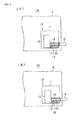
- Figs. 4(A) and 4(B) Modifications of the arrangement of the wireless IC device 30 in the first embodiment are shown in Figs. 4(A) and 4(B) .
- the conductor patterns 16 and 17 and a ground pattern 18 are formed on the power board 11 and the wireless IC device 30 is coupled to the conductor pattern 17 and the ground pattern 18.
- one conductor of the power cable 15 connected to the conductor pattern 17 functions as a monopole antenna.
- the wireless ICdevice 30 is coupled to the conductor patterns 16 and 17. In this case, both of the conductors of the power cable 15 connected to the conductor patterns 16 and 17 functioning as a dipole antenna.
- loop conductor 16a is not required in the first and second modifications described above, unlike the first embodiment, it is possible to reduce the area where the wireless IC device 30 is installed.
- a loop conductor 36 for impedance matching is formed on a child board 35 and the wireless ICdevice 30 is coupled to both ends of the loop conductor 36.
- the child board 35 is installed on the conductor pattern 16 formed on the power board 11 and, thus, the loop conductor 36 is coupled to the conductor pattern 16.
- the wireless IC device 30 is coupled to the loop conductor 36 and the loop conductor 36 is coupled to the power cable 15 via the conductor pattern 16. Accordingly, one of the conductors of the power cable 15 functions as a monopole antenna.
- the installation of the child board 35 on the power supply unit 10 allows even an electrical product on which the wireless IC device 30 is not planned to be installed to be incorporated in an RFID system.
- no power voltage or no external electrostatic input is directly applied to the wireless IC device 30 and, thus, it is possible to reduce the risk of breaking the wireless IC device 30.
- the wireless IC device 30 is installed on the power board 11, is (directly or indirectly) coupled to at least part of the power cable 15, and is connected to a main body control circuit 5 of the electrical product 1B.
- the conductor patterns 16 and 17 connected to the power cable 15 and a conductor pattern 20 connected to the main body control circuit 5 are formed on the power board 11, and the loop conductor 16a is formed in the conductor pattern 16.
- the wireless ICdevice 30 has a first terminal 31, a second terminal 32, and a third terminal 33.
- the first and second terminals 31 and 32 are coupled to the conductor pattern 16 (a bottom part of the loop conductor 16a).
- the third terminal 33 is coupled to an end of the conductor pattern 20.
- the conductor patterns 16 and 17 are connected to the power supply unit 12 (refer to Fig. 2 ).
- the first and second terminals 31 and 32 of the wireless IC device 30 are coupled to the loop conductor 16a to transmit power and a high-frequency signal
- the loop conductor 16a is coupled to one of the conductors of the power cable 15 via the conductor pattern 16, and the power cable 15 functions as a monopole antenna. Accordingly, it is possible to establish the communication between the wireless ICdevice 30 and the external reader-writer 50 via the power cable 15.
- the ground potential terminal is not limited to the above one.
- Another ground terminal may be additionally provided in the wireless IC device 30 and the terminal may be connected to the ground pattern on the board.
- necessary information is transmitted from the reader-writer 50 to the wireless IC device 30, for example, even when the electrical product main body 2 is turned off, the information is stored in the memory of the wireless IC device 30, and the information is transmitted from the wireless IC device 30 to the main body control circuit 5 when the main body 2 is turned on to allow a necessary instruction to be issued to the electrical product 1B.
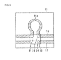
- the wireless IC device 30 is installed on the power board 11, the wireless IC device 30 is (directly or indirectly) coupled to at least part of the power cable 15, the wireless IC device 30 is connected to the main body control circuit 5 in the electrical product 1C, and power line communication with a server 55 is available via the power cable 15.
- the conductor patterns 16 and 17 connected to the power cable 15 are formed on the power board 11, and the loop conductor 16a is formed in the conductor pattern 16.
- the wireless IC device 30 has the first terminal 31, the second terminal 32, and the third terminal 33.
- the first and second terminals 31 and 32 are coupled to the conductor pattern 16 (a bottom part of the loop conductor 16a).
- the third terminal 33 is coupled to the conductor pattern 17.
- the conductor patterns 16 and 17 branch off into two to be connected to the power supply unit 12 (refer to Fig. 2 ) and the main body control circuit 5.
- the first and second terminals 31 and 32 of the wireless 1C device 30 are coupled to the loop conductor 16a to transmit power and a high-frequency signal
- the loop conductor 16a is coupled to one of the conductors of the power cable 15 via the conductor pattern 16, and the power cable 15 functions as a monopole antenna. Accordingly, it is possible to establish the communication between the wireless IC device 30 and the external reader-writer 50 via the power cable 15.
- the power line communication with the server 55 is available through the second and third terminals 32 and 33 of the wireless IC device 30 and via the power cable 15.
- the server 55 is capable of acquiring information about the electrical product 1C by the power line communication and transmitting information and/or an instruction to the wireless IC device 30.
- the communication of this type is available even when the electrical product 1C is turned off.
- the server 55 normally manages multiple electrical products.
- the power supply unit and the board thereof may have arbitrary configurations.
- the power cable may not be fixed to the power board side and may be detachably connected via a connector provided on the power board.
- An alternating current (AC) adopter may be configured as an external unit and the power board may receive direct current (DC).
- the present invention is useful for electrical products.
- the present invention is excellent in that the stable wireless communication is available and the wireless IC device can be prevented from, for example, being damaged or detached.
Landscapes
- Engineering & Computer Science (AREA)
- Computer Networks & Wireless Communication (AREA)
- Power Engineering (AREA)
- Signal Processing (AREA)
- Computer Hardware Design (AREA)
- Microelectronics & Electronic Packaging (AREA)
- Physics & Mathematics (AREA)
- General Physics & Mathematics (AREA)
- Theoretical Computer Science (AREA)
- Details Of Aerials (AREA)
- Near-Field Transmission Systems (AREA)
Abstract
To provide an electrical product capable of stable communication with a reader-writer and capable of preventing a wireless IC device from, for example, being damaged or detached.
A wireless IC device (30) processing a high-frequency signal is arranged in an electrical product main body (2), and an input-output terminal of the wireless IC device (30) is coupled to at least part of a power cable (15) externally extending from the electrical product main body (2).
Description
- The present invention relates to electrical products and, more particularly, to an electrical product capable of preferably using wireless communication including a radio frequency identification (RFID) system.
- Hitherto, RFID systems have been developed as article management systems. In such an RFID system, a reader-writer producing an electromagnetic field communicates with an RFID tag (wireless integrated circuit (IC) device) in a noncontact manner to transmit information. The RFID tag is attached to an article and stores certain information.
Patent Documents Patent Document 1, arrangement of a metal material around the tag can possibly inhibit stable communication with a reader writer. The mounting mode of the tag is not mentioned inPatent Document 2. - In contrast, Patent Document 3 discloses an example in which an RFID tag is attached on a power line or a plug and part of the power line is used as an antenna. However, when management is performed with the power cord being attached on a product, it is not possible to perform the management if the cord is pulled out from the product. It is not preferred to attach the tag on the cord in the light of repair or replacement of the cord when the cord is fixed to the product.
-
- Patent Document 1: Japanese Unexamined Patent Application Publication No.
2002-143826 - Patent Document 2: Japanese Unexamined Patent Application Publication No.
2003-308363 - Patent Document 3: Japanese Unexamined Patent Application Publication No.
2005-50581 - An object of the present invention is to provide an electrical product capable of stable communication with a reader-writer and capable of preventing its wireless IC device from, for example, being damaged or detached.
- In order to achieve the above object, an electrical product of an embodiment of the present invention is characterized in that a wireless IC device processing a high-frequency signal is arranged in a main body of the electrical product, and that an input-output terminal of the wireless IC device is coupled to at least part of a power cable externally extending from the main body of the electrical product.
- In the above electrical product, the power cable to which the wireless IC device is coupled functions as a monopole antenna or a dipole antenna to establish wireless communication with a reader-writer in order to manage, for example, the recycle and/or the life cycle of the electrical product. Since the power cable externally extending from the electrical product functions as an antenna, stable communication is available without causing a problem in the wireless communication even if a metal material is arranged adjacent to the wireless IC device or a cover of the electrical product is made of a metal. In addition, since the wireless IC device is arranged inside the main body of the electrical product, the wireless IC device is not damaged or detached due to, for example, an external impact.
- According to the present invention, it is possible to establish the stable wireless communication and to prevent the wireless ICdevice from, for example, being damaged or detached.
-
- [
Fig. 1] Fig. 1 is a descriptive diagram showing the relationship between an electrical product of a first embodiment and a communication system. - [
Fig. 2] Fig. 2 is a descriptive diagram showing an arrangement of a wireless IC device in the electrical product of the first embodiment. - [
Fig. 3] Fig. 3 is a descriptive diagram concerning a main part inFig. 2 . - [
Fig. 4] Figs. 4(A) and 4(B) descriptive diagrams showing other examples of the arrangement of the wireless IC device. - [
Fig. 5] Fig. 5 is a descriptive diagram showing another example of the wireless IC device. - [
Fig. 6] Fig. 6 is a descriptive diagram showing the relationship between an electrical product of a second embodiment and a communication system. - [
Fig. 7] Fig. 7 is a descriptive diagram showing an arrangement of a wireless IC device in the electrical product of the second embodiment. - [
Fig. 8] Fig. 8 is a descriptive diagram showing the relationship between an electrical product of a third embodiment and a communication system. - [
Fig. 9] Fig. 9 is a descriptive diagram showing an arrangement of a wireless IC device in the electrical product of the third embodiment. - Electrical products according to embodiments of the present invention will herein be described with reference to the attached drawings. The common reference numerals are used in each drawing to identify the same components and portions. A description of such components and portions is omitted herein,
- In an electrical product 1A of a first embodiment, as shown in
Fig. 1 , awireless 1C device 30 is installed on aboard 11 of apower supply unit 10 incorporated in a productmain body 2 made of, for example, a metal and thewireless ICdevice 30 is (directly or indirectly) coupled to at least part of apower cable 15 externally extending from the productmain body 2. Thepower cable 15 functions as an antenna for thewireless IC device 30 to perform wireless communication with a reader-writer 50 in an RFID system in a certain frequency band. The "coupling," in this description means any of direct electrical coupling, magnetic field coupling, electric field coupling, and electromagnetic field coupling. - Specifically, as shown in
Fig. 2 , thepower board 11 hasconductor patterns power supply unit 12. Theconductor patterns power cable 15. Aloop conductor 16a is formed in an intermediate part of theconductor pattern 16, as shown inFig. 3 . Input-output terminals wireless IC device 30 are coupled to both ends of theloop conductor 16a. Theloop conductor 16a has a function to match the impedance with thewireless IC device 30 in accordance with its line length. - The
wireless IC device 30 is heretofore commonly known as an RFID tag and includes a processing circuit (including a central processing unit (CPU) and a rewritable memory) processing a high-frequency signal. A combination of a wireless IC chip and a feed circuit board including a feed circuit coupled to the wireless IC chip may be used as thewireless IC device 30. - In the above configuration, the input-
output terminals wireless ICdevice 30 are coupled to theloop conductor 16a to transmit power and a high-frequency signal, theloop conductor 16a is coupled to one of the conductors of thepower cable 15 via theconductor pattern 16, and thepower cable 15 functions as a monopole antenna. Accordingly, it is possible to establish the communication between thewireless IC device 30 and the external reader-writer 50 via thepower cable 15. The communication is available even in a state in which thepower cable 15 is pulled out from an outlet. - Since the
power cable 15 externally extending from the electrical product 1A functions as an antenna in the first embodiment, stable communication is available without causing a problem in the wireless communication even if a metal material is arranged adjacent to thewireless IC device 30 or a cover of the electrical product is made of a metal. In addition, since thewireless IC device 30 is arranged inside the productmain body 2, thewireless IC device 30 is not damaged or detached due to, for example, an external impact. Furthermore, since thewireless IC device 30 is coupled to one conductor of thepower cable 15, the power voltage applied to the input-output terminals wireless IC device 30 is not damaged by the application of the voltage. - The
power board 11 may be a multilayer board and Theconductor patterns loop conductor 16a may be incorporated in theboard 11 when theboard 11 is formed of a multilayer board. Thewireless IC device 30 may be incorporated in theboard 11. - Modifications of the arrangement of the
wireless IC device 30 in the first embodiment are shown inFigs. 4(A) and 4(B) . In a first modification shown inFig. 4(A) , theconductor patterns ground pattern 18 are formed on thepower board 11 and thewireless IC device 30 is coupled to theconductor pattern 17 and theground pattern 18. In this case, one conductor of thepower cable 15 connected to theconductor pattern 17 functions as a monopole antenna. In a second modification shown inFig. 4(B) , thewireless ICdevice 30 is coupled to theconductor patterns power cable 15 connected to theconductor patterns - Since the
loop conductor 16a is not required in the first and second modifications described above, unlike the first embodiment, it is possible to reduce the area where thewireless IC device 30 is installed. - In a third modification shown in
Fig. 5 , aloop conductor 36 for impedance matching is formed on achild board 35 and thewireless ICdevice 30 is coupled to both ends of theloop conductor 36. Thechild board 35 is installed on theconductor pattern 16 formed on thepower board 11 and, thus, theloop conductor 36 is coupled to theconductor pattern 16. In other words, thewireless IC device 30 is coupled to theloop conductor 36 and theloop conductor 36 is coupled to thepower cable 15 via theconductor pattern 16. Accordingly, one of the conductors of thepower cable 15 functions as a monopole antenna. According to the third modification, the installation of thechild board 35 on thepower supply unit 10 allows even an electrical product on which thewireless IC device 30 is not planned to be installed to be incorporated in an RFID system. In addition, for example, no power voltage or no external electrostatic input is directly applied to thewireless IC device 30 and, thus, it is possible to reduce the risk of breaking thewireless IC device 30. - In an electrical product 1B of a second embodiment, as shown in
Fig. 6 , thewireless IC device 30 is installed on thepower board 11, is (directly or indirectly) coupled to at least part of thepower cable 15, and is connected to a mainbody control circuit 5 of the electrical product 1B. - Specifically, as shown in
Fig. 7 , theconductor patterns power cable 15 and aconductor pattern 20 connected to the mainbody control circuit 5 are formed on thepower board 11, and theloop conductor 16a is formed in theconductor pattern 16. Thewireless ICdevice 30 has afirst terminal 31, asecond terminal 32, and athird terminal 33. The first andsecond terminals loop conductor 16a). In addition, thethird terminal 33 is coupled to an end of theconductor pattern 20. Theconductor patterns Fig. 2 ). - In the above configuration, the first and
second terminals wireless IC device 30 are coupled to theloop conductor 16a to transmit power and a high-frequency signal, theloop conductor 16a is coupled to one of the conductors of thepower cable 15 via theconductor pattern 16, and thepower cable 15 functions as a monopole antenna. Accordingly, it is possible to establish the communication between the wireless ICdevice 30 and the external reader-writer 50 via thepower cable 15. In addition, it is possible to transmit necessary information to the mainbody control circuit 5 in a wired manner via the second andthird terminals wireless IC device 30. Although the terminal 32 and theconductor pattern 16 serve as terminals defining a ground potential for an information signal to be transmitted in the wired manner, the ground potential terminal is not limited to the above one. Another ground terminal may be additionally provided in thewireless IC device 30 and the terminal may be connected to the ground pattern on the board. - In the second embodiment, in addition to the functions of the above first embodiment, necessary information is transmitted from the reader-
writer 50 to thewireless IC device 30, for example, even when the electrical productmain body 2 is turned off, the information is stored in the memory of thewireless IC device 30, and the information is transmitted from thewireless IC device 30 to the mainbody control circuit 5 when themain body 2 is turned on to allow a necessary instruction to be issued to the electrical product 1B. - In an
electrical product 1C of a third embodiment, as shown inFig. 8 , thewireless IC device 30 is installed on thepower board 11, thewireless IC device 30 is (directly or indirectly) coupled to at least part of thepower cable 15, thewireless IC device 30 is connected to the mainbody control circuit 5 in theelectrical product 1C, and power line communication with aserver 55 is available via thepower cable 15. - Specifically, as shown in
Fig. 9 , theconductor patterns power cable 15 are formed on thepower board 11, and theloop conductor 16a is formed in theconductor pattern 16. Thewireless IC device 30 has thefirst terminal 31, thesecond terminal 32, and thethird terminal 33. The first andsecond terminals loop conductor 16a). In addition, thethird terminal 33 is coupled to theconductor pattern 17. Theconductor patterns Fig. 2 ) and the mainbody control circuit 5. - In the above configuration, the first and
second terminals wireless 1C deviceloop conductor 16a to transmit power and a high-frequency signal, theloop conductor 16a is coupled to one of the conductors of thepower cable 15 via theconductor pattern 16, and thepower cable 15 functions as a monopole antenna. Accordingly, it is possible to establish the communication between thewireless IC device 30 and the external reader-writer 50 via thepower cable 15. In addition, the power line communication with theserver 55 is available through the second andthird terminals wireless IC device 30 and via thepower cable 15. - In the third embodiment, in addition to the functions of the above first embodiment, for example, the
server 55 is capable of acquiring information about theelectrical product 1C by the power line communication and transmitting information and/or an instruction to thewireless IC device 30. The communication of this type is available even when theelectrical product 1C is turned off. Theserver 55 normally manages multiple electrical products. - The electrical products according to the present invention are not limited to the embodiments described above and it will be clear that various modifications can be made within the spirit and scope of the present invention.
- For example, electrical products, such as refrigerators, from which power cables are run are targeted and the present invention is widely applicable to various electrical products. The power supply unit and the board thereof may have arbitrary configurations. The power cable may not be fixed to the power board side and may be detachably connected via a connector provided on the power board. An alternating current (AC) adopter may be configured as an external unit and the power board may receive direct current (DC).
- As described above, the present invention is useful for electrical products. In particular, the present invention is excellent in that the stable wireless communication is available and the wireless IC device can be prevented from, for example, being damaged or detached.
-
- 1A, 1B, 1C electrical product
- 2 electrical product main body
- 5 main body control circuit
- 10 power supply unit
- 11 power board
- 15 power cable
- 16, 17, 20 conductor pattern
- 18 ground pattern
- 16a, 36 loop conductor
- 30 wireless IC device
- 31, 32, 33 input-output terminal
- 35 child board
- 50 reader-writer
- 55 server
Claims (8)
- An electrical product,
wherein a wireless IC device processing a high-frequency signal is arranged in a main body of the electrical product, and
wherein an input-output terminal of the wireless IC device is coupled to at least part of a power cable externally extending from the main body of the electrical product. - The electrical product according to Claim 1,
wherein the wireless IC device is installed on a surface or in a first board on which a power supply circuit is installed. - The electrical product according to Claim 2,
wherein a conductor pattern connected to the power cable is formed on the first board, and a loop conductor for impedance matching with the wireless IC device is formed in at least part of the conductor pattern, and
wherein the wireless IC device is coupled to the loop conductor. - The electrical product according to Claim 1,
wherein a loop conductor for impedance matching with the wireless IC device is formed on a second board, and
wherein the wireless IC device is coupled to the loop conductor and the loop conductor is coupled to at least part of the power cable. - The electrical product according to Claim 4,
wherein a conductor pattern connected to the power cable is formed on a first board on which a power supply circuit is installed, and
wherein the second board is installed on the first board and the loop conductor is coupled to the conductor pattern. - The electrical product according to any of Claims 1 to 5,
wherein the wireless IC device has a second input-output terminal other than a first input-output terminal directly or indirectly coupled to the power cable, and The second input-output terminal is connected to a control circuit of the main body of the electrical product via a communication wire. - The electrical product according to any of Claims 1 to 5,
wherein the wireless IC device has a second input-output terminal other than a first input-output terminal directly or indirectly coupled to the power cable, and the second input-output terminal functions as a terminal for power line communication via the power cable. - The electrical product according to any of Claims 1 to 7,
wherein the coupling between the wireless IC device and the power cable, the conductor pattern, or the loop conductor or the coupling between the loop conductor and the power cable or the conductor pattern is any of direct electrical coupling, magnetic field coupling, electric field coupling, and electromagnetic field coupling.
Applications Claiming Priority (2)
| Application Number | Priority Date | Filing Date | Title |
|---|---|---|---|
| JP2010268252 | 2010-12-01 | ||
| PCT/JP2011/074009 WO2012073608A1 (en) | 2010-12-01 | 2011-10-19 | Electrical appliance |
Publications (1)
| Publication Number | Publication Date |
|---|---|
| EP2592585A1 true EP2592585A1 (en) | 2013-05-15 |
Family
ID=46171560
Family Applications (1)
| Application Number | Title | Priority Date | Filing Date |
|---|---|---|---|
| EP11845261.4A Withdrawn EP2592585A1 (en) | 2010-12-01 | 2011-10-19 | Electrical appliance |
Country Status (5)
| Country | Link |
|---|---|
| US (1) | US20130140362A1 (en) |
| EP (1) | EP2592585A1 (en) |
| JP (1) | JP5387783B2 (en) |
| CN (1) | CN103026370A (en) |
| WO (1) | WO2012073608A1 (en) |
Family Cites Families (4)
| Publication number | Priority date | Publication date | Assignee | Title |
|---|---|---|---|---|
| US7135974B2 (en) * | 2002-04-22 | 2006-11-14 | Symbol Technologies, Inc. | Power source system for RF location/identification tags |
| JP2005050581A (en) * | 2003-07-30 | 2005-02-24 | Seiko Epson Corp | Power cord, power cord inspection device and power cord inspection method |
| JP4191088B2 (en) * | 2004-05-14 | 2008-12-03 | 株式会社デンソー | Electronic equipment |
| JP5104865B2 (en) * | 2007-07-18 | 2012-12-19 | 株式会社村田製作所 | Wireless IC device |
-
2011
- 2011-10-19 CN CN201180035339XA patent/CN103026370A/en active Pending
- 2011-10-19 JP JP2012546735A patent/JP5387783B2/en not_active Expired - Fee Related
- 2011-10-19 EP EP11845261.4A patent/EP2592585A1/en not_active Withdrawn
- 2011-10-19 WO PCT/JP2011/074009 patent/WO2012073608A1/en not_active Ceased
-
2013
- 2013-02-04 US US13/757,991 patent/US20130140362A1/en not_active Abandoned
Non-Patent Citations (1)
| Title |
|---|
| See references of WO2012073608A1 * |
Also Published As
| Publication number | Publication date |
|---|---|
| CN103026370A (en) | 2013-04-03 |
| US20130140362A1 (en) | 2013-06-06 |
| JP5387783B2 (en) | 2014-01-15 |
| JPWO2012073608A1 (en) | 2014-05-19 |
| WO2012073608A1 (en) | 2012-06-07 |
Similar Documents
| Publication | Publication Date | Title |
|---|---|---|
| CN111315613B (en) | Charging cable and adapter for charging a stored energy source at an energy supply device | |
| US8730121B2 (en) | Large scale folded dipole antenna for near-field RFID applications | |
| JP4482403B2 (en) | Non-contact information medium | |
| US5548282A (en) | Electronic shelf edge price display system | |
| CN104898532A (en) | Electrical activity sensor device for detecting electrical activity and electrical activity monitoring apparatus | |
| CN107911147B (en) | Control circuit for NFC near field communication and smart card | |
| US20140246504A1 (en) | Antenna device, card-type communication device, and communication terminal apparatus | |
| WO2014167881A1 (en) | Communication terminal | |
| CN101071906A (en) | Antenna apparatus and article management system | |
| JP4896922B2 (en) | Radio tag and conductive pipe having radio tag | |
| US8857723B2 (en) | Connection cable for the electrical or optical fiber connection of two system devices | |
| CN108698218B (en) | Hand-held power tool and amplifier antenna | |
| EP3549067A1 (en) | Systems and methods for improving performance of rfid tags | |
| US20160351994A1 (en) | Electrical activity sensor device for detecting electrical activity and electrical activity monitoring apparatus | |
| KR20120002207A (en) | Ubiquitous switchgear with smart remote control door | |
| CN105788975A (en) | Circuit breaker monitoring apparatus, circuit breaker and circuit breaker monitoring method | |
| CN107534219B (en) | Antenna device and electronic apparatus | |
| EP2592585A1 (en) | Electrical appliance | |
| EP1434159A3 (en) | Integrated antenna type non-contact IC card reader/writer | |
| US10528861B2 (en) | Radio-frequency identification transponder for aggressive environments | |
| CN209746555U (en) | Reader device and desk with reader device | |
| US20110070831A1 (en) | Coupler and communication system | |
| WO2022091443A1 (en) | Rfid communication system | |
| KR20180077599A (en) | Apparatus for transmitting power wirelessly | |
| US20160079716A1 (en) | Power socket apparatus with antenna module |
Legal Events
| Date | Code | Title | Description |
|---|---|---|---|
| PUAI | Public reference made under article 153(3) epc to a published international application that has entered the european phase |
Free format text: ORIGINAL CODE: 0009012 |
|
| 17P | Request for examination filed |
Effective date: 20130211 |
|
| AK | Designated contracting states |
Kind code of ref document: A1 Designated state(s): AL AT BE BG CH CY CZ DE DK EE ES FI FR GB GR HR HU IE IS IT LI LT LU LV MC MK MT NL NO PL PT RO RS SE SI SK SM TR |
|
| DAX | Request for extension of the european patent (deleted) | ||
| STAA | Information on the status of an ep patent application or granted ep patent |
Free format text: STATUS: THE APPLICATION HAS BEEN WITHDRAWN |
|
| 18W | Application withdrawn |
Effective date: 20150416 |