EP2590374A2 - Flexible receiver architecture - Google Patents
Flexible receiver architecture Download PDFInfo
- Publication number
- EP2590374A2 EP2590374A2 EP12188984.4A EP12188984A EP2590374A2 EP 2590374 A2 EP2590374 A2 EP 2590374A2 EP 12188984 A EP12188984 A EP 12188984A EP 2590374 A2 EP2590374 A2 EP 2590374A2
- Authority
- EP
- European Patent Office
- Prior art keywords
- circuit
- signal
- receiver
- signal path
- equalization
- Prior art date
- Legal status (The legal status is an assumption and is not a legal conclusion. Google has not performed a legal analysis and makes no representation as to the accuracy of the status listed.)
- Granted
Links
Images




Classifications
-
- H—ELECTRICITY
- H04—ELECTRIC COMMUNICATION TECHNIQUE
- H04L—TRANSMISSION OF DIGITAL INFORMATION, e.g. TELEGRAPHIC COMMUNICATION
- H04L25/00—Baseband systems
- H04L25/02—Details ; arrangements for supplying electrical power along data transmission lines
- H04L25/03—Shaping networks in transmitter or receiver, e.g. adaptive shaping networks
- H04L25/03006—Arrangements for removing intersymbol interference
- H04L25/03012—Arrangements for removing intersymbol interference operating in the time domain
- H04L25/03019—Arrangements for removing intersymbol interference operating in the time domain adaptive, i.e. capable of adjustment during data reception
- H04L25/03038—Arrangements for removing intersymbol interference operating in the time domain adaptive, i.e. capable of adjustment during data reception with a non-recursive structure
-
- H—ELECTRICITY
- H04—ELECTRIC COMMUNICATION TECHNIQUE
- H04L—TRANSMISSION OF DIGITAL INFORMATION, e.g. TELEGRAPHIC COMMUNICATION
- H04L25/00—Baseband systems
- H04L25/02—Details ; arrangements for supplying electrical power along data transmission lines
- H04L25/03—Shaping networks in transmitter or receiver, e.g. adaptive shaping networks
- H04L25/03006—Arrangements for removing intersymbol interference
- H04L25/03012—Arrangements for removing intersymbol interference operating in the time domain
- H04L25/03114—Arrangements for removing intersymbol interference operating in the time domain non-adaptive, i.e. not adjustable, manually adjustable, or adjustable only during the reception of special signals
- H04L25/03146—Arrangements for removing intersymbol interference operating in the time domain non-adaptive, i.e. not adjustable, manually adjustable, or adjustable only during the reception of special signals with a recursive structure
-
- H—ELECTRICITY
- H04—ELECTRIC COMMUNICATION TECHNIQUE
- H04L—TRANSMISSION OF DIGITAL INFORMATION, e.g. TELEGRAPHIC COMMUNICATION
- H04L25/00—Baseband systems
- H04L25/02—Details ; arrangements for supplying electrical power along data transmission lines
- H04L25/03—Shaping networks in transmitter or receiver, e.g. adaptive shaping networks
- H04L25/03006—Arrangements for removing intersymbol interference
- H04L2025/03433—Arrangements for removing intersymbol interference characterised by equaliser structure
- H04L2025/03535—Variable structures
- H04L2025/03547—Switching between time domain structures
- H04L2025/03566—Switching between time domain structures between different tapped delay line structures
- H04L2025/03573—Switching between time domain structures between different tapped delay line structures between recursive and non-recursive
Definitions
- the present invention relates generally to data communications. More particularly, the present invention relates to circuitry for high-speed data links.
- High-speed data links are used to communicate data between devices in a system.
- Serial interface protocols have been developed at increasingly fast data rates for such high-speed links. Examples of industry-standard protocols for serial interfaces include PCI Express ® (Peripheral Component Interconnect Express), XAUI (X Attachment Unit Interface), sRIO (serial Rapid IO), and others.
- equalization circuitry may be designed to implement a complex equalization technique, such circuitry typically consumes a large amount of power and is generally inflexible in terms of meeting the requirements of various different types of applications.
- the present invention is directed to a receiver circuit for a data link.
- the receiver circuit includes at least a first signal path, a second signal path, and a path selector circuit.
- the first signal path includes first equalization circuitry
- the second signal path includes second equalization circuitry.
- the path selector circuit is configured to select one signal path of the first and second signal paths.
- Another embodiment relates to an integrated circuit which includes at least a serial data receiver and a path selector circuit.
- the serial data circuit includes multiple signal paths, and each signal path includes at least one equalization circuit.
- the path selector circuit is configured to select one signal path of the multiple signal paths.
- the present invention is directed to a method of receiver equalization.
- a receiver circuit is configured to use a selected signal path of multiple signal paths for receiver equalization. Equalization may be performed on received data using the selected signal path while shutting off power to non-selected signal paths.
- the present disclosure provides an innovative receiver architecture that overcomes the above-discussed problems.
- the receiver architecture enables the flexible use of equalization circuitry which may be flexibly used with different types of applications.
- FIG. 1 is a high-level diagram of a communication link in accordance with an embodiment of the invention.
- a communication link is generally composed of a transmitter (TX) 120, a receiver (RX) 140, and a communication channel (CH) 130 that is located in between the transmitter and the receiver.
- TX transmitter
- RX receiver
- CH communication channel
- the TX 120 may include a parallel-in-serial-out (PISO) circuit 122.
- the PISO (serializer) circuit 122 is configured to receive parallel data signals and convert it to a serial data signal.
- the transmitter 120 may be part of an integrated circuit, and the parallel data signals may be provided by a communication protocol module in the integrated circuit.
- the serial data signal may be adjusted by a transmitter equalizer (TX EQ) circuit 124.
- TX EQ transmitter equalizer
- the TX EQ circuit124 may implement a finite impulse response (FIR) equalization that pre-distorts the transmitted signal to compensate for signal distortion in the channel 130.
- Clock generator (CLK) circuit 121 may utilize a phase locked loop circuit to provide a clock signal to the PISO 122 and TX EQ 124 circuits.
- the output from the TX EQ 124 circuit may be provided to a driver circuit 126.
- the driver circuit 126 may be configured to transmit the serial data signal over the channel 130.
- the channel 130 communicates the serial data signal from the transmitter 120 to the receiver 140.
- the channel 130 may use multiple lanes to communicate the serial data signal.
- the receiver 140 may be configured to receive the transmitted serial data signal from the multiple-lane channel into buffer circuitry 142.
- the buffer circuitry 142 may output the received serial data signal to receiver equalization (RX EQ) circuit 144.
- RX EQ circuit 144 may be configured to perform one or more equalizations, as described further herein, to compensate for high-frequency signal loss in the channel.
- the RX EQ circuit 144 may output an "equalized" serial data signal to both a clock data recovery (CDR) circuit 145 and to a data input of a latch circuit 146.
- CDR clock data recovery
- the CDR circuit 145 may use a PLL to recover the clock signal from the serial data signal.
- the recovered clock signal may be provided to clock inputs of the RX EQ circuit 144 and to a latch circuit 146.
- the latch circuit 146 may be configured to receive the "equalized" serial data signal from the RX EQ circuit 144 at its data input and to receive the recovered clock signal from the CDR circuit 145 at its clock input.
- the latch circuit 146 outputs the regenerated serial data signal to a serial-in-parallel-out (SIPO) circuit 148.
- the SIPO (serializer) circuit 148 is configured to receive a serial data signal and convert it to parallel data signals.
- the parallel data signals may be provided to other circuitry of the receiving device.
- the receiving device may be an integrated circuit, and the parallel data signals may be provided to a communication protocol module in the integrated circuit.
- FIG. 2 depicts a receiver equalizer (RX EQ) circuit 144 in accordance with an embodiment of the invention.
- the RX EQ circuit 144 receives a serial data signal from the RX buffer circuit 142, and, after applying equalization to the serial data signal, outputs the "equalized" serial data signal to the CDR circuit 145 and the latch circuit 146.
- the serial data signal from the RX buffer circuit 142 is received by a first continuous-time linear estimation (CTLE) circuit 202.
- the first CTLE circuit 202 applies an initial, generally linear, compensation to the signal.
- One embodiment of the first CTLE circuit 202 is described below in relation to FIG. 3 .
- the first CTLE circuit 202 may provide its output signal to two signal paths.
- a first signal path is shown on the bottom in the figure and may lead to a second CTLE circuit 204.
- the second CTLE circuit 204 applies a further, generally linear, compensation to the signal.
- the second CTLE circuit 204 may also be implemented as described below in relation to FIG. 3 .
- the second CTLE circuit 204 may provide its output signal to a decision feedback equalizer (DFE) circuit 206.
- the DFE circuit 206 is a non-linear equalization circuit which uses feedback relating to the logic state of previously-transmitted data bits in order to decide the logic state of a present data bit.
- Various embodiments of a DFE circuit 206 may be utilized.
- the DFE circuit 206 may be implemented as described in U.S. Patent No.
- the DFE circuit 206 may be implemented in a similar way as disclosed in " A 20Gb/s 40mW Equalizer in 90nm CMOS Technology," by Sameh A. (2004) and Behzad Razavi, Digest of Technical Papers, IEEE International Solid-State Circuits Conference (ISSCC), February 2010, pp. 170-171 .
- the DFE circuit 206 may be implemented with other conventional designs.
- the second signal path is shown on the top in the figure and may include one or more analog equalizer circuits in series. As depicted in FIG. 2 , the second signal path includes a series of N CTLE circuits (208-1 through 208-N), where N is at least one. In one embodiment, each CTLE circuit 208-n may be a variable CTLE circuit. One embodiment of a variable CTLE circuit is described below in relation to FIG. 4 . Other embodiments may also include variable CTLE circuits and non-variable CTLE circuits (for example, as shown in FIG. 3 ) in the series.
- the output of the DFE circuit 206 of the first signal path may be provided to a first input (1) of a path selector circuit 210, and the output of the last CTLE circuit 208-N of the second signal path may be provided to a second input (0) of the path selector circuit 210.
- the path selector circuit 210 may be configured to select the "equalized" serial data signal from either the first input or the second input.
- One embodiment of the path selector circuit 210 is described below in relation to FIG. 5 .
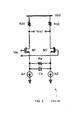
- FIG. 3 depicts a CTLE circuit 300 in accordance with an embodiment of the invention.
- the CTLE circuit 300 may include two drain resistors Rd1 and Rd2, transistors M1 and M2, source resistor Rs, source capacitor Cs, and two source current sinks Is1 and Is2.
- the drain resistor Rd1 may be connected between the drain of transistor M1 and voltage source Vdd
- the drain resistor Rd2 may be connected between the drain of transistor M2 and voltage source Vdd.
- the current sink Is1 may be connected between the source of transistor M1 and ground
- the current sink Is2 may be connected between the source of transistor M2 and ground.
- the differential input signal Vin is provided to the gates of the transistors M1 and M2, and the differential output signal Vout is generated at two output nodes, where a first output node is between the drain of transistor M1 and drain resistor Rd1, and a second output node is between the drain of transistor M2 and the drain resistor Rd2.
- the source capacitor Cs and the source resistor Rs may be connected in a parallel manner between the sources of the two transistors M1 and M2.
- the source capacitor Cs functions as a peaking capacitor that may be used to adjust the amount of gain produced at the resonant frequency.
- the source resistor Rs functions as a source degeneration resistor that may be used to adjust a low-frequency gain of the CTLE circuit 300.
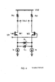
- FIG. 4 depicts a variable CTLE circuit 400 in accordance with an embodiment of the invention.
- the variable CTLE circuit 400 of FIG. 4 is similar to the CTLE circuit 300vof FIG. 3 .
- the differences are that, in the variable CTLE circuit 400, the source capacitor is a variable capacitor Cv, and the source resistor is a variable resistor Rv.
- the variable capacitor Cv and variable resistor Rv enable the adjustment of the frequency and gain characteristics of the circuit 400 for equalization purposes.
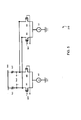
- FIG. 5 depicts a path selector circuit 210 in accordance with an embodiment of the invention.
- the path selector circuit 210 may include two resistors Rd1 and Rd2, a first pair of transistors M1 and M2, a second pair of transistors M3 and M4, and two current sinks Is0 and Is1.
- the resistor Rd1 may be connected between the voltage source Vdd and the drain of transistor M1 and also between the voltage source Vdd and the drain of transistor M3.
- the resistor Rd2 may be connected between the voltage source Vdd and the drain of transistor M2 and also between the voltage source Vdd and the drain of transistor M4.
- the current sink Is0 may be connected between the source of transistor M1 and ground and also between the source of transistor M2 and ground.
- the current sink Is1 may be connected between the source of transistor M3 and ground and also between the source of transistor M4 and ground.
- a first differential input signal Vin0 may be provided to the gates of the first pair of transistors M1 and M2, and a second differential input signal Vin1 may be provided to the gates of the second pair of transistors M3 and M4.
- the differential output signal Vout is generated at two output nodes.
- a first output node is between the resistor Rd1 and the drain of transistor M1 and also between the resistor Rd1 and the drain of transistor M3.
- a second output node is between the resistor Rd2 and the drain of transistor M2 and also between the resistor Rd2 and the drain of transistor M4.
- the first current sink Is0 is turned on, while the second current sink Is1 is turned off.
- the second current sink Is1 is turned on, while the first current sink Is0 is turned off.
- FIG. 6 is a flow chart of a method 600 for receiver equalization in accordance with an embodiment of the invention.
- An integrated circuit with a multiple-path receiver equalizer is provided 602.
- the multiple path receiver may have two signal paths, as described above in relation to FIG. 2 .
- the integrated circuit may then be configured (programmed) 604 to utilize a selected signal path for receiver equalization. Equalization may then be performed 606 on received data using the selected signal path while turning off power to the non-selected signal path(s).
- selection of the first path on the bottom of FIG. 2 may be advantageous in certain applications due to the capabilities of the DFE circuit 206 to reduce inter-symbol interference (ISI) while being less sensitive to clock jitter.
- ISI inter-symbol interference
- the DFE circuit 206 generally requires a relatively large amount of power to operate.
- selection of the second path on the top of FIG. 2 may be sufficient in certain applications and may advantageously consume less power than the first path.
- the consumption of less power is achieved by deactivating (turning off power to) the circuitry of the first path.
- the present disclosure provides a flexible architecture for receiver equalization which may be advantageously configured depending on the link application.
- the first path including the DFE may be selected.
- the second path (the series of CTLE) may be selected so as to conserve a substantial amount of power.
- the circuitry of the second path may be configured to support a wide-bandwidth with no AC boost.
- the second path may also be selected to support lower-speed 10-16 Gbps applications.
- the circuitry of the second path may be configured to boost a signal amplitude at lower frequencies (i.e. provide an AC boost at the lower frequencies).
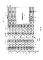
- FIG. 7 is a simplified partial block diagram of a field programmable gate array (FPGA) 10 that can include aspects of the present invention. It should be understood that embodiments of the present invention can be used in numerous types of integrated circuits such as field programmable gate arrays (FPGAs), programmable logic devices (PLDs), complex programmable logic devices (CPLDs), programmable logic arrays (PLAs), digital signal processors (DSPs) and application specific integrated circuits (ASICs).
- FPGAs field programmable gate arrays
- PLDs programmable logic devices
- CPLDs complex programmable logic devices
- PLAs programmable logic arrays
- DSPs digital signal processors
- ASICs application specific integrated circuits
- FPGA 10 includes within its "core" a two-dimensional array of programmable logic array blocks (or LABs) 12 that are interconnected by a network of column and row interconnect conductors of varying length and speed.
- LABs 12 include multiple (e.g., ten) logic elements (or LEs).
- An LE is a programmable logic block that provides for efficient implementation of user defined logic functions.
- An FPGA has numerous logic elements that can be configured to implement various combinatorial and sequential functions.
- the logic elements have access to a programmable interconnect structure.
- the programmable interconnect structure can be programmed to interconnect the logic elements in almost any desired configuration.
- FPGA 10 may also include a distributed memory structure including random access memory (RAM) blocks of varying sizes provided throughout the array.
- RAM random access memory
- the RAM blocks include, for example, blocks 14, blocks 16, and block 18. These memory blocks can also include shift registers and FIFO buffers.
- FPGA 10 may further include digital signal processing (DSP) blocks 20 that can implement, for example, multipliers with add or subtract features.
- DSP digital signal processing
- IOEs Input/output elements 22 located, in this example, around the periphery of the chip support numerous single-ended and differential input/output standards. Each IOE 22 is coupled to an external terminal (i.e., a pin) of FPGA 10.
- a transceiver (TX/RX) channel array may be arranged as shown, for example, with each TX/RX channel circuit 30 being coupled to several LABs.
- a TX/RX channel circuit 30 may include, among other circuitry, the receiver circuitry described herein.
- FPGA 10 is described herein for illustrative purposes only and that the present invention can be implemented in many different types of PLDs, FPGAs, and ASICs.
- FIG. 8 shows a block diagram of an exemplary digital system 50 that can embody techniques of the present invention.
- System 50 may be a programmed digital computer system, digital signal processing system, specialized digital switching network, or other processing system. Moreover, such systems can be designed for a wide variety of applications such as telecommunications systems, automotive systems, control systems, consumer electronics, personal computers, Internet communications and networking, and others. Further, system 50 may be provided on a single board, on multiple boards, or within multiple enclosures.
- System 50 includes a processing unit 52, a memory unit 54, and an input/output (I/O) unit 56 interconnected together by one or more buses.
- FPGA 58 is embedded in processing unit 52.
- FPGA 58 can serve many different purposes within the system 50.
- FPGA 58 can, for example, be a logical building block of processing unit 52, supporting its internal and external operations.
- FPGA 58 is programmed to implement the logical functions necessary to carry on its particular role in system operation.
- FPGA 58 can be specially coupled to memory 54 through connection 60 and to I/O unit 56 through connection 62.
- Processing unit 52 may direct data to an appropriate system component for processing or storage, execute a program stored in memory 54, receive and transmit data via I/O unit 56, or other similar function.
- Processing unit 52 may be a central processing unit (CPU), microprocessor, floating point coprocessor, graphics coprocessor, hardware controller, microcontroller, field programmable gate array programmed for use as a controller, network controller, or any type of processor or controller. Furthermore, in many embodiments, there is often no need for a CPU.
- FPGA 58 may control the logical operations of the system.
- FPGA 58 acts as a reconfigurable processor that may be reprogrammed as needed to handle a particular computing task.
- FPGA 58 may itself include an embedded microprocessor.
- Memory unit 54 may be a random access memory (RAM), read only memory (ROM), fixed or flexible disk media, flash memory, tape, or any other storage means, or any combination of these storage means.
Landscapes
- Engineering & Computer Science (AREA)
- Power Engineering (AREA)
- Computer Networks & Wireless Communication (AREA)
- Signal Processing (AREA)
- Dc Digital Transmission (AREA)
- Detection And Prevention Of Errors In Transmission (AREA)
- Cable Transmission Systems, Equalization Of Radio And Reduction Of Echo (AREA)
- Circuits Of Receivers In General (AREA)
Abstract
Description
- The present invention relates generally to data communications. More particularly, the present invention relates to circuitry for high-speed data links.
- High-speed data links are used to communicate data between devices in a system. Serial interface protocols have been developed at increasingly fast data rates for such high-speed links. Examples of industry-standard protocols for serial interfaces include PCI Express® (Peripheral Component Interconnect Express), XAUI (X Attachment Unit Interface), sRIO (serial Rapid IO), and others.
- As the operating speed of the high-speed data links increases to rates which are tens of gigabits per second (Gbps), sophisticated equalization schemes become more necessary to compensate for high-frequency signal loss. Unfortunately, while equalization circuitry may be designed to implement a complex equalization technique, such circuitry typically consumes a large amount of power and is generally inflexible in terms of meeting the requirements of various different types of applications.
- The invention is defined in
claims 1 and 13, respectively. - In one aspect, the present invention is directed to a receiver circuit for a data link. The receiver circuit includes at least a first signal path, a second signal path, and a path selector circuit. The first signal path includes first equalization circuitry, and the second signal path includes second equalization circuitry. The path selector circuit is configured to select one signal path of the first and second signal paths.
- Another embodiment relates to an integrated circuit which includes at least a serial data receiver and a path selector circuit. The serial data circuit includes multiple signal paths, and each signal path includes at least one equalization circuit. The path selector circuit is configured to select one signal path of the multiple signal paths.
- In another aspect, the present invention is directed to a method of receiver equalization. A receiver circuit is configured to use a selected signal path of multiple signal paths for receiver equalization. Equalization may be performed on received data using the selected signal path while shutting off power to non-selected signal paths.
- Other embodiments and features are also disclosed.
-
-
FIG. 1 is a high-level diagram of a communication link in accordance with an embodiment of the invention. -
FIG. 2 depicts a receiver equalizer circuit in accordance with an embodiment of the invention. -
FIG. 3 depicts a continuous-time linear estimation (CTLE) circuit in accordance with an embodiment of the invention. -
FIG. 4 depicts a variable CTLE circuit in accordance with an embodiment of the invention. -
FIG. 5 depicts a path selector circuit in accordance with an embodiment of the invention. -
FIG. 6 is a flow chart of a method for receiving a serial data signal in accordance with an embodiment of the invention. -
FIG. 7 is a simplified partial block diagram of a field programmable gate array (FPGA) that can include aspects of the present invention. -
FIG. 8 is a block diagram of an exemplary digital system that can employ techniques of the present invention. - The present disclosure provides an innovative receiver architecture that overcomes the above-discussed problems. The receiver architecture enables the flexible use of equalization circuitry which may be flexibly used with different types of applications.
-
FIG. 1 is a high-level diagram of a communication link in accordance with an embodiment of the invention. As shown inFIG. 1 , a communication link is generally composed of a transmitter (TX) 120, a receiver (RX) 140, and a communication channel (CH) 130 that is located in between the transmitter and the receiver.. - The TX 120 may include a parallel-in-serial-out (PISO)
circuit 122. The PISO (serializer)circuit 122 is configured to receive parallel data signals and convert it to a serial data signal. For example, thetransmitter 120 may be part of an integrated circuit, and the parallel data signals may be provided by a communication protocol module in the integrated circuit. - The serial data signal may be adjusted by a transmitter equalizer (TX EQ)
circuit 124. In one embodiment, the TX EQ circuit124 may implement a finite impulse response (FIR) equalization that pre-distorts the transmitted signal to compensate for signal distortion in thechannel 130. Clock generator (CLK)circuit 121 may utilize a phase locked loop circuit to provide a clock signal to thePISO 122 and TXEQ 124 circuits. The output from the TX EQ 124 circuit may be provided to adriver circuit 126. Thedriver circuit 126 may be configured to transmit the serial data signal over thechannel 130. - The
channel 130 communicates the serial data signal from thetransmitter 120 to thereceiver 140. Thechannel 130 may use multiple lanes to communicate the serial data signal. - The
receiver 140 may be configured to receive the transmitted serial data signal from the multiple-lane channel intobuffer circuitry 142. Thebuffer circuitry 142 may output the received serial data signal to receiver equalization (RX EQ)circuit 144. TheRX EQ circuit 144 may be configured to perform one or more equalizations, as described further herein, to compensate for high-frequency signal loss in the channel. TheRX EQ circuit 144 may output an "equalized" serial data signal to both a clock data recovery (CDR)circuit 145 and to a data input of alatch circuit 146. - The
CDR circuit 145 may use a PLL to recover the clock signal from the serial data signal. The recovered clock signal may be provided to clock inputs of theRX EQ circuit 144 and to alatch circuit 146. - The
latch circuit 146 may be configured to receive the "equalized" serial data signal from theRX EQ circuit 144 at its data input and to receive the recovered clock signal from theCDR circuit 145 at its clock input. Thelatch circuit 146 outputs the regenerated serial data signal to a serial-in-parallel-out (SIPO)circuit 148. The SIPO (serializer)circuit 148 is configured to receive a serial data signal and convert it to parallel data signals. The parallel data signals may be provided to other circuitry of the receiving device. For example, the receiving device may be an integrated circuit, and the parallel data signals may be provided to a communication protocol module in the integrated circuit. -
FIG. 2 depicts a receiver equalizer (RX EQ)circuit 144 in accordance with an embodiment of the invention. As shown, theRX EQ circuit 144 receives a serial data signal from theRX buffer circuit 142, and, after applying equalization to the serial data signal, outputs the "equalized" serial data signal to theCDR circuit 145 and thelatch circuit 146. - The serial data signal from the
RX buffer circuit 142 is received by a first continuous-time linear estimation (CTLE)circuit 202. Thefirst CTLE circuit 202 applies an initial, generally linear, compensation to the signal. One embodiment of thefirst CTLE circuit 202 is described below in relation toFIG. 3 . Thefirst CTLE circuit 202 may provide its output signal to two signal paths. - A first signal path is shown on the bottom in the figure and may lead to a
second CTLE circuit 204. Thesecond CTLE circuit 204 applies a further, generally linear, compensation to the signal. In one embodiment, thesecond CTLE circuit 204 may also be implemented as described below in relation toFIG. 3 . Thesecond CTLE circuit 204 may provide its output signal to a decision feedback equalizer (DFE)circuit 206. TheDFE circuit 206 is a non-linear equalization circuit which uses feedback relating to the logic state of previously-transmitted data bits in order to decide the logic state of a present data bit. Various embodiments of aDFE circuit 206 may be utilized. For example, in one embodiment, theDFE circuit 206 may be implemented as described inU.S. Patent No. 7,697,603, issued April 13, 2010 to Wang et al. , the disclosure of which is hereby incorporated by reference in its entirety. In another embodiment, theDFE circuit 206 may be implemented in a similar way as disclosed in "A 20Gb/s 40mW Equalizer in 90nm CMOS Technology," by Sameh A. Ibrahim and Behzad Razavi, Digest of Technical Papers, IEEE International Solid-State Circuits Conference (ISSCC), February 2010, pp. 170-171. In other embodiments, theDFE circuit 206 may be implemented with other conventional designs. - The second signal path is shown on the top in the figure and may include one or more analog equalizer circuits in series. As depicted in
FIG. 2 , the second signal path includes a series of N CTLE circuits (208-1 through 208-N), where N is at least one. In one embodiment, each CTLE circuit 208-n may be a variable CTLE circuit. One embodiment of a variable CTLE circuit is described below in relation toFIG. 4 . Other embodiments may also include variable CTLE circuits and non-variable CTLE circuits (for example, as shown inFIG. 3 ) in the series. - The output of the
DFE circuit 206 of the first signal path may be provided to a first input (1) of apath selector circuit 210, and the output of the last CTLE circuit 208-N of the second signal path may be provided to a second input (0) of thepath selector circuit 210. Thepath selector circuit 210 may be configured to select the "equalized" serial data signal from either the first input or the second input. One embodiment of thepath selector circuit 210 is described below in relation toFIG. 5 . -
FIG. 3 depicts aCTLE circuit 300 in accordance with an embodiment of the invention. As depicted, theCTLE circuit 300 may include two drain resistors Rd1 and Rd2, transistors M1 and M2, source resistor Rs, source capacitor Cs, and two source current sinks Is1 and Is2. The drain resistor Rd1 may be connected between the drain of transistor M1 and voltage source Vdd, and the drain resistor Rd2 may be connected between the drain of transistor M2 and voltage source Vdd. The current sink Is1 may be connected between the source of transistor M1 and ground, and the current sink Is2 may be connected between the source of transistor M2 and ground. - The differential input signal Vin is provided to the gates of the transistors M1 and M2, and the differential output signal Vout is generated at two output nodes, where a first output node is between the drain of transistor M1 and drain resistor Rd1, and a second output node is between the drain of transistor M2 and the drain resistor Rd2. The source capacitor Cs and the source resistor Rs may be connected in a parallel manner between the sources of the two transistors M1 and M2. The source capacitor Cs functions as a peaking capacitor that may be used to adjust the amount of gain produced at the resonant frequency. The source resistor Rs functions as a source degeneration resistor that may be used to adjust a low-frequency gain of the
CTLE circuit 300. -
FIG. 4 depicts avariable CTLE circuit 400 in accordance with an embodiment of the invention. Thevariable CTLE circuit 400 ofFIG. 4 is similar to the CTLE circuit 300vofFIG. 3 . The differences are that, in thevariable CTLE circuit 400, the source capacitor is a variable capacitor Cv, and the source resistor is a variable resistor Rv. The variable capacitor Cv and variable resistor Rv enable the adjustment of the frequency and gain characteristics of thecircuit 400 for equalization purposes. -
FIG. 5 depicts apath selector circuit 210 in accordance with an embodiment of the invention. As depicted, thepath selector circuit 210 may include two resistors Rd1 and Rd2, a first pair of transistors M1 and M2, a second pair of transistors M3 and M4, and two current sinks Is0 and Is1. The resistor Rd1 may be connected between the voltage source Vdd and the drain of transistor M1 and also between the voltage source Vdd and the drain of transistor M3. The resistor Rd2 may be connected between the voltage source Vdd and the drain of transistor M2 and also between the voltage source Vdd and the drain of transistor M4. The current sink Is0 may be connected between the source of transistor M1 and ground and also between the source of transistor M2 and ground. The current sink Is1 may be connected between the source of transistor M3 and ground and also between the source of transistor M4 and ground. - A first differential input signal Vin0 may be provided to the gates of the first pair of transistors M1 and M2, and a second differential input signal Vin1 may be provided to the gates of the second pair of transistors M3 and M4. The differential output signal Vout is generated at two output nodes. A first output node is between the resistor Rd1 and the drain of transistor M1 and also between the resistor Rd1 and the drain of transistor M3. A second output node is between the resistor Rd2 and the drain of transistor M2 and also between the resistor Rd2 and the drain of transistor M4.
- To select the first differential input signal Vin0 to drive the output signal Vout, the first current sink Is0 is turned on, while the second current sink Is1 is turned off. To select the second differential input signal Vin1 to drive the output signal Vout, the second current sink Is1 is turned on, while the first current sink Is0 is turned off.
-
FIG. 6 is a flow chart of amethod 600 for receiver equalization in accordance with an embodiment of the invention. An integrated circuit with a multiple-path receiver equalizer is provided 602. In one embodiment, the multiple path receiver may have two signal paths, as described above in relation toFIG. 2 . The integrated circuit may then be configured (programmed) 604 to utilize a selected signal path for receiver equalization. Equalization may then be performed 606 on received data using the selected signal path while turning off power to the non-selected signal path(s). - Referring to the equalization circuitry 200 described above in relation to
FIG. 2 , selection of the first path on the bottom ofFIG. 2 (withCTLE 204 and DFE 206) may be advantageous in certain applications due to the capabilities of theDFE circuit 206 to reduce inter-symbol interference (ISI) while being less sensitive to clock jitter. However, theDFE circuit 206 generally requires a relatively large amount of power to operate. - On the other hand, selection of the second path on the top of
FIG. 2 (with the series of CTLE circuits 208-1 through 208-N) may be sufficient in certain applications and may advantageously consume less power than the first path. The consumption of less power is achieved by deactivating (turning off power to) the circuitry of the first path. - Thus, the present disclosure provides a flexible architecture for receiver equalization which may be advantageously configured depending on the link application. For example, to support longer-range applications, such as 25 to 28 Gbps backplane applications, the first path (including the DFE) may be selected.
- On the other hand, to support shorter-range applications, such as 28 Gbps chip-to-chip applications, the second path (the series of CTLE) may be selected so as to conserve a substantial amount of power. In this case, the circuitry of the second path may be configured to support a wide-bandwidth with no AC boost.
- The second path may also be selected to support lower-speed 10-16 Gbps applications. In this case, the circuitry of the second path may be configured to boost a signal amplitude at lower frequencies (i.e. provide an AC boost at the lower frequencies).
-
FIG. 7 is a simplified partial block diagram of a field programmable gate array (FPGA) 10 that can include aspects of the present invention. It should be understood that embodiments of the present invention can be used in numerous types of integrated circuits such as field programmable gate arrays (FPGAs), programmable logic devices (PLDs), complex programmable logic devices (CPLDs), programmable logic arrays (PLAs), digital signal processors (DSPs) and application specific integrated circuits (ASICs). -
FPGA 10 includes within its "core" a two-dimensional array of programmable logic array blocks (or LABs) 12 that are interconnected by a network of column and row interconnect conductors of varying length and speed.LABs 12 include multiple (e.g., ten) logic elements (or LEs). - An LE is a programmable logic block that provides for efficient implementation of user defined logic functions. An FPGA has numerous logic elements that can be configured to implement various combinatorial and sequential functions. The logic elements have access to a programmable interconnect structure. The programmable interconnect structure can be programmed to interconnect the logic elements in almost any desired configuration.
-
FPGA 10 may also include a distributed memory structure including random access memory (RAM) blocks of varying sizes provided throughout the array. The RAM blocks include, for example, blocks 14, blocks 16, and block 18. These memory blocks can also include shift registers and FIFO buffers. -
FPGA 10 may further include digital signal processing (DSP) blocks 20 that can implement, for example, multipliers with add or subtract features. Input/output elements (IOEs) 22 located, in this example, around the periphery of the chip support numerous single-ended and differential input/output standards. EachIOE 22 is coupled to an external terminal (i.e., a pin) ofFPGA 10. A transceiver (TX/RX) channel array may be arranged as shown, for example, with each TX/RX channel circuit 30 being coupled to several LABs. A TX/RX channel circuit 30 may include, among other circuitry, the receiver circuitry described herein. - It is to be understood that
FPGA 10 is described herein for illustrative purposes only and that the present invention can be implemented in many different types of PLDs, FPGAs, and ASICs. - The present invention can also be implemented in a system that has a FPGA as one of several components.
FIG. 8 shows a block diagram of an exemplarydigital system 50 that can embody techniques of the present invention.System 50 may be a programmed digital computer system, digital signal processing system, specialized digital switching network, or other processing system. Moreover, such systems can be designed for a wide variety of applications such as telecommunications systems, automotive systems, control systems, consumer electronics, personal computers, Internet communications and networking, and others. Further,system 50 may be provided on a single board, on multiple boards, or within multiple enclosures. -
System 50 includes aprocessing unit 52, amemory unit 54, and an input/output (I/O)unit 56 interconnected together by one or more buses. According to this exemplary embodiment,FPGA 58 is embedded inprocessing unit 52.FPGA 58 can serve many different purposes within thesystem 50.FPGA 58 can, for example, be a logical building block ofprocessing unit 52, supporting its internal and external operations.FPGA 58 is programmed to implement the logical functions necessary to carry on its particular role in system operation.FPGA 58 can be specially coupled tomemory 54 throughconnection 60 and to I/O unit 56 throughconnection 62. - Processing
unit 52 may direct data to an appropriate system component for processing or storage, execute a program stored inmemory 54, receive and transmit data via I/O unit 56, or other similar function. Processingunit 52 may be a central processing unit (CPU), microprocessor, floating point coprocessor, graphics coprocessor, hardware controller, microcontroller, field programmable gate array programmed for use as a controller, network controller, or any type of processor or controller. Furthermore, in many embodiments, there is often no need for a CPU. - For example, instead of a CPU, one or
more FPGAs 58 may control the logical operations of the system. As another example,FPGA 58 acts as a reconfigurable processor that may be reprogrammed as needed to handle a particular computing task. Alternately,FPGA 58 may itself include an embedded microprocessor.Memory unit 54 may be a random access memory (RAM), read only memory (ROM), fixed or flexible disk media, flash memory, tape, or any other storage means, or any combination of these storage means. - In the above description, numerous specific details are given to provide a thorough understanding of embodiments of the invention. However, the above description of illustrated embodiments of the invention is not intended to be exhaustive or to limit the invention to the precise forms disclosed. One skilled in the relevant art will recognize that the invention can be practiced without one or more of the specific details, or with other methods, components, etc.
- In other instances, well-known structures or operations are not shown or described in detail to avoid obscuring aspects of the invention. While specific embodiments of, and examples for, the invention are described herein for illustrative purposes, various equivalent modifications are possible within the scope of the invention, as those skilled in the relevant art will recognize. These modifications may be made to the invention in light of the above detailed description.
Claims (16)
- A receiver circuit for a data link, the receiver circuit comprising:a first signal path including first equalization circuitry;a second signal path including second equalization circuitry; anda path selector circuit which is configured to select one signal path of the first and second signal paths.
- The receiver circuit of claim 1, wherein the first signal path comprises a decision feedback equalizer circuit.
- The receiver circuit of claim 2, wherein the first signal path comprises a continuous-time linear estimation circuit in series with the decision feedback equalizer circuit.
- The receiver circuit of any of claims 1-3, wherein the second signal path comprises at least one analog equalizer circuit.
- The receiver circuit of claim 4, wherein the second signal path comprises a variable continuous-time linear estimation circuit.
- The receiver circuit of claim 5, wherein the variable continuous-time linear estimation circuit is configured to boost a signal amplitude for a range of frequencies.
- The receiver circuit of claim 4, wherein the second signal path comprises a series of continuous-time linear estimation circuits, including at least one variable continuous-time linear estimation circuit.
- The receiver circuit of any of claims 1-7, wherein the receiver circuit is configured to shut-off power to an un-selected signal path.
- The receiver circuit of any of claims 1-8, further comprising:a first analog equalizer circuit for receiving a data signal and for outputting the data signal to the first and second signal paths.
- The receiver circuit of claim 9, further comprising:a buffer circuit for providing the data signal to the first analog equalizer circuit; anda clock data recovery circuit for receiving an equalized data signal from the path selector circuit.
- The receiver circuit of any of the preceding claims, wherein the receiver circuit is an integrated circuit.
- The receiver circuit of claim 11, wherein the integrated circuit comprises a field programmable gate array.
- A method of receiver equalization, the method comprising:configuring a receiver circuit with a multiple-path receiver equalizer to use a selected signal path for receiver equalization; andperforming equalization on received data using the selected signal path.
- The method of claim 13, wherein a first signal path comprises a decision feedback equalization circuit.
- The method of claim 14, further comprising:shutting off power to the decision feedback equalization circuit if the first signal path is not selected.
- The method of claim 14 or 15, wherein a second signal path comprises a variable continuous-time linear estimation circuit.
Applications Claiming Priority (1)
| Application Number | Priority Date | Filing Date | Title |
|---|---|---|---|
| US13/289,791 US9444656B2 (en) | 2011-11-04 | 2011-11-04 | Flexible receiver architecture |
Publications (3)
| Publication Number | Publication Date |
|---|---|
| EP2590374A2 true EP2590374A2 (en) | 2013-05-08 |
| EP2590374A3 EP2590374A3 (en) | 2014-10-01 |
| EP2590374B1 EP2590374B1 (en) | 2018-05-16 |
Family
ID=47215388
Family Applications (1)
| Application Number | Title | Priority Date | Filing Date |
|---|---|---|---|
| EP12188984.4A Active EP2590374B1 (en) | 2011-11-04 | 2012-10-18 | Flexible receiver architecture |
Country Status (4)
| Country | Link |
|---|---|
| US (1) | US9444656B2 (en) |
| EP (1) | EP2590374B1 (en) |
| JP (1) | JP6170663B2 (en) |
| CN (1) | CN103095618B (en) |
Families Citing this family (59)
| Publication number | Priority date | Publication date | Assignee | Title |
|---|---|---|---|---|
| US9251873B1 (en) | 2010-05-20 | 2016-02-02 | Kandou Labs, S.A. | Methods and systems for pin-efficient memory controller interface using vector signaling codes for chip-to-chip communications |
| US9288082B1 (en) * | 2010-05-20 | 2016-03-15 | Kandou Labs, S.A. | Circuits for efficient detection of vector signaling codes for chip-to-chip communication using sums of differences |
| US9077386B1 (en) | 2010-05-20 | 2015-07-07 | Kandou Labs, S.A. | Methods and systems for selection of unions of vector signaling codes for power and pin efficient chip-to-chip communication |
| US9397868B1 (en) | 2012-12-11 | 2016-07-19 | Rambus Inc. | Split-path equalizer and related methods, devices and systems |
| KR102241045B1 (en) | 2013-04-16 | 2021-04-19 | 칸도우 랩스 에스에이 | Methods and systems for high bandwidth communications interface |
| EP2997704B1 (en) | 2013-06-25 | 2020-12-16 | Kandou Labs S.A. | Vector signaling with reduced receiver complexity |
| US8958512B1 (en) * | 2013-10-18 | 2015-02-17 | Altera Corporation | System and method for receiver equalization adaptation |
| US9325489B2 (en) * | 2013-12-19 | 2016-04-26 | Xilinx, Inc. | Data receivers and methods of implementing data receivers in an integrated circuit |
| US9806761B1 (en) | 2014-01-31 | 2017-10-31 | Kandou Labs, S.A. | Methods and systems for reduction of nearest-neighbor crosstalk |
| EP4236217A3 (en) | 2014-02-02 | 2023-09-13 | Kandou Labs SA | Method and apparatus for low power chip-to-chip communications with constrained isi ratio |
| WO2015131203A1 (en) | 2014-02-28 | 2015-09-03 | Kandou Lab, S.A. | Clock-embedded vector signaling codes |
| GB201406525D0 (en) | 2014-04-11 | 2014-05-28 | Ibm | Continuous, time linear equalizer for high-speed receiving unit |
| US9509437B2 (en) | 2014-05-13 | 2016-11-29 | Kandou Labs, S.A. | Vector signaling code with improved noise margin |
| US9112550B1 (en) | 2014-06-25 | 2015-08-18 | Kandou Labs, SA | Multilevel driver for high speed chip-to-chip communications |
| KR102288337B1 (en) | 2014-07-10 | 2021-08-11 | 칸도우 랩스 에스에이 | Vector signaling codes with increased signal to noise characteristics |
| WO2016014423A1 (en) | 2014-07-21 | 2016-01-28 | Kandou Labs S.A. | Multidrop data transfer |
| CN110008166B (en) | 2014-08-01 | 2023-07-18 | 康杜实验室公司 | Orthogonal differential vector signaling code with embedded clock |
| US9674014B2 (en) | 2014-10-22 | 2017-06-06 | Kandou Labs, S.A. | Method and apparatus for high speed chip-to-chip communications |
| US9608845B2 (en) * | 2015-02-27 | 2017-03-28 | Huawei Technologies Co., Ltd. | Transmit apparatus and method |
| US9397623B1 (en) | 2015-02-27 | 2016-07-19 | Huawei Technologies Co., Ltd. | Dual path double zero continuous time linear equalizer |
| KR102372931B1 (en) | 2015-06-26 | 2022-03-11 | 칸도우 랩스 에스에이 | High speed communications system |
| US10055372B2 (en) | 2015-11-25 | 2018-08-21 | Kandou Labs, S.A. | Orthogonal differential vector signaling codes with embedded clock |
| US10003315B2 (en) | 2016-01-25 | 2018-06-19 | Kandou Labs S.A. | Voltage sampler driver with enhanced high-frequency gain |
| US9602314B1 (en) * | 2016-02-10 | 2017-03-21 | Nxp Usa, Inc. | Communications receiver equalizer |
| US10003454B2 (en) | 2016-04-22 | 2018-06-19 | Kandou Labs, S.A. | Sampler with low input kickback |
| US10242749B2 (en) | 2016-04-22 | 2019-03-26 | Kandou Labs, S.A. | Calibration apparatus and method for sampler with adjustable high frequency gain |
| WO2017189931A1 (en) | 2016-04-28 | 2017-11-02 | Kandou Labs, S.A. | Vector signaling codes for densely-routed wire groups |
| US10193716B2 (en) | 2016-04-28 | 2019-01-29 | Kandou Labs, S.A. | Clock data recovery with decision feedback equalization |
| US10153591B2 (en) | 2016-04-28 | 2018-12-11 | Kandou Labs, S.A. | Skew-resistant multi-wire channel |
| US9906358B1 (en) | 2016-08-31 | 2018-02-27 | Kandou Labs, S.A. | Lock detector for phase lock loop |
| US10411922B2 (en) | 2016-09-16 | 2019-09-10 | Kandou Labs, S.A. | Data-driven phase detector element for phase locked loops |
| US10200188B2 (en) | 2016-10-21 | 2019-02-05 | Kandou Labs, S.A. | Quadrature and duty cycle error correction in matrix phase lock loop |
| US10200218B2 (en) | 2016-10-24 | 2019-02-05 | Kandou Labs, S.A. | Multi-stage sampler with increased gain |
| US10372665B2 (en) | 2016-10-24 | 2019-08-06 | Kandou Labs, S.A. | Multiphase data receiver with distributed DFE |
| US10075141B1 (en) * | 2017-03-08 | 2018-09-11 | Inphi Corporation | Continuous time linear equalizer with two adaptive zero frequency locations |
| US10116468B1 (en) | 2017-06-28 | 2018-10-30 | Kandou Labs, S.A. | Low power chip-to-chip bidirectional communications |
| US10686583B2 (en) | 2017-07-04 | 2020-06-16 | Kandou Labs, S.A. | Method for measuring and correcting multi-wire skew |
| US10742458B2 (en) * | 2017-08-09 | 2020-08-11 | Toshiba Memory Corporation | Equalizer circuit and control method of equalizer circuit |
| US10203226B1 (en) | 2017-08-11 | 2019-02-12 | Kandou Labs, S.A. | Phase interpolation circuit |
| CN107657978B (en) * | 2017-11-01 | 2018-09-21 | 睿力集成电路有限公司 | Random access memory |
| US10326623B1 (en) | 2017-12-08 | 2019-06-18 | Kandou Labs, S.A. | Methods and systems for providing multi-stage distributed decision feedback equalization |
| US10554380B2 (en) | 2018-01-26 | 2020-02-04 | Kandou Labs, S.A. | Dynamically weighted exclusive or gate having weighted output segments for phase detection and phase interpolation |
| US10931249B2 (en) | 2018-06-12 | 2021-02-23 | Kandou Labs, S.A. | Amplifier with adjustable high-frequency gain using varactor diodes |
| EP3808044A1 (en) | 2018-06-12 | 2021-04-21 | Kandou Labs, S.A. | Passive multi-input comparator for orthogonal codes on a multi-wire bus |
| CN113169714A (en) | 2018-09-10 | 2021-07-23 | 康杜实验室公司 | Programmable continuous-time linear equalizer with stable high-frequency peaking for slicer operating current control |
| US10541841B1 (en) * | 2018-09-13 | 2020-01-21 | Advanced Micro Devices, Inc. | Hardware transmit equalization for high speed |
| CN109831398B (en) | 2018-12-29 | 2021-11-26 | 晶晨半导体(上海)股份有限公司 | Automatic adjusting method for gain of multistage equalizer of serial data receiver |
| US10574487B1 (en) | 2019-04-08 | 2020-02-25 | Kandou Labs, S.A. | Sampler offset calibration during operation |
| US10721106B1 (en) | 2019-04-08 | 2020-07-21 | Kandou Labs, S.A. | Adaptive continuous time linear equalization and channel bandwidth control |
| US10608849B1 (en) | 2019-04-08 | 2020-03-31 | Kandou Labs, S.A. | Variable gain amplifier and sampler offset calibration without clock recovery |
| US10680634B1 (en) | 2019-04-08 | 2020-06-09 | Kandou Labs, S.A. | Dynamic integration time adjustment of a clocked data sampler using a static analog calibration circuit |
| JP7195243B2 (en) * | 2019-10-11 | 2022-12-23 | ルネサスエレクトロニクス株式会社 | semiconductor equipment |
| EP3979579B1 (en) * | 2020-09-30 | 2023-11-15 | MediaTek Singapore Pte. Ltd. | Low power receiver with equalization circuit, communication unit and method therefor |
| US11303484B1 (en) | 2021-04-02 | 2022-04-12 | Kandou Labs SA | Continuous time linear equalization and bandwidth adaptation using asynchronous sampling |
| US11374800B1 (en) | 2021-04-14 | 2022-06-28 | Kandou Labs SA | Continuous time linear equalization and bandwidth adaptation using peak detector |
| US11456708B1 (en) | 2021-04-30 | 2022-09-27 | Kandou Labs SA | Reference generation circuit for maintaining temperature-tracked linearity in amplifier with adjustable high-frequency gain |
| US12355409B2 (en) | 2022-03-24 | 2025-07-08 | Kandou Labs SA | Variable gain amplifier with cross-coupled common mode reduction |
| US11902059B2 (en) * | 2022-05-27 | 2024-02-13 | Apple Inc. | Analog channel equalization and channel adaptation |
| US12113651B2 (en) * | 2022-07-18 | 2024-10-08 | Cisco Technology, Inc. | Transmitter equalization optimization for ethernet chip-to-module (C2M) compliance |
Citations (1)
| Publication number | Priority date | Publication date | Assignee | Title |
|---|---|---|---|---|
| US7697603B1 (en) | 2004-10-18 | 2010-04-13 | Altera Corporation | Methods and apparatus for equalization in high-speed backplane data communication |
Family Cites Families (19)
| Publication number | Priority date | Publication date | Assignee | Title |
|---|---|---|---|---|
| US4555788A (en) * | 1984-02-23 | 1985-11-26 | Itt Corporation | Multiple rate baseband receiver |
| JP3102221B2 (en) * | 1993-09-10 | 2000-10-23 | 三菱電機株式会社 | Adaptive equalizer and adaptive diversity equalizer |
| WO2003013087A2 (en) * | 2001-07-26 | 2003-02-13 | Cambridge Broadband Limited | Predistorting of contention signals |
| US7130366B2 (en) * | 2002-04-05 | 2006-10-31 | Scintera Networks, Inc. | Compensation circuit and method for reducing intersymbol interference products caused by signal transmission via dispersive media |
| US7027503B2 (en) * | 2002-06-04 | 2006-04-11 | Qualcomm Incorporated | Receiver with a decision feedback equalizer and a linear equalizer |
| US7546042B2 (en) * | 2002-11-05 | 2009-06-09 | Finisar Corporation | System and method for reducing interference in an optical data stream using multiple, selectable equalizers |
| JP2005243158A (en) * | 2004-02-27 | 2005-09-08 | Elpida Memory Inc | Dynamic type semiconductor memory device |
| US7672645B2 (en) * | 2006-06-15 | 2010-03-02 | Bitwave Semiconductor, Inc. | Programmable transmitter architecture for non-constant and constant envelope modulation |
| US7586983B1 (en) | 2006-06-22 | 2009-09-08 | Altera Corporation | Systems and methods for offset cancellation in integrated transceivers |
| US7826522B2 (en) * | 2007-03-27 | 2010-11-02 | Intel Corporation | Automatic calibration circuit for a continuous-time equalizer |
| US8270464B2 (en) * | 2008-06-20 | 2012-09-18 | Fujitsu Limited | Decision feedback equalizer (DFE) |
| US8379710B2 (en) * | 2009-03-10 | 2013-02-19 | Intel Corporation | Transmitter control in communication systems |
| TW201142869A (en) * | 2010-02-09 | 2011-12-01 | Samsung Electronics Co Ltd | Memory device from which dummy edge memory block is removed |
| US8274326B2 (en) * | 2010-08-31 | 2012-09-25 | Mosys, Inc. | Equalization circuit |
| CA2880722C (en) * | 2010-09-13 | 2017-08-08 | Semtech Canada Corporation | Decision feedback equalizer and transceiver |
| US8588288B2 (en) * | 2010-11-19 | 2013-11-19 | Maxim Integrated Products, Inc. | Method and apparatus for controlling a continuous time linear equalizer |
| US8396110B1 (en) * | 2010-12-03 | 2013-03-12 | Xilinx, Inc. | Combined decision feedback and linear equalization |
| US8401065B2 (en) * | 2011-02-14 | 2013-03-19 | Fujitsu Limited | Clock recovery circuit for receiver using decision feedback equalizer |
| US8451969B2 (en) * | 2011-03-15 | 2013-05-28 | Intel Corporation | Apparatus, system, and method for timing recovery |
-
2011
- 2011-11-04 US US13/289,791 patent/US9444656B2/en active Active
-
2012
- 2012-10-18 EP EP12188984.4A patent/EP2590374B1/en active Active
- 2012-10-24 JP JP2012234609A patent/JP6170663B2/en not_active Expired - Fee Related
- 2012-11-02 CN CN201210441033.0A patent/CN103095618B/en active Active
Patent Citations (1)
| Publication number | Priority date | Publication date | Assignee | Title |
|---|---|---|---|---|
| US7697603B1 (en) | 2004-10-18 | 2010-04-13 | Altera Corporation | Methods and apparatus for equalization in high-speed backplane data communication |
Non-Patent Citations (1)
| Title |
|---|
| SAMEH A. IBRAHIM; BEHZAD RAZAVI: "A 20Gb/s 40mW Equalizer in 90nm CMOS Technology", DIGEST OF TECHNICAL PAPERS, IEEE INTERNATIONAL SOLID-STATE CIRCUITS CONFERENCE (ISSCC, February 2010 (2010-02-01), pages 170 - 171 |
Also Published As
| Publication number | Publication date |
|---|---|
| EP2590374B1 (en) | 2018-05-16 |
| EP2590374A3 (en) | 2014-10-01 |
| US9444656B2 (en) | 2016-09-13 |
| JP6170663B2 (en) | 2017-07-26 |
| JP2013098981A (en) | 2013-05-20 |
| CN103095618A (en) | 2013-05-08 |
| CN103095618B (en) | 2017-10-27 |
| US20130114663A1 (en) | 2013-05-09 |
Similar Documents
| Publication | Publication Date | Title |
|---|---|---|
| EP2590374B1 (en) | Flexible receiver architecture | |
| US9215108B2 (en) | Decision feedback equalizer | |
| US8611403B1 (en) | Apparatus and methods for transceiver power adaptation | |
| Bulzacchelli et al. | A 10-Gb/s 5-tap DFE/4-tap FFE transceiver in 90-nm CMOS technology | |
| Zheng et al. | A 40-Gb/s quarter-rate SerDes transmitter and receiver chipset in 65-nm CMOS | |
| US9219625B2 (en) | Decision feedback equalization slicer with enhanced latch sensitivity | |
| US8395446B1 (en) | Dual-mode amplifier | |
| US20150163077A1 (en) | Power and area efficient receiver equalization architecture with relaxed dfe timing constraint | |
| WO2010089170A2 (en) | Circuits and methods for dfe with reduced area and power consumption | |
| Han et al. | 6.2 A 60Gb/s 288mW NRZ transceiver with adaptive equalization and baud-rate clock and data recovery in 65nm CMOS technology | |
| JP2012235468A (en) | Device and method for reducing pre-emphasis voltage jitter | |
| US7924912B1 (en) | Method and apparatus for a unified signaling decision feedback equalizer | |
| US7697603B1 (en) | Methods and apparatus for equalization in high-speed backplane data communication | |
| US7668238B1 (en) | Method and apparatus for a high speed decision feedback equalizer | |
| JP2024544150A (en) | Transmit driver architecture with JTAG configuration mode, extended equalization range, and multiple power domains - Patents.com | |
| Kim et al. | An 11.5 Gb/s 1/4th baud-rate CTLE and two-tap DFE with boosted high frequency gain in 110-nm CMOS | |
| Liu et al. | A low-power 10-Gb/s receiver with merged CTLE and DFE summer | |
| US9319186B1 (en) | Receiver eye-monitor circuit and method | |
| US12542698B2 (en) | Sampler input calibration in a SerDes receiver using a self-generated reference voltage | |
| Mohamed et al. | Voltage Mode Drivers for Serial-Link Applications | |
| Kim et al. | A 6.4-Gb/s voltage-mode near-ground receiver with a one-tap data and edge DFE | |
| Kim et al. | A 20 Gbps 1-tap decision feedback equalizer with unfixed tap coefficient | |
| Han | Design and Automatic Generation of 60Gb/s Wireline Transceivers | |
| WO2025178737A1 (en) | Decision-feedback equalizer slicers for pulse amplitude modulation signaling | |
| Li et al. | A 5 Gbps serial link pre-emphasis transmitter with a novel-designed register based multiplexer |
Legal Events
| Date | Code | Title | Description |
|---|---|---|---|
| PUAI | Public reference made under article 153(3) epc to a published international application that has entered the european phase |
Free format text: ORIGINAL CODE: 0009012 |
|
| AK | Designated contracting states |
Kind code of ref document: A2 Designated state(s): AL AT BE BG CH CY CZ DE DK EE ES FI FR GB GR HR HU IE IS IT LI LT LU LV MC MK MT NL NO PL PT RO RS SE SI SK SM TR |
|
| AX | Request for extension of the european patent |
Extension state: BA ME |
|
| PUAL | Search report despatched |
Free format text: ORIGINAL CODE: 0009013 |
|
| AK | Designated contracting states |
Kind code of ref document: A3 Designated state(s): AL AT BE BG CH CY CZ DE DK EE ES FI FR GB GR HR HU IE IS IT LI LT LU LV MC MK MT NL NO PL PT RO RS SE SI SK SM TR |
|
| AX | Request for extension of the european patent |
Extension state: BA ME |
|
| RIC1 | Information provided on ipc code assigned before grant |
Ipc: H04L 25/03 20060101AFI20140825BHEP |
|
| 17P | Request for examination filed |
Effective date: 20150323 |
|
| RBV | Designated contracting states (corrected) |
Designated state(s): AL AT BE BG CH CY CZ DE DK EE ES FI FR GB GR HR HU IE IS IT LI LT LU LV MC MK MT NL NO PL PT RO RS SE SI SK SM TR |
|
| GRAP | Despatch of communication of intention to grant a patent |
Free format text: ORIGINAL CODE: EPIDOSNIGR1 |
|
| INTG | Intention to grant announced |
Effective date: 20180109 |
|
| GRAS | Grant fee paid |
Free format text: ORIGINAL CODE: EPIDOSNIGR3 |
|
| GRAA | (expected) grant |
Free format text: ORIGINAL CODE: 0009210 |
|
| AK | Designated contracting states |
Kind code of ref document: B1 Designated state(s): AL AT BE BG CH CY CZ DE DK EE ES FI FR GB GR HR HU IE IS IT LI LT LU LV MC MK MT NL NO PL PT RO RS SE SI SK SM TR |
|
| REG | Reference to a national code |
Ref country code: GB Ref legal event code: FG4D |
|
| REG | Reference to a national code |
Ref country code: CH Ref legal event code: EP |
|
| REG | Reference to a national code |
Ref country code: IE Ref legal event code: FG4D |
|
| REG | Reference to a national code |
Ref country code: DE Ref legal event code: R096 Ref document number: 602012046336 Country of ref document: DE |
|
| REG | Reference to a national code |
Ref country code: AT Ref legal event code: REF Ref document number: 1000541 Country of ref document: AT Kind code of ref document: T Effective date: 20180615 |
|
| REG | Reference to a national code |
Ref country code: NL Ref legal event code: MP Effective date: 20180516 |
|
| REG | Reference to a national code |
Ref country code: FR Ref legal event code: PLFP Year of fee payment: 7 |
|
| REG | Reference to a national code |
Ref country code: LT Ref legal event code: MG4D |
|
| PG25 | Lapsed in a contracting state [announced via postgrant information from national office to epo] |
Ref country code: BG Free format text: LAPSE BECAUSE OF FAILURE TO SUBMIT A TRANSLATION OF THE DESCRIPTION OR TO PAY THE FEE WITHIN THE PRESCRIBED TIME-LIMIT Effective date: 20180816 Ref country code: FI Free format text: LAPSE BECAUSE OF FAILURE TO SUBMIT A TRANSLATION OF THE DESCRIPTION OR TO PAY THE FEE WITHIN THE PRESCRIBED TIME-LIMIT Effective date: 20180516 Ref country code: SE Free format text: LAPSE BECAUSE OF FAILURE TO SUBMIT A TRANSLATION OF THE DESCRIPTION OR TO PAY THE FEE WITHIN THE PRESCRIBED TIME-LIMIT Effective date: 20180516 Ref country code: ES Free format text: LAPSE BECAUSE OF FAILURE TO SUBMIT A TRANSLATION OF THE DESCRIPTION OR TO PAY THE FEE WITHIN THE PRESCRIBED TIME-LIMIT Effective date: 20180516 Ref country code: LT Free format text: LAPSE BECAUSE OF FAILURE TO SUBMIT A TRANSLATION OF THE DESCRIPTION OR TO PAY THE FEE WITHIN THE PRESCRIBED TIME-LIMIT Effective date: 20180516 Ref country code: NO Free format text: LAPSE BECAUSE OF FAILURE TO SUBMIT A TRANSLATION OF THE DESCRIPTION OR TO PAY THE FEE WITHIN THE PRESCRIBED TIME-LIMIT Effective date: 20180816 |
|
| PG25 | Lapsed in a contracting state [announced via postgrant information from national office to epo] |
Ref country code: NL Free format text: LAPSE BECAUSE OF FAILURE TO SUBMIT A TRANSLATION OF THE DESCRIPTION OR TO PAY THE FEE WITHIN THE PRESCRIBED TIME-LIMIT Effective date: 20180516 Ref country code: HR Free format text: LAPSE BECAUSE OF FAILURE TO SUBMIT A TRANSLATION OF THE DESCRIPTION OR TO PAY THE FEE WITHIN THE PRESCRIBED TIME-LIMIT Effective date: 20180516 Ref country code: RS Free format text: LAPSE BECAUSE OF FAILURE TO SUBMIT A TRANSLATION OF THE DESCRIPTION OR TO PAY THE FEE WITHIN THE PRESCRIBED TIME-LIMIT Effective date: 20180516 Ref country code: GR Free format text: LAPSE BECAUSE OF FAILURE TO SUBMIT A TRANSLATION OF THE DESCRIPTION OR TO PAY THE FEE WITHIN THE PRESCRIBED TIME-LIMIT Effective date: 20180817 Ref country code: LV Free format text: LAPSE BECAUSE OF FAILURE TO SUBMIT A TRANSLATION OF THE DESCRIPTION OR TO PAY THE FEE WITHIN THE PRESCRIBED TIME-LIMIT Effective date: 20180516 |
|
| REG | Reference to a national code |
Ref country code: AT Ref legal event code: MK05 Ref document number: 1000541 Country of ref document: AT Kind code of ref document: T Effective date: 20180516 |
|
| PG25 | Lapsed in a contracting state [announced via postgrant information from national office to epo] |
Ref country code: RO Free format text: LAPSE BECAUSE OF FAILURE TO SUBMIT A TRANSLATION OF THE DESCRIPTION OR TO PAY THE FEE WITHIN THE PRESCRIBED TIME-LIMIT Effective date: 20180516 Ref country code: SK Free format text: LAPSE BECAUSE OF FAILURE TO SUBMIT A TRANSLATION OF THE DESCRIPTION OR TO PAY THE FEE WITHIN THE PRESCRIBED TIME-LIMIT Effective date: 20180516 Ref country code: CZ Free format text: LAPSE BECAUSE OF FAILURE TO SUBMIT A TRANSLATION OF THE DESCRIPTION OR TO PAY THE FEE WITHIN THE PRESCRIBED TIME-LIMIT Effective date: 20180516 Ref country code: PL Free format text: LAPSE BECAUSE OF FAILURE TO SUBMIT A TRANSLATION OF THE DESCRIPTION OR TO PAY THE FEE WITHIN THE PRESCRIBED TIME-LIMIT Effective date: 20180516 Ref country code: AT Free format text: LAPSE BECAUSE OF FAILURE TO SUBMIT A TRANSLATION OF THE DESCRIPTION OR TO PAY THE FEE WITHIN THE PRESCRIBED TIME-LIMIT Effective date: 20180516 Ref country code: DK Free format text: LAPSE BECAUSE OF FAILURE TO SUBMIT A TRANSLATION OF THE DESCRIPTION OR TO PAY THE FEE WITHIN THE PRESCRIBED TIME-LIMIT Effective date: 20180516 Ref country code: EE Free format text: LAPSE BECAUSE OF FAILURE TO SUBMIT A TRANSLATION OF THE DESCRIPTION OR TO PAY THE FEE WITHIN THE PRESCRIBED TIME-LIMIT Effective date: 20180516 |
|
| REG | Reference to a national code |
Ref country code: DE Ref legal event code: R097 Ref document number: 602012046336 Country of ref document: DE |
|
| PG25 | Lapsed in a contracting state [announced via postgrant information from national office to epo] |
Ref country code: SM Free format text: LAPSE BECAUSE OF FAILURE TO SUBMIT A TRANSLATION OF THE DESCRIPTION OR TO PAY THE FEE WITHIN THE PRESCRIBED TIME-LIMIT Effective date: 20180516 Ref country code: IT Free format text: LAPSE BECAUSE OF FAILURE TO SUBMIT A TRANSLATION OF THE DESCRIPTION OR TO PAY THE FEE WITHIN THE PRESCRIBED TIME-LIMIT Effective date: 20180516 |
|
| PLBE | No opposition filed within time limit |
Free format text: ORIGINAL CODE: 0009261 |
|
| STAA | Information on the status of an ep patent application or granted ep patent |
Free format text: STATUS: NO OPPOSITION FILED WITHIN TIME LIMIT |
|
| 26N | No opposition filed |
Effective date: 20190219 |
|
| PG25 | Lapsed in a contracting state [announced via postgrant information from national office to epo] |
Ref country code: SI Free format text: LAPSE BECAUSE OF FAILURE TO SUBMIT A TRANSLATION OF THE DESCRIPTION OR TO PAY THE FEE WITHIN THE PRESCRIBED TIME-LIMIT Effective date: 20180516 |
|
| REG | Reference to a national code |
Ref country code: CH Ref legal event code: PL |
|
| REG | Reference to a national code |
Ref country code: BE Ref legal event code: MM Effective date: 20181031 |
|
| PG25 | Lapsed in a contracting state [announced via postgrant information from national office to epo] |
Ref country code: MC Free format text: LAPSE BECAUSE OF FAILURE TO SUBMIT A TRANSLATION OF THE DESCRIPTION OR TO PAY THE FEE WITHIN THE PRESCRIBED TIME-LIMIT Effective date: 20180516 Ref country code: LU Free format text: LAPSE BECAUSE OF NON-PAYMENT OF DUE FEES Effective date: 20181018 |
|
| REG | Reference to a national code |
Ref country code: IE Ref legal event code: MM4A |
|
| PG25 | Lapsed in a contracting state [announced via postgrant information from national office to epo] |
Ref country code: LI Free format text: LAPSE BECAUSE OF NON-PAYMENT OF DUE FEES Effective date: 20181031 Ref country code: BE Free format text: LAPSE BECAUSE OF NON-PAYMENT OF DUE FEES Effective date: 20181031 Ref country code: CH Free format text: LAPSE BECAUSE OF NON-PAYMENT OF DUE FEES Effective date: 20181031 |
|
| PG25 | Lapsed in a contracting state [announced via postgrant information from national office to epo] |
Ref country code: IE Free format text: LAPSE BECAUSE OF NON-PAYMENT OF DUE FEES Effective date: 20181018 |
|
| PG25 | Lapsed in a contracting state [announced via postgrant information from national office to epo] |
Ref country code: AL Free format text: LAPSE BECAUSE OF FAILURE TO SUBMIT A TRANSLATION OF THE DESCRIPTION OR TO PAY THE FEE WITHIN THE PRESCRIBED TIME-LIMIT Effective date: 20180516 |
|
| PG25 | Lapsed in a contracting state [announced via postgrant information from national office to epo] |
Ref country code: MT Free format text: LAPSE BECAUSE OF NON-PAYMENT OF DUE FEES Effective date: 20181018 |
|
| PG25 | Lapsed in a contracting state [announced via postgrant information from national office to epo] |
Ref country code: TR Free format text: LAPSE BECAUSE OF FAILURE TO SUBMIT A TRANSLATION OF THE DESCRIPTION OR TO PAY THE FEE WITHIN THE PRESCRIBED TIME-LIMIT Effective date: 20180516 |
|
| PG25 | Lapsed in a contracting state [announced via postgrant information from national office to epo] |
Ref country code: PT Free format text: LAPSE BECAUSE OF FAILURE TO SUBMIT A TRANSLATION OF THE DESCRIPTION OR TO PAY THE FEE WITHIN THE PRESCRIBED TIME-LIMIT Effective date: 20180516 |
|
| PG25 | Lapsed in a contracting state [announced via postgrant information from national office to epo] |
Ref country code: HU Free format text: LAPSE BECAUSE OF FAILURE TO SUBMIT A TRANSLATION OF THE DESCRIPTION OR TO PAY THE FEE WITHIN THE PRESCRIBED TIME-LIMIT; INVALID AB INITIO Effective date: 20121018 Ref country code: MK Free format text: LAPSE BECAUSE OF NON-PAYMENT OF DUE FEES Effective date: 20180516 Ref country code: CY Free format text: LAPSE BECAUSE OF FAILURE TO SUBMIT A TRANSLATION OF THE DESCRIPTION OR TO PAY THE FEE WITHIN THE PRESCRIBED TIME-LIMIT Effective date: 20180516 |
|
| PG25 | Lapsed in a contracting state [announced via postgrant information from national office to epo] |
Ref country code: IS Free format text: LAPSE BECAUSE OF FAILURE TO SUBMIT A TRANSLATION OF THE DESCRIPTION OR TO PAY THE FEE WITHIN THE PRESCRIBED TIME-LIMIT Effective date: 20180916 |
|
| P01 | Opt-out of the competence of the unified patent court (upc) registered |
Effective date: 20230531 |
|
| PGFP | Annual fee paid to national office [announced via postgrant information from national office to epo] |
Ref country code: GB Payment date: 20250911 Year of fee payment: 14 |
|
| PGFP | Annual fee paid to national office [announced via postgrant information from national office to epo] |
Ref country code: FR Payment date: 20250922 Year of fee payment: 14 |
|
| PGFP | Annual fee paid to national office [announced via postgrant information from national office to epo] |
Ref country code: DE Payment date: 20250916 Year of fee payment: 14 |