EP2587402B1 - Hardwaregegenmaßnahme gegen kryptographische Angriffe - Google Patents
Hardwaregegenmaßnahme gegen kryptographische Angriffe Download PDFInfo
- Publication number
- EP2587402B1 EP2587402B1 EP12152533.1A EP12152533A EP2587402B1 EP 2587402 B1 EP2587402 B1 EP 2587402B1 EP 12152533 A EP12152533 A EP 12152533A EP 2587402 B1 EP2587402 B1 EP 2587402B1
- Authority
- EP
- European Patent Office
- Prior art keywords
- noise
- hardware
- cryptographic
- sample
- buffers
- Prior art date
- Legal status (The legal status is an assumption and is not a legal conclusion. Google has not performed a legal analysis and makes no representation as to the accuracy of the status listed.)
- Active
Links
Images




Classifications
-
- G—PHYSICS
- G06—COMPUTING OR CALCULATING; COUNTING
- G06F—ELECTRIC DIGITAL DATA PROCESSING
- G06F21/00—Security arrangements for protecting computers, components thereof, programs or data against unauthorised activity
- G06F21/70—Protecting specific internal or peripheral components, in which the protection of a component leads to protection of the entire computer
- G06F21/71—Protecting specific internal or peripheral components, in which the protection of a component leads to protection of the entire computer to assure secure computing or processing of information
- G06F21/75—Protecting specific internal or peripheral components, in which the protection of a component leads to protection of the entire computer to assure secure computing or processing of information by inhibiting the analysis of circuitry or operation
- G06F21/755—Protecting specific internal or peripheral components, in which the protection of a component leads to protection of the entire computer to assure secure computing or processing of information by inhibiting the analysis of circuitry or operation with measures against power attack
Definitions
- the present application generally relates to security and, in particular, to a hardware countermeasure for improving resistance of a computing device to physical cryptographic attacks.
- Physical cryptographic attacks exploit implementation-specific characteristics of a computing device to provide additional information that may be used to assist in obtaining the secret parameters used by the computing device in cryptographic operations.
- invasive attacks such as de-packaging the computing device to allow for direct probing of device operations, may be resisted by constructing tamper-resistant hardware with sensors to detect the invasive attack.
- Semi-invasive attacks such as using laser or ionized beams to induce faults in the device operations, may be resisted by including fault propagation in the circuits of the device to amplify the induced fault or by including consistency checking of results to detect and correct the induced faults.
- Non-invasive attacks typically use externally available physical measurements of the computing device while performing cryptographic operations to provide additional information that may be used to break an otherwise secure cryptographic operation.
- Non-invasive attacks that are passive, ie pure measurement without interfering with device operations, are commonly known as "side-channel” attacks and pose particular challenges to computing device security.
- Side-channel attacks exploit the physical implementation of a cryptographic operation on a computing device, without taking any direct action on the operations of the computing device.
- a hardware countermeasure for a cryptographic hardware module of a computing device may comprise a noise-sample generator, wherein the noise-sample generator is operable to accept as input data samples to be processed by the cryptographic hardware module and to generate as output a noise-sample for each of the input data samples, and wherein the noise-sample associated with a power level; and a distributed buffer network co-located with the cryptographic module, wherein the distributed buffer network is operable to accept as input the noise-samples and to emit, for each of the noise-samples, a noise output proportional in power to the power level associated with that noise-sample.
- the distributed buffer network may comprise a plurality of buffers, and wherein each of the plurality of buffers is connected with a corresponding capacitive load. At least one of the plurality of buffers and the corresponding capacitive load(s) may be located adjacent to an input register of the cryptographic hardware module. At least one of the plurality of buffers and the corresponding capacitive load(s) may be located adjacent to a hardware block of the cryptographic module that performs a masking operation.
- the masking operation may comprise either the application of a random mask to an input data sample for operation by a cryptographic operation or the removal of a random mask from an output data sample operated on by the cryptographic operation.
- at least one of the plurality of buffers and the corresponding capacitive load(s) may be located adjacent to a hardware block of the cryptographic module that performs a mask modification operation to update a mask of a masking operation.
- the distributed buffer network may be constructed with a standard CMOS structure and co-located with at least one cryptographic logic hardware block of the cryptographic hardware module.
- the noise-sample may comprise a binary number and each bit of the binary number corresponds to one or more buffers of the distributed buffer network.
- the distributed buffer network may be operable to emit the noise output by activating the one or more buffers that correspond to each bit of the binary number.
- the one or more buffers may comprise an increasing number of buffers corresponding to a significance of the each bit.
- the noise-samples output by the noise-sample output generator may comprise non-Gaussian noise-samples.
- the distributed buffer network may comprise a plurality of buffer blocks, each of the plurality of buffer blocks comprising at least one buffer, and the distributed buffer network is operable to emit the noise output by activating a combination of the plurality of buffer blocks corresponding to each of the noise-samples.
- Each of the plurality of buffer blocks may comprise a different number of buffers.
- Each of the plurality of buffer blocks may dissipate a different noise power level.
- the noise-sample may comprise a binary number and each bit of the binary number corresponds to a one of the plurality of buffer blocks.
- Embodiments of the hardware countermeasure as described above may comprise part of a computing device.
- the computing device may comprise a mobile communications device.
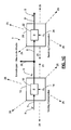
- FIG. 1A illustrates a traditional cryptographic model 2 involving secure communications between a sending correspondent 10 and a receiving correspondent 20 over a communication channel 8.
- a message M 5 is taken as input 7 by the sending correspondent 10.
- the sending correspondent 10 applies an encrypting cryptographic operation 12 that includes an encryption key K E 14 as a private (secret) value.
- the encrypted message M E 6 may be communicated securely over an open communication channel 8 to the receiving correspondent 20.
- the receiving correspondent 20 may apply a decrypting cryptographic operation 22 that includes a decryption key K D 24 to recover the M 5 as output 9.
- Figure 1B illustrates the traditional cryptographic model 2 of Figure 1A , further including an eavesdropper 30 that may intercept the encrypted message M E 6 as it is transmitted over the communication channel 8.
- the potential success of an interception attack of this type may typically be predicted from the theoretical strength of the encrypting cryptographic operation 12 being employed.
- Figure 1C illustrates the model of Figure 1B and further including side-channel information 25 that is physically emanating from the sending computing device 14 and the receiving computing device 24.
- the side-channel information 25 will be correlated to sub-steps of the cryptographic operation.
- An attacker may collect the side-channel information 25 and, in combination with an understanding of the underlying cryptographic process, may apply statistical methods to the side-channel information 25 to break the cryptographic process.
- a common side-channel attack includes measuring the electric field generated by the computing device when values are stored in registers of the computing device. These measurements provide timing information, as well as providing some information regarding the size of a value and whether a value has changed between operations or for repeated calculations using the same input value.
- a cryptographic operation 26 may generate side-channel information.
- the side-channel information may be masked by a noise source, such as a Linear Feedback Shift Register (LFSR), that generates a random number each clock cycle.
- LFSR Linear Feedback Shift Register
- a noise register 28 is connected to a pseudo-random number generator 29 that supplies a random number each clock cycle.
- the generated random number emanates its own signal, the power of which is determined by the size of the register 28 (ie the number of bits in the number) and the operation of the pseudo-random number generator 29, such as the switching of components like XOR gates.
- the noise additive circuit 30 comprises one or more dummy operations 36 that operate in parallel to the cryptographic operation 34.
- an input value 31 may be stored in a register 32 and delivered to both the cryptographic operations 34 and the dummy operations 36. Only the output 35 from the cryptographic operations 34 is passed on for further processing by the computing device.
- the dummy operations 36 are preferably unrelated to the input data 31 or any cryptographic keys used in the cryptographic operations 34, but may be physically close to the cryptographic operations 34.
- the one or more dummy operations 36 preferably generate random background noise, rather than a repetitive signal that may be filtered out by an attacker.
- the power of the noise signal is dependent upon a number of dummy operations 36 and a size of any numbers stored in registers that form part of the dummy operations 36.
- a further approach is to employ a ring oscillator whose output randomly oscillates between two voltage levels (e.g. TRUE and FALSE).
- a potential limitation of the ring oscillator is that the power dissipation is a related to the frequency of the oscillation. Effectively, where a ring oscillator is oscillating at the clock speed of the board, the power dissipation is a fixed value. The level of power can be increased by either increasing the number of ring oscillators, or increasing the oscillation frequency of the ring oscillator.
- patent EP 1 571 529 discloses: A hardware countermeasure against side-channel attacks for a cryptographic hardware module of a computing device, the hardware countermeasure comprising a distributed buffer network co-located with the cryptographic module, wherein the distributed buffer network is operable to accept as input a security level and to emit a noise output proportional in power to the power level associated with that security level, by activating a number of buffers of the distributed buffer network corresponding to the power level (see fig. 1 and par. 0047-0048).
- AWGN Additive White Gaussian Noise
- All processes being executed on a computing device generate a signal.
- An attacker can isolate the signal emitted by cryptographic operations by locating a capture antenna physically closest to the cryptographic operations, and/or by applying signal processing techniques to the captured signal to enhance the cryptographic signal and suppress the background or control operation signal.
- These signal processing techniques can typically be applied to suppress AWGN noise signals, for instance by collecting a number of sample measurements from the computing device. Over time, and a sufficient number of sample measurements, the AWGN signal will tend to average to a constant (positive value, negative value or zero) regardless of a number of sample measurements collected or a time of collection. For instance, for AWGN noise, an average m 1 for 1000 collected samples may have a value of c and an average m 2 for 2000 collected samples also has the value c.
- AWGN sources are an imperfect solution for countering side channel analysis attacks, and require that the power dissipated be high enough to cover the underlying cryptographic operations.
- the above methods generally provide either a limited power dissipation level, and/or are not constructed of standard CMOS architecture.
- a hardware countermeasure is provided that improves the resistance of a computing device, such as a hardware cryptographic module, to side channel attack.
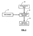
- an entropy source 38 such as a pseudo-random number generator, generates random values.
- the random values and data samples 37 to be processed by the cryptographic hardware module are input to a noise-sample generator 40.
- the noise-sample generator 40 accepts as input the random values, shown as being generated from an entropy source 38, and the data samples 37, and generates as output, a noise-sample for each input data sample.
- the noise-sample being associated with a power level of a noise output to be emitted by the hardware countermeasure.
- the series of noise-samples may comprise non-Gaussian noise-samples.
- an average computed from collected samples will change over time, based on a number of measurements and a time of collecting the samples.
- a magnitude of each of c 1 and c 2 are larger than a magnitude of c.
- the noise-samples from the noise-sample generator 40 are used to drive a distributed buffer network 52 that generates a noise output proportional in emitted power to a power level associated with each input noise-sample.
- the entropy source 38 and noise-sample generator 40 may be physically located elsewhere on the computing device, but the distributed buffer network 52 is preferably co-located with the hardware cryptographic module and most preferably co-located with any sensitive operations to be performed by the hardware cryptographic module, such as a hardware masking or de-masking operation.
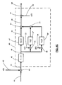
- a sample input 41 such as a data sample being input into a cryptographic module, is preferably masked 43 with a sample from a random data sequence ⁇ (t) 42.
- the random data sequence ⁇ (t) 42 may be generated from an entropy source 38, as illustrated in Figure 3 .
- the sample input 41 may comprise, for instance, a parallel output from an input register to the cryptographic module.
- the masking operation 43 may be considered to occur before (as illustrated) or as part of the noise-sample generator 40.
- the masked sample input 44 may then be operated upon by the noise-sample generator 40 to generate a noise-sample output 50.
- the noise-sample output 50 being associated with a noise output power level to be emitted by the hardware countermeasure.
- the noise-sample generator may comprise, for instance a digital filter having one or more coefficients.
- the masked sample input 44 may first be operated on by a difference operation 45, generating a difference 46 between a current sample and previous sample.
- the difference operation 45 is optional in an embodiment of the noise-sample generator 40.
- the difference 46 may then be input into a filter operation h(t) 47 to generate a filtered sample 48.
- the filtered sample 48 may optionally be further operated on by a masking operation 51, shown as an additive masking operation in Figure 4 , by combination with a sample from a random data masking sequence ⁇ (t) 52.
- the embodiment of Figure 4B illustrates an optional arrangement, where the difference 46 may be further operated in parallel by a plurality of filter operations h(t) 47, h ⁇ (t) 57 and h ⁇ (t) 58 .
- the difference 46 may be split between the plurality of filter operations h(t) 47, h ⁇ (t) 57 and h ⁇ (t) 58, filtered and combined, for instance through an additive operation 51b, to generate a combined filtered sample 49 that may be masked in masking operation 51 with the random data masking sequence ⁇ (t) 52.
- the difference 46 may be masked in a masking operation before input to one or more of the filter operations h(t) 47, h ⁇ (t) 57 and h ⁇ (t) 58.
- the difference 46 may be masked with filter masking operations 55, 56 before some of the plurality of filter operations h ⁇ (t) 57 and h ⁇ (t) 58 to avoid operating on the same input in each of the plurality of filter operations h(t) 47, h ⁇ (t) 57 and h ⁇ (t) 58.
- each of the filter masking operations 55, 56 comprise an XOR operation, combining the difference 46 with a sample from a random data sequence ⁇ (t) 53, ⁇ (t) 54.
- the filter operations h(t) 47, h ⁇ (t) 57 and h ⁇ (t) 58 may comprise, for instance, a Finite Impulse Response (FIR) filter.
- the filter coefficients may differ between each of the filter operations h(t) 47, h ⁇ (t) 57 and h ⁇ (t) 58 and in an aspect are selected randomly or pseudo-randomly.
- the filter coefficients may further be re-set after one or more cryptographic operations or "execution traces" performed by the cryptographic module.
- the filter coefficients may be determined by at least one look-up table containing pseudo random data that has been selected for optimum filter operations according to known signal processing techniques.
- the filter coefficients may be updated by selecting either a next set of filter coefficients, or a random set of filter coefficients from the at least one look-up table. The selection may occur either after a pre-selected number of cryptographic operations, or according to some other trigger criteria, such as after a random number of operations or a period of time.
- the filters may employ a coefficient word length of about 6 bits and the filters may comprise 7 th order filters having 8 coefficients, though other combinations of word lengths and filter order are contemplated and may be selected depending upon the application and level of complexity required.
- the outputs from the plurality of filter operations h(t) 47, h ⁇ (t) 57 and h ⁇ (t) 58 may be combined, for instance through addition operations 51b to generate the combined filtered sample 49.
- the combined filtered sample 49 may be combined in a masking operation 51 with the sample from the random data masking sequence ⁇ (t) 52 to generate the noise-sample output 50.
- FIG. 4C illustrates an alternative optional arrangement, comprising three filter operations h(t,w) 47', h t (t) 57' the first order partial derivative of h(t,w) 47' with respect to t, and h w (t) 58' the first order partial derivative of h(t,w) 47' with respect to w.
- the three filter operations h(t,w) 47', h t (t) 57', and h w (t) 58' generate a non-Gaussian noise-sample output 50'.
- the noise-sample generator 40 accepts as input a sample input 41
- the non-Gaussian noise-sample output 50' preferably is not correlated to the sample input 41.
- the noise-sample output 50 may comprise, for instance, a binary number that is received as input by a noise generation component such as a distributed buffer network 52.
- the distributed buffer network 52 may take as input the noise-sample output 50, or non-Gaussian noise-sample output 50', from the noise-sample generator 40 and dissipate a noise output having a power level that corresponds to a value of the input noise-sample 50 50'.
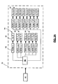
- the noise-sample generator 40 may send noise-sample outputs to the distributed buffer network 52, which may comprise a plurality of buffers 82.
- Each of the plurality of buffers 82 may be connected with a corresponding capacitive load 83.
- the corresponding capacitive load 83 determined by a size of that buffer 82 and a required response time for the buffer 82 as dictated by a board speed of the hardware, as would be understood by a person skilled in the art.
- a combination of a buffer 82 connected with the corresponding capacitive load 83 may dissipate a noise output having a magnitude determined by a size of the buffer 82 and the corresponding capacitive load 83.
- control logic 80 is operable to activate some of the n buffer blocks 84, 85, 86, 87 in response to noise-samples received from the noise-sample generator 40.
- each noise-sample corresponds to a noise output power level to be output by the buffer network 52.
- each noise-sample corresponds to a number of buffers 82, or combination of buffer blocks 84, 85, 86, 87 to be activated by the distributed buffer network 52.
- control logic 80 may activate different combinations of the buffer blocks 84, 85, 86 & 87, where the i th bit of the noise-sample value controls a one of the buffer blocks 84, 85, 86 & 87 generating a noise power proportional to 2 i .
- each buffer 82 is assumed to be of a same buffer size. Accordingly, a noise power level dissipated by each buffer block 84, 85, 86 & 87 may be determined by multiplying a reference buffer power value P ref times a number of buffers 82 in that buffer block 84, 85, 86, 87.
- one or more of the buffers 82 may comprise buffers 82 of a different size, such that a buffer noise power level may vary according to a size of the one or more buffers 82.
- a power of the buffer blocks 84, 85, 86, 87controlled by each bit of the noise-sample value is illustrated as an embodiment, and other combinations of bits and buffer blocks 84, 85, 86, 87 for emitting noise are contemplated.
- Table 1 provides different noise power levels, as well as differing locations of noise generation from the distributed buffer network 52.
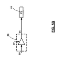
- a buffer may comprise a tri-state buffer 88.
- the tri-state buffer 88 accepts as input the noise-sample, or a corresponding bit of the noise-sample for that tri-state buffer 88, through a control input 90.
- the tri-state buffer 88 further comprises an enabling input 89 that may, for instance, take as input a timing signal to trigger activation of the tri-state buffer 88.
- the timing signal may comprise, for instance, a clock signal clocked to the operations of the hardware module 60.
- the clock signal enable the tri-state buffer 88 to activate at the same clock timing as the hardware operations to be masked by the distributed buffer network 52.
- the clock signal may specifically comprise a local clock signal connected to hardware components adjacent to a corresponding buffer network 52.
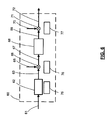
- a hardware module 60 such as a cryptographic hardware module, or a portion of a general hardware module that has been dedicated to secure operations such as cryptographic operations is illustrated.
- An input 61 to the hardware module 60 may comprise input data to be processed by the hardware module 60.
- the input 61 may optionally be transferred to an input register 62 for temporary storage before the stored input 63 is operated on by an input cryptographic operation 66, such as the masking operation illustrated in Figure 6 .
- An input mask 65 is shown as being applied during the input cryptographic operation 66, which produces a masked input 67 that may be operated on by masked cryptographic operations 68.
- a masked result 69 of the masked cryptographic operations 68 may be operated on by an output cryptographic operation 71, such as the de-masking operation illustrated in Figure 6 .
- An output mask 70 is shown as being applied during the output cryptographic operation 71, which produces the unmasked result 72 for transfer out of the hardware module 60.
- At least one of the plurality of buffers 75, and the corresponding capacitive load may be located adjacent to a register within the cryptographic module, such as the input register 62 of the hardware module 60.
- at least one of the plurality of buffers, and the corresponding capacitive load may be co-located with internal registers, not shown in Figure 6 , of the cryptographic module that receive input data samples that are to be operated on by the cryptographic module.
- sensitive data is input into the cryptographic hardware module and, typically, stored in an input register 62 such as a sensitive data input register.
- the sensitive data input register 62 supplies the input sample for an initial cryptographic operation 66, such as a masking operation. Since the sensitive data input may typically have been output from another component of the computing device to the sensitive data input register 62 of the cryptographic module 60, it is possible for an attacker to localize and match the sensitive data input located in the other component with the sensitive data input located in the sensitive data input register 62.
- At least one of the plurality of buffers 75, and the corresponding capacitive load may be co-located with the sensitive data input register 62 such that the countermeasure is operable to protect values stored in the sensitive data input register 62 from side channel analysis.
- a plurality of buffers 75 from the distributed buffer network 75 may be co-located with the sensitive data input register 62.
- data samples input to the hardware module 60 from the computing device including data samples such as encrypted data, date/time, random data, etc., may be protected.
- other registers within the hardware module 60 may be required to receive the input data for operation on by the hardware module 60.
- At least one of the plurality of buffers 76, and the corresponding capacitive load may be located adjacent to a hardware block of the hardware module 60 that performs a cryptographic operation 66, such as the masking operation illustrated.
- the sensitive data input register 62 may supply an input value for operation in a masked cryptographic operation of the hardware module 60.
- An initial cryptographic operation 66 may consist of masking the input value in order to execute the masked cryptographic operation.
- at least one of the plurality of buffers 76, and the corresponding capacitive load(s) may be located adjacent to the hardware components that perform the cryptographic operation 66.
- At least one of the plurality of buffers 77, and the corresponding capacitive load may be located adjacent to a hardware block of the hardware module 60 that performs a subsequent cryptographic operation 71, such as the de-masking operation illustrated.
- the subsequent cryptographic operation 71 may consist of the removal of a random mask from an output data sample 69 operated on by the masked cryptographic operation 68.
- the hardware module 60 may remove the mask by applying a de-masking mask 70 in the subsequent cryptographic operation 71 to yield an unmasked result 72 of the masked cryptographic operation 68 (such as encrypted or decrypted data) for output from the hardware module 60 to the computing device.
- Co-locating the at least one of the plurality of buffers 77 with the de-masking operation protects against providing information about the mask that was used in the masked cryptographic operation 68.
- the at least one of the plurality of buffers and the corresponding capacitive load may be located adjacent to a mask modification hardware block of a hardware module 60 that performs a mask modification operation to update a mask of a masking operation. Co-locating the at least one of the plurality of buffers with the mask modification operation protects against providing information about the mask that was used in the masked cryptographic operation.
- the mask modification hardware block may in an aspect be located, for instance, proximate to the cryptographic operation 66, shown as a masking operation, or the subsequent cryptographic operation 71, shown as a de-masking operation. In an alternate aspect, the mask modification hardware block may be located at another location within the hardware module 60.
- the distributed buffer network may be built with a standard CMOS structure. Accordingly, the buffers and corresponding capacitive load may be formed using the same silicon process as the rest of the cryptographic hardware module and co-located with either data registers, or cryptographic logic hardware blocks of the cryptographic hardware module. For instance, a register block within the cryptographic hardware module may start with register bits that contain a data sample, and end with register bits that comprise one or more of the buffers of a distributed buffer network. The one or more of the buffers of the distributed buffer network may each be located adjacent to a corresponding capacitive load. Constructing the distributed buffer network with a standard CMOS structure may reduce cost, reduce the size of a cryptographic hardware module containing the hardware countermeasure and improve its resistance to side channel analysis.
- the noise-sample generated by the noise-sample generator 40 may comprise a binary number.
- each bit of the binary number may control one or more buffers of the distributed buffer network. Accordingly, a power level of noise generated by the distributed buffer network may not increase linearly with a number of bits contained in each noise-sample.
- the bits may cause activation of the one or more buffers that correspond to that bit of the noise-sample.
Landscapes
- Engineering & Computer Science (AREA)
- Physics & Mathematics (AREA)
- Computer Hardware Design (AREA)
- Theoretical Computer Science (AREA)
- Mathematical Physics (AREA)
- Computer Security & Cryptography (AREA)
- Software Systems (AREA)
- General Engineering & Computer Science (AREA)
- General Physics & Mathematics (AREA)
- Mobile Radio Communication Systems (AREA)
- Storage Device Security (AREA)
Claims (16)
- Eine Hardware-Gegenmaßnahme gegen Seitenkanalangriffe für ein kryptographisches Hardware-Modul einer Computervorrichtung, wobei die Hardware-Gegenmaßnahme aufweist:einen Rauschen-Abtast-Generator, wobei der Rauschen-Abtast-Generator betriebsfähig ist zum Annehmen von Datenabtastwerten, die von dem kryptographischen Hardware-Modul zu verarbeiten sind, als Eingabe und zum Erzeugen als Ausgabe eines Rauschen-Abtastwerts für jeden der Eingangsdatenabtastwerte, und wobei der Rauschen-Abtastwert mit einem Leistungspegel assoziiert ist; undein verteiltes Puffernetzwerk, das mit dem kryptographischen Modul co-loziert ist, wobei das verteilte Puffernetzwerk betriebsfähig ist zum Annehmen der Rauschen-Abtastwerte als Eingabe und zum Emittieren, für jeden der Rauschen-Abtastwerte, einer Rauschenausgabe proportional in der Leistung zu dem Leistungspegel, der mit diesem Rauschen-Abtastwert assoziiert ist, durch Aktivieren einer Anzahl von Puffern des verteilten Puffernetzwerks entsprechend dem Leistungspegel.
- Die Hardware-Gegenmaßnahme gemäß Anspruch 1, wobei jeder der Vielzahl von Puffern mit einer entsprechenden kapazitiven Last verbunden ist.
- Die Hardware-Gegenmaßnahme gemäß Anspruch 2, wobei sich zumindest einer der Vielzahl von Puffern und die entsprechende(n) kapazitive(n) Last(en) angrenzend an ein Eingangsregister des kryptographischen Hardware-Moduls befinden.
- Die Hardware-Gegenmaßnahme gemäß Anspruch 2, wobei sich zumindest einer der Vielzahl von Puffern und die entsprechende(n) kapazitive(n) Last(en) angrenzend an einen Hardwareblock des kryptografischen Moduls befinden, das eine Maskierungsoperation durchführt.
- Die Hardware-Gegenmaßnahme gemäß Anspruch 4, wobei die Maskierungsoperation entweder die Anwendung einer Zufallsmaske auf einen Eingangsdatenabtastwert für eine Operation durch eine kryptographische Operation oder die Entfernung einer Zufallsmaske von einem Ausgangsdatenabtastwert aufweist, verarbeitet durch die kryptographische Operation.
- Die Hardware-Gegenmaßnahme gemäß Anspruch 2, wobei sich zumindest einer der Vielzahl von Puffern und die entsprechende(n) kapazitive(n) Last(en) angrenzend an einen Hardwareblock des kryptografischen Moduls befinden, das eine Maskierungsmodifizierungsoperation durchführt, um eine Maske einer Maskierungsoperation zu aktualisieren.
- Die Hardware-Gegenmaßnahme gemäß Anspruch 1, wobei das verteilte Puffernetzwerk aus einer Standard-CMOS-Struktur aufgebaut ist und mit zumindest einem kryptographischen Logik-Hardwareblock des kryptographischen Hardware-Moduls co-loziert ist.
- Die Hardware-Gegenmaßnahme gemäß Anspruch 1, wobei der Rauschen-Abtastwert eine Binärzahl aufweist und jedes Bit der Binärzahl einem oder mehreren Puffer(n) des verteilten Puffernetzwerks entspricht, um den Leistungspegel zu setzen.
- Die Hardware-Gegenmaßnahme gemäß Anspruch 8, wobei das verteilte Puffernetzwerk betriebsfähig ist zum Emittieren der Rauschenausgabe durch Aktivieren des einen oder der mehreren Puffer(s), der/die jedem Bit der Binärzahl entspricht/entsprechen.
- Die Hardware-Gegenmaßnahme gemäß Anspruch 9, wobei der eine oder die mehreren Puffer eine zunehmende Anzahl von Puffern entsprechend einer Signifikanz jedes Bits aufweist/aufweisen.
- Die Hardware-Gegenmaßnahme gemäß Anspruch 1, wobei die Rauschen-Abtastwerte, die von dem Rauschen-Abtast-Ausgabe-Generator ausgegeben werden, nicht-Gaußsche Rauschen-Abtastwerte aufweisen.
- Die Hardware-Gegenmaßnahme gemäß Anspruch 1, wobei das verteilte Puffernetzwerk eine Vielzahl von Pufferblöcken aufweist, wobei jeder der Vielzahl von Pufferblöcken zumindest einen Puffer aufweist, und wobei das verteilte Puffernetzwerk betriebsfähig ist zum Emittieren der Rauschenausgabe durch Aktivieren einer Kombination der Vielzahl von Pufferblöcken entsprechend dem Leistungspegel.
- Die Hardware-Gegenmaßnahme gemäß Anspruch 12, wobei jeder der Vielzahl von Pufferblöcken eine andere Anzahl von Puffern aufweist.
- Die Hardware-Gegenmaßnahme gemäß Anspruch 12, wobei jeder der Vielzahl von Pufferblöcken einen anderen Rauschleistungspegel dissipiert.
- Die Hardware-Gegenmaßnahme gemäß Anspruch 12, wobei der Rauschen-Abtastwert eine Binärzahl aufweist und jedes Bit der Binärzahl einem der Vielzahl von Pufferblöcken entspricht.
- Eine mobile Kommunikationsvorrichtung, die die Hardware-Gegenmaßnahme gemäß Anspruch 1 aufweist.
Applications Claiming Priority (1)
| Application Number | Priority Date | Filing Date | Title |
|---|---|---|---|
| US13/283,472 US8627131B2 (en) | 2011-10-27 | 2011-10-27 | Hardware countermeasure against cryptographic attack |
Publications (2)
| Publication Number | Publication Date |
|---|---|
| EP2587402A1 EP2587402A1 (de) | 2013-05-01 |
| EP2587402B1 true EP2587402B1 (de) | 2015-10-14 |
Family
ID=45607593
Family Applications (1)
| Application Number | Title | Priority Date | Filing Date |
|---|---|---|---|
| EP12152533.1A Active EP2587402B1 (de) | 2011-10-27 | 2012-01-25 | Hardwaregegenmaßnahme gegen kryptographische Angriffe |
Country Status (3)
| Country | Link |
|---|---|
| US (1) | US8627131B2 (de) |
| EP (1) | EP2587402B1 (de) |
| CA (1) | CA2793492C (de) |
Families Citing this family (7)
| Publication number | Priority date | Publication date | Assignee | Title |
|---|---|---|---|---|
| DE102015211108A1 (de) * | 2015-06-17 | 2016-12-22 | Robert Bosch Gmbh | Vorrichtung und Verfahren zur Ausführung eines Rechenverfahrens |
| GB2544452B (en) * | 2015-08-26 | 2019-09-11 | Advanced Risc Mach Ltd | Data processing systems |
| DE102016119750B4 (de) * | 2015-10-26 | 2022-01-13 | Infineon Technologies Ag | Vorrichtungen und Verfahren zur Mehrkanalabtastung |
| WO2019116370A1 (en) * | 2017-12-13 | 2019-06-20 | B. G. Negev Technologies And Applications Ltd., At Ben-Gurion University | Echo detection of man-in-the-middle lan attacks |
| US11303462B2 (en) | 2018-11-19 | 2022-04-12 | Arizona Board Of Regents On Behalf Of Northern Arizona University | Unequally powered cryptography using physical unclonable functions |
| US11675899B2 (en) | 2020-12-15 | 2023-06-13 | International Business Machines Corporation | Hardware mitigation for Spectre and meltdown-like attacks |
| US12487280B2 (en) * | 2023-04-26 | 2025-12-02 | Intel Corporation | Apparatuses, methods and computer programs for executing an executable, and method for distributing software or firmwares |
Family Cites Families (6)
| Publication number | Priority date | Publication date | Assignee | Title |
|---|---|---|---|---|
| US6748410B1 (en) * | 1997-05-04 | 2004-06-08 | M-Systems Flash Disk Pioneers, Ltd. | Apparatus and method for modular multiplication and exponentiation based on montgomery multiplication |
| EP2280502B1 (de) | 1998-06-03 | 2018-05-02 | Cryptography Research, Inc. | Verwenden von unvorhersehbaren Informationen zu widerstehen die Entdeckung von Geheimnissen durch externe Überwachung |
| EP1293856A1 (de) | 2001-09-18 | 2003-03-19 | EM Microelectronic-Marin SA | Geschützte integrierte Schaltung mit vertraulichen Teilen und Verfahren zur Aktivierung dieser Schaltung |
| FR2863746B1 (fr) | 2003-12-10 | 2006-08-11 | Innova Card | Circuit integre protege par bouclier actif |
| JP4674440B2 (ja) | 2004-03-04 | 2011-04-20 | ソニー株式会社 | データ処理回路 |
| US20120124669A1 (en) * | 2010-11-12 | 2012-05-17 | International Business Machines Corporation | Hindering Side-Channel Attacks in Integrated Circuits |
-
2011
- 2011-10-27 US US13/283,472 patent/US8627131B2/en active Active
-
2012
- 2012-01-25 EP EP12152533.1A patent/EP2587402B1/de active Active
- 2012-10-29 CA CA2793492A patent/CA2793492C/en active Active
Also Published As
| Publication number | Publication date |
|---|---|
| CA2793492C (en) | 2016-04-19 |
| CA2793492A1 (en) | 2013-04-27 |
| US8627131B2 (en) | 2014-01-07 |
| US20130111204A1 (en) | 2013-05-02 |
| EP2587402A1 (de) | 2013-05-01 |
Similar Documents
| Publication | Publication Date | Title |
|---|---|---|
| CA2793492C (en) | Hardware countermeasure against cryptographic attack | |
| Krautter et al. | Active fences against voltage-based side channels in multi-tenant FPGAs | |
| Barenghi et al. | Fault injection attacks on cryptographic devices: Theory, practice, and countermeasures | |
| Dofe et al. | Hardware security assurance in emerging IoT applications | |
| CN105940439B (zh) | 使用排列应对对密码算法的旁通道攻击的对策 | |
| EP3143720B1 (de) | Differenzielle leistungsanalysegegenmassnahmen | |
| KR102794580B1 (ko) | 메시지 부호화 및 복호화를 위한 블록 암호화 방법 및 이 방법을 구현하기 위한 암호화 장치 | |
| US8804949B2 (en) | Method for protecting IC cards against power analysis attacks | |
| Bedoui et al. | An improvement of both security and reliability for AES implementations | |
| Kalenderi et al. | Breaking the GSM A5/1 cryptography algorithm with rainbow tables and high-end FPGAS | |
| Liu et al. | A true random-based differential power analysis countermeasure circuit for an AES engine | |
| Liu et al. | Scan-based attacks on linear feedback shift register based stream ciphers | |
| CN112906070A (zh) | 用于安全设备的块密码侧信道攻击减轻 | |
| Moraitis et al. | Securing CRYSTALS-kyber in FPGA using duplication and clock randomization | |
| Lagasse et al. | Combining clock and voltage noise countermeasures against power side-channel analysis | |
| Huang et al. | Trace buffer attack on the AES cipher | |
| Moraitis et al. | A side-channel resistant implementation of AES combining clock randomization with duplication | |
| Surya et al. | Local clock glitching fault injection with application to the ASCON cipher | |
| Ewert et al. | Lightweight authenticated integration and in-field secure operation of system-in-package | |
| Guo et al. | EOP: An encryption-obfuscation solution for protecting PCBs against tampering and reverse engineering | |
| Bidmeshki et al. | Hardware-based attacks to compromise the cryptographic security of an election system | |
| Moradi | Advances in side-channel security | |
| US20260023533A1 (en) | Ring-generator-based true random number generator for hardware root of trust | |
| US11436346B2 (en) | Device for protecting encrypted data and associated method | |
| Korkikian | Side-channel and fault analysis in the presence of countermeasures: tools, theory, and practice |
Legal Events
| Date | Code | Title | Description |
|---|---|---|---|
| PUAI | Public reference made under article 153(3) epc to a published international application that has entered the european phase |
Free format text: ORIGINAL CODE: 0009012 |
|
| 17P | Request for examination filed |
Effective date: 20120125 |
|
| AK | Designated contracting states |
Kind code of ref document: A1 Designated state(s): AL AT BE BG CH CY CZ DE DK EE ES FI FR GB GR HR HU IE IS IT LI LT LU LV MC MK MT NL NO PL PT RO RS SE SI SK SM TR |
|
| AX | Request for extension of the european patent |
Extension state: BA ME |
|
| GRAP | Despatch of communication of intention to grant a patent |
Free format text: ORIGINAL CODE: EPIDOSNIGR1 |
|
| INTG | Intention to grant announced |
Effective date: 20150402 |
|
| GRAS | Grant fee paid |
Free format text: ORIGINAL CODE: EPIDOSNIGR3 |
|
| GRAA | (expected) grant |
Free format text: ORIGINAL CODE: 0009210 |
|
| RAP1 | Party data changed (applicant data changed or rights of an application transferred) |
Owner name: CERTICOM CORP. |
|
| AK | Designated contracting states |
Kind code of ref document: B1 Designated state(s): AL AT BE BG CH CY CZ DE DK EE ES FI FR GB GR HR HU IE IS IT LI LT LU LV MC MK MT NL NO PL PT RO RS SE SI SK SM TR |
|
| REG | Reference to a national code |
Ref country code: GB Ref legal event code: FG4D |
|
| REG | Reference to a national code |
Ref country code: AT Ref legal event code: REF Ref document number: 755616 Country of ref document: AT Kind code of ref document: T Effective date: 20151015 Ref country code: CH Ref legal event code: EP |
|
| REG | Reference to a national code |
Ref country code: IE Ref legal event code: FG4D |
|
| REG | Reference to a national code |
Ref country code: DE Ref legal event code: R096 Ref document number: 602012011458 Country of ref document: DE |
|
| REG | Reference to a national code |
Ref country code: FR Ref legal event code: PLFP Year of fee payment: 5 |
|
| REG | Reference to a national code |
Ref country code: NL Ref legal event code: MP Effective date: 20151014 |
|
| REG | Reference to a national code |
Ref country code: LT Ref legal event code: MG4D |
|
| REG | Reference to a national code |
Ref country code: AT Ref legal event code: MK05 Ref document number: 755616 Country of ref document: AT Kind code of ref document: T Effective date: 20151014 |
|
| PG25 | Lapsed in a contracting state [announced via postgrant information from national office to epo] |
Ref country code: ES Free format text: LAPSE BECAUSE OF FAILURE TO SUBMIT A TRANSLATION OF THE DESCRIPTION OR TO PAY THE FEE WITHIN THE PRESCRIBED TIME-LIMIT Effective date: 20151014 Ref country code: HR Free format text: LAPSE BECAUSE OF FAILURE TO SUBMIT A TRANSLATION OF THE DESCRIPTION OR TO PAY THE FEE WITHIN THE PRESCRIBED TIME-LIMIT Effective date: 20151014 Ref country code: IT Free format text: LAPSE BECAUSE OF FAILURE TO SUBMIT A TRANSLATION OF THE DESCRIPTION OR TO PAY THE FEE WITHIN THE PRESCRIBED TIME-LIMIT Effective date: 20151014 Ref country code: IS Free format text: LAPSE BECAUSE OF FAILURE TO SUBMIT A TRANSLATION OF THE DESCRIPTION OR TO PAY THE FEE WITHIN THE PRESCRIBED TIME-LIMIT Effective date: 20160214 Ref country code: NL Free format text: LAPSE BECAUSE OF FAILURE TO SUBMIT A TRANSLATION OF THE DESCRIPTION OR TO PAY THE FEE WITHIN THE PRESCRIBED TIME-LIMIT Effective date: 20151014 Ref country code: NO Free format text: LAPSE BECAUSE OF FAILURE TO SUBMIT A TRANSLATION OF THE DESCRIPTION OR TO PAY THE FEE WITHIN THE PRESCRIBED TIME-LIMIT Effective date: 20160114 Ref country code: LT Free format text: LAPSE BECAUSE OF FAILURE TO SUBMIT A TRANSLATION OF THE DESCRIPTION OR TO PAY THE FEE WITHIN THE PRESCRIBED TIME-LIMIT Effective date: 20151014 |
|
| PG25 | Lapsed in a contracting state [announced via postgrant information from national office to epo] |
Ref country code: AT Free format text: LAPSE BECAUSE OF FAILURE TO SUBMIT A TRANSLATION OF THE DESCRIPTION OR TO PAY THE FEE WITHIN THE PRESCRIBED TIME-LIMIT Effective date: 20151014 Ref country code: LV Free format text: LAPSE BECAUSE OF FAILURE TO SUBMIT A TRANSLATION OF THE DESCRIPTION OR TO PAY THE FEE WITHIN THE PRESCRIBED TIME-LIMIT Effective date: 20151014 Ref country code: FI Free format text: LAPSE BECAUSE OF FAILURE TO SUBMIT A TRANSLATION OF THE DESCRIPTION OR TO PAY THE FEE WITHIN THE PRESCRIBED TIME-LIMIT Effective date: 20151014 Ref country code: RS Free format text: LAPSE BECAUSE OF FAILURE TO SUBMIT A TRANSLATION OF THE DESCRIPTION OR TO PAY THE FEE WITHIN THE PRESCRIBED TIME-LIMIT Effective date: 20151014 Ref country code: GR Free format text: LAPSE BECAUSE OF FAILURE TO SUBMIT A TRANSLATION OF THE DESCRIPTION OR TO PAY THE FEE WITHIN THE PRESCRIBED TIME-LIMIT Effective date: 20160115 Ref country code: BE Free format text: LAPSE BECAUSE OF NON-PAYMENT OF DUE FEES Effective date: 20160131 Ref country code: SE Free format text: LAPSE BECAUSE OF FAILURE TO SUBMIT A TRANSLATION OF THE DESCRIPTION OR TO PAY THE FEE WITHIN THE PRESCRIBED TIME-LIMIT Effective date: 20151014 Ref country code: PL Free format text: LAPSE BECAUSE OF FAILURE TO SUBMIT A TRANSLATION OF THE DESCRIPTION OR TO PAY THE FEE WITHIN THE PRESCRIBED TIME-LIMIT Effective date: 20151014 Ref country code: PT Free format text: LAPSE BECAUSE OF FAILURE TO SUBMIT A TRANSLATION OF THE DESCRIPTION OR TO PAY THE FEE WITHIN THE PRESCRIBED TIME-LIMIT Effective date: 20160215 |
|
| REG | Reference to a national code |
Ref country code: DE Ref legal event code: R097 Ref document number: 602012011458 Country of ref document: DE |
|
| PG25 | Lapsed in a contracting state [announced via postgrant information from national office to epo] |
Ref country code: CZ Free format text: LAPSE BECAUSE OF FAILURE TO SUBMIT A TRANSLATION OF THE DESCRIPTION OR TO PAY THE FEE WITHIN THE PRESCRIBED TIME-LIMIT Effective date: 20151014 |
|
| PLBE | No opposition filed within time limit |
Free format text: ORIGINAL CODE: 0009261 |
|
| STAA | Information on the status of an ep patent application or granted ep patent |
Free format text: STATUS: NO OPPOSITION FILED WITHIN TIME LIMIT |
|
| PG25 | Lapsed in a contracting state [announced via postgrant information from national office to epo] |
Ref country code: SM Free format text: LAPSE BECAUSE OF FAILURE TO SUBMIT A TRANSLATION OF THE DESCRIPTION OR TO PAY THE FEE WITHIN THE PRESCRIBED TIME-LIMIT Effective date: 20151014 Ref country code: DK Free format text: LAPSE BECAUSE OF FAILURE TO SUBMIT A TRANSLATION OF THE DESCRIPTION OR TO PAY THE FEE WITHIN THE PRESCRIBED TIME-LIMIT Effective date: 20151014 Ref country code: RO Free format text: LAPSE BECAUSE OF FAILURE TO SUBMIT A TRANSLATION OF THE DESCRIPTION OR TO PAY THE FEE WITHIN THE PRESCRIBED TIME-LIMIT Effective date: 20151014 Ref country code: EE Free format text: LAPSE BECAUSE OF FAILURE TO SUBMIT A TRANSLATION OF THE DESCRIPTION OR TO PAY THE FEE WITHIN THE PRESCRIBED TIME-LIMIT Effective date: 20151014 Ref country code: SK Free format text: LAPSE BECAUSE OF FAILURE TO SUBMIT A TRANSLATION OF THE DESCRIPTION OR TO PAY THE FEE WITHIN THE PRESCRIBED TIME-LIMIT Effective date: 20151014 Ref country code: LU Free format text: LAPSE BECAUSE OF FAILURE TO SUBMIT A TRANSLATION OF THE DESCRIPTION OR TO PAY THE FEE WITHIN THE PRESCRIBED TIME-LIMIT Effective date: 20160125 |
|
| REG | Reference to a national code |
Ref country code: CH Ref legal event code: PL |
|
| 26N | No opposition filed |
Effective date: 20160715 |
|
| PG25 | Lapsed in a contracting state [announced via postgrant information from national office to epo] |
Ref country code: MC Free format text: LAPSE BECAUSE OF FAILURE TO SUBMIT A TRANSLATION OF THE DESCRIPTION OR TO PAY THE FEE WITHIN THE PRESCRIBED TIME-LIMIT Effective date: 20151014 |
|
| PG25 | Lapsed in a contracting state [announced via postgrant information from national office to epo] |
Ref country code: LI Free format text: LAPSE BECAUSE OF NON-PAYMENT OF DUE FEES Effective date: 20160131 Ref country code: CH Free format text: LAPSE BECAUSE OF NON-PAYMENT OF DUE FEES Effective date: 20160131 |
|
| REG | Reference to a national code |
Ref country code: IE Ref legal event code: MM4A |
|
| PG25 | Lapsed in a contracting state [announced via postgrant information from national office to epo] |
Ref country code: SI Free format text: LAPSE BECAUSE OF FAILURE TO SUBMIT A TRANSLATION OF THE DESCRIPTION OR TO PAY THE FEE WITHIN THE PRESCRIBED TIME-LIMIT Effective date: 20151014 |
|
| PG25 | Lapsed in a contracting state [announced via postgrant information from national office to epo] |
Ref country code: BE Free format text: LAPSE BECAUSE OF FAILURE TO SUBMIT A TRANSLATION OF THE DESCRIPTION OR TO PAY THE FEE WITHIN THE PRESCRIBED TIME-LIMIT Effective date: 20151014 |
|
| REG | Reference to a national code |
Ref country code: FR Ref legal event code: PLFP Year of fee payment: 6 |
|
| PG25 | Lapsed in a contracting state [announced via postgrant information from national office to epo] |
Ref country code: IE Free format text: LAPSE BECAUSE OF NON-PAYMENT OF DUE FEES Effective date: 20160125 |
|
| PG25 | Lapsed in a contracting state [announced via postgrant information from national office to epo] |
Ref country code: MT Free format text: LAPSE BECAUSE OF FAILURE TO SUBMIT A TRANSLATION OF THE DESCRIPTION OR TO PAY THE FEE WITHIN THE PRESCRIBED TIME-LIMIT Effective date: 20151014 |
|
| REG | Reference to a national code |
Ref country code: FR Ref legal event code: PLFP Year of fee payment: 7 |
|
| PG25 | Lapsed in a contracting state [announced via postgrant information from national office to epo] |
Ref country code: CY Free format text: LAPSE BECAUSE OF FAILURE TO SUBMIT A TRANSLATION OF THE DESCRIPTION OR TO PAY THE FEE WITHIN THE PRESCRIBED TIME-LIMIT Effective date: 20151014 Ref country code: HU Free format text: LAPSE BECAUSE OF FAILURE TO SUBMIT A TRANSLATION OF THE DESCRIPTION OR TO PAY THE FEE WITHIN THE PRESCRIBED TIME-LIMIT; INVALID AB INITIO Effective date: 20120125 |
|
| PG25 | Lapsed in a contracting state [announced via postgrant information from national office to epo] |
Ref country code: MT Free format text: LAPSE BECAUSE OF FAILURE TO SUBMIT A TRANSLATION OF THE DESCRIPTION OR TO PAY THE FEE WITHIN THE PRESCRIBED TIME-LIMIT Effective date: 20160131 Ref country code: MK Free format text: LAPSE BECAUSE OF FAILURE TO SUBMIT A TRANSLATION OF THE DESCRIPTION OR TO PAY THE FEE WITHIN THE PRESCRIBED TIME-LIMIT Effective date: 20151014 Ref country code: TR Free format text: LAPSE BECAUSE OF FAILURE TO SUBMIT A TRANSLATION OF THE DESCRIPTION OR TO PAY THE FEE WITHIN THE PRESCRIBED TIME-LIMIT Effective date: 20151014 |
|
| PG25 | Lapsed in a contracting state [announced via postgrant information from national office to epo] |
Ref country code: BG Free format text: LAPSE BECAUSE OF FAILURE TO SUBMIT A TRANSLATION OF THE DESCRIPTION OR TO PAY THE FEE WITHIN THE PRESCRIBED TIME-LIMIT Effective date: 20151014 |
|
| PG25 | Lapsed in a contracting state [announced via postgrant information from national office to epo] |
Ref country code: AL Free format text: LAPSE BECAUSE OF FAILURE TO SUBMIT A TRANSLATION OF THE DESCRIPTION OR TO PAY THE FEE WITHIN THE PRESCRIBED TIME-LIMIT Effective date: 20151014 |
|
| REG | Reference to a national code |
Ref country code: DE Ref legal event code: R082 Ref document number: 602012011458 Country of ref document: DE Representative=s name: MERH-IP MATIAS ERNY REICHL HOFFMANN PATENTANWA, DE Ref country code: DE Ref legal event code: R081 Ref document number: 602012011458 Country of ref document: DE Owner name: BLACKBERRY LIMITED, WATERLOO, CA Free format text: FORMER OWNER: CERTICOM CORP., MISSISSAUGA, ONTARIO, CA |
|
| REG | Reference to a national code |
Ref country code: GB Ref legal event code: 732E Free format text: REGISTERED BETWEEN 20200206 AND 20200212 |
|
| REG | Reference to a national code |
Ref country code: DE Ref legal event code: R082 Ref document number: 602012011458 Country of ref document: DE Ref country code: DE Ref legal event code: R081 Ref document number: 602012011458 Country of ref document: DE Owner name: MALIKIE INNOVATIONS LTD., IE Free format text: FORMER OWNER: BLACKBERRY LIMITED, WATERLOO, ONTARIO, CA |
|
| PGFP | Annual fee paid to national office [announced via postgrant information from national office to epo] |
Ref country code: GB Payment date: 20260126 Year of fee payment: 15 |
|
| PGFP | Annual fee paid to national office [announced via postgrant information from national office to epo] |
Ref country code: DE Payment date: 20260127 Year of fee payment: 15 |
|
| PGFP | Annual fee paid to national office [announced via postgrant information from national office to epo] |
Ref country code: FR Payment date: 20260126 Year of fee payment: 15 |