EP2587337A2 - Electronic systems and power management methods thereof - Google Patents
Electronic systems and power management methods thereof Download PDFInfo
- Publication number
- EP2587337A2 EP2587337A2 EP20120179369 EP12179369A EP2587337A2 EP 2587337 A2 EP2587337 A2 EP 2587337A2 EP 20120179369 EP20120179369 EP 20120179369 EP 12179369 A EP12179369 A EP 12179369A EP 2587337 A2 EP2587337 A2 EP 2587337A2
- Authority
- EP
- European Patent Office
- Prior art keywords
- power
- electronic device
- mode
- electronic
- electronic devices
- Prior art date
- Legal status (The legal status is an assumption and is not a legal conclusion. Google has not performed a legal analysis and makes no representation as to the accuracy of the status listed.)
- Granted
Links
Images



Classifications
-
- G—PHYSICS
- G06—COMPUTING OR CALCULATING; COUNTING
- G06F—ELECTRIC DIGITAL DATA PROCESSING
- G06F1/00—Details not covered by groups G06F3/00 - G06F13/00 and G06F21/00
- G06F1/26—Power supply means, e.g. regulation thereof
- G06F1/266—Arrangements to supply power to external peripherals either directly from the computer or under computer control, e.g. supply of power through the communication port, computer controlled power-strips
Definitions
- the present invention relates to electronic systems, and in particular relates to electronic systems having high speed transmission interfaces.
- the invention provides an embodiment of an electronic system, comprising a plurality of electronic devices, a plurality of power supplies and a control module.
- the electronic devices each have a male connector and a female connector, wherein the male connectors are mated with the female connectors, such that the electronic devices are overlapped in a direction and electrically connected to each other.
- the power supplies are each connected to one of the electronic devices, respectively, for providing power to the electronic devices, wherein the number of the electronic devices is larger than the number of the power supplies.
- the control module has a first mode and a second mode to control the male connectors and the female connectors, wherein, in the first mode, a first electronic device of the electronic devices, which is not connected to either one of the power supplies, receives power through a first female connector of the first electronic device, and the first electronic device outputs power to another electronic device connected to a first male connector of the first electronic device through the first male connector.
- the invention also provides a power management method suitable for an electronic system having power supplies and electronic devices each of the electronic devices having a male connector and a female connector.
- the method comprises the steps of: determining whether one of the power supplies is connected to a first electronic device of the electronic devices which are electrically connected to each other and are overlapped in a direction, and receiving power from another electronic device of the electronic system through a first male connector or a first male connector of the first electronic device when the first electronic device is not connected to one of the power supplies, and providing the power to the first female connector or the first male connector.
- FIG.1 illustrates a schematic view of an electronic system of the disclosure
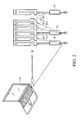
- FIG. 2 illustrates an embodiment of the first mode of the disclosure
- FIG. 3 illustrates an embodiment of the second mode of the disclosure
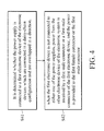
- FIG. 4 illustrates a first flowchart of the power management method of the disclosure
- FIG. 5 illustrates a second flowchart of the power management method of the disclosure.
- FIG.1 illustrates a schematic view of the electronic system of the disclosure.
- an electronic system 100 has electronic devices M1 ⁇ M6, a control module CM and power supplies P1 ⁇ P3.
- the two numbers of the electronic devices and the power supplies are provided for illustration, but are not limited thereto.
- the control module CM can be disposed in one of the electronic devices M1 ⁇ M6 or in a host 120 coupled to the electronic system 100 through a transmission cable, but is not limited thereto.
- the electronic devices M1 ⁇ M6 are overlapped in a direction.
- each of the electronic devices M1 ⁇ M6 has a high speed transmission interface, e.g., a thunderbolt interface, such that the electronic devices M1 ⁇ M6 use a transport protocol compatible with a thunderbolt interface to communicate with a host 120.
- the electronic devices M1 ⁇ M6 are coupled in a daisy-chain configuration.
- the data line DL is configured to deliver data when the electronic devices M1-M6 are electrically connected to each other.
- the male connector or the female connector of each of the electronic devices is connected to the female connector or the male connector of the other electronic device to form the power line PL, and the electronic devices M1-M6 provide power to each other through the power line PL.
- the control module CM has a first mode and a second mode to control switching units of the male connectors and the female connectors of the electronic devices M1-M6, such that each of the electronic devices can receive power through the male connector or the female connector, or each of the electronic devices can select the male connector or the female connector to output power to the adjacent electronic device.
- FIG. 2 illustrates an embodiment of the first mode of the disclosure.
- the electronic devices M1, M3 and M6 are respectively connected to the power supplies P1, P2 and P3. Therefore, the power supplies P1, P2 and P3 provide power to the electronic devices M1, M3 and M6.
- the electronic devices M2, M4 and M5 are not connected to a power supply. Therefore, the control module CM uses the first mode to distribute power to the electronic devices M2, M4 and M5.
- the electronic device M2 receives power from the electronic device M1 through the female connector FC2 of the electronic device M2, and the male connector MC2 of the electronic device M2 outputs power to the electronic device M3 connected to the male connector MC2.
- the electronic device M3 Because the electronic device M3 is connected to the power supply P2, the electronic device M3 has no need to receive power from the electronic device M2.
- the electronic device M4 receives power from the electronic device M3 through the female connector FC4 of the electronic device M4, and the male connector MC4 of the electronic device M4 outputs power to the electronic device M5 connected to the male connector MC4. Therefore, the electronic device M5 can receive power from the electronic device M4 through the female connector FC5 of the electronic device M5.
- the power supply P1 needs to provide power to the host 120.
- FIG. 3 illustrates an embodiment of the second mode of the disclosure.
- the electronic devices M1, M3 and M6 are respectively connected to the power supplies P1, P2 and P3. Therefore, the power supplies P1, P2 and P3 respectively provide power to the electronic devices M1, M3 and M6.
- the electronic devices M2, M4 and M5 are not connected to the power supply, and the control module CM uses the second mode to distribute power to the electronic devices M2, M4 and M5.
- the electronic device M2 receives power from the electronic device M3 through the male connector MC2 of the electronic device M2, and the female connector FC2 of the electronic device M2 outputs power to the electronic device M1 connected to the female connector FC2.
- the power supply P1 directly provides power to the electronic device M1, so that the electronic device M1 has no need to receive power from the electronic device M2.
- the electronic device M5 receives power from the electronic device M6 through the male connector MC5 of the electronic device M5, and the female connector FC5 of the electronic device M5 outputs power to the electronic device M4 connected to the female connector FC5. Therefore, the electronic device M4 can receive power from the electronic device M5 through the male connector MC4 of the electronic device M4.
- the power supply P1 needs to provide power to the host 120.
- control module CM calculates output powers of all of the power supplies and finds out a first maximum output power from the all output powers in the first mode.
- the control module CM calculates output powers of all of the power supplies and finds out a second maximum output power from the all output powers in the second mode.
- the control module CM compares the first maximum output power with the second maximum output power to execute one of the first mode and the second mode corresponding to the smaller one of the first maximum output power and the second maximum output power.
- the output powers of the power supplies P1, P2 and P3 are 40W, 20W and 10W, respectively.
- the output powers of the power supplies P1, P2 and P3 are 10W, 30W and 30W, respectively.
- the first maximum output power is 40W in the first mode
- the second maximum output power is 30W in the second mode. Therefore, the second maximum output power is smaller than the first maximum output power, and the control module CM selects the second mode to serve as the execution mode.
- FIG. 4 illustrates a first flowchart of the power management method of the disclosure. As shown in FIG. 4 , the power management method includes the following steps.
- step S41 it is determined whether the power supply is connected to a first electronic device of the electronic devices which are connected in a daisy-chain configuration and are overlapped in a direction.
- step S42 when the first electronic device is not connected to either one of the power supplies, power from the other electronic device of the electronic system is received by a first male connector or a first male connector of the first electronic device, and the power is provided to the first female connector or the first male connector.
- FIG. 5 illustrates a second flowchart of the power management method of the disclosure. As shown in FIG. 5 , the power management method includes the following steps.
- step S51 it is determined whether the power supply is connected to an electronic device which is connected in a daisy-chain configuration and is overlapped in a direction.
- the procedure enters step S52, wherein the power supply provides power to the electronic device.
- the procedure enters step S53, power is received through a first female connector of the electronic device and the power is outputted to the other electronic device connected to a first male connector of the electronic device through the first male connector in the first mode.
- step S54 a power is received by the first male connector of the electronic device and the power is outputted to the other electronic device connected to the first female connector of the electronic device through the first female connector in the second mode. Note that steps S53 and S54 are permutable.
- step S55 output powers of the power supplies are respectively calculated in the first mode and the second mode to find out a first maximum output power of the first mode from the output powers of the first mode and a second maximum output power of the second mode from the output powers of the second mode.
- step S56 the first maximum output power is compared with the second maximum output power to execute one of the first mode and the second mode corresponding to the smaller one of the first maximum output power and the second maximum output power.
- the electronic system and the power management method of the disclosure can effectively manage the power outputted by the power supplies, and select the smaller one of the maximum output powers of the first and second modes to increase the stability of the electronic system 100.
Landscapes
- Engineering & Computer Science (AREA)
- General Engineering & Computer Science (AREA)
- Theoretical Computer Science (AREA)
- Computer Hardware Design (AREA)
- Physics & Mathematics (AREA)
- General Physics & Mathematics (AREA)
- Power Sources (AREA)
- Direct Current Feeding And Distribution (AREA)
Abstract
Description
- This Application claims priority of Taiwan Patent Application No.
100138803, filed on Oct. 26, 2011 - The present invention relates to electronic systems, and in particular relates to electronic systems having high speed transmission interfaces.
- Recently, computers and networks make many innovative functions more effective. New peripheral devices, such as internet units and external storage units, can easily be connected to computers or notebooks. However, there are various peripheral devices connected to the host (e.g., computer). Thus, there is a need for an electronic system and a power management method thereof to increase the stability of power supplies.
- In light of the previously described problems, the invention provides an embodiment of an electronic system, comprising a plurality of electronic devices, a plurality of power supplies and a control module. The electronic devices each have a male connector and a female connector, wherein the male connectors are mated with the female connectors, such that the electronic devices are overlapped in a direction and electrically connected to each other. The power supplies are each connected to one of the electronic devices, respectively, for providing power to the electronic devices, wherein the number of the electronic devices is larger than the number of the power supplies. The control module has a first mode and a second mode to control the male connectors and the female connectors, wherein, in the first mode, a first electronic device of the electronic devices, which is not connected to either one of the power supplies, receives power through a first female connector of the first electronic device, and the first electronic device outputs power to another electronic device connected to a first male connector of the first electronic device through the first male connector.
- The invention also provides a power management method suitable for an electronic system having power supplies and electronic devices each of the electronic devices having a male connector and a female connector. The method comprises the steps of: determining whether one of the power supplies is connected to a first electronic device of the electronic devices which are electrically connected to each other and are overlapped in a direction, and receiving power from another electronic device of the electronic system through a first male connector or a first male connector of the first electronic device when the first electronic device is not connected to one of the power supplies, and providing the power to the first female connector or the first male connector.
- A detailed description is given in the following embodiments with reference to the accompanying drawings.
- The present invention can be more fully understood by reading the subsequent detailed description and examples with references made to the accompanying drawings, wherein:
-
FIG.1 illustrates a schematic view of an electronic system of the disclosure; -
FIG. 2 illustrates an embodiment of the first mode of the disclosure; -
FIG. 3 illustrates an embodiment of the second mode of the disclosure; -
FIG. 4 illustrates a first flowchart of the power management method of the disclosure; and -
FIG. 5 illustrates a second flowchart of the power management method of the disclosure. -
FIG.1 illustrates a schematic view of the electronic system of the disclosure. As shown inFIG. 1 , anelectronic system 100 has electronic devices M1∼M6, a control module CM and power supplies P1∼P3. The two numbers of the electronic devices and the power supplies are provided for illustration, but are not limited thereto. In the embodiment, the control module CM can be disposed in one of the electronic devices M1∼M6 or in ahost 120 coupled to theelectronic system 100 through a transmission cable, but is not limited thereto. The electronic devices M1∼M6 are overlapped in a direction. In addition, each of the electronic devices M1∼M6 has a high speed transmission interface, e.g., a thunderbolt interface, such that the electronic devices M1∼M6 use a transport protocol compatible with a thunderbolt interface to communicate with ahost 120. The electronic devices M1∼M6 are coupled in a daisy-chain configuration. The data line DL is configured to deliver data when the electronic devices M1-M6 are electrically connected to each other. The male connector or the female connector of each of the electronic devices is connected to the female connector or the male connector of the other electronic device to form the power line PL, and the electronic devices M1-M6 provide power to each other through the power line PL. - Because the power from the host is limited, there is a need for additional power supplies to provide power to the electronic devices M1-M6. When there is one power supply, the only one power supply can provide power to all of the electronic devicesM1-M6 or the
host 120. When there are two power supplies or more than two power supplies connected to the electronic devices M1-M6. the control module CM has a first mode and a second mode to control switching units of the male connectors and the female connectors of the electronic devices M1-M6, such that each of the electronic devices can receive power through the male connector or the female connector, or each of the electronic devices can select the male connector or the female connector to output power to the adjacent electronic device. -
FIG. 2 illustrates an embodiment of the first mode of the disclosure. As shown inFIG. 2 , the electronic devices M1, M3 and M6 are respectively connected to the power supplies P1, P2 and P3. Therefore, the power supplies P1, P2 and P3 provide power to the electronic devices M1, M3 and M6. The electronic devices M2, M4 and M5 are not connected to a power supply. Therefore, the control module CM uses the first mode to distribute power to the electronic devices M2, M4 and M5. For example, in the first mode, the electronic device M2 receives power from the electronic device M1 through the female connector FC2 of the electronic device M2, and the male connector MC2 of the electronic device M2 outputs power to the electronic device M3 connected to the male connector MC2. Because the electronic device M3 is connected to the power supply P2, the electronic device M3 has no need to receive power from the electronic device M2. In addition, the electronic device M4 receives power from the electronic device M3 through the female connector FC4 of the electronic device M4, and the male connector MC4 of the electronic device M4 outputs power to the electronic device M5 connected to the male connector MC4. Therefore, the electronic device M5 can receive power from the electronic device M4 through the female connector FC5 of the electronic device M5. In the first mode, the power supply P1 needs to provide power to thehost 120. -
FIG. 3 illustrates an embodiment of the second mode of the disclosure. As shown inFIG. 3 , the electronic devices M1, M3 and M6 are respectively connected to the power supplies P1, P2 and P3. Therefore, the power supplies P1, P2 and P3 respectively provide power to the electronic devices M1, M3 and M6. The electronic devices M2, M4 and M5 are not connected to the power supply, and the control module CM uses the second mode to distribute power to the electronic devices M2, M4 and M5. For example. In the second mode, the electronic device M2 receives power from the electronic device M3 through the male connector MC2 of the electronic device M2, and the female connector FC2 of the electronic device M2 outputs power to the electronic device M1 connected to the female connector FC2. Because the electronic device M1 is connected to the power supply P1, the power supply P1 directly provides power to the electronic device M1, so that the electronic device M1 has no need to receive power from the electronic device M2. In addition, the electronic device M5 receives power from the electronic device M6 through the male connector MC5 of the electronic device M5, and the female connector FC5 of the electronic device M5 outputs power to the electronic device M4 connected to the female connector FC5. Therefore, the electronic device M4 can receive power from the electronic device M5 through the male connector MC4 of the electronic device M4. In the second mode, the power supply P1 needs to provide power to thehost 120. - In addition, in some embodiments, the control module CM calculates output powers of all of the power supplies and finds out a first maximum output power from the all output powers in the first mode. The control module CM calculates output powers of all of the power supplies and finds out a second maximum output power from the all output powers in the second mode. The control module CM compares the first maximum output power with the second maximum output power to execute one of the first mode and the second mode corresponding to the smaller one of the first maximum output power and the second maximum output power.
- For example, in the first mode, the output powers of the power supplies P1, P2 and P3 are 40W, 20W and 10W, respectively. In the second mode, the output powers of the power supplies P1, P2 and P3 are 10W, 30W and 30W, respectively. The first maximum output power is 40W in the first mode, and the second maximum output power is 30W in the second mode. Therefore, the second maximum output power is smaller than the first maximum output power, and the control module CM selects the second mode to serve as the execution mode.
-
FIG. 4 illustrates a first flowchart of the power management method of the disclosure. As shown inFIG. 4 , the power management method includes the following steps. - In step S41, it is determined whether the power supply is connected to a first electronic device of the electronic devices which are connected in a daisy-chain configuration and are overlapped in a direction. In step S42, when the first electronic device is not connected to either one of the power supplies, power from the other electronic device of the electronic system is received by a first male connector or a first male connector of the first electronic device, and the power is provided to the first female connector or the first male connector.
-
FIG. 5 illustrates a second flowchart of the power management method of the disclosure. As shown inFIG. 5 , the power management method includes the following steps. - In step S51, it is determined whether the power supply is connected to an electronic device which is connected in a daisy-chain configuration and is overlapped in a direction. When the electronic device (e.g., the electronic device M1) is connected to the power supply, the procedure enters step S52, wherein the power supply provides power to the electronic device. When the electronic device (e.g., the electronic device M2) is not connected to either one of the power supplies, the procedure enters step S53, power is received through a first female connector of the electronic device and the power is outputted to the other electronic device connected to a first male connector of the electronic device through the first male connector in the first mode. In step S54, a power is received by the first male connector of the electronic device and the power is outputted to the other electronic device connected to the first female connector of the electronic device through the first female connector in the second mode. Note that steps S53 and S54 are permutable.
- In step S55, output powers of the power supplies are respectively calculated in the first mode and the second mode to find out a first maximum output power of the first mode from the output powers of the first mode and a second maximum output power of the second mode from the output powers of the second mode. In step S56, the first maximum output power is compared with the second maximum output power to execute one of the first mode and the second mode corresponding to the smaller one of the first maximum output power and the second maximum output power.
- In summary, the electronic system and the power management method of the disclosure can effectively manage the power outputted by the power supplies, and select the smaller one of the maximum output powers of the first and second modes to increase the stability of the
electronic system 100. - The foregoing has outlined features of several embodiments so that those skilled in the art may better understand the detailed description that follows. Those skilled in the art should appreciate that they may readily use the present disclosure as a basis for designing or modifying other processes and structures for carrying out the same purposes and/or achieving the same advantages of the embodiments introduced herein. Those skilled in the art should also realize that such equivalent constructions do not depart from the spirit and scope of the present disclosure, and that they may make various changes, substitutions and alterations herein without departing from the spirit and scope of the present disclosure.
Claims (12)
- An electronic system, comprising:a plurality of electronic devices, each having a male connector and a female connector, wherein the male connectors are mated with the female connectors, such that the electronic devices are overlapped in a direction and electrically connected to each other;a plurality of power supplies, each connected to one of the electronic devices, respectively, for providing power to the electronic devices, wherein the number of the electronic devices is larger than the number of the power supplies; anda control module, having a first mode and a second mode to control the male connectors and the female connectors;wherein, in the first mode, a first electronic device of the electronic devices, which is not connected to either one of the power supplies, receives power through a first female connector of the first electronic device, and the first electronic device outputs power to another electronic device connected to a first male connector of the first electronic device through the first male connector.
- The electronic system as claimed in claim 1, wherein a first power supply of the power supplies provides power to a second electronic device which is connected to the first power supply, such that the second electronic device outputs power to another electronic device connected to a second male connector or a second female connector of the second electronic device.
- The electronic system as claimed in claim 1, wherein, in the second mode, the first electronic device of the electronic devices receives power through the first male connector, and the first electronic device outputs power to another electronic device connected to the first female connector, by the first female connector.
- The electronic system as claimed in claim 3, wherein the control module calculates output powers of the power supplies in the first mode and finds out a first maximum output power from the output powers of the first mode, and the control module calculates output powers of the power supplies in the second mode and finds out a second maximum output power from the output powers of the second mode.
- The electronic system as claimed in claim 4, wherein, when the first maximum output power is larger than the second maximum output power, the control module controls the first male connector and the first female connector according to the second mode.
- The electronic system as claimed in claim 4, wherein when the second maximum output power is larger than the first maximum output power, the control module controls the first male connector and the first female connector according to the first mode.
- A power management method, suitable for an electronic system having power supplies and electronic devices, each of the electronic devices having a male connector and a female connector, the method comprising:determining whether one of the power supplies is connected to a first electronic device of the electronic devices which are electrically connected to each other and are overlapped in a direction; andreceiving power from another electronic device of the electronic system through a first male connector or a first male connector of the first electronic device when the first electronic device is not connected to one of the power supplies, and providing the power to the first female connector or the first male connector.
- The method as claimed in claim 7, further comprising:providing power to a second electronic device of the electronic devices by one of the power supplies when the second electronic device is connected to the power supply.
- The method as claimed in claim 7, comprising:in a first mode, receiving power through the first female connector and providing power to another electronic device connected to the first male connector of the first electronic device, through the first male connector.
- The method as claimed in claim 9, comprising:in a second mode, receiving power through the first male connector and providing power to another electronic device connected to the first female connector of the first electronic device, through the first female connector.
- The method as claimed in claim 10, comprising:calculating output powers of the power supplies in the first mode and the second mode, respectively, to find out a first maximum output power of the first mode from the output powers of the first mode and a second maximum output power of the second mode from the output powers of the second mode.
- The method as claimed in claim 11, further comprising:comparing the first maximum output power with the second maximum output power to execute one of the first mode and the second mode corresponding to the smaller one of the first maximum output power and the second maximum output power.
Applications Claiming Priority (1)
| Application Number | Priority Date | Filing Date | Title |
|---|---|---|---|
| TW100138803A TWI436198B (en) | 2011-10-26 | 2011-10-26 | Electronic system and power management method |
Publications (3)
| Publication Number | Publication Date |
|---|---|
| EP2587337A2 true EP2587337A2 (en) | 2013-05-01 |
| EP2587337A3 EP2587337A3 (en) | 2015-09-02 |
| EP2587337B1 EP2587337B1 (en) | 2018-02-28 |
Family
ID=47137475
Family Applications (1)
| Application Number | Title | Priority Date | Filing Date |
|---|---|---|---|
| EP12179369.9A Not-in-force EP2587337B1 (en) | 2011-10-26 | 2012-08-06 | Electronic systems and power management methods thereof |
Country Status (3)
| Country | Link |
|---|---|
| US (1) | US9081559B2 (en) |
| EP (1) | EP2587337B1 (en) |
| TW (1) | TWI436198B (en) |
Families Citing this family (1)
| Publication number | Priority date | Publication date | Assignee | Title |
|---|---|---|---|---|
| TW201317791A (en) * | 2011-10-17 | 2013-05-01 | Acer Inc | Electronic devices and electronic systems |
Family Cites Families (5)
| Publication number | Priority date | Publication date | Assignee | Title |
|---|---|---|---|---|
| US5483656A (en) * | 1993-01-14 | 1996-01-09 | Apple Computer, Inc. | System for managing power consumption of devices coupled to a common bus |
| US5602721A (en) * | 1995-12-22 | 1997-02-11 | Tandem Computers | Expandable modular computer system |
| US7039821B1 (en) * | 1998-12-31 | 2006-05-02 | Potega Patrick H | Hardware for configuring and delivering power |
| US20070208892A1 (en) * | 2006-03-02 | 2007-09-06 | Betts-Lacroix Jonathan | Modular computing system |
| US7991588B1 (en) * | 2007-05-01 | 2011-08-02 | Exaflop Llc | Power consumption measurement |
-
2011
- 2011-10-26 TW TW100138803A patent/TWI436198B/en not_active IP Right Cessation
-
2012
- 2012-07-17 US US13/550,631 patent/US9081559B2/en active Active
- 2012-08-06 EP EP12179369.9A patent/EP2587337B1/en not_active Not-in-force
Non-Patent Citations (1)
| Title |
|---|
| None |
Also Published As
| Publication number | Publication date |
|---|---|
| TWI436198B (en) | 2014-05-01 |
| EP2587337B1 (en) | 2018-02-28 |
| EP2587337A3 (en) | 2015-09-02 |
| US20130106183A1 (en) | 2013-05-02 |
| US9081559B2 (en) | 2015-07-14 |
| TW201317757A (en) | 2013-05-01 |
Similar Documents
| Publication | Publication Date | Title |
|---|---|---|
| EP2535786A1 (en) | Server, server assemblies and fan speed control method | |
| US11599149B2 (en) | Docking station supporting power inputs from a display | |
| US20150212497A1 (en) | Universal serial bus active cable power management | |
| KR20220123131A (en) | Apparatus, system, and method for performing hardware acceleration via expansion cards | |
| US9331492B2 (en) | Detection control device and method thereof | |
| US11388028B2 (en) | Communication method and device based on parallel system, and terminal | |
| EP2587337B1 (en) | Electronic systems and power management methods thereof | |
| US9991649B1 (en) | Cable identification system | |
| US9285853B2 (en) | Providing power to integrated electronics within a cable | |
| CN106249838B (en) | Method for server power supply, backplane and server | |
| US10539992B2 (en) | Redundant power extender | |
| CN103092309B (en) | Electronic system and power management method | |
| TWI520052B (en) | Interface switching system and method for switching operation mode | |
| US11516936B2 (en) | Hybrid management switch/cabling system | |
| US11301014B2 (en) | Power/data transmission extender system | |
| US9626326B2 (en) | Data storage expanding apparatus | |
| EP3086203A1 (en) | Storage device stacking system | |
| US20250076947A1 (en) | Poe power aggregation system | |
| US20200089297A1 (en) | Electronic device, control device, and storage medium | |
| US10602634B2 (en) | Card module with multiple connector interfaces | |
| CN107247677B (en) | Conversion device and electronic equipment | |
| US20140013130A1 (en) | Expansion circuit for server system and server system using same | |
| US20250272450A1 (en) | Systems and methods for automated cable diagram generation in an information handling system | |
| CN113177386B (en) | Integrated circuits and electronic equipment | |
| US11832415B2 (en) | Power supply powerline networking management system |
Legal Events
| Date | Code | Title | Description |
|---|---|---|---|
| PUAI | Public reference made under article 153(3) epc to a published international application that has entered the european phase |
Free format text: ORIGINAL CODE: 0009012 |
|
| AK | Designated contracting states |
Kind code of ref document: A2 Designated state(s): AL AT BE BG CH CY CZ DE DK EE ES FI FR GB GR HR HU IE IS IT LI LT LU LV MC MK MT NL NO PL PT RO RS SE SI SK SM TR |
|
| AX | Request for extension of the european patent |
Extension state: BA ME |
|
| PUAL | Search report despatched |
Free format text: ORIGINAL CODE: 0009013 |
|
| AK | Designated contracting states |
Kind code of ref document: A3 Designated state(s): AL AT BE BG CH CY CZ DE DK EE ES FI FR GB GR HR HU IE IS IT LI LT LU LV MC MK MT NL NO PL PT RO RS SE SI SK SM TR |
|
| AX | Request for extension of the european patent |
Extension state: BA ME |
|
| RIC1 | Information provided on ipc code assigned before grant |
Ipc: G06F 1/26 20060101AFI20150727BHEP |
|
| 17P | Request for examination filed |
Effective date: 20151102 |
|
| RBV | Designated contracting states (corrected) |
Designated state(s): AL AT BE BG CH CY CZ DE DK EE ES FI FR GB GR HR HU IE IS IT LI LT LU LV MC MK MT NL NO PL PT RO RS SE SI SK SM TR |
|
| STAA | Information on the status of an ep patent application or granted ep patent |
Free format text: STATUS: EXAMINATION IS IN PROGRESS |
|
| 17Q | First examination report despatched |
Effective date: 20170301 |
|
| GRAP | Despatch of communication of intention to grant a patent |
Free format text: ORIGINAL CODE: EPIDOSNIGR1 |
|
| STAA | Information on the status of an ep patent application or granted ep patent |
Free format text: STATUS: GRANT OF PATENT IS INTENDED |
|
| INTG | Intention to grant announced |
Effective date: 20170922 |
|
| GRAS | Grant fee paid |
Free format text: ORIGINAL CODE: EPIDOSNIGR3 |
|
| GRAA | (expected) grant |
Free format text: ORIGINAL CODE: 0009210 |
|
| STAA | Information on the status of an ep patent application or granted ep patent |
Free format text: STATUS: THE PATENT HAS BEEN GRANTED |
|
| AK | Designated contracting states |
Kind code of ref document: B1 Designated state(s): AL AT BE BG CH CY CZ DE DK EE ES FI FR GB GR HR HU IE IS IT LI LT LU LV MC MK MT NL NO PL PT RO RS SE SI SK SM TR |
|
| REG | Reference to a national code |
Ref country code: GB Ref legal event code: FG4D Ref country code: CH Ref legal event code: EP |
|
| REG | Reference to a national code |
Ref country code: AT Ref legal event code: REF Ref document number: 974818 Country of ref document: AT Kind code of ref document: T Effective date: 20180315 |
|
| REG | Reference to a national code |
Ref country code: IE Ref legal event code: FG4D |
|
| REG | Reference to a national code |
Ref country code: DE Ref legal event code: R096 Ref document number: 602012043292 Country of ref document: DE |
|
| REG | Reference to a national code |
Ref country code: NL Ref legal event code: MP Effective date: 20180228 |
|
| REG | Reference to a national code |
Ref country code: LT Ref legal event code: MG4D |
|
| REG | Reference to a national code |
Ref country code: FR Ref legal event code: PLFP Year of fee payment: 7 |
|
| REG | Reference to a national code |
Ref country code: AT Ref legal event code: MK05 Ref document number: 974818 Country of ref document: AT Kind code of ref document: T Effective date: 20180228 |
|
| PG25 | Lapsed in a contracting state [announced via postgrant information from national office to epo] |
Ref country code: ES Free format text: LAPSE BECAUSE OF FAILURE TO SUBMIT A TRANSLATION OF THE DESCRIPTION OR TO PAY THE FEE WITHIN THE PRESCRIBED TIME-LIMIT Effective date: 20180228 Ref country code: CY Free format text: LAPSE BECAUSE OF FAILURE TO SUBMIT A TRANSLATION OF THE DESCRIPTION OR TO PAY THE FEE WITHIN THE PRESCRIBED TIME-LIMIT Effective date: 20180228 Ref country code: NO Free format text: LAPSE BECAUSE OF FAILURE TO SUBMIT A TRANSLATION OF THE DESCRIPTION OR TO PAY THE FEE WITHIN THE PRESCRIBED TIME-LIMIT Effective date: 20180528 Ref country code: FI Free format text: LAPSE BECAUSE OF FAILURE TO SUBMIT A TRANSLATION OF THE DESCRIPTION OR TO PAY THE FEE WITHIN THE PRESCRIBED TIME-LIMIT Effective date: 20180228 Ref country code: NL Free format text: LAPSE BECAUSE OF FAILURE TO SUBMIT A TRANSLATION OF THE DESCRIPTION OR TO PAY THE FEE WITHIN THE PRESCRIBED TIME-LIMIT Effective date: 20180228 Ref country code: LT Free format text: LAPSE BECAUSE OF FAILURE TO SUBMIT A TRANSLATION OF THE DESCRIPTION OR TO PAY THE FEE WITHIN THE PRESCRIBED TIME-LIMIT Effective date: 20180228 Ref country code: HR Free format text: LAPSE BECAUSE OF FAILURE TO SUBMIT A TRANSLATION OF THE DESCRIPTION OR TO PAY THE FEE WITHIN THE PRESCRIBED TIME-LIMIT Effective date: 20180228 |
|
| PG25 | Lapsed in a contracting state [announced via postgrant information from national office to epo] |
Ref country code: LV Free format text: LAPSE BECAUSE OF FAILURE TO SUBMIT A TRANSLATION OF THE DESCRIPTION OR TO PAY THE FEE WITHIN THE PRESCRIBED TIME-LIMIT Effective date: 20180228 Ref country code: SE Free format text: LAPSE BECAUSE OF FAILURE TO SUBMIT A TRANSLATION OF THE DESCRIPTION OR TO PAY THE FEE WITHIN THE PRESCRIBED TIME-LIMIT Effective date: 20180228 Ref country code: AT Free format text: LAPSE BECAUSE OF FAILURE TO SUBMIT A TRANSLATION OF THE DESCRIPTION OR TO PAY THE FEE WITHIN THE PRESCRIBED TIME-LIMIT Effective date: 20180228 Ref country code: BG Free format text: LAPSE BECAUSE OF FAILURE TO SUBMIT A TRANSLATION OF THE DESCRIPTION OR TO PAY THE FEE WITHIN THE PRESCRIBED TIME-LIMIT Effective date: 20180528 Ref country code: RS Free format text: LAPSE BECAUSE OF FAILURE TO SUBMIT A TRANSLATION OF THE DESCRIPTION OR TO PAY THE FEE WITHIN THE PRESCRIBED TIME-LIMIT Effective date: 20180228 Ref country code: GR Free format text: LAPSE BECAUSE OF FAILURE TO SUBMIT A TRANSLATION OF THE DESCRIPTION OR TO PAY THE FEE WITHIN THE PRESCRIBED TIME-LIMIT Effective date: 20180529 |
|
| PG25 | Lapsed in a contracting state [announced via postgrant information from national office to epo] |
Ref country code: IT Free format text: LAPSE BECAUSE OF FAILURE TO SUBMIT A TRANSLATION OF THE DESCRIPTION OR TO PAY THE FEE WITHIN THE PRESCRIBED TIME-LIMIT Effective date: 20180228 Ref country code: RO Free format text: LAPSE BECAUSE OF FAILURE TO SUBMIT A TRANSLATION OF THE DESCRIPTION OR TO PAY THE FEE WITHIN THE PRESCRIBED TIME-LIMIT Effective date: 20180228 Ref country code: PL Free format text: LAPSE BECAUSE OF FAILURE TO SUBMIT A TRANSLATION OF THE DESCRIPTION OR TO PAY THE FEE WITHIN THE PRESCRIBED TIME-LIMIT Effective date: 20180228 Ref country code: EE Free format text: LAPSE BECAUSE OF FAILURE TO SUBMIT A TRANSLATION OF THE DESCRIPTION OR TO PAY THE FEE WITHIN THE PRESCRIBED TIME-LIMIT Effective date: 20180228 Ref country code: AL Free format text: LAPSE BECAUSE OF FAILURE TO SUBMIT A TRANSLATION OF THE DESCRIPTION OR TO PAY THE FEE WITHIN THE PRESCRIBED TIME-LIMIT Effective date: 20180228 |
|
| REG | Reference to a national code |
Ref country code: DE Ref legal event code: R097 Ref document number: 602012043292 Country of ref document: DE |
|
| PG25 | Lapsed in a contracting state [announced via postgrant information from national office to epo] |
Ref country code: DK Free format text: LAPSE BECAUSE OF FAILURE TO SUBMIT A TRANSLATION OF THE DESCRIPTION OR TO PAY THE FEE WITHIN THE PRESCRIBED TIME-LIMIT Effective date: 20180228 Ref country code: SM Free format text: LAPSE BECAUSE OF FAILURE TO SUBMIT A TRANSLATION OF THE DESCRIPTION OR TO PAY THE FEE WITHIN THE PRESCRIBED TIME-LIMIT Effective date: 20180228 Ref country code: SK Free format text: LAPSE BECAUSE OF FAILURE TO SUBMIT A TRANSLATION OF THE DESCRIPTION OR TO PAY THE FEE WITHIN THE PRESCRIBED TIME-LIMIT Effective date: 20180228 Ref country code: CZ Free format text: LAPSE BECAUSE OF FAILURE TO SUBMIT A TRANSLATION OF THE DESCRIPTION OR TO PAY THE FEE WITHIN THE PRESCRIBED TIME-LIMIT Effective date: 20180228 |
|
| PLBE | No opposition filed within time limit |
Free format text: ORIGINAL CODE: 0009261 |
|
| STAA | Information on the status of an ep patent application or granted ep patent |
Free format text: STATUS: NO OPPOSITION FILED WITHIN TIME LIMIT |
|
| 26N | No opposition filed |
Effective date: 20181129 |
|
| PG25 | Lapsed in a contracting state [announced via postgrant information from national office to epo] |
Ref country code: SI Free format text: LAPSE BECAUSE OF FAILURE TO SUBMIT A TRANSLATION OF THE DESCRIPTION OR TO PAY THE FEE WITHIN THE PRESCRIBED TIME-LIMIT Effective date: 20180228 |
|
| PG25 | Lapsed in a contracting state [announced via postgrant information from national office to epo] |
Ref country code: MC Free format text: LAPSE BECAUSE OF FAILURE TO SUBMIT A TRANSLATION OF THE DESCRIPTION OR TO PAY THE FEE WITHIN THE PRESCRIBED TIME-LIMIT Effective date: 20180228 |
|
| REG | Reference to a national code |
Ref country code: CH Ref legal event code: PL |
|
| PG25 | Lapsed in a contracting state [announced via postgrant information from national office to epo] |
Ref country code: LU Free format text: LAPSE BECAUSE OF NON-PAYMENT OF DUE FEES Effective date: 20180806 Ref country code: LI Free format text: LAPSE BECAUSE OF NON-PAYMENT OF DUE FEES Effective date: 20180831 Ref country code: CH Free format text: LAPSE BECAUSE OF NON-PAYMENT OF DUE FEES Effective date: 20180831 |
|
| REG | Reference to a national code |
Ref country code: BE Ref legal event code: MM Effective date: 20180831 |
|
| REG | Reference to a national code |
Ref country code: IE Ref legal event code: MM4A |
|
| PG25 | Lapsed in a contracting state [announced via postgrant information from national office to epo] |
Ref country code: IE Free format text: LAPSE BECAUSE OF NON-PAYMENT OF DUE FEES Effective date: 20180806 |
|
| PG25 | Lapsed in a contracting state [announced via postgrant information from national office to epo] |
Ref country code: BE Free format text: LAPSE BECAUSE OF NON-PAYMENT OF DUE FEES Effective date: 20180831 |
|
| PG25 | Lapsed in a contracting state [announced via postgrant information from national office to epo] |
Ref country code: MT Free format text: LAPSE BECAUSE OF NON-PAYMENT OF DUE FEES Effective date: 20180806 |
|
| PG25 | Lapsed in a contracting state [announced via postgrant information from national office to epo] |
Ref country code: TR Free format text: LAPSE BECAUSE OF FAILURE TO SUBMIT A TRANSLATION OF THE DESCRIPTION OR TO PAY THE FEE WITHIN THE PRESCRIBED TIME-LIMIT Effective date: 20180228 |
|
| PG25 | Lapsed in a contracting state [announced via postgrant information from national office to epo] |
Ref country code: HU Free format text: LAPSE BECAUSE OF FAILURE TO SUBMIT A TRANSLATION OF THE DESCRIPTION OR TO PAY THE FEE WITHIN THE PRESCRIBED TIME-LIMIT; INVALID AB INITIO Effective date: 20120806 Ref country code: PT Free format text: LAPSE BECAUSE OF FAILURE TO SUBMIT A TRANSLATION OF THE DESCRIPTION OR TO PAY THE FEE WITHIN THE PRESCRIBED TIME-LIMIT Effective date: 20180228 |
|
| PG25 | Lapsed in a contracting state [announced via postgrant information from national office to epo] |
Ref country code: MK Free format text: LAPSE BECAUSE OF NON-PAYMENT OF DUE FEES Effective date: 20180228 |
|
| PG25 | Lapsed in a contracting state [announced via postgrant information from national office to epo] |
Ref country code: IS Free format text: LAPSE BECAUSE OF FAILURE TO SUBMIT A TRANSLATION OF THE DESCRIPTION OR TO PAY THE FEE WITHIN THE PRESCRIBED TIME-LIMIT Effective date: 20180628 |
|
| PGFP | Annual fee paid to national office [announced via postgrant information from national office to epo] |
Ref country code: GB Payment date: 20230713 Year of fee payment: 12 |
|
| PGFP | Annual fee paid to national office [announced via postgrant information from national office to epo] |
Ref country code: FR Payment date: 20230721 Year of fee payment: 12 Ref country code: DE Payment date: 20230712 Year of fee payment: 12 |
|
| REG | Reference to a national code |
Ref country code: DE Ref legal event code: R119 Ref document number: 602012043292 Country of ref document: DE |
|
| GBPC | Gb: european patent ceased through non-payment of renewal fee |
Effective date: 20240806 |
|
| PG25 | Lapsed in a contracting state [announced via postgrant information from national office to epo] |
Ref country code: DE Free format text: LAPSE BECAUSE OF NON-PAYMENT OF DUE FEES Effective date: 20250301 |
|
| PG25 | Lapsed in a contracting state [announced via postgrant information from national office to epo] |
Ref country code: GB Free format text: LAPSE BECAUSE OF NON-PAYMENT OF DUE FEES Effective date: 20240806 |
|
| PG25 | Lapsed in a contracting state [announced via postgrant information from national office to epo] |
Ref country code: FR Free format text: LAPSE BECAUSE OF NON-PAYMENT OF DUE FEES Effective date: 20240831 |