EP2584871A1 - Drive device for organic el element, and organic el illumination device - Google Patents
Drive device for organic el element, and organic el illumination device Download PDFInfo
- Publication number
- EP2584871A1 EP2584871A1 EP11795692.0A EP11795692A EP2584871A1 EP 2584871 A1 EP2584871 A1 EP 2584871A1 EP 11795692 A EP11795692 A EP 11795692A EP 2584871 A1 EP2584871 A1 EP 2584871A1
- Authority
- EP
- European Patent Office
- Prior art keywords
- organic
- current
- value
- current detection
- voltage
- Prior art date
- Legal status (The legal status is an assumption and is not a legal conclusion. Google has not performed a legal analysis and makes no representation as to the accuracy of the status listed.)
- Withdrawn
Links
- 238000005286 illumination Methods 0.000 title description 3
- 238000001514 detection method Methods 0.000 claims abstract description 116
- 230000001276 controlling effect Effects 0.000 description 9
- 238000010586 diagram Methods 0.000 description 7
- 230000004044 response Effects 0.000 description 5
- 229910052782 aluminium Inorganic materials 0.000 description 3
- XAGFODPZIPBFFR-UHFFFAOYSA-N aluminium Chemical compound [Al] XAGFODPZIPBFFR-UHFFFAOYSA-N 0.000 description 3
- 238000000034 method Methods 0.000 description 3
- 238000007796 conventional method Methods 0.000 description 2
- 238000011161 development Methods 0.000 description 2
- 230000006870 function Effects 0.000 description 2
- 238000004519 manufacturing process Methods 0.000 description 2
- 239000000463 material Substances 0.000 description 2
- 230000001105 regulatory effect Effects 0.000 description 2
- 230000001133 acceleration Effects 0.000 description 1
- 238000006243 chemical reaction Methods 0.000 description 1
- 230000000694 effects Effects 0.000 description 1
- 238000005401 electroluminescence Methods 0.000 description 1
- 230000001747 exhibiting effect Effects 0.000 description 1
- 230000005669 field effect Effects 0.000 description 1
- 239000010408 film Substances 0.000 description 1
- 229910052751 metal Inorganic materials 0.000 description 1
- 239000002184 metal Substances 0.000 description 1
- 229910044991 metal oxide Inorganic materials 0.000 description 1
- 150000004706 metal oxides Chemical class 0.000 description 1
- 238000012986 modification Methods 0.000 description 1
- 230000004048 modification Effects 0.000 description 1
- 230000008569 process Effects 0.000 description 1
- 239000004065 semiconductor Substances 0.000 description 1
- 239000000758 substrate Substances 0.000 description 1
- 230000002123 temporal effect Effects 0.000 description 1
- 239000010409 thin film Substances 0.000 description 1
- 239000002699 waste material Substances 0.000 description 1
Images




Classifications
-
- H—ELECTRICITY
- H05—ELECTRIC TECHNIQUES NOT OTHERWISE PROVIDED FOR
- H05B—ELECTRIC HEATING; ELECTRIC LIGHT SOURCES NOT OTHERWISE PROVIDED FOR; CIRCUIT ARRANGEMENTS FOR ELECTRIC LIGHT SOURCES, IN GENERAL
- H05B44/00—Circuit arrangements for operating electroluminescent light sources
-
- H—ELECTRICITY
- H05—ELECTRIC TECHNIQUES NOT OTHERWISE PROVIDED FOR
- H05B—ELECTRIC HEATING; ELECTRIC LIGHT SOURCES NOT OTHERWISE PROVIDED FOR; CIRCUIT ARRANGEMENTS FOR ELECTRIC LIGHT SOURCES, IN GENERAL
- H05B45/00—Circuit arrangements for operating light-emitting diodes [LED]
- H05B45/60—Circuit arrangements for operating LEDs comprising organic material, e.g. for operating organic light-emitting diodes [OLED] or polymer light-emitting diodes [PLED]
-
- H—ELECTRICITY
- H10—SEMICONDUCTOR DEVICES; ELECTRIC SOLID-STATE DEVICES NOT OTHERWISE PROVIDED FOR
- H10K—ORGANIC ELECTRIC SOLID-STATE DEVICES
- H10K59/00—Integrated devices, or assemblies of multiple devices, comprising at least one organic light-emitting element covered by group H10K50/00
- H10K59/10—OLED displays
- H10K59/12—Active-matrix OLED [AMOLED] displays
- H10K59/131—Interconnections, e.g. wiring lines or terminals
-
- Y—GENERAL TAGGING OF NEW TECHNOLOGICAL DEVELOPMENTS; GENERAL TAGGING OF CROSS-SECTIONAL TECHNOLOGIES SPANNING OVER SEVERAL SECTIONS OF THE IPC; TECHNICAL SUBJECTS COVERED BY FORMER USPC CROSS-REFERENCE ART COLLECTIONS [XRACs] AND DIGESTS
- Y02—TECHNOLOGIES OR APPLICATIONS FOR MITIGATION OR ADAPTATION AGAINST CLIMATE CHANGE
- Y02B—CLIMATE CHANGE MITIGATION TECHNOLOGIES RELATED TO BUILDINGS, e.g. HOUSING, HOUSE APPLIANCES OR RELATED END-USER APPLICATIONS
- Y02B20/00—Energy efficient lighting technologies, e.g. halogen lamps or gas discharge lamps
- Y02B20/30—Semiconductor lamps, e.g. solid state lamps [SSL] light emitting diodes [LED] or organic LED [OLED]
Definitions
- the present invention relates to an organic EL element driving device for driving an organic EL element, and an organic EL lighting apparatus.
- An organic EL (Electroluminescence) lighting apparatus which attains a similarly high degree of energy savings is a surface-emitting light source, and has advantageous properties of being thin, lightweight and flexible. With such properties, organic EL provides new illumination designs, showcases and showrooms conventionally unattainable, and allows new presentations at a store and the like. The development of organic EL has also been promoted since it is environmentally friendly in that it is mercury-free.
- Fig. 6 is a schematic diagram showing the cross-sectional structure of a common organic EL element 100.
- organic EL element 100 includes ITO 101, an organic EL layer 102 and an aluminum layer 103, which are stacked on a base member 104.
- Organic EL element 100 is configured such that a direct-current voltage is applied between aluminum layer 103 and ITO 101.
- the light emission principle of an organic EL element is to pass a current through an extremely thin film having a transparent conductive film (anode), an organic EL material and a metal electrode (cathode) stacked on a substrate, to produce recoupling of electrons and holes in the organic EL material to thereby generate light.
- Fig. 7 is a graph showing an example of current-voltage characteristics, which represent a relationship between voltage and current density of organic EL element 100 for each temperature.
- Fig. 8 is a graph showing an example of a relationship between current density and luminance of organic EL element 100 for each temperature.
- the current-voltage characteristics of organic EL element 100 are similar to the current-voltage characteristics of a diode. Namely, there is very little current flow at a low voltage, and then a current flows abruptly when a certain threshold voltage is reached. Furthermore, as can be seen from Fig. 7 , when the current density is measured with the temperature varying from a room temperature of 26.0 degrees to 81.0 degrees, the threshold voltage is shifted downward as the temperature increases, and when the voltage is constant, the current increases abruptly as the temperature varies. As shown in Fig. 8 , on the other hand, the current density and the luminance have an approximately linear relationship, and exhibit relatively stable behavior with respect to temperature.
- organic EL element 100 exhibiting such behavior is driven by voltage control, a voltage value needs to be controlled with a very high degree of accuracy, and compensation for temperature needs to be made with a similarly high degree of accuracy. Furthermore, if organic EL element 100 is driven by voltage control, electro-optical conversion efficiency is significantly affected by a variation in threshold voltage during manufacture of organic EL element 100. For this reason, organic EL element 100 should be driven by current control to obtain a more stable luminance with respect to temperature variation and the like.
- Fig. 9 is a block diagram of a common current driving device for driving organic EL element 100.
- Organic EL element 100 to be driven, a power supply 202 and a current control unit 203 are connected in series.
- Current control unit 203 includes a MOSFET (Metal Oxide Semiconductor Field Effect Transistor) 205, a current control circuit 204 and a current detection resistor 201.
- MOSFET Metal Oxide Semiconductor Field Effect Transistor
- Current control unit 203 measures a voltage Vs across current detection resistor 201 having a resistance value Rs, in order to pass a constant current Ioled through organic EL element 100 by using current control circuit 204.
- a voltage Vo supplied to organic EL element 100 from power supply 202 is the sum of a voltage drop Voled in organic EL element 100, a voltage drop Vmos in MOSFET 205, and a voltage drop Vs in current detection resistor 201.
- voltage Vo needs to be set to a sufficiently large value by taking into account a margin to adapt to the adjustment of luminance of organic EL element 100, a variation during a manufacturing stage, temperature characteristics, temporal variation and the like of organic EL element 100.
- PTL 1 discloses a driving device including a group of a plurality of light-emitting elements (light-emitting diodes) connected to a plurality of constant current supplies, respectively, in which switching control of a power supply circuit is performed such that the lowest one of dropped voltages of the constant current supplies is constant. It is stated that, according to this technique of controlling the dropped voltage of the constant current supply to a constant value, a loss in voltage detection by detecting the resistance is not increased even if a current passing through the light-emitting diodes increases.
- Japanese Laid-Open Patent Publication No. 2008-134288 discloses an LED driver for supplying power to an LED, which includes a constant current circuit unit connected in series with the LED for adjusting a current passing itself to a prescribed value, and a voltage regulation unit connected in series with the constant current circuit unit for regulating the voltage by way of a switching regulator. It is stated that, according to this LED driver of regulating the voltage by the switching regulator, waste of power consumption involved with a voltage drop process can be minimized.
- a circuit constant of the resistor and the like in the current control unit described above is considered to be not variable but set to a constant value. Accordingly, when a current detection resistor adaptable to a low luminance region is used, power consumption is wasted in the current control unit in a high luminance region.
- the present invention provides an organic EL element driving device and an organic EL lighting apparatus capable of achieving more energy savings than conventional technique.
- an organic EL element driving device that drives an organic EL element with a constant current and is capable of varying a value of the constant current in accordance with luminance control.
- the organic EL element driving device includes a power supply connected in series with the organic EL element, and a current control unit connected in series with the organic EL element.
- the current control unit includes a current detection circuit having a resistor for detecting the value of the current passing through the organic EL element.
- the current control unit sets a prescribed value for the current to be passed through the organic EL element in accordance with the luminance control, and performs control such that the current passing through the organic EL element has the prescribed value in accordance with an output from the current detection circuit.
- a value of the resistor in the current detection circuit is varied in accordance with the luminance control.
- An organic EL lighting apparatus includes an organic EL element, and an organic EL element driving device that drives the organic EL element with a constant current and is capable of varying a value of the constant current in accordance with luminance control.
- the organic EL element driving device includes a power supply connected in series with the organic EL element, and a current control unit connected in series with the organic EL element.
- the current control unit includes a current detection circuit having a resistor for detecting the value of the current passing through the organic EL element.
- the current control unit sets a prescribed value for the current to be passed through the organic EL element in accordance with the luminance control, and performs control such that the current passing through the organic EL element has the prescribed value in accordance with an output from the current detection circuit.
- a value of the resistor in the current detection circuit is varied in accordance with the luminance control.
- an organic EL element driving device and an organic EL lighting apparatus capable of achieving more energy savings than conventional technique can be provided.
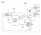
- Fig. 1 shows the configuration of an organic EL lighting apparatus according to a first embodiment.
- Fig. 1 shows the configuration of an organic EL lighting apparatus M1 according to the first embodiment.
- a portion encircled with a chain-dotted line indicates an organic EL element driving device 20.
- Organic EL lighting apparatus M1 includes an organic EL element 2, a power supply 3 and a current control unit 4 connected in series with organic EL element 2, and a voltage control unit 6.
- Organic EL element driving device 20 includes the portion of organic EL lighting apparatus M1 other than organic EL element 2, namely, power supply 3, current control unit 4 and voltage control unit 6.
- Organic EL element driving device 20 drives organic EL element 2 with a constant current.
- Power supply 3 is a variable voltage source capable of varying an output voltage in response to a voltage control signal S4 from voltage control unit 6. That is, power supply 3 is a variable voltage source capable of varying an applied voltage to organic EL element 2.
- Voltage control unit 6 has the function of detecting a voltage across a drain D and a source S of a MOSFET 8 of current control unit 4, and controlling an output voltage from power supply 3. That is, voltage control unit 6 varies an applied voltage from power supply 3 in accordance with luminance control.
- Organic EL element 2 has a structure similar to that illustrated in Fig. 6 .
- organic EL element 2 is represented as a single diode in Fig. 1 , a plurality of organic EL elements may be connected in series. Organic EL element 2 is connected in series between a voltage output terminal of power supply 3 and current control unit 4.
- Current control unit 4 includes a current control circuit 5, a differential amplifier 7, MOSFET 8 and a current detection circuit 9, and has the function of controlling the value of a current passing through organic EL element 2 to a prescribed constant value as will be described later.
- Current detection circuit 9 includes a resistor for detecting the value of a current passing through organic EL element 2, and detects the current value based on a voltage drop that occurs in this resistor.
- current detection circuit 9 includes a plurality of current detection resistors R in parallel for guiding a current passing through organic EL element 2. A voltage drop that occurs in a selected one of the plurality of current detection resistors R is detected, and based on a resistance value of and the voltage drop in the one of current detection resistors R, the value of a current passing through the one of current detection resistors R can be detected.
- Current control circuit 5 controls MOSFET 8 via differential amplifier 7 based on the value of the current passing through organic EL element 2 that has been detected by current detection circuit 9, to control the value of the current passing through organic EL element 2. That is, MOSFET 8 is arranged between organic EL element 2 and current detection circuit 9, and controls the value of the current passing through organic EL element 2.
- the luminance of organic EL element 2 is indicated by a luminance control signal S0 from outside.
- Luminance control signal S0 is input to current control circuit 5.
- the outside refers to a PC (Personal Computer), for example, and luminance control signal S0 is an analog output from a DA (Digital to Analog) terminal provided on the PC. Any device that outputs a signal for controlling luminance other than a PC can be employed.
- Current control circuit 5 determines one of current detection resistors R having an optimal resistance value based on luminance control signal S0, and outputs a resistor switching signal S3 to current detection circuit 9.
- current detection circuit 9 selects the one of current detection resistors R that has been determined by current control circuit 5, and guides the current from organic EL element 2 to the selected one of current detection resistors R.
- current detection circuit 9 when controlling the value of a current passing through organic EL element 2, detects the current value by detecting a voltage drop that occurs in one of current detection resistors R. In detecting the voltage drop in the one of current detection resistors R, a detectable limit of the voltage value, i.e., a detection limit exists.
- the value of a current passing through organic EL element 2 varies significantly as a result of performing the luminance adjustment (dimming) of organic EL element 2.
- the value of the current passing through organic EL element 2 is increased, power consumption in current detection circuit 9, which is wasted without contributing to the luminance of organic EL element 2, is desired to be as low as possible.
- one of current detection resistors R having a higher resistance value is selected to guide the current passing through organic EL element 2 to the one of current detection resistors R.
- one of current detection resistors R having a lower resistance value is selected to guide the current passing through organic EL element 2 to the one of current detection resistors R.
- current control circuit 5 determines a current passing through organic EL element 2 by taking into account operations of all of organic EL element 2, MOSFET 8 and current detection circuit 9 to which a voltage is applied from power supply 3.
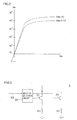
- Fig. 2 is a graph showing current-voltage characteristics of a gate voltage Vgs and a drain D-source S current Ids, with a drain D-source S voltage Vds of MOSFET 8 as a parameter.
- Gate voltage Vgs of MOSFET 8 has a threshold voltage Vth.
- a state where Vds ⁇ Vgs - Vth corresponds to a linear region, and a state where Vds > Vgs - Vth corresponds to a saturation region.
- Ids varies as expressed by equations below for each region.
- Ids K ⁇ ( Vgs - Vth ⁇ Vds - 1 / 2 ⁇ Vds 2
- K represents a constant for each MOSFET.
- Ids Ioled
- MOSFET 8 having the current-voltage characteristics shown in Fig. 2
- drain-source current Ids Ioled such that organic EL element 2 attains a desired luminance can be passed by setting Vds to a minimum value, for example, 0.1 V, and controlling Vgs. While Vds is set to 0.1 V in this embodiment, an optimal value may be set depending on a transistor used.
- current control circuit 5 determines a current value of organic EL element 2 in accordance with luminance control signal S0 indicating a voltage value, determines voltage drop Vs in current detection resistor R at that time as the product of the current value of organic EL element 2 and the resistance value of current detection resistor R, and outputs that voltage drop Vs as a luminance control signal S 1 indicating a voltage value.
- Differential amplifier 7 compares luminance control signal S 1 with a current detection signal S2 indicating a voltage drop in current detection resistor R, and controls gate voltage Vgs of MOSFET 8 such that luminance control signal S 1 becomes equal to current detection signal S2 in voltage. By making the voltage across current detection resistor R equal to S 1 in this manner, the current passing through organic EL element 2 is set to a prescribed value.
- Luminance control signal S 1 may be predetermined based on the luminance-current characteristics of organic EL element 2 and the value of current detection resistor R, stored in a not-shown storage unit, and retrieved from the storage unit by current control unit 4 in response to luminance control signal S0.
- Differential amplifier 7 regulates gate voltage Vgs of MOSFET 8 such that luminance control signal S1 corresponds to current detection signal S2, by raising gate voltage Vgs when current detection signal S2 has a low voltage with respect to luminance control signal S 1, and lowering gate voltage Vgs when current detection signal S2 has a high voltage.
- voltage control unit 6 detects a drain D-source S voltage of MOSFET 8, and outputs voltage control signal S4 to power supply 3 such that this drain D-source S voltage has a value (e.g., 0.1V or 1V) predetermined in accordance with the characteristics of MOSFET 8.
- the specific configuration of voltage control unit 6 may be implemented by the known configuration as disclosed in Japanese Laid-Open Patent Publication No. 2005-033853 or Japanese Laid-Open Patent Publication No. 2008-134288 discussed above.
- the value of the constant current can be varied in accordance with the luminance control by luminance control signal S0.
- Current control unit 4 sets a prescribed value for the current to be passed through organic EL element 2 in accordance with the luminance control by luminance control signal S0, and performs control such that the current passing through organic EL element 2 has the prescribed value in accordance with an output from current detection circuit 9. Furthermore, values of the resistors in current detection circuit 9 are varied in accordance with the luminance control by luminance control signal S0.
- Current control circuit 5 includes a microcontroller with an integral memory, for example, and stores a table from which one of current detection resistors R is selected in accordance with a value of input luminance control signal S0.
- Table 1 illustrates an example of such table.
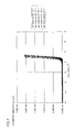
- Fig. 3 is a circuit diagram showing the configuration of current detection circuit 9.
- Current detection circuit 9 includes a plurality of resistors connected in parallel, and switching elements for determining which one of the plurality of resistors receives a current flow.
- current detection circuit 9 includes two current detection resistors R1 an R2 connected in parallel, and MOSFETs 31 and 32 connected in series between organic EL element 2 and current detection resistors R1 an R2, respectively.
- MOSFETs 31 and 32 select one of current detection resistors R1 an R2.
- a resistor selection circuit 33 varies the gate voltages of MOSFETs 31 and 32 in response to resistor switching signal S3 from current control circuit 5, and performs control so that a current passes through one of current detection resistors R1 an R2.
- Resistor selection circuit 33 is a circuit for varying the gate voltages of MOSFETs 31 and 32 and performing output selection (switching), and can be implemented by a known output selection circuit.
- the resistance value is fixed at 1 ⁇ when the current detection resistors are not switched, and a detected voltage varies from 10 mV to 1 V.
- maximum power as high as about 1 W is consumed at the current detection resistor.
- the maximum power consumption is 0.1 W, thereby achieving low power consumption.
- a second embodiment will be described.
- the second embodiment is described particularly with respect to a portion different from that in the first embodiment.
- Fig. 4 shows the configuration of an organic EL lighting apparatus M2 according to the second embodiment.
- a portion encircled with a chain-dotted line indicates an organic EL element driving device 40.
- Organic EL lighting apparatus M2 according to the second embodiment is different from the first embodiment in that two current control circuits 11 and 12 controlled by a current control unit 10 are provided.
- Current control circuit 11 includes a differential amplifier 41, a MOSFET 43 and current detection resistor R1
- current control circuit 12 includes a differential amplifier 42, a MOSFET 44 and current detection resistor R2. While there are two current control circuits in this embodiment, three or more current control circuits may be provided to attain a higher degree of energy savings.
- resistor selection circuit 33 is omitted and one of differential amplifiers 41 and 42 is selected instead by current control unit 10, to select one of current detection resistors R1 and R2 through which a current passes from organic EL element 2. That is, current control unit 10 that has received luminance control signal S0 determines an optimal one of the current detection resistors based on luminance control signal S0, and outputs a voltage to one of the current control circuits having the optimal current detection resistor. A current from organic EL element 2 passes through the selected one of the current control circuits. A voltage is not output to the not-selected one of the current control circuits, and therefore a current from organic EL element 2 does not pass through the not-selected one of the current control circuits.
- Voltage control unit 6 controls power supply 3 by employing a voltage having a smaller potential.
- one of the current control circuits is selected to select one of the current detection resistors.
- the operation subsequent to the resistor selection is similar to that in the first embodiment, and the description thereof is therefore not repeated.
- the current detection resistor itself forms the current detection circuit.
- current control unit 10 includes the plurality of current control circuits 11 and 12 connected in parallel, which include MOSFETs 43 and 44 for controlling the value of a current passing through organic EL element 2, and current detection resistors R1 and R2 connected in series with MOSFETs 43 and 44, respectively.
- Current detection resistors R1 and R2 in the plurality of circuits have resistance values different from each other, and a determination is made about which one of the plurality of current control circuits 11 and 12 receives a current flow.
- a current detection circuit as shown in Fig. 5 can be employed, which includes a plurality of resistors connected in series, and a plurality of switching elements connected in parallel with the plurality of resistors, respectively, for determining which one of the plurality of resistors receives a current flow.
- a current detection circuit 9# includes current detection resistors R1 and R2 connected in series, and MOSFETs 31 and 32 connected in parallel with current detection resistors R1 and R2, respectively.
- Current detection circuit 9# varies the gate voltage of MOSFETs 31 and/or 32, and selectively bypasses one of current detection resistors R1 and R2, to allow a current to pass only through the other resistor.
- selecting either one of two current detection resistors R1 and R2 and selecting both of current detection resistors R1 and R2 can be switched to vary the resistance value.
- Each of the electrical detection circuits shown in Figs. 3 and 5 forms a variable resistor for varying the resistance value of the current detection resistor as necessary.
- the circuit constant of the current detection resistor or the like is variable in accordance with the value of the current. Therefore, an organic EL element driving device capable of attaining a higher degree of energy savings can be provided while a current detection system is maintained.
Landscapes
- Physics & Mathematics (AREA)
- Engineering & Computer Science (AREA)
- Microelectronics & Electronic Packaging (AREA)
- Optics & Photonics (AREA)
- Electroluminescent Light Sources (AREA)
- Control Of El Displays (AREA)
- Circuit Arrangement For Electric Light Sources In General (AREA)
Abstract
Description
- The present invention relates to an organic EL element driving device for driving an organic EL element, and an organic EL lighting apparatus.
- Recent years have seen the acceleration of development of bulb-type fluorescent lamps and bulb-type LED (Light-Emitting Diode) lighting apparatuses which attain a high degree of energy savings in illumination. An organic EL (Electroluminescence) lighting apparatus which attains a similarly high degree of energy savings is a surface-emitting light source, and has advantageous properties of being thin, lightweight and flexible. With such properties, organic EL provides new illumination designs, showcases and showrooms conventionally unattainable, and allows new presentations at a store and the like. The development of organic EL has also been promoted since it is environmentally friendly in that it is mercury-free.
-
Fig. 6 is a schematic diagram showing the cross-sectional structure of a commonorganic EL element 100. As shown inFig. 6 ,organic EL element 100 includes ITO 101, anorganic EL layer 102 and analuminum layer 103, which are stacked on abase member 104.Organic EL element 100 is configured such that a direct-current voltage is applied betweenaluminum layer 103 and ITO 101. - The light emission principle of an organic EL element is to pass a current through an extremely thin film having a transparent conductive film (anode), an organic EL material and a metal electrode (cathode) stacked on a substrate, to produce recoupling of electrons and holes in the organic EL material to thereby generate light.
-
Fig. 7 is a graph showing an example of current-voltage characteristics, which represent a relationship between voltage and current density oforganic EL element 100 for each temperature.Fig. 8 is a graph showing an example of a relationship between current density and luminance oforganic EL element 100 for each temperature. - As shown in
Fig. 7 , the current-voltage characteristics oforganic EL element 100 are similar to the current-voltage characteristics of a diode. Namely, there is very little current flow at a low voltage, and then a current flows abruptly when a certain threshold voltage is reached. Furthermore, as can be seen fromFig. 7 , when the current density is measured with the temperature varying from a room temperature of 26.0 degrees to 81.0 degrees, the threshold voltage is shifted downward as the temperature increases, and when the voltage is constant, the current increases abruptly as the temperature varies. As shown inFig. 8 , on the other hand, the current density and the luminance have an approximately linear relationship, and exhibit relatively stable behavior with respect to temperature. - If
organic EL element 100 exhibiting such behavior is driven by voltage control, a voltage value needs to be controlled with a very high degree of accuracy, and compensation for temperature needs to be made with a similarly high degree of accuracy. Furthermore, iforganic EL element 100 is driven by voltage control, electro-optical conversion efficiency is significantly affected by a variation in threshold voltage during manufacture oforganic EL element 100. For this reason,organic EL element 100 should be driven by current control to obtain a more stable luminance with respect to temperature variation and the like. -
Fig. 9 is a block diagram of a common current driving device for drivingorganic EL element 100.Organic EL element 100 to be driven, apower supply 202 and acurrent control unit 203 are connected in series.Current control unit 203 includes a MOSFET (Metal Oxide Semiconductor Field Effect Transistor) 205, acurrent control circuit 204 and acurrent detection resistor 201. -
Current control unit 203 measures a voltage Vs acrosscurrent detection resistor 201 having a resistance value Rs, in order to pass a constant current Ioled throughorganic EL element 100 by usingcurrent control circuit 204.Current control unit 203 compares measured voltage Vs with a reference voltage Vref, and controls a gate voltage ofMOSFET 205 in response to a signal from the current control circuit to satisfy voltage Vs = reference voltage Vref, to vary a current passing throughMOSFET 205. When Vref = Vs is satisfied, current Ioled passing throughorganic EL element 100 is obtained by an equation below.
- As can be seen from this equation, current Ioled can be varied by varying the value of Vref.
- A voltage Vo supplied to
organic EL element 100 frompower supply 202 is the sum of a voltage drop Voled inorganic EL element 100, a voltage drop Vmos inMOSFET 205, and a voltage drop Vs incurrent detection resistor 201. In reality, voltage Vo needs to be set to a sufficiently large value by taking into account a margin to adapt to the adjustment of luminance oforganic EL element 100, a variation during a manufacturing stage, temperature characteristics, temporal variation and the like oforganic EL element 100. - Power based on the voltage set to a sufficiently large value with a margin, however, becomes heat at
MOSFET 205 and/orcurrent detection resistor 201 and is consumed. That is, power based on this extra voltage is wasted without contributing to light emission. - In particular, when luminance adjustment for
organic EL element 100, i.e., dimming needs to be performed, an approximately double-digit dimming range is required, which requires a double-digit range for current. During dimming, therefore, a voltage detected bycurrent detection resistor 201 varies in double digits. Since power consumption is proportional to the square of voltage, double-digit variation in voltage causes four-digit variation in power, resulting in power wasted particularly in a low luminance region. - PTL 1 discloses a driving device including a group of a plurality of light-emitting elements (light-emitting diodes) connected to a plurality of constant current supplies, respectively, in which switching control of a power supply circuit is performed such that the lowest one of dropped voltages of the constant current supplies is constant. It is stated that, according to this technique of controlling the dropped voltage of the constant current supply to a constant value, a loss in voltage detection by detecting the resistance is not increased even if a current passing through the light-emitting diodes increases.
- Japanese Laid-Open Patent Publication No.
2008-134288 -
PTL 1: Japanese Laid-Open Patent Publication No. 2005-033853 PTL 2: Japanese Laid-Open Patent Publication No. 2008-134288 - In the techniques described in
PTLs 1 and 2, however, a circuit constant of the resistor and the like in the current control unit described above is considered to be not variable but set to a constant value. Accordingly, when a current detection resistor adaptable to a low luminance region is used, power consumption is wasted in the current control unit in a high luminance region. - In view of the above, the present invention provides an organic EL element driving device and an organic EL lighting apparatus capable of achieving more energy savings than conventional technique.
- According to an aspect of the present invention, an organic EL element driving device that drives an organic EL element with a constant current and is capable of varying a value of the constant current in accordance with luminance control is provided. The organic EL element driving device includes a power supply connected in series with the organic EL element, and a current control unit connected in series with the organic EL element. The current control unit includes a current detection circuit having a resistor for detecting the value of the current passing through the organic EL element. The current control unit sets a prescribed value for the current to be passed through the organic EL element in accordance with the luminance control, and performs control such that the current passing through the organic EL element has the prescribed value in accordance with an output from the current detection circuit. A value of the resistor in the current detection circuit is varied in accordance with the luminance control.
- An organic EL lighting apparatus according to another aspect of the present invention includes an organic EL element, and an organic EL element driving device that drives the organic EL element with a constant current and is capable of varying a value of the constant current in accordance with luminance control. The organic EL element driving device includes a power supply connected in series with the organic EL element, and a current control unit connected in series with the organic EL element. The current control unit includes a current detection circuit having a resistor for detecting the value of the current passing through the organic EL element. The current control unit sets a prescribed value for the current to be passed through the organic EL element in accordance with the luminance control, and performs control such that the current passing through the organic EL element has the prescribed value in accordance with an output from the current detection circuit. A value of the resistor in the current detection circuit is varied in accordance with the luminance control.
- According to the present invention, an organic EL element driving device and an organic EL lighting apparatus capable of achieving more energy savings than conventional technique can be provided.
-
Fig. 1 shows the configuration of an organic EL lighting apparatus according to a first embodiment. -
Fig. 2 is a graph showing current-voltage characteristics of a gate voltage Vgs and a drain-source current Ids, with a drain-source voltage Vds of a MOSFET as a parameter. -
Fig. 3 is a circuit diagram showing the configuration of a current detection circuit. -
Fig. 4 shows the configuration of an organic EL lighting apparatus according to a second embodiment. -
Fig. 5 is a circuit diagram showing another configuration of the current detection circuit. -
Fig. 6 is a schematic diagram showing the cross-sectional structure of a common organic EL element. -
Fig. 7 is a graph showing an example of current-voltage characteristics, which represent a relationship between voltage and current density of the organic EL element for each temperature. -
Fig. 8 is a graph showing an example of a relationship between current density and luminance of the organic EL element for each temperature. -
Fig. 9 is a block diagram of a common current driving device for driving the organic EL element. - A first embodiment of the present invention will be described with reference to the drawings. The present invention, however, is not limited to the embodiments described below.
-
Fig. 1 shows the configuration of an organic EL lighting apparatus M1 according to the first embodiment. In this figure, a portion encircled with a chain-dotted line indicates an organic ELelement driving device 20. - Organic EL lighting apparatus M1 includes an
organic EL element 2, apower supply 3 and acurrent control unit 4 connected in series withorganic EL element 2, and avoltage control unit 6. Organic ELelement driving device 20 includes the portion of organic EL lighting apparatus M1 other thanorganic EL element 2, namely,power supply 3,current control unit 4 andvoltage control unit 6. Organic ELelement driving device 20 drivesorganic EL element 2 with a constant current. -
Power supply 3 is a variable voltage source capable of varying an output voltage in response to a voltage control signal S4 fromvoltage control unit 6. That is,power supply 3 is a variable voltage source capable of varying an applied voltage toorganic EL element 2.Voltage control unit 6 has the function of detecting a voltage across a drain D and a source S of aMOSFET 8 ofcurrent control unit 4, and controlling an output voltage frompower supply 3. That is,voltage control unit 6 varies an applied voltage frompower supply 3 in accordance with luminance control. -
Organic EL element 2 has a structure similar to that illustrated inFig. 6 . - While
organic EL element 2 is represented as a single diode inFig. 1 , a plurality of organic EL elements may be connected in series.Organic EL element 2 is connected in series between a voltage output terminal ofpower supply 3 andcurrent control unit 4. -
Current control unit 4 includes a current control circuit 5, adifferential amplifier 7,MOSFET 8 and acurrent detection circuit 9, and has the function of controlling the value of a current passing throughorganic EL element 2 to a prescribed constant value as will be described later. -
Current detection circuit 9 includes a resistor for detecting the value of a current passing throughorganic EL element 2, and detects the current value based on a voltage drop that occurs in this resistor. Specifically,current detection circuit 9 includes a plurality of current detection resistors R in parallel for guiding a current passing throughorganic EL element 2. A voltage drop that occurs in a selected one of the plurality of current detection resistors R is detected, and based on a resistance value of and the voltage drop in the one of current detection resistors R, the value of a current passing through the one of current detection resistors R can be detected. - Current control circuit 5
controls MOSFET 8 viadifferential amplifier 7 based on the value of the current passing throughorganic EL element 2 that has been detected bycurrent detection circuit 9, to control the value of the current passing throughorganic EL element 2. That is,MOSFET 8 is arranged betweenorganic EL element 2 andcurrent detection circuit 9, and controls the value of the current passing throughorganic EL element 2. - The luminance of
organic EL element 2 is indicated by a luminance control signal S0 from outside. Luminance control signal S0 is input to current control circuit 5. The outside as used herein refers to a PC (Personal Computer), for example, and luminance control signal S0 is an analog output from a DA (Digital to Analog) terminal provided on the PC. Any device that outputs a signal for controlling luminance other than a PC can be employed. - Current control circuit 5 determines one of current detection resistors R having an optimal resistance value based on luminance control signal S0, and outputs a resistor switching signal S3 to
current detection circuit 9. In response to resistor switching signal S3,current detection circuit 9 selects the one of current detection resistors R that has been determined by current control circuit 5, and guides the current fromorganic EL element 2 to the selected one of current detection resistors R. - In this embodiment, when controlling the value of a current passing through
organic EL element 2,current detection circuit 9 detects the current value by detecting a voltage drop that occurs in one of current detection resistors R. In detecting the voltage drop in the one of current detection resistors R, a detectable limit of the voltage value, i.e., a detection limit exists. - In this embodiment, on the other hand, the value of a current passing through
organic EL element 2 varies significantly as a result of performing the luminance adjustment (dimming) oforganic EL element 2. In particular, if the value of the current passing throughorganic EL element 2 is increased, power consumption incurrent detection circuit 9, which is wasted without contributing to the luminance oforganic EL element 2, is desired to be as low as possible. - Accordingly, if a voltage drop in current detection resistor R through which the current of
organic EL element 2 passes is great as compared to the detection limit of voltage value, the voltage drop in current detection resistor R can be detected adequately. Therefore, the resistance value of current detection resistor R is desired to be smaller. - In this embodiment, therefore, when a current passing through
organic EL element 2 has a small value, one of current detection resistors R having a higher resistance value is selected to guide the current passing throughorganic EL element 2 to the one of current detection resistors R. When a current passing throughorganic EL element 2 has a large value, one of current detection resistors R having a lower resistance value is selected to guide the current passing throughorganic EL element 2 to the one of current detection resistors R. As a result, a voltage drop larger than the detection limit of voltage value is secured, while power consumed in the one of current detection resistors R is reduced. - When adjusting the luminance of
organic EL element 2, current control circuit 5 determines a current passing throughorganic EL element 2 by taking into account operations of all oforganic EL element 2,MOSFET 8 andcurrent detection circuit 9 to which a voltage is applied frompower supply 3. - The current passing through
organic EL element 2 is determined by controllingMOSFET 8.Fig. 2 is a graph showing current-voltage characteristics of a gate voltage Vgs and a drain D-source S current Ids, with a drain D-source S voltage Vds ofMOSFET 8 as a parameter. - Gate voltage Vgs of
MOSFET 8 has a threshold voltage Vth. A state where Vds < Vgs - Vth corresponds to a linear region, and a state where Vds > = Vgs - Vth corresponds to a saturation region. Ids varies as expressed by equations below for each region.


- Here, K represents a constant for each MOSFET. In order to minimize power consumption in
MOSFET 8, each of Vds and Ids needs to be reduced. Since Ids is equal to Ioled, forMOSFET 8 having the current-voltage characteristics shown inFig. 2 , drain-source current Ids = Ioled such thatorganic EL element 2 attains a desired luminance can be passed by setting Vds to a minimum value, for example, 0.1 V, and controlling Vgs. While Vds is set to 0.1 V in this embodiment, an optimal value may be set depending on a transistor used. - To set Vgs of
MOSFET 8 to the value thus determined, overall control is performed by taking into account how voltage Vo supplied toorganic EL element 2 frompower supply 3 is allocated among voltage drop Voled inorganic EL element 2, voltage drop Vmos inMOSFET 8, and voltage drop Vs in current detection resistor R. - Specifically, current control circuit 5 determines a current value of
organic EL element 2 in accordance with luminance control signal S0 indicating a voltage value, determines voltage drop Vs in current detection resistor R at that time as the product of the current value oforganic EL element 2 and the resistance value of current detection resistor R, and outputs that voltage drop Vs as a luminance control signal S 1 indicating a voltage value. -
Differential amplifier 7 compares luminance control signal S 1 with a current detection signal S2 indicating a voltage drop in current detection resistor R, and controls gate voltage Vgs ofMOSFET 8 such that luminance control signal S 1 becomes equal to current detection signal S2 in voltage. By making the voltage across current detection resistor R equal to S 1 in this manner, the current passing throughorganic EL element 2 is set to a prescribed value. Luminance control signal S 1 may be predetermined based on the luminance-current characteristics oforganic EL element 2 and the value of current detection resistor R, stored in a not-shown storage unit, and retrieved from the storage unit bycurrent control unit 4 in response to luminance control signal S0. -
Differential amplifier 7 regulates gate voltage Vgs ofMOSFET 8 such that luminance control signal S1 corresponds to current detection signal S2, by raising gate voltage Vgs when current detection signal S2 has a low voltage with respect to luminance control signal S 1, and lowering gate voltage Vgs when current detection signal S2 has a high voltage. In parallel with this operation,voltage control unit 6 detects a drain D-source S voltage ofMOSFET 8, and outputs voltage control signal S4 topower supply 3 such that this drain D-source S voltage has a value (e.g., 0.1V or 1V) predetermined in accordance with the characteristics ofMOSFET 8. The specific configuration ofvoltage control unit 6 may be implemented by the known configuration as disclosed in Japanese Laid-Open Patent Publication No.2005-033853 2008-134288 - That is, in organic EL
element driving device 20, the value of the constant current can be varied in accordance with the luminance control by luminance control signal S0.Current control unit 4 sets a prescribed value for the current to be passed throughorganic EL element 2 in accordance with the luminance control by luminance control signal S0, and performs control such that the current passing throughorganic EL element 2 has the prescribed value in accordance with an output fromcurrent detection circuit 9. Furthermore, values of the resistors incurrent detection circuit 9 are varied in accordance with the luminance control by luminance control signal S0. - By performing the control as described above, power consumed in
current control unit 4 can be minimized while the accuracy of current detection in the current detection resistor is maintained. - Next, current control circuit 5 and
current detection circuit 9 will be described in detail. Current control circuit 5 includes a microcontroller with an integral memory, for example, and stores a table from which one of current detection resistors R is selected in accordance with a value of input luminance control signal S0. Table 1 illustrates an example of such table.[Table 1] Luminance signal relative value Resistance value (Ω) Voltage range (V) Current range (A) 0∼10 1 0.01∼0.1 0.01∼0.1 10∼100 0.1 0.01∼0.1 0.1∼1 -
Fig. 3 is a circuit diagram showing the configuration ofcurrent detection circuit 9.Current detection circuit 9 includes a plurality of resistors connected in parallel, and switching elements for determining which one of the plurality of resistors receives a current flow. Specifically,current detection circuit 9 includes two current detection resistors R1 an R2 connected in parallel, andMOSFETs organic EL element 2 and current detection resistors R1 an R2, respectively.MOSFETs resistor selection circuit 33 varies the gate voltages ofMOSFETs organic EL element 2 passes as a drain D-source S current ofMOSFET Resistor selection circuit 33 is a circuit for varying the gate voltages ofMOSFETs - While the two current detection resistors are switched for use in
current detection circuit 9 in this embodiment, three or more current detection resistors can be switched for use to attain a higher degree of energy savings. Moreover, while either one of two current detection resistors R1 an R2 is selected in the configuration described above, both of current detection resistors R1 an R2 can be selected and their combined resistance can be used to vary the resistance value. - In this embodiment, if the range of variation in current value is set from 10 to 1000 mA and the lowest accuracy for current detection signal S2 is set to 10 mV, for example, the resistance value is fixed at 1 Ω when the current detection resistors are not switched, and a detected voltage varies from 10 mV to 1 V. In this case, maximum power as high as about 1 W is consumed at the current detection resistor. This is a very large value with respect to power of about 3.5W which is consumed by
organic EL element 2. In this embodiment, on the other hand, the range of variation in current value is set to 10 to 100 and 100 to 1000 where R1 = 1 Ω and R2 = 0.1 Ω are switched from each other, respectively, and current detection signal S2 of 10 to 100 mV is used. As such, the maximum power consumption is 0.1 W, thereby achieving low power consumption. - A second embodiment will be described. The second embodiment is described particularly with respect to a portion different from that in the first embodiment.
-
Fig. 4 shows the configuration of an organic EL lighting apparatus M2 according to the second embodiment. In this figure, a portion encircled with a chain-dotted line indicates an organic ELelement driving device 40. - Organic EL lighting apparatus M2 according to the second embodiment is different from the first embodiment in that two
current control circuits current control unit 10 are provided. -
Current control circuit 11 includes adifferential amplifier 41, aMOSFET 43 and current detection resistor R1, andcurrent control circuit 12 includes adifferential amplifier 42, aMOSFET 44 and current detection resistor R2. While there are two current control circuits in this embodiment, three or more current control circuits may be provided to attain a higher degree of energy savings. - While current detection resistors R1 and R2 are switched by
resistor selection circuit 33 in the first embodiment, the differential amplifier, the MOSFET and the current detection resistor are switched together in the second embodiment. In this case,resistor selection circuit 33 is omitted and one ofdifferential amplifiers current control unit 10, to select one of current detection resistors R1 and R2 through which a current passes fromorganic EL element 2. That is,current control unit 10 that has received luminance control signal S0 determines an optimal one of the current detection resistors based on luminance control signal S0, and outputs a voltage to one of the current control circuits having the optimal current detection resistor. A current fromorganic EL element 2 passes through the selected one of the current control circuits. A voltage is not output to the not-selected one of the current control circuits, and therefore a current fromorganic EL element 2 does not pass through the not-selected one of the current control circuits. -
Voltage control unit 6 controlspower supply 3 by employing a voltage having a smaller potential. - Thus, in the second embodiment, one of the current control circuits is selected to select one of the current detection resistors. The operation subsequent to the resistor selection is similar to that in the first embodiment, and the description thereof is therefore not repeated. In the second embodiment, the current detection resistor itself forms the current detection circuit.
- Thus,
current control unit 10 includes the plurality ofcurrent control circuits MOSFETs organic EL element 2, and current detection resistors R1 and R2 connected in series withMOSFETs current control circuits - Other than the circuit shown in
Fig. 3 , a current detection circuit as shown inFig. 5 can be employed, which includes a plurality of resistors connected in series, and a plurality of switching elements connected in parallel with the plurality of resistors, respectively, for determining which one of the plurality of resistors receives a current flow. Specifically, acurrent detection circuit 9# includes current detection resistors R1 and R2 connected in series, andMOSFETs Current detection circuit 9# varies the gate voltage ofMOSFETs 31 and/or 32, and selectively bypasses one of current detection resistors R1 and R2, to allow a current to pass only through the other resistor. Alternatively, selecting either one of two current detection resistors R1 and R2 and selecting both of current detection resistors R1 and R2 can be switched to vary the resistance value. - Each of the electrical detection circuits shown in
Figs. 3 and5 forms a variable resistor for varying the resistance value of the current detection resistor as necessary. - As described above, according to the embodiments discussed above, when controlling the value of the current passing through the organic EL element, the circuit constant of the current detection resistor or the like is variable in accordance with the value of the current. Therefore, an organic EL element driving device capable of attaining a higher degree of energy savings can be provided while a current detection system is maintained.
- It should be understood that the embodiments disclosed herein are illustrative and non-restrictive in every respect. The scope of the present invention is defined by the terms of the claims, rather than the description above, and is intended to include any modifications within the scope and meaning equivalent to the terms of the claims.
- 2, 100 organic EL element; 3, 202 power supply; 4, 10, 203 current control unit; 5, 11, 12, 204 current control circuit; 6 voltage control unit; 7, 41, 42 differential amplifier; 8, 31, 43, 44, 205 MOSFET; 9, 9# current detection circuit; 20, 40 organic EL element driving device; 33 resistor selection circuit; 101 ITO; 102 organic EL layer; 103 aluminum layer; 104 base member; 201, R, R2 current detection resistor; M1, M2 organic EL lighting apparatus.
Claims (7)
- An organic EL element driving device (20, 40) that drives an organic EL element (2) with a constant current and is capable of varying a value of the constant current in accordance with luminance control, comprising:a power supply (3) connected in series with said organic EL element; anda current control unit (4, 10) connected in series with said organic EL element, whereinsaid current control unit includes a current detection circuit (9) having a resistor for detecting the value of the current passing through said organic EL element,said current control unit sets a prescribed value for the current to be passed through said organic EL element in accordance with said luminance control, and performs control such that the current passing through said organic EL element has said prescribed value in accordance with an output from said current detection circuit, anda value of the resistor in said current detection circuit is varied in accordance with said luminance control.
- The organic EL element driving device according to claim 1, wherein
said power supply is a variable voltage source capable of varying an applied voltage, and
said driving device further comprises a voltage control unit for varying the applied voltage from said voltage source in accordance with said luminance control. - The organic EL element driving device according to claim 1, wherein
said current control unit includes a MOSFET arranged between said organic EL element and said current detection circuit, for controlling the value of the current passing through said organic EL element. - The organic EL element driving device according to any one of claims 1 to 3, wherein
said current detection circuit includes a plurality of resistors connected in parallel, and a switching element for determining which one of the plurality of resistors receives a current flow. - The organic EL element driving device according to any one of claims 1 to 3, wherein
said current detection circuit includes a plurality of resistors connected in series, and a plurality of switching elements connected in parallel with said plurality of resistors, respectively, for determining which one of the plurality of resistors receives a current flow. - The organic EL element driving device according to claim 1 or 2, wherein said current control unit includes a plurality of current control circuits connected in parallel,
each of said plurality of current control circuits includes a MOSFET for controlling the value of the current passing through said organic EL element, and a resistor connected in series with the MOSFET,
the resistors in said plurality of current control circuits have resistance values different from each other, and
a determination is made about which one of said plurality of current control circuits receives a current flow. - An organic EL lighting apparatus (M1, M2) comprising:an organic EL element (2); andan organic EL element driving device (20, 40) that drives said organic EL element with a constant current and is capable of varying a value of the constant current in accordance with luminance control,said organic EL element driving device includinga power supply (3) connected in series with said organic EL element, anda current control unit (4, 10) connected in series with said organic EL element, whereinsaid current control unit includes a current detection circuit (9) having a resistor for detecting the value of the current passing through said organic EL element,said current control unit sets a prescribed value for the current to be passed through said organic EL element in accordance with said luminance control, and performs control such that the current passing through said organic EL element has said prescribed value in accordance with an output from said current detection circuit, anda value of the resistor in said current detection circuit is varied in accordance with said luminance control.
Applications Claiming Priority (2)
| Application Number | Priority Date | Filing Date | Title |
|---|---|---|---|
| JP2010139127 | 2010-06-18 | ||
| PCT/JP2011/063495 WO2011158786A1 (en) | 2010-06-18 | 2011-06-13 | Drive device for organic el element, and organic el illumination device |
Publications (2)
| Publication Number | Publication Date |
|---|---|
| EP2584871A1 true EP2584871A1 (en) | 2013-04-24 |
| EP2584871A4 EP2584871A4 (en) | 2017-06-21 |
Family
ID=45348185
Family Applications (1)
| Application Number | Title | Priority Date | Filing Date |
|---|---|---|---|
| EP11795692.0A Withdrawn EP2584871A4 (en) | 2010-06-18 | 2011-06-13 | Drive device for organic el element, and organic el illumination device |
Country Status (4)
| Country | Link |
|---|---|
| US (1) | US9497805B2 (en) |
| EP (1) | EP2584871A4 (en) |
| JP (1) | JP4973814B2 (en) |
| WO (1) | WO2011158786A1 (en) |
Cited By (1)
| Publication number | Priority date | Publication date | Assignee | Title |
|---|---|---|---|---|
| CN104320888A (en) * | 2014-11-07 | 2015-01-28 | 广西大学 | Timed sound control lamp |
Families Citing this family (10)
| Publication number | Priority date | Publication date | Assignee | Title |
|---|---|---|---|---|
| JP2015088386A (en) * | 2013-10-31 | 2015-05-07 | ミネベア株式会社 | LED driving device and lighting apparatus |
| WO2015178336A1 (en) * | 2014-05-21 | 2015-11-26 | コニカミノルタ株式会社 | Lighting device |
| JP6495670B2 (en) * | 2015-01-28 | 2019-04-03 | 新日本無線株式会社 | LED drive circuit |
| US10542593B1 (en) * | 2019-01-18 | 2020-01-21 | Infineon Technologies Ag | Power offloading for linear current source |
| JP7265419B2 (en) * | 2019-06-05 | 2023-04-26 | ローム株式会社 | Light-emitting element driving device |
| JP7398091B2 (en) * | 2019-11-28 | 2023-12-14 | 株式会社共進電機製作所 | lighting device |
| JP7208186B2 (en) * | 2020-03-06 | 2023-01-18 | 矢崎総業株式会社 | switch module |
| KR102253416B1 (en) | 2020-06-10 | 2021-05-18 | 주식회사 동운아나텍 | Current driving circuit |
| US11849514B1 (en) | 2022-06-10 | 2023-12-19 | Infineon Technologies Ag | Current regulator circuits with self-adaptive power offloading |
| US12464619B2 (en) | 2023-05-02 | 2025-11-04 | Infineon Technologies Ag | Light emitting diode (LED) current regulator circuit with multiple LED pins for robust control of LED chain |
Family Cites Families (18)
| Publication number | Priority date | Publication date | Assignee | Title |
|---|---|---|---|---|
| DE602004008840T2 (en) | 2003-07-07 | 2008-06-19 | Rohm Co., Ltd., Kyoto | A load driving device and portable device using such load driving device |
| JP3755770B2 (en) | 2003-07-07 | 2006-03-15 | ローム株式会社 | Load drive device and portable device |
| JP2005078828A (en) * | 2003-08-28 | 2005-03-24 | Konica Minolta Holdings Inc | Illumination device and driving method of illumination device |
| JP4246029B2 (en) | 2003-10-07 | 2009-04-02 | 財団法人21あおもり産業総合支援センター | LED driving circuit and power saving method thereof |
| JP2006121774A (en) | 2004-10-19 | 2006-05-11 | Denso Corp | Motor control circuit |
| JP3904579B2 (en) * | 2004-12-03 | 2007-04-11 | ローム株式会社 | Power supply device, light emitting device using the same, and electronic device |
| JP2006303002A (en) | 2005-04-18 | 2006-11-02 | Toshiba Corp | Information processing apparatus and brightness adjustment method |
| JP2007280559A (en) | 2006-04-11 | 2007-10-25 | Matsushita Electric Ind Co Ltd | Optical pickup device |
| WO2008050679A1 (en) * | 2006-10-25 | 2008-05-02 | Panasonic Electric Works Co., Ltd. | Led lighting circuit and illuminating apparatus using the same |
| JP2008134288A (en) | 2006-11-27 | 2008-06-12 | Sharp Corp | LED driver |
| TWI362639B (en) * | 2007-01-31 | 2012-04-21 | Richtek Technology Corp | Backlight control circuit with flexible configuration |
| US8508464B2 (en) * | 2007-01-31 | 2013-08-13 | Richtek Technology Corporation | Backlight control circuit capable of distinguishing under current condition |
| JP5024789B2 (en) * | 2007-07-06 | 2012-09-12 | Nltテクノロジー株式会社 | Light emission control circuit, light emission control method, surface illumination device, and liquid crystal display device including the surface illumination device |
| JP2009026544A (en) * | 2007-07-18 | 2009-02-05 | Showa Denko Kk | LED dimming device and LED lighting device |
| JP2009261213A (en) * | 2008-03-24 | 2009-11-05 | Toshiba Lighting & Technology Corp | Power supply apparatus and luminaire |
| US20100283773A1 (en) * | 2009-05-08 | 2010-11-11 | Yong-Hun Kim | Driving integrated circuit and image display device including the same |
| TWI415518B (en) * | 2009-06-02 | 2013-11-11 | Richtek Technology Corp | Light emitting device driver circuit, light emitting device array controller and control method thereof |
| TW201044915A (en) * | 2009-06-03 | 2010-12-16 | Richtek Technology Corp | AC power line controlled light emitting device dimming circuit and method thereof |
-
2011
- 2011-06-13 US US13/703,088 patent/US9497805B2/en not_active Expired - Fee Related
- 2011-06-13 WO PCT/JP2011/063495 patent/WO2011158786A1/en not_active Ceased
- 2011-06-13 JP JP2011548482A patent/JP4973814B2/en not_active Expired - Fee Related
- 2011-06-13 EP EP11795692.0A patent/EP2584871A4/en not_active Withdrawn
Non-Patent Citations (1)
| Title |
|---|
| See references of WO2011158786A1 * |
Cited By (1)
| Publication number | Priority date | Publication date | Assignee | Title |
|---|---|---|---|---|
| CN104320888A (en) * | 2014-11-07 | 2015-01-28 | 广西大学 | Timed sound control lamp |
Also Published As
| Publication number | Publication date |
|---|---|
| EP2584871A4 (en) | 2017-06-21 |
| WO2011158786A1 (en) | 2011-12-22 |
| US20130088174A1 (en) | 2013-04-11 |
| US9497805B2 (en) | 2016-11-15 |
| JPWO2011158786A1 (en) | 2013-08-19 |
| JP4973814B2 (en) | 2012-07-11 |
Similar Documents
| Publication | Publication Date | Title |
|---|---|---|
| EP2584871A1 (en) | Drive device for organic el element, and organic el illumination device | |
| JP5120876B2 (en) | Organic electroluminescent display device and driving method thereof | |
| JP4972068B2 (en) | Driving device for light emitting element | |
| TWI522011B (en) | Adaptive switching mode LED driver | |
| US8258711B2 (en) | Semiconductor device, LED driving circuit, and apparatus for displaying an image | |
| JP5592434B2 (en) | Power supply device, display device including the same, and driving method thereof | |
| JP5004700B2 (en) | Light emitting element driving device | |
| JP4822387B2 (en) | Drive device for organic EL panel | |
| US20100177127A1 (en) | Led driving circuit, semiconductor element and image display device | |
| US8288960B2 (en) | Two-terminal current controller and related LED lighting device | |
| TW201408127A (en) | Light emitting diode driving apparatus | |
| CN101014989A (en) | Driver for OLED passive matrix display | |
| JP5275134B2 (en) | LED drive circuit | |
| JP2006220851A (en) | Driving mechanism of light emitting display panel and driving method | |
| US8729822B2 (en) | LED emitting device and driving method thereof | |
| US8803430B2 (en) | Light source module, method of driving the light source module and display apparatus having the light source module | |
| JP4539963B2 (en) | Active drive type light emitting display device and electronic device equipped with the display device | |
| US7812834B2 (en) | DC stabilization circuit for organic electroluminescent display device and power supply using the same | |
| US8674609B2 (en) | Two-terminal current controller and related LED lighting device | |
| KR102863468B1 (en) | Apparatus of driving a light source and method thereof | |
| CN119729948A (en) | Multi-channel independently adjustable OLED constant current driver and OLED constant current driving method | |
| JP5771450B2 (en) | LIGHT EMITTING DIODE DRIVING CIRCUIT AND LIGHT EMITTING DEVICE AND ELECTRONIC DEVICE USING THE SAME | |
| CN119893786A (en) | Single-path adjustable OLED constant current driver and OLED constant current driving method | |
| JP2005003837A (en) | Driving device of light emitting display panel and driving method |
Legal Events
| Date | Code | Title | Description |
|---|---|---|---|
| PUAI | Public reference made under article 153(3) epc to a published international application that has entered the european phase |
Free format text: ORIGINAL CODE: 0009012 |
|
| 17P | Request for examination filed |
Effective date: 20121213 |
|
| AK | Designated contracting states |
Kind code of ref document: A1 Designated state(s): AL AT BE BG CH CY CZ DE DK EE ES FI FR GB GR HR HU IE IS IT LI LT LU LV MC MK MT NL NO PL PT RO RS SE SI SK SM TR |
|
| DAX | Request for extension of the european patent (deleted) | ||
| RA4 | Supplementary search report drawn up and despatched (corrected) |
Effective date: 20170523 |
|
| RIC1 | Information provided on ipc code assigned before grant |
Ipc: H05B 37/02 20060101AFI20170517BHEP Ipc: H05B 33/08 20060101ALI20170517BHEP Ipc: H01L 51/50 20060101ALI20170517BHEP |
|
| STAA | Information on the status of an ep patent application or granted ep patent |
Free format text: STATUS: THE APPLICATION HAS BEEN WITHDRAWN |
|
| 18W | Application withdrawn |
Effective date: 20190219 |