EP2584183A1 - Electrical Drive Arrangement for a Fuel Injection System - Google Patents
Electrical Drive Arrangement for a Fuel Injection System Download PDFInfo
- Publication number
- EP2584183A1 EP2584183A1 EP12195288.1A EP12195288A EP2584183A1 EP 2584183 A1 EP2584183 A1 EP 2584183A1 EP 12195288 A EP12195288 A EP 12195288A EP 2584183 A1 EP2584183 A1 EP 2584183A1
- Authority
- EP
- European Patent Office
- Prior art keywords
- voltage
- terminal
- effect transistor
- field effect
- regulation device
- Prior art date
- Legal status (The legal status is an assumption and is not a legal conclusion. Google has not performed a legal analysis and makes no representation as to the accuracy of the status listed.)
- Granted
Links
Images



Classifications
-
- F—MECHANICAL ENGINEERING; LIGHTING; HEATING; WEAPONS; BLASTING
- F02—COMBUSTION ENGINES; HOT-GAS OR COMBUSTION-PRODUCT ENGINE PLANTS
- F02D—CONTROLLING COMBUSTION ENGINES
- F02D41/00—Electrical control of supply of combustible mixture or its constituents
- F02D41/20—Output circuits, e.g. for controlling currents in command coils
- F02D41/2096—Output circuits, e.g. for controlling currents in command coils for controlling piezoelectric injectors
-
- F—MECHANICAL ENGINEERING; LIGHTING; HEATING; WEAPONS; BLASTING
- F02—COMBUSTION ENGINES; HOT-GAS OR COMBUSTION-PRODUCT ENGINE PLANTS
- F02D—CONTROLLING COMBUSTION ENGINES
- F02D41/00—Electrical control of supply of combustible mixture or its constituents
- F02D41/20—Output circuits, e.g. for controlling currents in command coils
- F02D2041/202—Output circuits, e.g. for controlling currents in command coils characterised by the control of the circuit
- F02D2041/2051—Output circuits, e.g. for controlling currents in command coils characterised by the control of the circuit using voltage control
Definitions
- the present invention relates to an automotive fuel injection system and, more particularly, to an electrical drive arrangement for use in such a fuel injection system.
- Modern automotive vehicle engines are generally equipped with fuel injectors for injecting fuel (e.g. gasoline or diesel fuel) into the individual cylinders of the engine.
- the fuel injectors are coupled to a source of high pressure fuel that is delivered to the injectors by way of a fuel delivery system.
- the fuel injectors typically employ a valve needle that is actuated to disengage and re-engage an associated valve seat so as to control the amount of high pressure fuel that is metered from the fuel delivery system and injected into a corresponding engine cylinder.
- solenoid operated injectors in which an electrically driven solenoid is operably connected to the valve needle. Energising the solenoid causes the valve needle to disengage from its seat, thus permitting fuel delivery, and de-energising the solenoid causes the valve needle to re-engage it seat, thus preventing fuel delivery.
- FIG. 1 shows a simplified schematic of a known drive arrangement 2 which includes an injector driver stage 4 that is supplied with power from a vehicle power supply 6, typically the vehicle battery, and provides power and control inputs to one or more fuel injectors 8 (two of which are shown in Figure 1 ).
- a vehicle power supply 6 typically the vehicle battery
- the injector driver stage 4 is a circuit arrangement that is configured to select a specific one of the injectors 8 for operation and to apply an operating voltage thereto.
- the functionality of the injector driver stage 4 is controlled by an Engine Control Unit 10 (ECU) of the vehicle within which it is installed.
- ECU Engine Control Unit 10
- a known problem is that such electrical drive arrangements do not operate under ideal conditions and are typically supplied with electrical power that is subject to spurious electrical oscillations, hereinafter referred to as 'noise'.
- a significant proportion of power supply noise can be compensated for by the injector drive stage 4 under the control of the ECU 10 since some sources of noise are predictable. However, some sources of noise are not predictable and such noise affects detrimentally the level of control that the ECU 10 has over the operational timing of the injectors 8.
- the invention provides an electrical drive arrangement of a fuel injection system comprising a power supply operatively connected to an injector driver stage which, in turn, is operatively connected to at least one fuel injector, and a voltage regulation device comprising an input terminal connected to the power supply and an output terminal connected to the injector driver stage and a field effect transistor including a drain terminal connected to the input terminal of the voltage regulation device, a source terminal connected to the output terminal of the voltage regulation device and a gate terminal.
- the filter device is operatively connected between the gate terminal of the field effect transistor and the input terminal of the voltage regulation device, thereby supplying a filtered voltage from the power supply as an input to the gate terminal.
- the filter device includes: i) a resistor element connected between the gate terminal and the input terminal; and ii) a capacitor element connected between the gate terminal and an electrical ground connection.
- a current sense element is connected between the capacitor element and the electrical ground connection, and a feedback path is connected therebetween to provide an injector voltage signal to the gate terminal of the voltage regulation device.
- This configuration provides the benefit that the voltage at the gate terminal of the field effect transistor is modified as a function of the load on the injector driver stage which adjusts the conductivity of the transistor thereby improving the load response of the voltage regulation device.
- the voltage regulation device is arranged to regulate the voltage input from the power supply.
- the invention provides an elegant solution to the problem of an electrical power supply that is inherently noisy which would otherwise affect detrimentally the performance of the fuel injectors.
- the voltage regulation device includes a field effect transistor connected between the power supply and the injector driver stage in a source follower configuration. More specifically, the voltage regulation device comprises an input terminal connected to the power supply and an output terminal connected to the injector driver stage wherein the field effect transistor is interposed between the input terminal and the output terminal.
- the field effect transistor may be a metal oxide semiconductor field effect transistor, preferably of the N-channel type.
- the aforementioned configuration ensures that the gate terminal of the field effect transistor is supplied with a relatively smooth voltage which has a corresponding effect on the conductivity of the field effect transistor from the source terminal to the drain terminal.
- the filter device may take the form of a RC low pass filter circuit and may include a resistor element connected between the gate terminal and the input terminal of the voltage regulation device and a capacitor connected between the gate terminal and an electrical ground connection.
- the resistor element and the capacitor element are selected so as to provide the filter device with a time constant of approximately 1 millisecond.
- the value of the resistor element and/or the capacitor element are time-dependently variable thereby providing a means to modify the frequency response of the filter device.
- the frequency response of the voltage regulation device can therefore be tuned in order to optimise its operation for the type of devices e.g. fuel injectors with which it is used.
- a permanent electrical load may be connected between the source terminal and the electrical ground connection in order to optimise the operating point of the field effect transistor.
- the ohmic value of the permanent electrical load may be selected as a function of the on-state resistance of the field effect transistor.
- the voltage regulation device includes a differential amplifier configured to amplify the voltage difference between the output voltage of the filter device and the voltage at the source terminal of the field effect transistor and supply an amplified output voltage to the gate terminal of the field effect transistor.
- the differential amplifier has the effect of increasing the voltage input at the gate terminal in response to an increased load applied by the injector drive stage.
- FIG. 2 shows an electrical drive arrangement 20 of a fuel injection system in which a power supply 22 is connected to an injector driver stage 24 via a voltage regulation device 26.
- the power supply 22 is connected to an input terminal 28 of the voltage regulation device 26 via a first voltage supply line 30 and an output terminal 32 of the voltage regulation device 26 is connected to the injector driver stage 24 via a second voltage supply line 34.
- the power supply 22 is the battery of the vehicle in which the electrical drive arrangement 20 is installed.
- the power supply 22 supplies a nominal voltage of 12 or 24 Volts DC to the voltage regulation device 26 and, thus, to the injector driver stage 24.
- the DC voltage output from the power supply 22 is not ideal but includes high frequency components superimposed thereon.
- the voltage regulation device 26 of the invention provides a means to stabilize the voltage that is input to the injector driver stage 24 against the effects of the unstable DC supply voltage.
- the injector driver stage 24 is connected to a plurality of injectors 35 (only two of which are shown in Figure 2 for simplicity) and provides a means to select and electrically drive a specific injector under the control of an engine control unit 37 (ECU) in order to deliver a predetermined quantity of fuel.
- ECU engine control unit 37
- the voltage regulation device 26 comprises an N-channel metal oxide semiconductor field-effect transistor 36 (hereinafter 'MOSFET') which includes a drain terminal 40, a source terminal 42 and a gate terminal 44.
- the drain terminal 40 of the MOSFET 36 is connected to the input terminal 28 of the voltage regulation device 26 and the source terminal 42 of the MOSFET 36 is connected to the output terminal 32 of the voltage regulation device 26.
- the gate terminal 44 of the MOSFET 36 is connected to the input terminal 28 of the voltage regulation device 26 through a low pass filter 50 comprising a resistor element 52 and a capacitor element 54 that are connected to each other at a node 56.
- the gate terminal 44 of the MOSFET 36 is connected to the node 56 and is, therefore, connected to the input terminal 28 through the resistor element 52 and is connected to a ground connection 58 through the capacitor element 54.
- the low pass filter 50 generates a filtered output voltage V filter at the node 56 which forms an input voltage signal to the gate terminal 44 of the MOSFET 36.
- the values of the resistor element 52 and the capacitor element 54 are configured to the electrical dynamics of the injector such that the low pass filter 50 operates to block those frequencies present on the voltage supply line 30 that the ECU 37 cannot compensate and pass those frequencies which the ECU 37 can compensate.
- resistor element 52 and capacitor element 54 are selected so as to provide the low pass filter 50 with a time constant of approximately 1 millisecond (ms), which corresponds to a filter cut-off frequency of approximately 160 Hertz (Hz).
- the value of the capacitor element 54 is selected to be significantly greater than the parasitic capacitance of the MOSFET 36, preferably, between ten and one hundred times greater than the parasitic capacitance.
- the MOSFET 36 is arranged in a 'source follower', or 'common drain', configuration such that voltage between the gate terminal 44 and the source terminal 42, which is derived from the low pass filter 50, determines the conductivity of the MOSFET 36 from the drain terminal 40 to the source terminal 42.
- the conductivity of the MOSFET 36 from the drain terminal 40 to the source terminal 42 is substantially constant compared to the 'raw' power supply voltage on supply line 30.
- the voltage present at the source terminal 42 of the MOSFET 36, and therefore the voltage present at the output terminal 32 of the voltage regulation device 26, are substantially free from noise.
- the beneficial effect of the voltage regulation device 26 is clearly represented in Figure 3a .
- the voltage from the power supply 22 (V supply ) is shown oscillating about a mean voltage level (substantially equal to V filter ), which voltage is filtered by the low pass filter 50 to provide the filtered voltage (V filter ) at the gate terminal 44 of the MOSFET 36.
- the oscillating input voltage is shown to droop briefly at points A, B and C that are indicative of instances at which an electrical load is applied to the power supply, for example due to activation of an injector.
- the filtered supply voltage (V filter ) is substantially unaffected by the voltage drops and thus supplies a substantially constant voltage source to the gate terminal 44.
- the voltage V drive at the output terminal 32 of the voltage regulation device 26 substantially follows the filtered voltage V filter , although it is subject to a slight voltage droop at the instances that an electrical load is applied, at points A, B and C. Furthermore, it should be noted that the voltage present at the output terminal 32 (V drive ) has a reduced value when compared to the mean voltage value of the voltage supply (V supply ) by an amount substantially equal to the initiation voltage of the MOSFET 36. Since this reduction in voltage is a known value, and is predictable, the ECU 37 is configured to compensate for the voltage reduction.
- Figure 4 shows an another embodiment of the invention which reduces the sensitivity of the output voltage of the voltage regulation device 26 to varying loads, particularly those that draw a high current from the power supply 22, for example in circumstances in which it is necessary to operate more than one injector simultaneously.
- the embodiment of Figure 4 is similar to the embodiment of Figure 3 so only the differences are described in detail here and, where appropriate, like components are denoted by like reference numerals.
- the capacitor element 54 of the low pass filter 50 is not connected directly to the ground connection 58 as it is in the embodiment of Figure 3 . Instead, the capacitor element 54 is connected to a current sensing element 59 which, in turn, is connected to the ground connection 58. The high side of the current sensing element 59 is also connected to a feedback path 57 from the injector driver stage 24.
- the feedback path 57 provides a voltage value of a low voltage side of the injectors 35 to the high side of the current sensing element 59.
- the current sensing element 59 therefore senses the current that flows through the injector driver stage 24 to the ground connection 58. Since the feedback path 57 is connected between the capacitor element 54 and the current sensing element 59, the voltage across the capacitor element 54 is modified by the voltage across the current sensing element 59 as a function of the current flowing through it. As a result, the voltage at the gate terminal 44 of the MOSFET 36 is modified as a function of the load on the injector driver stage 24 such that the conductivity of the MOSFET 36 is adjusted accordingly. This improves the load response of the voltage regulation device 26.
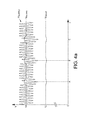
- Figure 4a shows the values of V supply , V filter and V drive for the circuit of Figure 4 .
- the value of the filtered voltage V filter is increased when the load is applied to the output of the voltage regulation device at points A, B and C. If the voltage at the gate terminal 44 of the MOSFET 36 increases in circumstances when the load is applied, the output voltage V drive of the voltage regulation device 26 has greater resilience to applied loads which is particularly advantageous during circumstances in which two injectors are operated simultaneously.
- the facility is provided to increase the value of V filter by providing a variable resistor element and/or a variable capacitor element in place of the respective elements 52 and 54, whilst omitting the current sensing device 59.
- the ECU 37 controls the value of the capacitor and/or resistor elements thus providing active control of the frequency response of the low pass filter 50.
- the output at the source terminal 42 can be increased during times of high power demand.
- FIG. 5 A further alternative embodiment is shown in Figure 5 . This embodiment is similar to those already described so only the differences are described in detail. Where appropriate like components are denoted with like reference numerals.
- the voltage regulation device 26 includes a differential amplifier 60 interposed between the low pass filter 50 and the MOSFET 36.
- the differential amplifier includes an inverting input 62, a non-inverting input 64 and an output 66 (hereinafter 'amplifier output').
- the node 56 of the low pass filter 50 is connected to the non-inverting input 64 of the differential amplifier 60 and the amplifier output 66 is connected to the gate terminal 44 of the MOSFET 36.
- the non-inverting input 64 receives the filtered voltage V filter of the power supply 22, which voltage therefore constitutes the set point of the differential amplifier 60.
- the inverting input 62 of the differential amplifier 60 is connected to the source terminal 42 of the MOSFET 36 such that the output of the MOSFET 36 is provided to the differential amplifier 60 as a feedback loop. Therefore, the differential amplifier 60 amplifies the difference between the inverting input 62 and the non-inverting input 64 and supplies the amplified difference to the gate terminal 44 of the MOSFET 36.
- the differential amplifier 60 increases the voltage input at the gate terminal 44 in response to an increased load applied by the injector driver stage 24. Therefore, the output terminal 32 of the MOSFET 36 is shielded from high frequency noise from the power supply 22 and exhibits improved robustness to high load conditions. The effect of this is to substantially eliminate the voltage droop at the output terminal 32 of the voltage regulation device 24 under a wide range of loads applied by the injector driver stage 24.
- the operating point of the MOSFET 36 is optimised by including a load element, in the form of a resistor element connected to ground, at the source terminal 42 of the MOSFET 36.
- the value of the resistor is selected as a function of the on-state resistance of the MOSFET 36.
Landscapes
- Engineering & Computer Science (AREA)
- Chemical & Material Sciences (AREA)
- Combustion & Propulsion (AREA)
- Mechanical Engineering (AREA)
- General Engineering & Computer Science (AREA)
- Fuel-Injection Apparatus (AREA)
- Continuous-Control Power Sources That Use Transistors (AREA)
Abstract
Description
- The present invention relates to an automotive fuel injection system and, more particularly, to an electrical drive arrangement for use in such a fuel injection system.
- Modern automotive vehicle engines are generally equipped with fuel injectors for injecting fuel (e.g. gasoline or diesel fuel) into the individual cylinders of the engine. The fuel injectors are coupled to a source of high pressure fuel that is delivered to the injectors by way of a fuel delivery system. The fuel injectors typically employ a valve needle that is actuated to disengage and re-engage an associated valve seat so as to control the amount of high pressure fuel that is metered from the fuel delivery system and injected into a corresponding engine cylinder. It is known to use solenoid operated injectors in which an electrically driven solenoid is operably connected to the valve needle. Energising the solenoid causes the valve needle to disengage from its seat, thus permitting fuel delivery, and de-energising the solenoid causes the valve needle to re-engage it seat, thus preventing fuel delivery.
- It is also known to use piezoelectrically operated fuel injectors that act either directly on the valve needle, or indirectly on the valve needle by way of a servo valve arrangement, to cause movement of the valve needle.
- The injectors of the engine are controlled by an electrical drive arrangement.
Figure 1 shows a simplified schematic of a knowndrive arrangement 2 which includes aninjector driver stage 4 that is supplied with power from avehicle power supply 6, typically the vehicle battery, and provides power and control inputs to one or more fuel injectors 8 (two of which are shown inFigure 1 ). - The
injector driver stage 4 is a circuit arrangement that is configured to select a specific one of theinjectors 8 for operation and to apply an operating voltage thereto. The functionality of theinjector driver stage 4 is controlled by an Engine Control Unit 10 (ECU) of the vehicle within which it is installed. - A known problem is that such electrical drive arrangements do not operate under ideal conditions and are typically supplied with electrical power that is subject to spurious electrical oscillations, hereinafter referred to as 'noise'. A significant proportion of power supply noise can be compensated for by the
injector drive stage 4 under the control of theECU 10 since some sources of noise are predictable. However, some sources of noise are not predictable and such noise affects detrimentally the level of control that theECU 10 has over the operational timing of theinjectors 8. - It is against this background that the invention provides an electrical drive arrangement of a fuel injection system comprising a power supply operatively connected to an injector driver stage which, in turn, is operatively connected to at least one fuel injector, and a voltage regulation device comprising an input terminal connected to the power supply and an output terminal connected to the injector driver stage and a field effect transistor including a drain terminal connected to the input terminal of the voltage regulation device, a source terminal connected to the output terminal of the voltage regulation device and a gate terminal. The filter device is operatively connected between the gate terminal of the field effect transistor and the input terminal of the voltage regulation device, thereby supplying a filtered voltage from the power supply as an input to the gate terminal. The filter device includes: i) a resistor element connected between the gate terminal and the input terminal; and ii) a capacitor element connected between the gate terminal and an electrical ground connection. A current sense element is connected between the capacitor element and the electrical ground connection, and a feedback path is connected therebetween to provide an injector voltage signal to the gate terminal of the voltage regulation device.
- This configuration provides the benefit that the voltage at the gate terminal of the field effect transistor is modified as a function of the load on the injector driver stage which adjusts the conductivity of the transistor thereby improving the load response of the voltage regulation device.
- The voltage regulation device is arranged to regulate the voltage input from the power supply.
- The invention provides an elegant solution to the problem of an electrical power supply that is inherently noisy which would otherwise affect detrimentally the performance of the fuel injectors.
- The voltage regulation device includes a field effect transistor connected between the power supply and the injector driver stage in a source follower configuration. More specifically, the voltage regulation device comprises an input terminal connected to the power supply and an output terminal connected to the injector driver stage wherein the field effect transistor is interposed between the input terminal and the output terminal.
- The field effect transistor may be a metal oxide semiconductor field effect transistor, preferably of the N-channel type.
- The aforementioned configuration ensures that the gate terminal of the field effect transistor is supplied with a relatively smooth voltage which has a corresponding effect on the conductivity of the field effect transistor from the source terminal to the drain terminal.
- In one embodiment, the filter device may take the form of a RC low pass filter circuit and may include a resistor element connected between the gate terminal and the input terminal of the voltage regulation device and a capacitor connected between the gate terminal and an electrical ground connection.
- Although such a circuit could be configured to have an operating point that is specific to the application in which the electrical drive arrangement is to be used, in one embodiment the resistor element and the capacitor element are selected so as to provide the filter device with a time constant of approximately 1 millisecond.
- In another embodiment, the value of the resistor element and/or the capacitor element are time-dependently variable thereby providing a means to modify the frequency response of the filter device. The frequency response of the voltage regulation device can therefore be tuned in order to optimise its operation for the type of devices e.g. fuel injectors with which it is used.
- A permanent electrical load, optionally in the form of a further resistor element, may be connected between the source terminal and the electrical ground connection in order to optimise the operating point of the field effect transistor. The ohmic value of the permanent electrical load may be selected as a function of the on-state resistance of the field effect transistor.
- In a further embodiment, the voltage regulation device includes a differential amplifier configured to amplify the voltage difference between the output voltage of the filter device and the voltage at the source terminal of the field effect transistor and supply an amplified output voltage to the gate terminal of the field effect transistor. The differential amplifier has the effect of increasing the voltage input at the gate terminal in response to an increased load applied by the injector drive stage.
- Reference has already been made to
Figure 1 which shows a known electrical drive arrangement for a fuel injection system. In order that the invention may be more readily understood, reference will now be made, by way of example only, to the accompanying drawings in which: -
Figure 2 is an electrical drive arrangement in accordance with an embodiment of the invention; -
Figure 3 is a detailed view of the electrical drive arrangement inFigure 2 ; -
Figure 3a is a graph showing voltage values of Vsupply, Vfilter, and Vdrive associated with the electrical drive arrangement shown inFigure 3 ; -
Figure 4 is detailed view of an electrical drive arrangement in accordance with an alternative embodiment of the invention; -
Figure 4a is a graph showing voltage values of Vsupply, Vfilter, and Vdrive associated with the electrical drive arrangement shown inFigure 4 ; and -
Figure 5 is a detailed view of an electrical drive arrangement in accordance with a further alternative embodiment of the invention. -
Figure 2 shows anelectrical drive arrangement 20 of a fuel injection system in which apower supply 22 is connected to aninjector driver stage 24 via avoltage regulation device 26. Thepower supply 22 is connected to aninput terminal 28 of thevoltage regulation device 26 via a firstvoltage supply line 30 and anoutput terminal 32 of thevoltage regulation device 26 is connected to theinjector driver stage 24 via a secondvoltage supply line 34. Although not shown inFigure 2 , thepower supply 22 is the battery of the vehicle in which theelectrical drive arrangement 20 is installed. Typically, thepower supply 22 supplies a nominal voltage of 12 or 24 Volts DC to thevoltage regulation device 26 and, thus, to theinjector driver stage 24. - Due to local electrical and electromagnetic influences, for example electrical components such as lighting and audio systems, emitters of electromagnetic interference such as vehicular-based telecommunication systems and the like, the DC voltage output from the
power supply 22 is not ideal but includes high frequency components superimposed thereon. Thevoltage regulation device 26 of the invention provides a means to stabilize the voltage that is input to theinjector driver stage 24 against the effects of the unstable DC supply voltage. - The
injector driver stage 24 is connected to a plurality of injectors 35 (only two of which are shown inFigure 2 for simplicity) and provides a means to select and electrically drive a specific injector under the control of an engine control unit 37 (ECU) in order to deliver a predetermined quantity of fuel. It should be appreciated that the configuration of theinjector driver stage 24 is not the focus of the invention and so will not be described in further detail here. - Referring to
Figure 3 , thevoltage regulation device 26 comprises an N-channel metal oxide semiconductor field-effect transistor 36 (hereinafter 'MOSFET') which includes adrain terminal 40, asource terminal 42 and agate terminal 44. Thedrain terminal 40 of theMOSFET 36 is connected to theinput terminal 28 of thevoltage regulation device 26 and thesource terminal 42 of theMOSFET 36 is connected to theoutput terminal 32 of thevoltage regulation device 26. - The
gate terminal 44 of theMOSFET 36 is connected to theinput terminal 28 of thevoltage regulation device 26 through alow pass filter 50 comprising aresistor element 52 and acapacitor element 54 that are connected to each other at anode 56. Thegate terminal 44 of theMOSFET 36 is connected to thenode 56 and is, therefore, connected to theinput terminal 28 through theresistor element 52 and is connected to aground connection 58 through thecapacitor element 54. Thelow pass filter 50 generates a filtered output voltage Vfilter at thenode 56 which forms an input voltage signal to thegate terminal 44 of theMOSFET 36. - The values of the
resistor element 52 and thecapacitor element 54 are configured to the electrical dynamics of the injector such that thelow pass filter 50 operates to block those frequencies present on thevoltage supply line 30 that theECU 37 cannot compensate and pass those frequencies which theECU 37 can compensate. - In the preferred embodiment of the invention, particularly advantageous values of the
resistor element 52 andcapacitor element 54 are selected so as to provide thelow pass filter 50 with a time constant of approximately 1 millisecond (ms), which corresponds to a filter cut-off frequency of approximately 160 Hertz (Hz). Furthermore, the value of thecapacitor element 54 is selected to be significantly greater than the parasitic capacitance of theMOSFET 36, preferably, between ten and one hundred times greater than the parasitic capacitance. - As is shown in
Figure 3 , theMOSFET 36 is arranged in a 'source follower', or 'common drain', configuration such that voltage between thegate terminal 44 and thesource terminal 42, which is derived from thelow pass filter 50, determines the conductivity of theMOSFET 36 from thedrain terminal 40 to thesource terminal 42. - Since the
gate terminal 44 is shielded from the high frequency noise present on thepower supply line 30 by thelow pass filter 50, the conductivity of theMOSFET 36 from thedrain terminal 40 to thesource terminal 42 is substantially constant compared to the 'raw' power supply voltage onsupply line 30. As a result, the voltage present at thesource terminal 42 of theMOSFET 36, and therefore the voltage present at theoutput terminal 32 of thevoltage regulation device 26, are substantially free from noise. - The beneficial effect of the
voltage regulation device 26 is clearly represented inFigure 3a . The voltage from the power supply 22 (Vsupply) is shown oscillating about a mean voltage level (substantially equal to Vfilter), which voltage is filtered by thelow pass filter 50 to provide the filtered voltage (Vfilter) at thegate terminal 44 of theMOSFET 36. The oscillating input voltage is shown to droop briefly at points A, B and C that are indicative of instances at which an electrical load is applied to the power supply, for example due to activation of an injector. However, the filtered supply voltage (Vfilter) is substantially unaffected by the voltage drops and thus supplies a substantially constant voltage source to thegate terminal 44. - The voltage Vdrive at the
output terminal 32 of thevoltage regulation device 26 substantially follows the filtered voltage Vfilter, although it is subject to a slight voltage droop at the instances that an electrical load is applied, at points A, B and C. Furthermore, it should be noted that the voltage present at the output terminal 32 (Vdrive) has a reduced value when compared to the mean voltage value of the voltage supply (Vsupply) by an amount substantially equal to the initiation voltage of theMOSFET 36. Since this reduction in voltage is a known value, and is predictable, theECU 37 is configured to compensate for the voltage reduction. - By virtue of the above circuit configuration, a smoother injector drive voltage is obtained which enables the
injector driver stage 24 to be substantially isolated from the noisy supply voltage. Moreover, the configuration of thevoltage regulation device 26 is elegantly simple thus providing a cost effective and reliable solution which does not significantly increase the overall complexity and cost of theelectrical drive arrangement 20. -
Figure 4 shows an another embodiment of the invention which reduces the sensitivity of the output voltage of thevoltage regulation device 26 to varying loads, particularly those that draw a high current from thepower supply 22, for example in circumstances in which it is necessary to operate more than one injector simultaneously. The embodiment ofFigure 4 is similar to the embodiment ofFigure 3 so only the differences are described in detail here and, where appropriate, like components are denoted by like reference numerals. - In
Figure 4 , thecapacitor element 54 of thelow pass filter 50 is not connected directly to theground connection 58 as it is in the embodiment ofFigure 3 . Instead, thecapacitor element 54 is connected to acurrent sensing element 59 which, in turn, is connected to theground connection 58. The high side of thecurrent sensing element 59 is also connected to afeedback path 57 from theinjector driver stage 24. - The
feedback path 57 provides a voltage value of a low voltage side of theinjectors 35 to the high side of thecurrent sensing element 59. Thecurrent sensing element 59 therefore senses the current that flows through theinjector driver stage 24 to theground connection 58. Since thefeedback path 57 is connected between thecapacitor element 54 and thecurrent sensing element 59, the voltage across thecapacitor element 54 is modified by the voltage across thecurrent sensing element 59 as a function of the current flowing through it. As a result, the voltage at thegate terminal 44 of theMOSFET 36 is modified as a function of the load on theinjector driver stage 24 such that the conductivity of theMOSFET 36 is adjusted accordingly. This improves the load response of thevoltage regulation device 26. -
Figure 4a shows the values of Vsupply, Vfilter and Vdrive for the circuit ofFigure 4 . When compared withFigure 3a , it can be seen that the value of the filtered voltage Vfilter is increased when the load is applied to the output of the voltage regulation device at points A, B and C. If the voltage at thegate terminal 44 of theMOSFET 36 increases in circumstances when the load is applied, the output voltage Vdrive of thevoltage regulation device 26 has greater resilience to applied loads which is particularly advantageous during circumstances in which two injectors are operated simultaneously. - Although the embodiment in
Figure 4 provides an elegant configuration that improves the resilience of thevoltage regulation device 26 to applied loads, in an alternative embodiment (not shown) the facility is provided to increase the value of Vfilter by providing a variable resistor element and/or a variable capacitor element in place of therespective elements current sensing device 59. In such an arrangement, theECU 37 controls the value of the capacitor and/or resistor elements thus providing active control of the frequency response of thelow pass filter 50. As a result, the output at thesource terminal 42 can be increased during times of high power demand. - A further alternative embodiment is shown in
Figure 5 . This embodiment is similar to those already described so only the differences are described in detail. Where appropriate like components are denoted with like reference numerals. - In
Figure 5 , thevoltage regulation device 26 includes adifferential amplifier 60 interposed between thelow pass filter 50 and theMOSFET 36. As is customary, the differential amplifier includes an invertinginput 62, anon-inverting input 64 and an output 66 (hereinafter 'amplifier output'). - The
node 56 of thelow pass filter 50 is connected to thenon-inverting input 64 of thedifferential amplifier 60 and theamplifier output 66 is connected to thegate terminal 44 of theMOSFET 36. Thus, thenon-inverting input 64 receives the filtered voltage Vfilter of thepower supply 22, which voltage therefore constitutes the set point of thedifferential amplifier 60. - The inverting
input 62 of thedifferential amplifier 60 is connected to thesource terminal 42 of theMOSFET 36 such that the output of theMOSFET 36 is provided to thedifferential amplifier 60 as a feedback loop. Therefore, thedifferential amplifier 60 amplifies the difference between the invertinginput 62 and thenon-inverting input 64 and supplies the amplified difference to thegate terminal 44 of theMOSFET 36. - As a result of the configuration of
Figure 5 , thedifferential amplifier 60 increases the voltage input at thegate terminal 44 in response to an increased load applied by theinjector driver stage 24. Therefore, theoutput terminal 32 of theMOSFET 36 is shielded from high frequency noise from thepower supply 22 and exhibits improved robustness to high load conditions. The effect of this is to substantially eliminate the voltage droop at theoutput terminal 32 of thevoltage regulation device 24 under a wide range of loads applied by theinjector driver stage 24. - It should be appreciated that various modifications may be made to the above described embodiments without departing from the scope of the inventive concept as defined by the appended claims.
- For example, in a further embodiment the operating point of the
MOSFET 36 is optimised by including a load element, in the form of a resistor element connected to ground, at thesource terminal 42 of theMOSFET 36. The value of the resistor is selected as a function of the on-state resistance of theMOSFET 36. - Alternative expressions of the inventive concept are set out in the following Clauses:
- 1. An electrical drive arrangement for at least one fuel injector of a fuel injection system comprising a power supply (22) operatively connected to an injector driver stage (24) which, in turn, is operatively connected to the at least one fuel injector (35), and a voltage regulation device (26) operatively connected between the power supply (22) and the injector driver stage (24), wherein the voltage regulation device (26) is arranged to regulate the voltage supplied from the power supply (22) to the injector driver stage (24).
- 2. The electrical drive arrangement of
Clause 1, wherein the voltage regulation device (26) includes a field effect transistor (36) connected between the power supply (22) and the injector driver stage (24) in a source follower configuration. - 3. The electrical drive arrangement of
Clause 2, wherein the voltage regulation device (26) further includes an input terminal (28) connected to the power supply (22) and an output terminal (32) connected to the injector driver stage (24) and wherein the field effect transistor (36) is interposed between the input terminal (28) and the output terminal (32). - 4. The electrical drive arrangement of Clause 3, wherein the field effect transistor (36) includes a drain terminal (40) connected to the input terminal (28) of the voltage regulation device (26), a source terminal (42) connected to the output terminal (32) of the voltage regulation device (26), and a gate terminal (44).
- 5. The electrical drive arrangement of
Clause 4, wherein a filter device (50) is operatively connected between the gate terminal (44) of the field effect transistor (36) and the input terminal (28) of the voltage regulation device (26), thereby supplying a filtered voltage (Vfilter) from the power supply (22) as an input to the gate terminal (44). - 6. The electrical drive arrangement of Clause 5, wherein the filter device (50) includes: i) a resistor element (52) connected between the gate terminal (44) and the input terminal (28); and ii) a capacitor element (54) connected between the gate terminal (44) and an electrical ground connection (58).
- 7. The electrical drive arrangement of
Clause 6, wherein the value of the resistor element (52) and/or the capacitor element (54) are variable thereby providing a means to modify the frequency response of the filter device (50). - 8. The electrical drive arrangement of
Clause 6 or Clause 7, including a load element connected between the source terminal (42) and the electrical ground connection (58), the ohmic value of the load element being selected as a function of the on-state resistance of the field effect transistor (36). - 9. The electrical drive arrangement of any one of
Clauses 6 to 8, wherein a current sense element (59) is connected between the capacitor element (54) and the electrical ground connection (58), and wherein a feedback path is connected therebetween to provide an injector voltage signal to the gate terminal (44) of the voltage regulation device (26). - 10. The electrical drive arrangement of any one of
Clauses 6 to 9, wherein the voltage regulation device (26) includes a differential amplifier (60) configured to amplify the voltage difference between the output voltage of the filter device (50) and the voltage at the source terminal (42) of the field effect transistor (36) and supply an amplified output voltage to the gate terminal (44) of the field effect transistor (36). - 11. The electrical drive arrangement of any one of
Clauses 2 to 10, wherein the field effect transistor (36) is a metal oxide semiconductor field effect transistor or an N-channel metal oxide semiconductor field effect transistor. - 12. An electrical drive arrangement for at least one fuel injector of a fuel injection system comprising:
- a power supply (22) connected to an injector driver stage (24) which, in turn, is connected to the at least one fuel injector (35),
- a voltage regulation device (26) connected between the power supply (22) and the injector driver stage (24) and having a gate terminal (44) and an input terminal (28),
- a filter device (50) connected between the gate terminal (44) of the voltage regulation device and the input terminal (28), thereby supplying a filtered voltage (Vfilter) from the power supply (22) as an input to the gate terminal (44), wherein the filter device (50) includes a resistor element (52) connected between the gate terminal (44) and the input terminal (28) and a capacitor element (54) connected between the gate terminal (44) and an electrical ground connection (58).
- 13. The electrical drive arrangement of
Clause 12, wherein the value of the resistor element (52) and/or the capacitor element (54) are variable thereby providing a means to modify the frequency response of the filter device (50). - 14. The electrical drive arrangement of
Clause 12 or Clause 13, wherein a current sense element (59) is connected between the capacitor element (54) and the electrical ground connection (58), and wherein a feedback path is connected therebetween to provide a injector voltage signal to the gate terminal (44). - 15. The electrical drive arrangement of any one of
Clauses 12 to 14, wherein the voltage regulation device (26) includes a differential amplifier (60) configured to amplify the voltage difference between the output voltage of the filter device (50) and the voltage at a source terminal (42) of the voltage regulation device (26) and supply an amplified output voltage to the gate terminal (44). - 16. An electrical drive arrangement for at least one fuel injector of a fuel injection system comprising:
- a power supply (22) connected to an injector driver stage (24) which, in turn, is connected to at least one fuel injector (35),
- a voltage regulation device (26) connected between the power supply (22) and the injector driver stage (24) and being arranged to regulate the voltage supplied from the power supply (22) to the injector driver stage (24), and
- a differential amplifier (60) which serves to increase the voltage input to the voltage regulation device (26) in response to an increased load applied to the injector driver stage (24).
- 17. The electrical drive arrangement of Clause 16, wherein the voltage regulation device (26) comprises an input terminal (28) connected to the power supply (22), an output terminal (32) connected to the injector driver stage (24) and a field effect transistor (36) disposed therebetween including a drain terminal (40) connected to the input terminal (28), a source terminal (42) connected to the output terminal (32), and a gate terminal (44).
- 18. The electrical drive arrangement of Clause 17, wherein a filter device (50) is connected between the gate terminal (44) of the field effect transistor (36) and the input terminal (28) of the voltage regulation device (26), thereby supplying a filtered voltage (Vfilter) from the power supply (22) as an input to the gate terminal (44).
- 19. The electrical drive arrangement of Clause 18, wherein the filter device (50) includes: i) a resistor element (52) connected between the gate terminal (44) and the input terminal (28); and ii) a capacitor element (54) connected between the gate terminal (44) and an electrical ground connection (58).
- 20. The electrical drive arrangement of Clause 19, wherein the value of the resistor element (52) and/or the capacitor element (54) are variable thereby providing a means to modify the frequency response of the filter device (50).
Claims (5)
- An electrical drive arrangement for at least one fuel injector of a fuel injection system comprising a power supply (22) operatively connected to an injector driver stage (24) which, in turn, is operatively connected to the at least one fuel injector (35), and a voltage regulation device (26) comprising an input terminal connected to the power supply (22) and an output terminal (32) connected to the injector driver stage (24) and a field effect transistor (36) including a drain terminal (40) connected to the input terminal (28) of the voltage regulation device (26), a source terminal (42) connected to the output terminal (32) of the voltage regulation device (26), and a gate terminal (44), wherein a filter device (50) is operatively connected between the gate terminal (44) of the field effect transistor (36) and the input terminal (28) of the voltage regulation device (26), thereby supplying a filtered voltage (Vfilter) from the power supply (22) as an input to the gate terminal (44), wherein the filter device (50) includes: i) a resistor element (52) connected between the gate terminal (44) and the input terminal (28); and ii) a capacitor element (54) connected between the gate terminal (44) and an electrical ground connection (58), wherein a current sense element (59) is connected between the capacitor element (54) and the electrical ground connection (58), and wherein a feedback path is connected therebetween to provide an injector voltage signal to the gate terminal (44) of the voltage regulation device (26).
- The electrical drive arrangement of claim 1, wherein the value of the resistor element (52) and/or the capacitor element (54) are variable thereby providing a means to modify the frequency response of the filter device (50).
- The electrical drive arrangement of claim 1 or claim 2, including a load element connected between the source terminal (42) and the electrical ground connection (58), the ohmic value of the load element being selected as a function of the on-state resistance of the field effect transistor (36).
- The electrical drive arrangement of any one of claims 1 to 3, wherein the voltage regulation device (26) includes a differential amplifier (60) configured to amplify the voltage difference between the output voltage of the filter device (50) and the voltage at the source terminal (42) of the field effect transistor (36) and supply an amplified output voltage to the gate terminal (44) of the field effect transistor (36).
- The electrical drive arrangement of any one of claims 1 to 4, wherein the field effect transistor (36) is a metal oxide semiconductor field effect transistor or an N-channel metal oxide semiconductor field effect transistor.
Applications Claiming Priority (2)
| Application Number | Priority Date | Filing Date | Title |
|---|---|---|---|
| US11/811,888 US7552718B2 (en) | 2007-06-12 | 2007-06-12 | Electrical drive arrangement for a fuel injection system |
| EP08760794A EP2167804B1 (en) | 2007-06-12 | 2008-06-10 | Electrical drive arrangement for a fuel injection system |
Related Parent Applications (2)
| Application Number | Title | Priority Date | Filing Date |
|---|---|---|---|
| EP08760794.1 Division | 2008-06-10 | ||
| EP08760794A Division EP2167804B1 (en) | 2007-06-12 | 2008-06-10 | Electrical drive arrangement for a fuel injection system |
Publications (2)
| Publication Number | Publication Date |
|---|---|
| EP2584183A1 true EP2584183A1 (en) | 2013-04-24 |
| EP2584183B1 EP2584183B1 (en) | 2014-08-13 |
Family
ID=39767216
Family Applications (2)
| Application Number | Title | Priority Date | Filing Date |
|---|---|---|---|
| EP12195288.1A Active EP2584183B1 (en) | 2007-06-12 | 2008-06-10 | Electrical Drive Arrangement for a Fuel Injection System |
| EP08760794A Active EP2167804B1 (en) | 2007-06-12 | 2008-06-10 | Electrical drive arrangement for a fuel injection system |
Family Applications After (1)
| Application Number | Title | Priority Date | Filing Date |
|---|---|---|---|
| EP08760794A Active EP2167804B1 (en) | 2007-06-12 | 2008-06-10 | Electrical drive arrangement for a fuel injection system |
Country Status (4)
| Country | Link |
|---|---|
| US (1) | US7552718B2 (en) |
| EP (2) | EP2584183B1 (en) |
| JP (1) | JP5069347B2 (en) |
| WO (1) | WO2008152039A1 (en) |
Families Citing this family (3)
| Publication number | Priority date | Publication date | Assignee | Title |
|---|---|---|---|---|
| EP2546499B1 (en) | 2011-07-14 | 2020-04-15 | Delphi Automotive Systems Luxembourg S.A. | Electrical drive arrangement for a fuel injection system |
| JP6987035B2 (en) * | 2018-09-27 | 2021-12-22 | 日立Astemo株式会社 | Electromagnetic valve drive device |
| KR102583207B1 (en) * | 2022-07-20 | 2023-09-25 | 주식회사 현대케피코 | Reset control system and method in vehicle |
Citations (6)
| Publication number | Priority date | Publication date | Assignee | Title |
|---|---|---|---|---|
| FR2547628A1 (en) * | 1983-06-18 | 1984-12-21 | Bosch Gmbh Robert | Computer controlled drive circuit for solenoid |
| US5381297A (en) * | 1993-06-18 | 1995-01-10 | Siemens Automotive L.P. | System and method for operating high speed solenoid actuated devices |
| GB2326956A (en) * | 1997-07-01 | 1999-01-06 | Bosch Gmbh Robert | Control means for controlling a load |
| JP2004072466A (en) * | 2002-08-07 | 2004-03-04 | Ntt Electornics Corp | Ripple filter circuit |
| DE10348265A1 (en) * | 2003-10-16 | 2005-05-19 | Robert Bosch Gmbh | Electronic circuit for driving inductive load, has boost converter with choke that functions as low-pass filter for noise pulses propagating towards input |
| WO2005119042A1 (en) * | 2004-06-04 | 2005-12-15 | Mikuni Corporation | Power supply apparatus |
Family Cites Families (7)
| Publication number | Priority date | Publication date | Assignee | Title |
|---|---|---|---|---|
| JPS5124743A (en) * | 1974-08-23 | 1976-02-28 | Matsushita Electric Industrial Co Ltd | Denatsuanteikakairo |
| JPS58170111A (en) * | 1982-03-30 | 1983-10-06 | Nippon Gakki Seizo Kk | Variable filter circuit |
| JPH0695809B2 (en) * | 1986-06-24 | 1994-11-24 | 日本電気株式会社 | Ripple filter circuit |
| US5681193A (en) * | 1995-07-25 | 1997-10-28 | Outboard Marine Corporation | Dual voltage regulated supply circuit for a marine propulsion device |
| JP3767764B2 (en) * | 1997-09-09 | 2006-04-19 | 三菱電機株式会社 | In-cylinder injection fuel control system for internal combustion engine |
| JP4045834B2 (en) * | 2002-04-01 | 2008-02-13 | 株式会社デンソー | Piezoelectric drive circuit |
| JP4745023B2 (en) * | 2005-11-07 | 2011-08-10 | フリースケール セミコンダクター インコーポレイテッド | Ripple filter circuit |
-
2007
- 2007-06-12 US US11/811,888 patent/US7552718B2/en active Active
-
2008
- 2008-06-10 WO PCT/EP2008/057235 patent/WO2008152039A1/en not_active Ceased
- 2008-06-10 EP EP12195288.1A patent/EP2584183B1/en active Active
- 2008-06-10 EP EP08760794A patent/EP2167804B1/en active Active
- 2008-06-10 JP JP2010507944A patent/JP5069347B2/en active Active
Patent Citations (6)
| Publication number | Priority date | Publication date | Assignee | Title |
|---|---|---|---|---|
| FR2547628A1 (en) * | 1983-06-18 | 1984-12-21 | Bosch Gmbh Robert | Computer controlled drive circuit for solenoid |
| US5381297A (en) * | 1993-06-18 | 1995-01-10 | Siemens Automotive L.P. | System and method for operating high speed solenoid actuated devices |
| GB2326956A (en) * | 1997-07-01 | 1999-01-06 | Bosch Gmbh Robert | Control means for controlling a load |
| JP2004072466A (en) * | 2002-08-07 | 2004-03-04 | Ntt Electornics Corp | Ripple filter circuit |
| DE10348265A1 (en) * | 2003-10-16 | 2005-05-19 | Robert Bosch Gmbh | Electronic circuit for driving inductive load, has boost converter with choke that functions as low-pass filter for noise pulses propagating towards input |
| WO2005119042A1 (en) * | 2004-06-04 | 2005-12-15 | Mikuni Corporation | Power supply apparatus |
Also Published As
| Publication number | Publication date |
|---|---|
| EP2584183B1 (en) | 2014-08-13 |
| EP2167804B1 (en) | 2013-01-16 |
| US7552718B2 (en) | 2009-06-30 |
| EP2167804A1 (en) | 2010-03-31 |
| WO2008152039A1 (en) | 2008-12-18 |
| US20080308070A1 (en) | 2008-12-18 |
| JP2010527084A (en) | 2010-08-05 |
| JP5069347B2 (en) | 2012-11-07 |
Similar Documents
| Publication | Publication Date | Title |
|---|---|---|
| US9653200B2 (en) | Electromagnetic-valve controller | |
| EP1903202B1 (en) | Apparatus for driving electromagnetic valves | |
| US8081498B2 (en) | Internal combustion engine controller | |
| JPS6056948B2 (en) | Solenoid valve drive device | |
| JPH0467204B2 (en) | ||
| JP2019143538A (en) | Load drive unit | |
| EP2167804B1 (en) | Electrical drive arrangement for a fuel injection system | |
| US5937828A (en) | Fuel injection injector controller | |
| US20100059023A1 (en) | Circuit Arrangement and Method for Operating an Inductive Load | |
| EP0756077B1 (en) | Electronic control circuit for an internal combustion engine | |
| US20190323447A1 (en) | Injection control device | |
| US11466650B2 (en) | Fuel injection valve driving device | |
| JP2018096229A (en) | Injection control device | |
| JP2007094970A (en) | Voltage supply circuit | |
| US8686697B2 (en) | DC voltage booster apparatus | |
| JP2011217245A (en) | Electromagnetic load control apparatus | |
| EP2546499B1 (en) | Electrical drive arrangement for a fuel injection system | |
| US11448174B2 (en) | Electromagnetic valve driving device | |
| JP2019190453A (en) | Injection control device | |
| JPH05272391A (en) | Fuel injection device | |
| EP0999354A2 (en) | Wide voltage range driver circuit for a fuel injector | |
| EP1669577A2 (en) | Inductive load driver with overcurrent detection | |
| US10957474B2 (en) | Injection control device | |
| US10961963B2 (en) | Injection control device | |
| US11391233B2 (en) | Method for controlling a high-pressure fuel injector |
Legal Events
| Date | Code | Title | Description |
|---|---|---|---|
| PUAI | Public reference made under article 153(3) epc to a published international application that has entered the european phase |
Free format text: ORIGINAL CODE: 0009012 |
|
| AC | Divisional application: reference to earlier application |
Ref document number: 2167804 Country of ref document: EP Kind code of ref document: P |
|
| AK | Designated contracting states |
Kind code of ref document: A1 Designated state(s): AT BE BG CH CY CZ DE DK EE ES FI FR GB GR HR HU IE IS IT LI LT LU LV MC MT NL NO PL PT RO SE SI SK TR |
|
| 17P | Request for examination filed |
Effective date: 20131024 |
|
| RBV | Designated contracting states (corrected) |
Designated state(s): AT BE BG CH CY CZ DE DK EE ES FI FR GB GR HR HU IE IS IT LI LT LU LV MC MT NL NO PL PT RO SE SI SK TR |
|
| GRAP | Despatch of communication of intention to grant a patent |
Free format text: ORIGINAL CODE: EPIDOSNIGR1 |
|
| INTG | Intention to grant announced |
Effective date: 20140211 |
|
| RAP1 | Party data changed (applicant data changed or rights of an application transferred) |
Owner name: DELPHI INTERNATIONAL OPERATIONS LUXEMBOURG S.A.R.L |
|
| GRAS | Grant fee paid |
Free format text: ORIGINAL CODE: EPIDOSNIGR3 |
|
| GRAA | (expected) grant |
Free format text: ORIGINAL CODE: 0009210 |
|
| AC | Divisional application: reference to earlier application |
Ref document number: 2167804 Country of ref document: EP Kind code of ref document: P |
|
| AK | Designated contracting states |
Kind code of ref document: B1 Designated state(s): AT BE BG CH CY CZ DE DK EE ES FI FR GB GR HR HU IE IS IT LI LT LU LV MC MT NL NO PL PT RO SE SI SK TR |
|
| REG | Reference to a national code |
Ref country code: GB Ref legal event code: FG4D |
|
| REG | Reference to a national code |
Ref country code: AT Ref legal event code: REF Ref document number: 682408 Country of ref document: AT Kind code of ref document: T Effective date: 20140815 Ref country code: CH Ref legal event code: EP |
|
| REG | Reference to a national code |
Ref country code: IE Ref legal event code: FG4D |
|
| REG | Reference to a national code |
Ref country code: DE Ref legal event code: R096 Ref document number: 602008033921 Country of ref document: DE Effective date: 20141002 |
|
| REG | Reference to a national code |
Ref country code: NL Ref legal event code: VDEP Effective date: 20140813 |
|
| REG | Reference to a national code |
Ref country code: AT Ref legal event code: MK05 Ref document number: 682408 Country of ref document: AT Kind code of ref document: T Effective date: 20140813 |
|
| REG | Reference to a national code |
Ref country code: LT Ref legal event code: MG4D |
|
| PG25 | Lapsed in a contracting state [announced via postgrant information from national office to epo] |
Ref country code: ES Free format text: LAPSE BECAUSE OF FAILURE TO SUBMIT A TRANSLATION OF THE DESCRIPTION OR TO PAY THE FEE WITHIN THE PRESCRIBED TIME-LIMIT Effective date: 20140813 Ref country code: GR Free format text: LAPSE BECAUSE OF FAILURE TO SUBMIT A TRANSLATION OF THE DESCRIPTION OR TO PAY THE FEE WITHIN THE PRESCRIBED TIME-LIMIT Effective date: 20141114 Ref country code: NO Free format text: LAPSE BECAUSE OF FAILURE TO SUBMIT A TRANSLATION OF THE DESCRIPTION OR TO PAY THE FEE WITHIN THE PRESCRIBED TIME-LIMIT Effective date: 20141113 Ref country code: BG Free format text: LAPSE BECAUSE OF FAILURE TO SUBMIT A TRANSLATION OF THE DESCRIPTION OR TO PAY THE FEE WITHIN THE PRESCRIBED TIME-LIMIT Effective date: 20141113 Ref country code: FI Free format text: LAPSE BECAUSE OF FAILURE TO SUBMIT A TRANSLATION OF THE DESCRIPTION OR TO PAY THE FEE WITHIN THE PRESCRIBED TIME-LIMIT Effective date: 20140813 Ref country code: PT Free format text: LAPSE BECAUSE OF FAILURE TO SUBMIT A TRANSLATION OF THE DESCRIPTION OR TO PAY THE FEE WITHIN THE PRESCRIBED TIME-LIMIT Effective date: 20141215 Ref country code: LT Free format text: LAPSE BECAUSE OF FAILURE TO SUBMIT A TRANSLATION OF THE DESCRIPTION OR TO PAY THE FEE WITHIN THE PRESCRIBED TIME-LIMIT Effective date: 20140813 Ref country code: SE Free format text: LAPSE BECAUSE OF FAILURE TO SUBMIT A TRANSLATION OF THE DESCRIPTION OR TO PAY THE FEE WITHIN THE PRESCRIBED TIME-LIMIT Effective date: 20140813 |
|
| PG25 | Lapsed in a contracting state [announced via postgrant information from national office to epo] |
Ref country code: AT Free format text: LAPSE BECAUSE OF FAILURE TO SUBMIT A TRANSLATION OF THE DESCRIPTION OR TO PAY THE FEE WITHIN THE PRESCRIBED TIME-LIMIT Effective date: 20140813 Ref country code: CY Free format text: LAPSE BECAUSE OF FAILURE TO SUBMIT A TRANSLATION OF THE DESCRIPTION OR TO PAY THE FEE WITHIN THE PRESCRIBED TIME-LIMIT Effective date: 20140813 Ref country code: LV Free format text: LAPSE BECAUSE OF FAILURE TO SUBMIT A TRANSLATION OF THE DESCRIPTION OR TO PAY THE FEE WITHIN THE PRESCRIBED TIME-LIMIT Effective date: 20140813 Ref country code: IS Free format text: LAPSE BECAUSE OF FAILURE TO SUBMIT A TRANSLATION OF THE DESCRIPTION OR TO PAY THE FEE WITHIN THE PRESCRIBED TIME-LIMIT Effective date: 20141213 Ref country code: HR Free format text: LAPSE BECAUSE OF FAILURE TO SUBMIT A TRANSLATION OF THE DESCRIPTION OR TO PAY THE FEE WITHIN THE PRESCRIBED TIME-LIMIT Effective date: 20140813 |
|
| PG25 | Lapsed in a contracting state [announced via postgrant information from national office to epo] |
Ref country code: NL Free format text: LAPSE BECAUSE OF FAILURE TO SUBMIT A TRANSLATION OF THE DESCRIPTION OR TO PAY THE FEE WITHIN THE PRESCRIBED TIME-LIMIT Effective date: 20140813 |
|
| PG25 | Lapsed in a contracting state [announced via postgrant information from national office to epo] |
Ref country code: RO Free format text: LAPSE BECAUSE OF FAILURE TO SUBMIT A TRANSLATION OF THE DESCRIPTION OR TO PAY THE FEE WITHIN THE PRESCRIBED TIME-LIMIT Effective date: 20140813 Ref country code: DK Free format text: LAPSE BECAUSE OF FAILURE TO SUBMIT A TRANSLATION OF THE DESCRIPTION OR TO PAY THE FEE WITHIN THE PRESCRIBED TIME-LIMIT Effective date: 20140813 Ref country code: CZ Free format text: LAPSE BECAUSE OF FAILURE TO SUBMIT A TRANSLATION OF THE DESCRIPTION OR TO PAY THE FEE WITHIN THE PRESCRIBED TIME-LIMIT Effective date: 20140813 Ref country code: SK Free format text: LAPSE BECAUSE OF FAILURE TO SUBMIT A TRANSLATION OF THE DESCRIPTION OR TO PAY THE FEE WITHIN THE PRESCRIBED TIME-LIMIT Effective date: 20140813 Ref country code: EE Free format text: LAPSE BECAUSE OF FAILURE TO SUBMIT A TRANSLATION OF THE DESCRIPTION OR TO PAY THE FEE WITHIN THE PRESCRIBED TIME-LIMIT Effective date: 20140813 |
|
| REG | Reference to a national code |
Ref country code: DE Ref legal event code: R097 Ref document number: 602008033921 Country of ref document: DE |
|
| PG25 | Lapsed in a contracting state [announced via postgrant information from national office to epo] |
Ref country code: PL Free format text: LAPSE BECAUSE OF FAILURE TO SUBMIT A TRANSLATION OF THE DESCRIPTION OR TO PAY THE FEE WITHIN THE PRESCRIBED TIME-LIMIT Effective date: 20140813 |
|
| PLBE | No opposition filed within time limit |
Free format text: ORIGINAL CODE: 0009261 |
|
| STAA | Information on the status of an ep patent application or granted ep patent |
Free format text: STATUS: NO OPPOSITION FILED WITHIN TIME LIMIT |
|
| 26N | No opposition filed |
Effective date: 20150515 |
|
| PG25 | Lapsed in a contracting state [announced via postgrant information from national office to epo] |
Ref country code: SI Free format text: LAPSE BECAUSE OF FAILURE TO SUBMIT A TRANSLATION OF THE DESCRIPTION OR TO PAY THE FEE WITHIN THE PRESCRIBED TIME-LIMIT Effective date: 20140813 |
|
| PG25 | Lapsed in a contracting state [announced via postgrant information from national office to epo] |
Ref country code: MC Free format text: LAPSE BECAUSE OF FAILURE TO SUBMIT A TRANSLATION OF THE DESCRIPTION OR TO PAY THE FEE WITHIN THE PRESCRIBED TIME-LIMIT Effective date: 20140813 Ref country code: IT Free format text: LAPSE BECAUSE OF NON-PAYMENT OF DUE FEES Effective date: 20150610 |
|
| REG | Reference to a national code |
Ref country code: CH Ref legal event code: PL |
|
| PG25 | Lapsed in a contracting state [announced via postgrant information from national office to epo] |
Ref country code: LU Free format text: LAPSE BECAUSE OF FAILURE TO SUBMIT A TRANSLATION OF THE DESCRIPTION OR TO PAY THE FEE WITHIN THE PRESCRIBED TIME-LIMIT Effective date: 20150610 |
|
| REG | Reference to a national code |
Ref country code: IE Ref legal event code: MM4A |
|
| PG25 | Lapsed in a contracting state [announced via postgrant information from national office to epo] |
Ref country code: CH Free format text: LAPSE BECAUSE OF NON-PAYMENT OF DUE FEES Effective date: 20150630 Ref country code: IE Free format text: LAPSE BECAUSE OF NON-PAYMENT OF DUE FEES Effective date: 20150610 Ref country code: LI Free format text: LAPSE BECAUSE OF NON-PAYMENT OF DUE FEES Effective date: 20150630 |
|
| REG | Reference to a national code |
Ref country code: FR Ref legal event code: PLFP Year of fee payment: 9 |
|
| PG25 | Lapsed in a contracting state [announced via postgrant information from national office to epo] |
Ref country code: BE Free format text: LAPSE BECAUSE OF FAILURE TO SUBMIT A TRANSLATION OF THE DESCRIPTION OR TO PAY THE FEE WITHIN THE PRESCRIBED TIME-LIMIT Effective date: 20140813 |
|
| PG25 | Lapsed in a contracting state [announced via postgrant information from national office to epo] |
Ref country code: MT Free format text: LAPSE BECAUSE OF FAILURE TO SUBMIT A TRANSLATION OF THE DESCRIPTION OR TO PAY THE FEE WITHIN THE PRESCRIBED TIME-LIMIT Effective date: 20140813 |
|
| PG25 | Lapsed in a contracting state [announced via postgrant information from national office to epo] |
Ref country code: HU Free format text: LAPSE BECAUSE OF FAILURE TO SUBMIT A TRANSLATION OF THE DESCRIPTION OR TO PAY THE FEE WITHIN THE PRESCRIBED TIME-LIMIT; INVALID AB INITIO Effective date: 20080610 |
|
| REG | Reference to a national code |
Ref country code: FR Ref legal event code: PLFP Year of fee payment: 10 |
|
| PG25 | Lapsed in a contracting state [announced via postgrant information from national office to epo] |
Ref country code: TR Free format text: LAPSE BECAUSE OF FAILURE TO SUBMIT A TRANSLATION OF THE DESCRIPTION OR TO PAY THE FEE WITHIN THE PRESCRIBED TIME-LIMIT Effective date: 20140813 |
|
| REG | Reference to a national code |
Ref country code: FR Ref legal event code: PLFP Year of fee payment: 11 |
|
| REG | Reference to a national code |
Ref country code: DE Ref legal event code: R081 Ref document number: 602008033921 Country of ref document: DE Owner name: DELPHI TECHNOLOGIES IP LIMITED, BB Free format text: FORMER OWNER: DELPHI INTERNATIONAL OPERATIONS LUXEMBOURG S.A R.L., BASCHARAGE, LU |
|
| REG | Reference to a national code |
Ref country code: GB Ref legal event code: 732E Free format text: REGISTERED BETWEEN 20190222 AND 20190227 |
|
| P01 | Opt-out of the competence of the unified patent court (upc) registered |
Effective date: 20230327 |
|
| REG | Reference to a national code |
Ref country code: DE Ref legal event code: R081 Ref document number: 602008033921 Country of ref document: DE Owner name: PHINIA DELPHI LUXEMBOURG SARL, LU Free format text: FORMER OWNER: DELPHI TECHNOLOGIES IP LIMITED, ST. MICHAEL, BB |
|
| PGFP | Annual fee paid to national office [announced via postgrant information from national office to epo] |
Ref country code: DE Payment date: 20250509 Year of fee payment: 18 |
|
| PGFP | Annual fee paid to national office [announced via postgrant information from national office to epo] |
Ref country code: GB Payment date: 20250508 Year of fee payment: 18 |
|
| PGFP | Annual fee paid to national office [announced via postgrant information from national office to epo] |
Ref country code: FR Payment date: 20250512 Year of fee payment: 18 |