EP2583936A1 - Optical air slit and method for manufacturing optical air slits - Google Patents
Optical air slit and method for manufacturing optical air slits Download PDFInfo
- Publication number
- EP2583936A1 EP2583936A1 EP12184771.9A EP12184771A EP2583936A1 EP 2583936 A1 EP2583936 A1 EP 2583936A1 EP 12184771 A EP12184771 A EP 12184771A EP 2583936 A1 EP2583936 A1 EP 2583936A1
- Authority
- EP
- European Patent Office
- Prior art keywords
- slit
- opening
- substrate
- layer
- portions
- Prior art date
- Legal status (The legal status is an assumption and is not a legal conclusion. Google has not performed a legal analysis and makes no representation as to the accuracy of the status listed.)
- Withdrawn
Links
Images


Classifications
-
- G—PHYSICS
- G03—PHOTOGRAPHY; CINEMATOGRAPHY; ANALOGOUS TECHNIQUES USING WAVES OTHER THAN OPTICAL WAVES; ELECTROGRAPHY; HOLOGRAPHY
- G03F—PHOTOMECHANICAL PRODUCTION OF TEXTURED OR PATTERNED SURFACES, e.g. FOR PRINTING, FOR PROCESSING OF SEMICONDUCTOR DEVICES; MATERIALS THEREFOR; ORIGINALS THEREFOR; APPARATUS SPECIALLY ADAPTED THEREFOR
- G03F7/00—Photomechanical, e.g. photolithographic, production of textured or patterned surfaces, e.g. printing surfaces; Materials therefor, e.g. comprising photoresists; Apparatus specially adapted therefor
- G03F7/0035—Multiple processes, e.g. applying a further resist layer on an already in a previously step, processed pattern or textured surface
-
- G—PHYSICS
- G02—OPTICS
- G02B—OPTICAL ELEMENTS, SYSTEMS OR APPARATUS
- G02B5/00—Optical elements other than lenses
- G02B5/005—Diaphragms
-
- G—PHYSICS
- G03—PHOTOGRAPHY; CINEMATOGRAPHY; ANALOGOUS TECHNIQUES USING WAVES OTHER THAN OPTICAL WAVES; ELECTROGRAPHY; HOLOGRAPHY
- G03F—PHOTOMECHANICAL PRODUCTION OF TEXTURED OR PATTERNED SURFACES, e.g. FOR PRINTING, FOR PROCESSING OF SEMICONDUCTOR DEVICES; MATERIALS THEREFOR; ORIGINALS THEREFOR; APPARATUS SPECIALLY ADAPTED THEREFOR
- G03F7/00—Photomechanical, e.g. photolithographic, production of textured or patterned surfaces, e.g. printing surfaces; Materials therefor, e.g. comprising photoresists; Apparatus specially adapted therefor
- G03F7/20—Exposure; Apparatus therefor
-
- G—PHYSICS
- G03—PHOTOGRAPHY; CINEMATOGRAPHY; ANALOGOUS TECHNIQUES USING WAVES OTHER THAN OPTICAL WAVES; ELECTROGRAPHY; HOLOGRAPHY
- G03F—PHOTOMECHANICAL PRODUCTION OF TEXTURED OR PATTERNED SURFACES, e.g. FOR PRINTING, FOR PROCESSING OF SEMICONDUCTOR DEVICES; MATERIALS THEREFOR; ORIGINALS THEREFOR; APPARATUS SPECIALLY ADAPTED THEREFOR
- G03F7/00—Photomechanical, e.g. photolithographic, production of textured or patterned surfaces, e.g. printing surfaces; Materials therefor, e.g. comprising photoresists; Apparatus specially adapted therefor
- G03F7/26—Processing photosensitive materials; Apparatus therefor
- G03F7/40—Treatment after imagewise removal, e.g. baking
-
- G—PHYSICS
- G01—MEASURING; TESTING
- G01J—MEASUREMENT OF INTENSITY, VELOCITY, SPECTRAL CONTENT, POLARISATION, PHASE OR PULSE CHARACTERISTICS OF INFRARED, VISIBLE OR ULTRAVIOLET LIGHT; COLORIMETRY; RADIATION PYROMETRY
- G01J3/00—Spectrometry; Spectrophotometry; Monochromators; Measuring colours
- G01J3/02—Details
- G01J3/0205—Optical elements not provided otherwise, e.g. optical manifolds, diffusers, windows
- G01J3/0229—Optical elements not provided otherwise, e.g. optical manifolds, diffusers, windows using masks, aperture plates, spatial light modulators or spatial filters, e.g. reflective filters
-
- Y—GENERAL TAGGING OF NEW TECHNOLOGICAL DEVELOPMENTS; GENERAL TAGGING OF CROSS-SECTIONAL TECHNOLOGIES SPANNING OVER SEVERAL SECTIONS OF THE IPC; TECHNICAL SUBJECTS COVERED BY FORMER USPC CROSS-REFERENCE ART COLLECTIONS [XRACs] AND DIGESTS
- Y10—TECHNICAL SUBJECTS COVERED BY FORMER USPC
- Y10T—TECHNICAL SUBJECTS COVERED BY FORMER US CLASSIFICATION
- Y10T428/00—Stock material or miscellaneous articles
- Y10T428/24—Structurally defined web or sheet [e.g., overall dimension, etc.]
- Y10T428/24273—Structurally defined web or sheet [e.g., overall dimension, etc.] including aperture
- Y10T428/24298—Noncircular aperture [e.g., slit, diamond, rectangular, etc.]
- Y10T428/24314—Slit or elongated
Definitions
- This disclosure relates generally to optical slits and more particularly to method for making relatively long, narrow optical air slits.
- air slits have a wide range of use in optics.
- One such use is in hyper spectral imaging system where such systems are used to collect and process information from across the electromagnetic spectrum that can extend beyond the visible band.
- techniques used to form air optical slits include the use of laser cutting, photolithography, Electro Discharge Machining (EDM), thin film deposition, e-beam lithography, RF /DC & reactive sputtering, Chemical Vapor Deposition (CVD), Physical Vapor Deposition (PVD).Chemical wet etch, electroplating, electro etching, sputter etching and ion milling.
- EDM Electro Discharge Machining
- thin film deposition e-beam lithography
- RF /DC & reactive sputtering RF /DC & reactive sputtering
- CVD Chemical Vapor Deposition
- PVD Physical Vapor Deposition
- a structure having an optical slit therein, comprising: a substrate having an opening there through; and a metal layer disposed on the substrate, such metal layer having a slit therein, such slit being narrower than the opening and being disposed over the opening, portions of the metal layer disposed adjacent the slit being suspended over the opening and other portions of the metal layer being supported by the substrate.
- a method for forming a structure having an optical slit therein. The method includes: forming an opening through a portion of a substrate; filling the opening with a sacrificial material, such material extending through a portion of the opening with portion of the material being disposed onto adjacent portions of an upper surface of the substrate; polishing the sacrificial material to remove the portions of the sacrificial material disposed onto adjacent portions of the upper surface of the substrate; forming a metalized layer on the upper surface of the substrate and the polished sacrificial material; applying a photolithographically processable material on an upper surface of the metalized layer; photolihographically forming a slit in the photolithographically processable material to expose a portion of the upper surface of the metallized layer , such slit being disposed over the opening in the portion of the substrate; etching to remove the exposed portion of the upper surface of the metalized layer to expose the sacrificial material while retaining unexposed portions of the method
- the unexposed portions of the metallized layer are electroplated to a predetermined thickness.
- the electroplating is performed prior to the forming of the slit.
- the electroplating is performed subsequent to forming of the slit.
- the opening is formed using laser cutting.
- a substrate 10 is provided.
- the substrate 10 is, for example, Aluminum Oxide, Silicon Nitride, Beryllium oxide or any rigid material with low coefficient of thermal expansion, here for example in the range of 0.55 x 10 -6 /°C to 8.4 x 10 -6 /°C.
- the substrate 10 has a thickness in the range of 3 to 10 mils.
- an opening 12 ( FIG. 2 ) is formed through a portion of the substrate 10.
- the opening 12 is formed using laser cutting.
- the opening 12 has a span in the order 1 to 2 mils.
- the opening 12 is filled with a sacrificial material 14, such material having portions 14a extending through the opening 12 with portion 14b of the material 12 being disposed onto adjacent portions of an upper surface 16 of the substrate 10, as shown in FIG. 3 .
- the sacrificial matter 14 is adhesively bonded to the substrate 10 and is here, for example, Crystalbond 590, Manufactured by Electron Microscopy Sciences, P.O. Box 550, 1560 Industry Road, Hatfield, PA. 19440, Sycast manufactured by Emerson & Cuming, Henkel Corporation, Canton ( Electronic Materials) 869 Washington Street, Canton, MA 02021,United States Or AZ-photo resist AZ Electronics Materials (USA) corp., 70 Meister Ave. Somerville, NJ 08876-1252.
- the upper surface of the structure is polished to remove the portions 14a, 14b of the sacrificial material 14 disposed onto adjacent portions of the upper surface 16 of the substrate 10 as shown in FIG. 4 .
- a metalized layer 18 is deposited, for example electroplated, on the upper surface of the substrate 12 and the polished sacrificial material 14, as shown in FIG. 5 .
- the metalized layer 18 is formed by E-Beam, Sputtering, Electrolysis and laminating methods.
- the metallization layer 18 is here for example, a refractory metal such as titanium-tungsten or chromium.
- the metallization layer 18 may be initially formed as a relatively thin seed layer, for example, having a thickness in the range of 150 to 250 Angstroms, or be formed with a thickness by electroplating in the range of 0.5 to 2 mils.
- a conventional photolithographically processable material 20 is deposited on an upper surface of the metalized layer 18, as shown in FIG. 6 .
- a slit 24 is photolihographically formed in the photolithographically processable material 20 using any conventional photolithographic-etching technique to expose an underlying portion of the upper surface of the metallized layer 18, such slit being disposed over the filled opening 12 in FIG 1 in the portion of the substrate 10, as shown in FIG. 7 .
- the slit 24 has a width in the range of 5 um to 60 um and a length in the range of 77 mm to 112 mm.
- the exposed underlying portion of the metalized layer 18 is removed by any conventional etching process to form there a slit 26 having a width in the range of 5 um to 60 um and a length in the range of 77 mm to 112 mm., as shown in FIG. 7 . It is noted that the slits 24, 26 expose the sacrificial material 14 while retaining unexposed portions of the metallized layer 18.
- the photoresist layer 20 is removed.
- the metalized layer 18, here acts as a seed layer and is electroplated with material 28;
- material 25 is, for example, gold, copper, nickel, chromium or any standard electroplate-able metal used in the electroplating business, to form the resulting metalized layer 18 with a resulting predetermined thickness, here in the range of .5 mil to 1 mil; it being noted that the electroplating leaves a slit 26 in the material 28 so that slits 24, 26 are formed in the resulting metalized layer 18.
- the metalized layer 18 may be formed by electroplating the unexposed portions of the metallized layer to a predetermined thickness either prior to forming the slit 26 or subsequent to forming the slit 26.
- the structure shown in FIG, 8 is a structure having an optical slit 24, 26 therein, comprising: substrate 10 having the opening 12 therethrough; and a metal layer 16, 18 disposed on the substrate 10, such metal layer 16. 18 having a slit 24, 26 therein, such slit 24, 26 being narrower than the opening 12 and being disposed over the opening 12, portions of the metal layer 16a, 18a disposed adjacent the slit 24, 26 being suspended over the opening 12 and other portions of the metal layer 16, 18 being supported by the substrate 10.
Landscapes
- Physics & Mathematics (AREA)
- General Physics & Mathematics (AREA)
- Optics & Photonics (AREA)
- Micromachines (AREA)
- Measurement Of Radiation (AREA)
Abstract
Description
- This disclosure relates generally to optical slits and more particularly to method for making relatively long, narrow optical air slits.
- As is known in the art, air slits have a wide range of use in optics. One such use is in hyper spectral imaging system where such systems are used to collect and process information from across the electromagnetic spectrum that can extend beyond the visible band.
- As is also known, techniques used to form air optical slits include the use of laser cutting, photolithography, Electro Discharge Machining (EDM), thin film deposition, e-beam lithography, RF /DC & reactive sputtering, Chemical Vapor Deposition (CVD), Physical Vapor Deposition (PVD).Chemical wet etch, electroplating, electro etching, sputter etching and ion milling.
- In accordance with the disclosure, a structure is provided having an optical slit therein, comprising: a substrate having an opening there through; and a metal layer disposed on the substrate, such metal layer having a slit therein, such slit being narrower than the opening and being disposed over the opening, portions of the metal layer disposed adjacent the slit being suspended over the opening and other portions of the metal layer being supported by the substrate.
- In one embodiment, a method is provided for forming a structure having an optical slit therein. The method includes: forming an opening through a portion of a substrate; filling the opening with a sacrificial material, such material extending through a portion of the opening with portion of the material being disposed onto adjacent portions of an upper surface of the substrate; polishing the sacrificial material to remove the portions of the sacrificial material disposed onto adjacent portions of the upper surface of the substrate; forming a metalized layer on the upper surface of the substrate and the polished sacrificial material; applying a photolithographically processable material on an upper surface of the metalized layer; photolihographically forming a slit in the photolithographically processable material to expose a portion of the upper surface of the metallized layer , such slit being disposed over the opening in the portion of the substrate; etching to remove the exposed portion of the upper surface of the metalized layer to expose the sacrificial material while retaining unexposed portions of the metallized layer; and removing the sacrificial layer and the photolithographically processable material.
- In one embodiment, the unexposed portions of the metallized layer are electroplated to a predetermined thickness.
- In one embodiment, the electroplating is performed prior to the forming of the slit.
- In one embodiment, the electroplating is performed subsequent to forming of the slit.
- In one embodiment, the opening is formed using laser cutting.
- The details of one or more embodiments of the disclosure are set forth in the accompanying drawings and the description below. Other features, objects, and advantages of the disclosure will be apparent from the description and drawings, and from the claims.
-
-
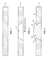
FIGS. 1-8 show a sequence of steps used to form a structure having an optical slit therein according to the disclosure. - Like reference symbols in the various drawings indicate like elements.
- Referring now to
FIGS. 1-8 , steps used to form a structure having an optical slit therein are illustrated. Thus, referring toFIG. 1 , asubstrate 10 is provided. Here thesubstrate 10 is, for example, Aluminum Oxide, Silicon Nitride, Beryllium oxide or any rigid material with low coefficient of thermal expansion, here for example in the range of 0.55 x 10⁻⁶/°C to 8.4 x 10⁻⁶/°C. Here, thesubstrate 10 has a thickness in the range of 3 to 10 mils. - Next, an opening 12 (
FIG. 2 ) is formed through a portion of thesubstrate 10. Here, for example, theopening 12 is formed using laser cutting. The opening 12 has a span in the order 1 to 2 mils. - Next, the
opening 12 is filled with asacrificial material 14, such material having portions 14a extending through theopening 12 withportion 14b of thematerial 12 being disposed onto adjacent portions of anupper surface 16 of thesubstrate 10, as shown inFIG. 3 . Here, thesacrificial matter 14 is adhesively bonded to thesubstrate 10 and is here, for example, Crystalbond 590, Manufactured by Electron Microscopy Sciences, P.O. Box 550, 1560 Industry Road, Hatfield, PA. 19440, Sycast manufactured by Emerson & Cuming, Henkel Corporation, Canton ( Electronic Materials) 869 Washington Street, Canton, MA 02021,United States Or AZ-photo resist AZ Electronics Materials (USA) corp., 70 Meister Ave. Somerville, NJ 08876-1252. Next, the upper surface of the structure is polished to remove theportions 14a, 14b of thesacrificial material 14 disposed onto adjacent portions of theupper surface 16 of thesubstrate 10 as shown inFIG. 4 . - Next, a
metalized layer 18 is deposited, for example electroplated, on the upper surface of thesubstrate 12 and the polishedsacrificial material 14, as shown inFIG. 5 . Here, for example, themetalized layer 18 is formed by E-Beam, Sputtering, Electrolysis and laminating methods. Themetallization layer 18 is here for example, a refractory metal such as titanium-tungsten or chromium. Here themetallization layer 18 may be initially formed as a relatively thin seed layer, for example, having a thickness in the range of 150 to 250 Angstroms, or be formed with a thickness by electroplating in the range of 0.5 to 2 mils. - Next, a conventional photolithographically
processable material 20 is deposited on an upper surface of themetalized layer 18, as shown inFIG. 6 . - Next, a
slit 24 is photolihographically formed in the photolithographicallyprocessable material 20 using any conventional photolithographic-etching technique to expose an underlying portion of the upper surface of themetallized layer 18, such slit being disposed over the filledopening 12 inFIG 1 in the portion of thesubstrate 10, as shown inFIG. 7 . Here, theslit 24 has a width in the range of 5 um to 60 um and a length in the range of 77 mm to 112 mm. - Next, the exposed underlying portion of the
metalized layer 18 is removed by any conventional etching process to form there aslit 26 having a width in the range of 5 um to 60 um and a length in the range of 77 mm to 112 mm., as shown inFIG. 7 . It is noted that theslits sacrificial material 14 while retaining unexposed portions of the metallizedlayer 18. - Next, the
photoresist layer 20 is removed. - Next, the
metalized layer 18, here acts as a seed layer and is electroplated withmaterial 28; here material 25 is, for example, gold, copper, nickel, chromium or any standard electroplate-able metal used in the electroplating business, to form the resultingmetalized layer 18 with a resulting predetermined thickness, here in the range of .5 mil to 1 mil; it being noted that the electroplating leaves aslit 26 in thematerial 28 so thatslits metalized layer 18. It should be noted that themetalized layer 18 may be formed by electroplating the unexposed portions of the metallized layer to a predetermined thickness either prior to forming theslit 26 or subsequent to forming theslit 26. - Next, the
sacrificial layer 14 is removed using for example, chemical solvents, epoxy stripper, oxygen plasma, and oxygen ion milling to form the structure shown inFIG. 8 . Thus, the structure shown inFIG, 8 is a structure having anoptical slit substrate 10 having the opening 12 therethrough; and ametal layer substrate 10,such metal layer 16. 18 having aslit such slit opening 12, portions of themetal layer slit opening 12 and other portions of themetal layer substrate 10. - A number of embodiments of the disclosure have been described. Nevertheless, it will be understood that various modifications may be made without departing from the spirit and scope of the disclosure. Accordingly, other embodiments are within the scope of the following claims.
Claims (6)
- A method for forming a structure having an optical slit therein, comprising;
forming an opening through a portion of a substrate;
filling the opening with a sacrificial material, such material extending through a portion of the opening with portion of the material being disposed onto adjacent portions of an upper surface of the substrate;
polishing the sacrificial material to remove the portions of the sacrificial material disposed onto adjacent portions of the upper surface of the substrate;
forming a metalized layer on the upper surface of the substrate and the polished sacrificial material;
applying a photolithographically processable material on an upper surface of the metalized layer;
photolihographically forming a slit in the photolithographically processable material to expose a portion of the upper surface of the metallized layer, such slit being disposed over the opening in the portion of the substrate;
etching to remove the exposed portion of the upper surface of the metaled .layer to expose the sacrificial material while retaining unexposed portions of the metallized layer;
removing the sacrificial layer and the photolithographically processable material. - The method recited in claim 1 including electroplating the unexposed portions of the metallized layer to a predetermined thickness.
- The method recited in claim 2 wherein the electroplating is performed prior to the forming of the slit.
- The method recited in claim 2 wherein the electroplating is performed subsequent to forming of the slit.
- The method recited in claim 1 wherein the opening is formed using laser cutting.
- A structure having an optical slit therein, comprising:a substrate having an opening therethrough;a metal layer disposed on the substrate, such metal layer having a slit therein, such slit being narrower than the opening and being disposed over the opening, portions of the metal layer disposed adjacent the slit being suspended over the opening and other portions of the metal layer being supported by the substrate.
Applications Claiming Priority (1)
| Application Number | Priority Date | Filing Date | Title |
|---|---|---|---|
| US13/278,254 US20130101788A1 (en) | 2011-10-21 | 2011-10-21 | Optical air slit and method for manufacturing optical air slits |
Publications (1)
| Publication Number | Publication Date |
|---|---|
| EP2583936A1 true EP2583936A1 (en) | 2013-04-24 |
Family
ID=47221926
Family Applications (1)
| Application Number | Title | Priority Date | Filing Date |
|---|---|---|---|
| EP12184771.9A Withdrawn EP2583936A1 (en) | 2011-10-21 | 2012-09-18 | Optical air slit and method for manufacturing optical air slits |
Country Status (3)
| Country | Link |
|---|---|
| US (2) | US20130101788A1 (en) |
| EP (1) | EP2583936A1 (en) |
| IL (1) | IL221840A (en) |
Citations (3)
| Publication number | Priority date | Publication date | Assignee | Title |
|---|---|---|---|---|
| US5781331A (en) * | 1997-01-24 | 1998-07-14 | Roxburgh Ltd. | Optical microshutter array |
| US6248509B1 (en) * | 1999-07-27 | 2001-06-19 | James E. Sanford | Maskless photoresist exposure system using mems devices |
| US20060009038A1 (en) * | 2004-07-12 | 2006-01-12 | International Business Machines Corporation | Processing for overcoming extreme topography |
Family Cites Families (7)
| Publication number | Priority date | Publication date | Assignee | Title |
|---|---|---|---|---|
| US3374705A (en) | 1965-10-23 | 1968-03-26 | Fabri Tek Inc | Optical slit apparatus |
| US5384662A (en) | 1993-07-12 | 1995-01-24 | The Regents Of The University Of California | Precision optical slit for high heat load or ultra high vacuum |
| US6238581B1 (en) * | 1998-12-18 | 2001-05-29 | Eastman Kodak Company | Process for manufacturing an electro-mechanical grating device |
| JP2000326300A (en) * | 1999-03-17 | 2000-11-28 | Seiko Instruments Inc | Near-field optical head, method of manufacturing the same, and optical recording / reproducing apparatus using the same |
| JP2001208987A (en) | 2001-02-20 | 2001-08-03 | Advantest Corp | Variable width optical slit mechanism |
| US6552788B1 (en) | 2001-07-09 | 2003-04-22 | Ruda & Associates | Hyperspectral imaging using linear chromatic aberration |
| JP2004037317A (en) | 2002-07-04 | 2004-02-05 | Murata Mfg Co Ltd | Three-dimensional shape measuring method and three-dimensional shape measuring device |
-
2011
- 2011-10-21 US US13/278,254 patent/US20130101788A1/en not_active Abandoned
-
2012
- 2012-09-09 IL IL221840A patent/IL221840A/en active IP Right Grant
- 2012-09-18 EP EP12184771.9A patent/EP2583936A1/en not_active Withdrawn
-
2014
- 2014-07-28 US US14/444,294 patent/US9235115B2/en active Active
Patent Citations (3)
| Publication number | Priority date | Publication date | Assignee | Title |
|---|---|---|---|---|
| US5781331A (en) * | 1997-01-24 | 1998-07-14 | Roxburgh Ltd. | Optical microshutter array |
| US6248509B1 (en) * | 1999-07-27 | 2001-06-19 | James E. Sanford | Maskless photoresist exposure system using mems devices |
| US20060009038A1 (en) * | 2004-07-12 | 2006-01-12 | International Business Machines Corporation | Processing for overcoming extreme topography |
Also Published As
| Publication number | Publication date |
|---|---|
| IL221840A (en) | 2017-10-31 |
| US20130101788A1 (en) | 2013-04-25 |
| US9235115B2 (en) | 2016-01-12 |
| US20140335458A1 (en) | 2014-11-13 |
Similar Documents
| Publication | Publication Date | Title |
|---|---|---|
| US10910185B2 (en) | Method for the fabrication of electron field emission devices including carbon nanotube electron field emission devices | |
| US6465158B1 (en) | Semiconductor wafer dividing method | |
| US9613780B2 (en) | Method of fabricating sample support membrane | |
| US20100140497A1 (en) | Membrane supports with reinforcement features | |
| US9060419B2 (en) | Substrate formed on carrier having retaining features and resultant electronic device | |
| US6289583B1 (en) | Method for making cards with multiple contact tips for testing semiconductor chips | |
| CN110636417B (en) | Microphone and method for manufacturing microphone | |
| CN1834282B (en) | Film forming apparatus, film forming method | |
| EP2590203B1 (en) | Method of fabricating a beam-defining aperture for a focused ion beam and beam definition of a focused ion beam with such an aperture | |
| Bagolini et al. | Silicon deep reactive ion etching with aluminum hard mask | |
| CN109819390B (en) | Manufacturing method of GMR/TMR microphone | |
| EP2750160A2 (en) | Phase plate and method of fabricating same | |
| CN107275472A (en) | High-temperature superconducting thin film nanometer bridge knot preparation method | |
| KR101923841B1 (en) | Metal hard mask and method for producing same | |
| Hou et al. | Characterization of Sputtered Nano-Au Layer Deposition on Silicon Wafer | |
| US9235115B2 (en) | Optical air slit and method for manufacturing optical air slits | |
| US20200371628A1 (en) | Touch structure, manufacturing method thereof, and touch display device | |
| US20020112963A1 (en) | Methods for fabricating high-precision thermally stable electromagnetic coils | |
| US20060228823A1 (en) | MEMS structure with anodically bonded silicon-on-insulator substrate | |
| US20250243578A1 (en) | Mask and Preparation Method Thereof | |
| US8252363B2 (en) | Method of thinning a block transferred to a substrate | |
| JP5608462B2 (en) | Manufacturing method of imprint mold | |
| EP2100176B1 (en) | Substrates with slotted metals and related methods | |
| US7160751B2 (en) | Method of making a SOI silicon structure | |
| JP3945561B2 (en) | Method for producing extraction electrode |
Legal Events
| Date | Code | Title | Description |
|---|---|---|---|
| PUAI | Public reference made under article 153(3) epc to a published international application that has entered the european phase |
Free format text: ORIGINAL CODE: 0009012 |
|
| AK | Designated contracting states |
Kind code of ref document: A1 Designated state(s): AL AT BE BG CH CY CZ DE DK EE ES FI FR GB GR HR HU IE IS IT LI LT LU LV MC MK MT NL NO PL PT RO RS SE SI SK SM TR |
|
| AX | Request for extension of the european patent |
Extension state: BA ME |
|
| RIN1 | Information on inventor provided before grant (corrected) |
Inventor name: CAIGOY, ARTURO L. |
|
| 17P | Request for examination filed |
Effective date: 20131024 |
|
| RBV | Designated contracting states (corrected) |
Designated state(s): AL AT BE BG CH CY CZ DE DK EE ES FI FR GB GR HR HU IE IS IT LI LT LU LV MC MK MT NL NO PL PT RO RS SE SI SK SM TR |
|
| 17Q | First examination report despatched |
Effective date: 20150611 |
|
| GRAP | Despatch of communication of intention to grant a patent |
Free format text: ORIGINAL CODE: EPIDOSNIGR1 |
|
| STAA | Information on the status of an ep patent application or granted ep patent |
Free format text: STATUS: GRANT OF PATENT IS INTENDED |
|
| INTG | Intention to grant announced |
Effective date: 20200217 |
|
| STAA | Information on the status of an ep patent application or granted ep patent |
Free format text: STATUS: THE APPLICATION IS DEEMED TO BE WITHDRAWN |
|
| 18D | Application deemed to be withdrawn |
Effective date: 20200630 |