EP2582033A2 - Control for a multi-level active rectifier - Google Patents
Control for a multi-level active rectifier Download PDFInfo
- Publication number
- EP2582033A2 EP2582033A2 EP12187670.0A EP12187670A EP2582033A2 EP 2582033 A2 EP2582033 A2 EP 2582033A2 EP 12187670 A EP12187670 A EP 12187670A EP 2582033 A2 EP2582033 A2 EP 2582033A2
- Authority
- EP
- European Patent Office
- Prior art keywords
- phase
- active rectifier
- monitored
- input voltage
- frequency
- Prior art date
- Legal status (The legal status is an assumption and is not a legal conclusion. Google has not performed a legal analysis and makes no representation as to the accuracy of the status listed.)
- Withdrawn
Links
- 238000005070 sampling Methods 0.000 claims abstract description 18
- 230000004044 response Effects 0.000 claims abstract description 10
- 238000004364 calculation method Methods 0.000 claims description 9
- 230000001360 synchronised effect Effects 0.000 claims description 7
- 238000000034 method Methods 0.000 claims 6
- 238000012544 monitoring process Methods 0.000 abstract description 3
- 230000006870 function Effects 0.000 description 7
- 238000010586 diagram Methods 0.000 description 4
- 239000003990 capacitor Substances 0.000 description 2
- 230000007423 decrease Effects 0.000 description 2
- 230000008859 change Effects 0.000 description 1
- 238000006243 chemical reaction Methods 0.000 description 1
- 230000001939 inductive effect Effects 0.000 description 1
- 239000000463 material Substances 0.000 description 1
- 238000005259 measurement Methods 0.000 description 1
- 238000012986 modification Methods 0.000 description 1
- 230000004048 modification Effects 0.000 description 1
- 238000007493 shaping process Methods 0.000 description 1
- 230000005428 wave function Effects 0.000 description 1
Images

Classifications
-
- H—ELECTRICITY
- H02—GENERATION; CONVERSION OR DISTRIBUTION OF ELECTRIC POWER
- H02M—APPARATUS FOR CONVERSION BETWEEN AC AND AC, BETWEEN AC AND DC, OR BETWEEN DC AND DC, AND FOR USE WITH MAINS OR SIMILAR POWER SUPPLY SYSTEMS; CONVERSION OF DC OR AC INPUT POWER INTO SURGE OUTPUT POWER; CONTROL OR REGULATION THEREOF
- H02M7/00—Conversion of AC power input into DC power output; Conversion of DC power input into AC power output
- H02M7/66—Conversion of AC power input into DC power output; Conversion of DC power input into AC power output with possibility of reversal
- H02M7/68—Conversion of AC power input into DC power output; Conversion of DC power input into AC power output with possibility of reversal by static converters
- H02M7/72—Conversion of AC power input into DC power output; Conversion of DC power input into AC power output with possibility of reversal by static converters using discharge tubes with control electrode or semiconductor devices with control electrode
- H02M7/79—Conversion of AC power input into DC power output; Conversion of DC power input into AC power output with possibility of reversal by static converters using discharge tubes with control electrode or semiconductor devices with control electrode using devices of a triode or transistor type requiring continuous application of a control signal
- H02M7/797—Conversion of AC power input into DC power output; Conversion of DC power input into AC power output with possibility of reversal by static converters using discharge tubes with control electrode or semiconductor devices with control electrode using devices of a triode or transistor type requiring continuous application of a control signal using semiconductor devices only
-
- H—ELECTRICITY
- H02—GENERATION; CONVERSION OR DISTRIBUTION OF ELECTRIC POWER
- H02M—APPARATUS FOR CONVERSION BETWEEN AC AND AC, BETWEEN AC AND DC, OR BETWEEN DC AND DC, AND FOR USE WITH MAINS OR SIMILAR POWER SUPPLY SYSTEMS; CONVERSION OF DC OR AC INPUT POWER INTO SURGE OUTPUT POWER; CONTROL OR REGULATION THEREOF
- H02M7/00—Conversion of AC power input into DC power output; Conversion of DC power input into AC power output
- H02M7/02—Conversion of AC power input into DC power output without possibility of reversal
- H02M7/04—Conversion of AC power input into DC power output without possibility of reversal by static converters
- H02M7/12—Conversion of AC power input into DC power output without possibility of reversal by static converters using discharge tubes with control electrode or semiconductor devices with control electrode
- H02M7/21—Conversion of AC power input into DC power output without possibility of reversal by static converters using discharge tubes with control electrode or semiconductor devices with control electrode using devices of a triode or transistor type requiring continuous application of a control signal
- H02M7/217—Conversion of AC power input into DC power output without possibility of reversal by static converters using discharge tubes with control electrode or semiconductor devices with control electrode using devices of a triode or transistor type requiring continuous application of a control signal using semiconductor devices only
-
- H—ELECTRICITY
- H02—GENERATION; CONVERSION OR DISTRIBUTION OF ELECTRIC POWER
- H02M—APPARATUS FOR CONVERSION BETWEEN AC AND AC, BETWEEN AC AND DC, OR BETWEEN DC AND DC, AND FOR USE WITH MAINS OR SIMILAR POWER SUPPLY SYSTEMS; CONVERSION OF DC OR AC INPUT POWER INTO SURGE OUTPUT POWER; CONTROL OR REGULATION THEREOF
- H02M1/00—Details of apparatus for conversion
- H02M1/0003—Details of control, feedback or regulation circuits
-
- H—ELECTRICITY
- H02—GENERATION; CONVERSION OR DISTRIBUTION OF ELECTRIC POWER
- H02M—APPARATUS FOR CONVERSION BETWEEN AC AND AC, BETWEEN AC AND DC, OR BETWEEN DC AND DC, AND FOR USE WITH MAINS OR SIMILAR POWER SUPPLY SYSTEMS; CONVERSION OF DC OR AC INPUT POWER INTO SURGE OUTPUT POWER; CONTROL OR REGULATION THEREOF
- H02M7/00—Conversion of AC power input into DC power output; Conversion of DC power input into AC power output
- H02M7/42—Conversion of DC power input into AC power output without possibility of reversal
- H02M7/44—Conversion of DC power input into AC power output without possibility of reversal by static converters
- H02M7/48—Conversion of DC power input into AC power output without possibility of reversal by static converters using discharge tubes with control electrode or semiconductor devices with control electrode
- H02M7/483—Converters with outputs that each can have more than two voltages levels
- H02M7/487—Neutral point clamped inverters
Definitions
- the present invention is related to active rectifiers, and in particular to control architectures for active rectifiers.
- active rectifiers In contrast with passive rectifiers that rely on diodes to rectify an alternating current (AC) input to a direct current (DC) output, active rectifiers employ solid-state switching devices that are selectively turned On and Off to convert an AC input to a DC output. Operation of the active rectifier is controlled by a controller that generates control signals provided to each of the plurality of solid-state switching devices within the active rectifier. Benefits of the active rectifier include the ability to regulate the output voltage of the active rectifier, reduce current harmonics and provide improved power factor correction.
- the performance of the active rectifier relies, in part, on the ability of the controller to accurately determine the phase and frequency of the AC input voltage.
- power factor correction relies on shaping the AC input current drawn by the active rectifier to be in-phase with the AC input voltage. It is therefore important to be able to accurately measure the phase (i.e., position) of the AC input voltage.
- the present invention is a control architecture for a three-level active rectifier.
- the control architecture monitors the AC input voltage provided to the active rectifier at a sampling rate grater than the frequency of the AC input voltage and calculates, in response, a phase estimate associated with the monitored AC input voltage that is updated with each new sample of the AC input voltage. Based on the phase and frequency estimates, along with monitoring of the AC input current and DC output voltage, the control architecture calculates voltage commands that are used to generate the pulse-width modulation (PWM) controls signals for provision to solid-state switching devices in the active rectifier.
- PWM pulse-width modulation
- FIG. 1 is a block diagram of an active rectifier system according to an embodiment of the present invention.
- FIG. 2 is a block diagram illustrating functions performed by a phase/frequency detector according to an embodiment of the present invention.
- the control architecture of the present invention controls the operation of a multi-level rectifier by sampling the AC input at a sampling frequency significantly higher than the frequency of the AC input voltage. This higher sampling rate minimizes the error in the calculated phase and frequency.
- Calculation of pulse width modulation (PWM) control signals generated by the control architecture can be synchronized with calculated phase information such that each calculation of PWM control signals is based on a most recent update of calculated phase information. With improved phase information, the control architecture is able to reduce harmonics, which provide improved power factor correction that in turn improves power quality and reduces the electromagnetic interference (EMI) associated with the active rectifier.
- PWM pulse width modulation
- FIG. 1 is a block diagram of active rectifier system 10 according to an embodiment of the present invention.
- active rectifier system 10 includes active rectifier 12 and a control architecture that includes two co-processors, control processor 14, and PWM/angle processor 16.
- control processor 14 and PWM/angle processor 16 may be performed by a single processor.
- active rectifier 12 is a multi-level active rectifier that converts a three-phase alternating current (AC) input labeled Vas, Vbs, Vcs to a multi-level DC output that includes a positive DC voltage (Vdc+), a negative DC voltage (Vdc-), and a midpoint voltage (Vm).
- Active rectifier 12 includes inductive filters La, Lb, Lc, DC link capacitors C1, C2, and a plurality of solid-state switching devices illustrated here for the sake of simplicity as single-pole, multiple-throw switches S1, S2, S3 that selectively connect each phase of AC input to one of the plurality of DC outputs.
- each switch S1, S2, S3 would be comprised of a plurality of solid-state switches configured to provide an AC input to one of the plurality of DC outputs (e.g., Vdc+, Vdc-, Vm).
- PWM/angle processor 16 includes phase/frequency detector 18 and pulse width modulator (PWM) 20.
- Phase/frequency detector 18 monitors the AC input voltage Vas, Vbs, Vcs supplied to active rectifier 12 and calculates based on the monitored AC input phase and frequency information (labeled "0" and " ⁇ ", respectively).
- Phase/frequency processor 16 samples the AC input voltage Vas, Vbs, Vcs at a frequency much greater than the frequency of the AC input voltage (e.g., ten times greater), and in one embodiment at a frequency greater than the operating frequency of switches S1-S3. In one embodiment, the sampling rate is selected based on the particular power quality requirements of an application. In the embodiment shown in FIG.
- PWM/angle processor 16 which may be implemented as a stand-alone processor, a field-programmable gate array (FPGA), or digital signal processor (DSP).
- PWM/angle processor 16 employs a phase lock loop (PLL) to generate phase information ⁇ and frequency information ⁇ .
- PLL phase lock loop
- PWM 20 employs phase information 0 to convert voltage commands (e.g., Vq, Yd ) provided by current regulator 22 from a two-phase dq reference frame to a three-phase abc reference frame (e.g., Vs1, Vs2, Vs3, representing PWM duty cycle command signals provided to switches S1, S2, and S3).
- calculation of duty cycle information by PWM 20 is synchronized with updated phase information provided by phase/frequency detector 18, such that each PWM calculation is made with a most recent estimate of phase information ⁇ from phase/frequency detector 18.
- PWM 20 and phase/frequency detector 18 By placing PWM 20 and phase/frequency detector 18 in the same processor, PWM 20 is able to retrieve without significant delay the most recent phase information ⁇ calculated by phase/frequency detector 18. This does not mean that the update rate of phase/frequency detector 18 and update rate of PWM 20 must be the same.
- the update rate of each may be selected independent of the update rate of the other to meet the desired EMI performance and power quality performance for a particular application.
- Control processor 14 includes current regulator 22 and voltage regulator 24.
- Voltage regulator 24 monitors the DC output voltages Vc1, Vc2 provided across capacitors C1 and C2, respectively.
- voltage regulator 24 receives the monitored DC output voltages Vc1, Vc2, and compares the monitored voltages to a desired or reference DC output voltage. The difference or error between the monitored DC output voltages and the desired DC output voltage is provided as an input to current regulator 22, which selectively increases or decreases the current command provided to PWM 20 based on the received error.
- Current regulator 22 monitors the AC currents ia, ib, ic provided to active rectifier 12, and receives phase information ⁇ and frequency information ⁇ provided by phase/frequency detector 18.
- Current regulator 22 provides power factor correction by monitoring current ia, ib, ic supplied to active rectifier 12, and generating control signals provided to PWM 20 to control the DC output voltage (based on the input provided by voltage regulator 24) and to ensure that the monitored currents ia, ib, ic are in-phase with the monitored voltage as indicated by the phase and frequency information provided by phase/frequency detector 18.
- phase information ⁇ is employed by current regulator 22 to transform the monitored currents from the three-phase abc reference frame to a two-phase dq reference frame.
- Frequency information ⁇ is employed by current regulator 22 to decouple the dq phase currents as part of the dq proportional-integral (P-I) control loops provided within current regulator 22.
- current regulator 22 calculates duty cycle voltage commands (provided with respect to the two-phase dq reference frame, Vq, Yd ) for provision to PWM 20.
- Improved accuracy of phase information ⁇ provided by phase/frequency detector 18 improves the power factor correction provided by current regulator 22, thereby reducing the EMI associated with active rectifier 12.
- pulse width modulator (PWM) 20 receives duty cycle command instructions ( Yq, Yd ) from current regulator 22, and in response generates PWM signals that are supplied to each of the plurality of solid-state switching devices S1, S2, S3 included within active rectifier 12.
- the conversion of duty cycle command instructions Vq, Yd from the two-phase dq reference frame to the three-phase abc reference frame Ys1, Vs2, Vs3 is based, in part, on the accuracy of the phase information ⁇ provided by phase/frequency detector 18.
- the magnitude of current harmonics e.g., 2 nd , 3 rd , 4 th , etc.
- Minimizing the current harmonics results in improved power quality, which in turn, improves EMI performance of active rectifier 12.
- the update rate or frequency of PWM 20 does not need to be the same as the update rate or frequency of phase/frequency detector 18.
- PWM 20 may be synchronized with phase/frequency detector 18 to ensure that each duty cycle command instruction calculated by PWM 20 is based on a most recent estimate of position.
- the sample rate or update rate of phase/frequency detector may be some multiple of the update rate of PWM 20, such that phase/frequency detector 18 is synchronized with PWM 20, yet the update or sample rate of each may be selected independent of one another.
- the sampling frequency employed by phase/frequency detector 18 and the PWM frequency employed by PWM 20 can be selected independent of one another to meet the desired EMI and power quality requirements of a particular application.
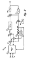
- FIG. 2 is a block diagram of functions performed by phase/frequency detector 18 according to an embodiment of the present invention to detect the position (i.e., phase ⁇ ) of the monitored AC input voltages Vas, Vbs, Vcs.
- the functions illustrated in FIG. 2 implement a phase-lock loop system, in which the phase ⁇ provided by phase/frequency processor 16 is updated with each sample of the monitored input.
- the monitored AC input voltage (represented here as monitored voltage sense signals Vas, Vbs, Vcs) are converted from a three-phase reference frame (abc) to a two-phase reference frame ( ⁇ ) by abc- ⁇ transform 30.
- Multiplier block 32 multiplies the signal ⁇ by the sine of the phase-lock loop angle PLL_angle, which represents the most recent phase estimate.
- multiplier block 34 multiplies the signal ⁇ by the cosine of the phase-lock look angle PLL_angle.
- the outputs of multiplier blocks 32 and 34 are compared by difference block 36 to calculate a difference or error between the signals that represents the difference between the current phase estimate and the phase indicated by the monitored AC input voltages Vas, Vbs, Vcs.
- Equation 1 is based on the assumption that the sampling rate is great enough that phase advancement between the current phase estimate and the phase of the monitored AC input voltage is relatively small (i.e., x ⁇ y).
- the calculated error between the monitored AC input and the current phase estimate is provided to proportional-integral (PI) controller 38 to generate an output that acts to drive the difference between the monitored error to zero.
- PI controller 36 is combined with the current position estimate ⁇ at summer block 40 to generate a new position estimate ⁇ .
- Wrapping block 42 provides wrapping (if necessary) of the new position estimate if it extends beyond a desired range (i.e., wraps the estimate back around within a desired range, e.g., 0-360 degrees), and provides the new position estimate ⁇ to control processor 14.
- the new position estimate ⁇ is also provided in feedback to correct subsequent estimates of the monitored position.
- the position estimate ⁇ is held in memory by block 44 so that this value may be used in the next software cycle by summer block 40.
- summer block 46 adds an offset 48 of -90 degrees to align the phase of the software algorithm with the hardware sensors.
- the resultant phase-lock loop signal (PLL_angle) is provided to sine function 50 and cosine function 52 to generate sine and cosine wave functions based on the new position estimate.
- the embodiment shown in FIG. 2 represents one such implementation of a phase-lock loop circuit used to estimate position of a signal and update estimates a signal based on subsequent measurements.
- the sample rate i.e., the rate at which AC voltages are sampled
- the frequency of the AC input voltage e.g., 100 times greater than the AC input frequency.
- the phase estimate ⁇ provided to control processor 14 is continuously updated. This is in contrast with typical zero cross systems in which the phase is updated only at zero cross of the monitored AC input. For example, if the AC input voltage is provided at 800 Hz, the position estimate ⁇ is updated at a frequency of 1600 Hz (representing two zero-cross events during each cycle). In the present invention, the phase estimate ⁇ may be updated at a sampling rate much greater than that of the AC input voltage (e.g., 100 KHz).
- sampling rate of the present invention may be selected based on the particular harmonics to be reduced. Therefore, the sampling rate may change based on the frequency of the AC input voltage or the particular harmonics to be minimized.
Landscapes
- Engineering & Computer Science (AREA)
- Power Engineering (AREA)
- Rectifiers (AREA)
Abstract
Description
- The present invention is related to active rectifiers, and in particular to control architectures for active rectifiers.
- In contrast with passive rectifiers that rely on diodes to rectify an alternating current (AC) input to a direct current (DC) output, active rectifiers employ solid-state switching devices that are selectively turned On and Off to convert an AC input to a DC output. Operation of the active rectifier is controlled by a controller that generates control signals provided to each of the plurality of solid-state switching devices within the active rectifier. Benefits of the active rectifier include the ability to regulate the output voltage of the active rectifier, reduce current harmonics and provide improved power factor correction.
- The performance of the active rectifier relies, in part, on the ability of the controller to accurately determine the phase and frequency of the AC input voltage. For example, power factor correction relies on shaping the AC input current drawn by the active rectifier to be in-phase with the AC input voltage. It is therefore important to be able to accurately measure the phase (i.e., position) of the AC input voltage.
- The present invention is a control architecture for a three-level active rectifier. The control architecture monitors the AC input voltage provided to the active rectifier at a sampling rate grater than the frequency of the AC input voltage and calculates, in response, a phase estimate associated with the monitored AC input voltage that is updated with each new sample of the AC input voltage. Based on the phase and frequency estimates, along with monitoring of the AC input current and DC output voltage, the control architecture calculates voltage commands that are used to generate the pulse-width modulation (PWM) controls signals for provision to solid-state switching devices in the active rectifier.
-
FIG. 1 is a block diagram of an active rectifier system according to an embodiment of the present invention. -
FIG. 2 is a block diagram illustrating functions performed by a phase/frequency detector according to an embodiment of the present invention. - The control architecture of the present invention controls the operation of a multi-level rectifier by sampling the AC input at a sampling frequency significantly higher than the frequency of the AC input voltage. This higher sampling rate minimizes the error in the calculated phase and frequency. Calculation of pulse width modulation (PWM) control signals generated by the control architecture can be synchronized with calculated phase information such that each calculation of PWM control signals is based on a most recent update of calculated phase information. With improved phase information, the control architecture is able to reduce harmonics, which provide improved power factor correction that in turn improves power quality and reduces the electromagnetic interference (EMI) associated with the active rectifier.
-
FIG. 1 is a block diagram ofactive rectifier system 10 according to an embodiment of the present invention. In the embodiment shown inFIG. 1 ,active rectifier system 10 includes active rectifier 12 and a control architecture that includes two co-processors, control processor 14, and PWM/angle processor 16. In other embodiments, the functions performed by control processor 14 and PWM/angle processor 16 may be performed by a single processor. - In the embodiment shown in
FIG. 1 , active rectifier 12 is a multi-level active rectifier that converts a three-phase alternating current (AC) input labeled Vas, Vbs, Vcs to a multi-level DC output that includes a positive DC voltage (Vdc+), a negative DC voltage (Vdc-), and a midpoint voltage (Vm). Active rectifier 12 includes inductive filters La, Lb, Lc, DC link capacitors C1, C2, and a plurality of solid-state switching devices illustrated here for the sake of simplicity as single-pole, multiple-throw switches S1, S2, S3 that selectively connect each phase of AC input to one of the plurality of DC outputs. In actuality, each switch S1, S2, S3 would be comprised of a plurality of solid-state switches configured to provide an AC input to one of the plurality of DC outputs (e.g., Vdc+, Vdc-, Vm). - In the embodiment shown in
FIG. 1 , PWM/angle processor 16 includes phase/frequency detector 18 and pulse width modulator (PWM) 20. Phase/frequency detector 18 monitors the AC input voltage Vas, Vbs, Vcs supplied to active rectifier 12 and calculates based on the monitored AC input phase and frequency information (labeled "0" and "ω", respectively). Phase/frequency processor 16 samples the AC input voltage Vas, Vbs, Vcs at a frequency much greater than the frequency of the AC input voltage (e.g., ten times greater), and in one embodiment at a frequency greater than the operating frequency of switches S1-S3. In one embodiment, the sampling rate is selected based on the particular power quality requirements of an application. In the embodiment shown inFIG. 1 , the increased sampling of the AC input voltage is provided by dedicated PWM/angle processor 16, which may be implemented as a stand-alone processor, a field-programmable gate array (FPGA), or digital signal processor (DSP). As described in more detail with respect toFIG. 2 , PWM/angle processor 16 employs a phase lock loop (PLL) to generate phase information θ and frequency information ω. - In the embodiment shown in
FIG. 1 , PWM 20 employs phase information 0 to convert voltage commands (e.g., Vq, Yd) provided by current regulator 22 from a two-phase dq reference frame to a three-phase abc reference frame (e.g., Vs1, Vs2, Vs3, representing PWM duty cycle command signals provided to switches S1, S2, and S3). In one embodiment, calculation of duty cycle information by PWM 20 is synchronized with updated phase information provided by phase/frequency detector 18, such that each PWM calculation is made with a most recent estimate of phase information θ from phase/frequency detector 18. By placing PWM 20 and phase/frequency detector 18 in the same processor, PWM 20 is able to retrieve without significant delay the most recent phase information θ calculated by phase/frequency detector 18. This does not mean that the update rate of phase/frequency detector 18 and update rate of PWM 20 must be the same. The update rate of each may be selected independent of the update rate of the other to meet the desired EMI performance and power quality performance for a particular application. - In the embodiment shown in
FIG. 1 , a second co-processor is employed in conjunction with PWM/angle processor 16. Control processor 14 includes current regulator 22 andvoltage regulator 24.Voltage regulator 24 monitors the DC output voltages Vc1, Vc2 provided across capacitors C1 and C2, respectively. In the embodiment shown inFIG. 1 ,voltage regulator 24 receives the monitored DC output voltages Vc1, Vc2, and compares the monitored voltages to a desired or reference DC output voltage. The difference or error between the monitored DC output voltages and the desired DC output voltage is provided as an input to current regulator 22, which selectively increases or decreases the current command provided to PWM 20 based on the received error. - Current regulator 22 monitors the AC currents ia, ib, ic provided to active rectifier 12, and receives phase information θ and frequency information ω provided by phase/
frequency detector 18. Current regulator 22 provides power factor correction by monitoring current ia, ib, ic supplied to active rectifier 12, and generating control signals provided to PWM 20 to control the DC output voltage (based on the input provided by voltage regulator 24) and to ensure that the monitored currents ia, ib, ic are in-phase with the monitored voltage as indicated by the phase and frequency information provided by phase/frequency detector 18. In particular, phase information θ is employed by current regulator 22 to transform the monitored currents from the three-phase abc reference frame to a two-phase dq reference frame. Frequency information ω is employed by current regulator 22 to decouple the dq phase currents as part of the dq proportional-integral (P-I) control loops provided within current regulator 22. In response to these inputs, current regulator 22 calculates duty cycle voltage commands (provided with respect to the two-phase dq reference frame, Vq, Yd) for provision to PWM 20. Improved accuracy of phase information θ provided by phase/frequency detector 18 improves the power factor correction provided by current regulator 22, thereby reducing the EMI associated with active rectifier 12. - As discussed above, pulse width modulator (PWM) 20 receives duty cycle command instructions (Yq, Yd) from current regulator 22, and in response generates PWM signals that are supplied to each of the plurality of solid-state switching devices S1, S2, S3 included within active rectifier 12. The conversion of duty cycle command instructions Vq, Yd from the two-phase dq reference frame to the three-phase abc reference frame Ys1, Vs2, Vs3 is based, in part, on the accuracy of the phase information θ provided by phase/
frequency detector 18. By improving the accuracy of phase information θ, the magnitude of current harmonics (e.g., 2nd, 3rd, 4th, etc.) is reduced. Minimizing the current harmonics results in improved power quality, which in turn, improves EMI performance of active rectifier 12. - As discussed above, the update rate or frequency of PWM 20 does not need to be the same as the update rate or frequency of phase/
frequency detector 18. However, PWM 20 may be synchronized with phase/frequency detector 18 to ensure that each duty cycle command instruction calculated by PWM 20 is based on a most recent estimate of position. For example, the sample rate or update rate of phase/frequency detector may be some multiple of the update rate of PWM 20, such that phase/frequency detector 18 is synchronized with PWM 20, yet the update or sample rate of each may be selected independent of one another. In this way, the sampling frequency employed by phase/frequency detector 18 and the PWM frequency employed by PWM 20 can be selected independent of one another to meet the desired EMI and power quality requirements of a particular application. -
FIG. 2 is a block diagram of functions performed by phase/frequency detector 18 according to an embodiment of the present invention to detect the position (i.e., phase θ) of the monitored AC input voltages Vas, Vbs, Vcs. The functions illustrated inFIG. 2 implement a phase-lock loop system, in which the phase θ provided by phase/frequency processor 16 is updated with each sample of the monitored input. - In the embodiment shown in
FIG. 2 , the monitored AC input voltage (represented here as monitored voltage sense signals Vas, Vbs, Vcs) are converted from a three-phase reference frame (abc) to a two-phase reference frame (αβ) by abc-αβ transform 30. Multiplier block 32 multiplies the signal α by the sine of the phase-lock loop angle PLL_angle, which represents the most recent phase estimate. Likewise, multiplier block 34 multiplies the signal β by the cosine of the phase-lock look angle PLL_angle. The outputs of multiplier blocks 32 and 34 are compared by difference block 36 to calculate a difference or error between the signals that represents the difference between the current phase estimate and the phase indicated by the monitored AC input voltages Vas, Vbs, Vcs. The functions performed in calculating the error between the current phase estimate and the phase of the monitored AC input voltage in the embodiment shown inFIG. 2 can be represented mathematically by the following equation:
where x = phase of the monitored AC voltage; and
y = current phase estimate. - As discussed above, the phase of the monitored AC input voltage when converted from the abc reference frame to the αβ reference frame is related to the phase of the AC input voltage (e.g., α = Va, β = 0.57735*(Vb-Vc)).
Equation 1 is based on the assumption that the sampling rate is great enough that phase advancement between the current phase estimate and the phase of the monitored AC input voltage is relatively small (i.e., x ≈ y). - The calculated error between the monitored AC input and the current phase estimate is provided to proportional-integral (PI)
controller 38 to generate an output that acts to drive the difference between the monitored error to zero. The output of PI controller 36 is combined with the current position estimate θ at summer block 40 to generate a new position estimate θ. Wrapping block 42 provides wrapping (if necessary) of the new position estimate if it extends beyond a desired range (i.e., wraps the estimate back around within a desired range, e.g., 0-360 degrees), and provides the new position estimate θ to control processor 14. - The new position estimate θ is also provided in feedback to correct subsequent estimates of the monitored position. The position estimate θ is held in memory by block 44 so that this value may be used in the next software cycle by summer block 40. In addition, summer block 46 adds an offset 48 of -90 degrees to align the phase of the software algorithm with the hardware sensors. The resultant phase-lock loop signal (PLL_angle) is provided to
sine function 50 andcosine function 52 to generate sine and cosine wave functions based on the new position estimate. The embodiment shown inFIG. 2 represents one such implementation of a phase-lock loop circuit used to estimate position of a signal and update estimates a signal based on subsequent measurements. - In one embodiment, the sample rate (i.e., the rate at which AC voltages are sampled) is much greater than the frequency of the AC input voltage (e.g., 100 times greater than the AC input frequency). In this way, the phase estimate θ provided to control processor 14 is continuously updated. This is in contrast with typical zero cross systems in which the phase is updated only at zero cross of the monitored AC input. For example, if the AC input voltage is provided at 800 Hz, the position estimate θ is updated at a frequency of 1600 Hz (representing two zero-cross events during each cycle). In the present invention, the phase estimate θ may be updated at a sampling rate much greater than that of the AC input voltage (e.g., 100 KHz). The higher sampling rate decreases the error in the position estimate and thereby reduces harmonics in the active rectifier, thereby reducing EMI. In addition, the sampling rate of the present invention may be selected based on the particular harmonics to be reduced. Therefore, the sampling rate may change based on the frequency of the AC input voltage or the particular harmonics to be minimized.
- While the invention has been described with reference to an exemplary embodiment(s), it will be understood by those skilled in the art that various changes may be made and equivalents may be substituted for elements thereof without departing from the scope of the invention. In addition, many modifications may be made to adapt a particular situation or material to the teachings of the invention without departing from the essential scope thereof. Therefore, it is intended that the invention not be limited to the particular embodiment(s) disclosed, but that the invention will include all embodiments falling within the scope of the appended claims.
Claims (14)
- An active rectifier system comprising:an active rectifier (12) having a plurality of solid-state switching devices (51, 52, 53) that are turned On and Off to convert an alternating current (AC) input to a direct current (DC) output;a phase/frequency detector (18) that monitors AC input voltages provided to the active rectifier at a sampling rate greater than a frequency of the AC input voltage and calculates in response to the monitored AC input voltage a phase estimate associated with the monitored AC input voltage;a voltage regulator (24) that monitors the DC output of the active rectifier and generates in response an error signal representing a difference between the monitored DC output and a reference DC output;a current regulator (22) that receives the error signal calculated by the voltage regulator and monitors AC input currents provided to the active rectifier, and in response to the error signal and the monitored AC input currents generates voltage command instructions; anda pulse width modulator (20) that calculates pulse width modulation (PWM) commands for each of the plurality of solid-state switching devices within the active rectifier based on the voltage command instructions provided by the current regulator and the phase information provided by the phase/frequency detector, wherein calculation of the PWM commands are synchronized with phase estimates calculated by the phase/frequency detector.
- The active rectifier system of claim 1, wherein the phase/frequency detector employs a phase-lock loop (PLL) algorithm with the sampled AC input voltage as an input to calculate phase and frequency estimates.
- The active rectifier system of claim 2, wherein the PLL algorithm implemented by the phase/frequency processor calculates a difference between monitored phase of the sampled AC input voltage and the current phase estimate based on the equation: sin(x - y) = sin(x) * cos(y) - cos(x) * sin(y).
- The active rectifier system of claim 3, wherein the phase/frequency detector converts the sampled AC input voltage from an abc reference frame to a αβ reference frame
- The active rectifier system of claim 4, wherein the calculated difference between the monitored phase of the sampled AC input voltage and the current phase estimate is provided to a proportional-integral (PI) controller to generate an output that is added to the current phase estimate to generate a new phase estimate.
- The active rectifier system of claim 1, wherein the sampling rate of the phase/frequency detector is greater than a switching frequency of the solid-state switches in the active rectifier.
- The active rectifier system of claim 1, wherein the phase/frequency detector and the pulse width modulator are implemented on a first processor (16), and the current regulator and voltage regulator are implemented on a second processor (14) independent of the first processor.
- The active rectifier system of claim 1, wherein the sampling rate of the phase/frequency detector is independent of an update rate associated with PWM commands provided by the pulse width modulator.
- A method controlling an active rectifier, the method comprising:receiving alternating current (AC) input voltage provided at a selected sample rate at a phase/frequency detector, wherein the selected sample rate is greater than a frequency of the AC input voltage;calculating at the phase/frequency detector phase and frequency information based on the sampled AC input voltage, wherein the phase and frequency information is updated with each received sample of the AC input voltage;calculating at a voltage regulator a difference signal between a monitored DC output of the active rectifier and a reference voltage;calculating at a current regulator a voltage control signal that is based on the calculated difference signal, monitored AC input currents, and calculated phase and frequency information; andconverting at a pulse width modulator the calculated voltage control signal to pulse width modulation (PWM) signals based on calculated phase information, wherein calculation of the pulse width modulation signals is synchronized with calculation of phase and frequency information by the phase/frequency detector.
- The method of claim 9, wherein calculating the phase and frequency information based on the sampled AC input voltage includes:converting the monitored AC input voltage from an abc reference frame to an αβ reference frame that includes an α value and a β value,calculating a difference between monitored phase of the sampled AC input voltage and the current phase estimate based on the equation: sin(x - y) = sin(x) * cos(y) - cos(x) * sin(y), wherein x equals the monitored phase of the sampled AC voltage and y equals the most recent phase estimate; andmodifying the most recent phase estimate based on the calculated difference between the monitored phase of the sampled AC input and the most recent phase estimate to generate a new phase estimate.
- The method of claim 9, wherein the selected sample rate is greater than the frequency of the monitored AC input voltage.
- The method of claim 9, wherein the selected sample rate is greater than a frequency associated with the PWM control signals provided to the active rectifier.
- The method of claim 9, wherein the sample rate of the phase/frequency detector is independent of an update rate associated with PWM signals calculated by the pulse width modulator.
- A controller for an active rectifier having a plurality of solid-state switching devices for converting an AC input voltage to a DC output voltage, the controller comprising:a phase/frequency detector that monitors the AC input voltage provided to the active rectifier at a sampling rate greater than a frequency of the AC input voltage and calculates in response to the monitored AC input voltage a current phase estimate associated with the monitored AC input voltage that is updated at the sampling rate;a voltage regulator that monitors the DC output of the active rectifier and generates in response an error signal representing a difference between the monitored DC output and a reference DC output;a current regulator that receives the error signal calculated by the voltage regulator and monitors AC input currents provided to the active rectifier, and in response to the error signal and the monitored AC input currents generates command instructions; anda pulse width modulator that calculates pulse width modulation (PWM) commands for each of the plurality of solid-state switching devices within the active rectifier based on the command instructions provided by the current regulator and the phase information provided by the phase/frequency detector, wherein calculation of PWM commands is synchronized with calculation by the phase/frequency detector of the current phase estimate.
Applications Claiming Priority (1)
| Application Number | Priority Date | Filing Date | Title |
|---|---|---|---|
| US13/270,887 US20130088903A1 (en) | 2011-10-11 | 2011-10-11 | Control architecture for a multi-level active rectifier |
Publications (2)
| Publication Number | Publication Date |
|---|---|
| EP2582033A2 true EP2582033A2 (en) | 2013-04-17 |
| EP2582033A3 EP2582033A3 (en) | 2014-04-23 |
Family
ID=47018868
Family Applications (1)
| Application Number | Title | Priority Date | Filing Date |
|---|---|---|---|
| EP12187670.0A Withdrawn EP2582033A3 (en) | 2011-10-11 | 2012-10-08 | Control for a multi-level active rectifier |
Country Status (2)
| Country | Link |
|---|---|
| US (1) | US20130088903A1 (en) |
| EP (1) | EP2582033A3 (en) |
Families Citing this family (18)
| Publication number | Priority date | Publication date | Assignee | Title |
|---|---|---|---|---|
| TWI478472B (en) * | 2012-05-11 | 2015-03-21 | Delta Electronics Inc | Power converter apparatus |
| US9331614B2 (en) * | 2013-02-08 | 2016-05-03 | Regal Beloit America, Inc. | Systems and methods for controlling electric machines |
| WO2014134370A1 (en) * | 2013-02-27 | 2014-09-04 | Varentec, Inc. | Multi-level rectifiers |
| EA202090027A1 (en) | 2017-06-12 | 2020-04-03 | Таэ Текнолоджиз, Инк. | MULTILEVEL MULTI QUADRANT HYSTERESIS CURRENT CONTROLLERS AND METHODS OF MANAGING THEM |
| CN110999065B (en) | 2017-06-16 | 2024-04-26 | 阿尔法能源技术公司 | Multi-level hysteresis voltage controller for voltage modulator and control method thereof |
| PE20201086A1 (en) | 2018-03-22 | 2020-10-22 | Tae Tech Inc | SYSTEMS AND METHODS FOR POWER MANAGEMENT AND CONTROL |
| PH12021552423A1 (en) | 2019-03-29 | 2022-06-13 | Tae Tech Inc | Module-based energy systems having converter-source modules and methods related thereto |
| CN113892223A (en) | 2019-05-30 | 2022-01-04 | 阿尔法能源技术公司 | Advanced battery charging at energy storage system modularization level |
| JP7775216B2 (en) | 2020-04-14 | 2025-11-25 | ティーエーイー テクノロジーズ, インコーポレイテッド | Modular cascaded energy system with cooling and interchangeable energy source capabilities |
| WO2021211630A2 (en) | 2020-04-14 | 2021-10-21 | Tae Technologies, Inc. | Systems, devices, and methods for charging and discharging module-based cascaded energy systems |
| PE20230869A1 (en) | 2020-05-14 | 2023-05-31 | Tae Tech Inc | SYSTEMS, DEVICES AND METHODS FOR ELECTRIC VEHICLES BASED ON RAILS AND OTHERS WITH MODULAR CASCADE ENERGY SYSTEMS |
| US20240359595A1 (en) * | 2020-08-24 | 2024-10-31 | Tae Technologies, Inc. | Modular Cascaded Energy Systems with a Cooling Apparatus and with Replaceable Energy Source Capability |
| US11923782B2 (en) | 2020-09-28 | 2024-03-05 | Tae Technologies, Inc. | Multi-phase module-based energy system frameworks and methods related thereto |
| CA3197315A1 (en) | 2020-09-30 | 2022-04-07 | Tae Technologies, Inc. | Systems, devices, and methods for intraphase and interphase balancing in module-based cascaded energy systems |
| KR102880897B1 (en) * | 2020-12-28 | 2025-11-03 | 현대자동차주식회사 | Apparatus of controlling power factor correction circuit |
| US12139024B2 (en) | 2021-01-13 | 2024-11-12 | Tae Technologies, Inc. | Systems, devices, and methods for module-based cascaded energy systems |
| JP2024528571A (en) | 2021-07-07 | 2024-07-30 | ティーエーイー テクノロジーズ, インコーポレイテッド | Systems, devices, and methods for a modular-based cascaded energy system configured to interface with renewable energy sources - Patents.com |
| US12184071B2 (en) | 2023-05-31 | 2024-12-31 | Hamilton Sundstrand Corporation | Active rectifier with phase locked varying switch frequencies |
Family Cites Families (5)
| Publication number | Priority date | Publication date | Assignee | Title |
|---|---|---|---|---|
| JPH03155392A (en) * | 1989-11-10 | 1991-07-03 | Toshiba Corp | Current detecting unit |
| US5808880A (en) * | 1996-08-30 | 1998-09-15 | Otis Elevator Company | Power factor controller for active converter |
| US6657322B2 (en) * | 2001-10-01 | 2003-12-02 | Rockwell Automation Technologies, Inc. | Control system for active power filters |
| US8378644B2 (en) * | 2009-08-28 | 2013-02-19 | Hamilton Sundstrand Corporation | Active rectification for a variable-frequency synchronous generator |
| CN102075109A (en) * | 2010-12-14 | 2011-05-25 | 北京理工大学 | High-frequency isolated three-phase cycloconverter type two-way converter and control method thereof |
-
2011
- 2011-10-11 US US13/270,887 patent/US20130088903A1/en not_active Abandoned
-
2012
- 2012-10-08 EP EP12187670.0A patent/EP2582033A3/en not_active Withdrawn
Non-Patent Citations (1)
| Title |
|---|
| None |
Also Published As
| Publication number | Publication date |
|---|---|
| EP2582033A3 (en) | 2014-04-23 |
| US20130088903A1 (en) | 2013-04-11 |
Similar Documents
| Publication | Publication Date | Title |
|---|---|---|
| US20130088903A1 (en) | Control architecture for a multi-level active rectifier | |
| US9819294B2 (en) | Inverter control apparatus and control method thereof | |
| US9882508B2 (en) | High-frequency switching type conversion device | |
| US9627995B2 (en) | Inverter device with a control unit | |
| EP3208929B1 (en) | Control device for direct power converter | |
| US20120300519A1 (en) | Multi-phase active rectifier | |
| US20170324348A1 (en) | Charge and discharge circuit, control method for charge and discharge circuit, control device for charge and discharge circuit, and direct power converter | |
| EP2866338B1 (en) | Matrix converter | |
| US9800177B2 (en) | Conversion device | |
| CN109391017B (en) | Dual active bridge control circuit for use with unbalanced grid voltages | |
| EP3522353A1 (en) | Inverter device | |
| KR20130078380A (en) | Control apparatus for regenerative medium voltage inverter | |
| WO2022085639A1 (en) | Power conversion system | |
| EP2728723A1 (en) | Operation of multichannel active rectifier | |
| KR20200001300A (en) | System for controlling grid-connected apparatus for distributed generation | |
| US11183944B2 (en) | Control apparatus for power converter | |
| US20230208137A1 (en) | Devices and methods for improving a grid synchronization of unidirectional power converters | |
| JP5521291B2 (en) | Control device and control method for power conversion device | |
| EP1741178B1 (en) | Power converter apparatus and methods using a phase reference derived from a dc bus voltage | |
| US11418128B2 (en) | Control apparatus for electric power conversion apparatus | |
| JPH10225142A (en) | Inverter dead time compensation circuit | |
| KR20140038641A (en) | Hybrid active filter | |
| US12088228B2 (en) | Power conversion device and control method thereof | |
| US20220200505A1 (en) | Power conversion device and method for controlling same | |
| JP2010193628A (en) | Three-phase power converter |
Legal Events
| Date | Code | Title | Description |
|---|---|---|---|
| PUAI | Public reference made under article 153(3) epc to a published international application that has entered the european phase |
Free format text: ORIGINAL CODE: 0009012 |
|
| AK | Designated contracting states |
Kind code of ref document: A2 Designated state(s): AL AT BE BG CH CY CZ DE DK EE ES FI FR GB GR HR HU IE IS IT LI LT LU LV MC MK MT NL NO PL PT RO RS SE SI SK SM TR |
|
| AX | Request for extension of the european patent |
Extension state: BA ME |
|
| PUAL | Search report despatched |
Free format text: ORIGINAL CODE: 0009013 |
|
| AK | Designated contracting states |
Kind code of ref document: A3 Designated state(s): AL AT BE BG CH CY CZ DE DK EE ES FI FR GB GR HR HU IE IS IT LI LT LU LV MC MK MT NL NO PL PT RO RS SE SI SK SM TR |
|
| AX | Request for extension of the european patent |
Extension state: BA ME |
|
| RIC1 | Information provided on ipc code assigned before grant |
Ipc: H02M 7/797 20060101AFI20140318BHEP |
|
| STAA | Information on the status of an ep patent application or granted ep patent |
Free format text: STATUS: THE APPLICATION IS DEEMED TO BE WITHDRAWN |
|
| 18D | Application deemed to be withdrawn |
Effective date: 20141024 |