EP2581813A2 - Electronic device and touch-sensing method - Google Patents
Electronic device and touch-sensing method Download PDFInfo
- Publication number
- EP2581813A2 EP2581813A2 EP20120007053 EP12007053A EP2581813A2 EP 2581813 A2 EP2581813 A2 EP 2581813A2 EP 20120007053 EP20120007053 EP 20120007053 EP 12007053 A EP12007053 A EP 12007053A EP 2581813 A2 EP2581813 A2 EP 2581813A2
- Authority
- EP
- European Patent Office
- Prior art keywords
- touch sensor
- touch
- driving signal
- signal
- sensing
- Prior art date
- Legal status (The legal status is an assumption and is not a legal conclusion. Google has not performed a legal analysis and makes no representation as to the accuracy of the status listed.)
- Granted
Links
Images
Classifications
-
- G—PHYSICS
- G06—COMPUTING OR CALCULATING; COUNTING
- G06F—ELECTRIC DIGITAL DATA PROCESSING
- G06F3/00—Input arrangements for transferring data to be processed into a form capable of being handled by the computer; Output arrangements for transferring data from processing unit to output unit, e.g. interface arrangements
- G06F3/01—Input arrangements or combined input and output arrangements for interaction between user and computer
- G06F3/03—Arrangements for converting the position or the displacement of a member into a coded form
- G06F3/041—Digitisers, e.g. for touch screens or touch pads, characterised by the transducing means
- G06F3/0412—Digitisers structurally integrated in a display
-
- G—PHYSICS
- G06—COMPUTING OR CALCULATING; COUNTING
- G06F—ELECTRIC DIGITAL DATA PROCESSING
- G06F1/00—Details not covered by groups G06F3/00 - G06F13/00 and G06F21/00
- G06F1/16—Constructional details or arrangements
- G06F1/1613—Constructional details or arrangements for portable computers
- G06F1/1626—Constructional details or arrangements for portable computers with a single-body enclosure integrating a flat display, e.g. Personal Digital Assistants [PDAs]
-
- G—PHYSICS
- G06—COMPUTING OR CALCULATING; COUNTING
- G06F—ELECTRIC DIGITAL DATA PROCESSING
- G06F3/00—Input arrangements for transferring data to be processed into a form capable of being handled by the computer; Output arrangements for transferring data from processing unit to output unit, e.g. interface arrangements
- G06F3/01—Input arrangements or combined input and output arrangements for interaction between user and computer
- G06F3/03—Arrangements for converting the position or the displacement of a member into a coded form
- G06F3/041—Digitisers, e.g. for touch screens or touch pads, characterised by the transducing means
- G06F3/0416—Control or interface arrangements specially adapted for digitisers
-
- G—PHYSICS
- G06—COMPUTING OR CALCULATING; COUNTING
- G06F—ELECTRIC DIGITAL DATA PROCESSING
- G06F3/00—Input arrangements for transferring data to be processed into a form capable of being handled by the computer; Output arrangements for transferring data from processing unit to output unit, e.g. interface arrangements
- G06F3/01—Input arrangements or combined input and output arrangements for interaction between user and computer
- G06F3/048—Interaction techniques based on graphical user interfaces [GUI]
- G06F3/0487—Interaction techniques based on graphical user interfaces [GUI] using specific features provided by the input device, e.g. functions controlled by the rotation of a mouse with dual sensing arrangements, or of the nature of the input device, e.g. tap gestures based on pressure sensed by a digitiser
- G06F3/0488—Interaction techniques based on graphical user interfaces [GUI] using specific features provided by the input device, e.g. functions controlled by the rotation of a mouse with dual sensing arrangements, or of the nature of the input device, e.g. tap gestures based on pressure sensed by a digitiser using a touch-screen or digitiser, e.g. input of commands through traced gestures
- G06F3/04886—Interaction techniques based on graphical user interfaces [GUI] using specific features provided by the input device, e.g. functions controlled by the rotation of a mouse with dual sensing arrangements, or of the nature of the input device, e.g. tap gestures based on pressure sensed by a digitiser using a touch-screen or digitiser, e.g. input of commands through traced gestures by partitioning the display area of the touch-screen or the surface of the digitising tablet into independently controllable areas, e.g. virtual keyboards or menus
-
- G—PHYSICS
- G09—EDUCATION; CRYPTOGRAPHY; DISPLAY; ADVERTISING; SEALS
- G09G—ARRANGEMENTS OR CIRCUITS FOR CONTROL OF INDICATING DEVICES USING STATIC MEANS TO PRESENT VARIABLE INFORMATION
- G09G3/00—Control arrangements or circuits, of interest only in connection with visual indicators other than cathode-ray tubes
- G09G3/20—Control arrangements or circuits, of interest only in connection with visual indicators other than cathode-ray tubes for presentation of an assembly of a number of characters, e.g. a page, by composing the assembly by combination of individual elements arranged in a matrix no fixed position being assigned to or needed to be assigned to the individual characters or partial characters
- G09G3/2003—Display of colours
-
- H—ELECTRICITY
- H04—ELECTRIC COMMUNICATION TECHNIQUE
- H04B—TRANSMISSION
- H04B1/00—Details of transmission systems, not covered by a single one of groups H04B3/00 - H04B13/00; Details of transmission systems not characterised by the medium used for transmission
- H04B1/38—Transceivers, i.e. devices in which transmitter and receiver form a structural unit and in which at least one part is used for functions of transmitting and receiving
-
- G—PHYSICS
- G06—COMPUTING OR CALCULATING; COUNTING
- G06F—ELECTRIC DIGITAL DATA PROCESSING
- G06F2203/00—Indexing scheme relating to G06F3/00 - G06F3/048
- G06F2203/048—Indexing scheme relating to G06F3/048
- G06F2203/04803—Split screen, i.e. subdividing the display area or the window area into separate subareas
Definitions
- the present invention relates to an electronic device and a touch-sensing method. More particularly, the present invention relates to an electronic device and a method of sensing touch operations on two touch sensors.
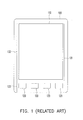
- Fig. 1 is a schematic diagram showing a conventional electronic device 100.
- the electronic device 100 is a touch-sensitive device, such as a smart phone, a personal digital assistant (PDA), a tablet personal computer (PC), a notebook PC, or a desktop PC.
- the electronic device 100 includes a touch display 110 and some virtual keys 120. Each virtual key 120 may detect touch operations of the user in the same way as the touch display 110 does.
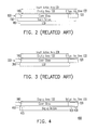
- Fig. 2 is a cross-sectional view showing the electronic device 100.
- the touch display 110 includes a cover glass 140, a touch sensor 150 and a liquid crystal module (LCM) 160.
- the size of the display area 132 is the same as the size of the cover glass 140 that exposes the images displayed by the LCM 160.
- the touch active area 131 is the touch-sensitive surface of the electronic device 100.
- the size of the touch active area 131 is the same as the size of the touch sensor 150.
- the touch sensor 150 extends beyond the cover glass 140 and the LCM 160 and extends under the virtual keys 120. Therefore, the touch active area 131 covers the display area 132 and the virtual key area 133.
- the user may make selections by simply touching the display area 132 or the virtual key area 133 via a finger or stylus.
- the electronic device 100 may recognize the positions of touch events induced by the user on the touch active area 131 by scanning the touch sensor 150 and then perform actions based on the touch events.
- the touch sensor 150 and the LCM 160 are separate components. Since fabrication technology is always getting improved, there is always a trend of integrating related components into a single one to reduce complexity and cost of the entire system. Recently, the in-cell and on-cell technology enable the integration of the touch sensor and the LCM.
- Fig. 3 is a cross-sectional view showing another conventional touch-sensitive electronic device 300.
- the integrated LCM 360 in the electronic device 300 replaces the touch sensor 150 and the LCM 160 in the electronic device 100.
- the touch active area 331 of the electronic device 300 covers the display area 132.
- the virtual keys 120 of the electronic device 300 cannot work because there is no touch sensor under them.
- the present invention is directed to an electronic device.
- the electronic device includes an integrated display module and an independent touch sensor.
- the integrated display module may be used for detecting touch operations on the touch display and the independent touch sensor may be used for detecting touch operations on the virtual keys.
- Such a touch-sensing device provides a low-cost solution to increase the effectiveness, efficiency and user satisfaction with touch-sensitive electronic devices.
- the present invention is also directed to a touch-sensing method.
- the touch-sensing method increases the effectiveness, efficiency and user satisfaction with touch-sensitive electronic devices in the same way as that of the aforementioned touch-sensing electronic device.
- an electronic device includes an display module integrated with a first touch sensor, a second touch sensor, and a sense circuitry.
- the display module may be a liquid crystal module (LCM).
- the first touch sensor generates a first sensing signal in response to a first driving signal.
- the second touch sensor generates a second sensing signal in response to a second driving signal.
- the sense circuitry is coupled to the first and the second touch sensors. The sense circuitry receives and analyzes the first sensing signal and the second sensing signal.
- a touch-sensing method includes the following steps. Provide a first driving signal to a first touch sensor integrated with an display module, or instruct the first driving signal to be provided to the first touch sensor. Provide a second driving signal to a second touch sensor. Receive and analyze a first sensing signal generated by the first touch sensor in response to the first driving signal. Receive and analyze a second sensing signal generated by the second touch sensor in response to the second driving signal.
- Fig. 1 is a schematic diagram showing a conventional touch-sensitive electronic device.
- Fig. 2 and Fig. 3 are cross-sectional views showing conventional touch-sensitive electronic devices.
- Fig. 4 is a cross-sectional view showing a part of a touch-sensitive electronic device according to an embodiment of the present invention.
- Fig. 5 is a schematic diagram showing a part of a touch-sensitive electronic device according to an embodiment of the present invention.
- Fig. 6 is a schematic diagram showing a part of a touch-sensitive electronic device according to an embodiment of the present invention.
- Fig. 7 is a schematic diagram showing a part of a touch-sensitive electronic device according to another embodiment of the present invention.
- Fig. 8 is a schematic diagram showing the flow of a touch-sensing method according to an embodiment of the present invention.
- Fig. 4 is a cross-sectional view showing a part of a touch-sensitive electronic device 400 according to an embodiment of the present invention.
- the electronic device 400 may be a smart phone, a PDA, a tablet PC, a notebook PC, or a desktop PC.
- the electronic device 400 includes a cover glass 140, an integrated display module 410, an touch sensor 415 integrated with the display module 410, a virtual key touch sensor 420, a light guide 430 under the virtual key touch sensor 420, and some virtual keys 120.
- the touch sensor 415 may be an in-cell touch sensor or an on-cell touch sensor.
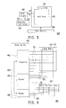
- Fig. 5 is a schematic diagram showing a part of the touch-sensitive electronic device 400 according to an embodiment of the present invention.
- the electronic device 400 includes the display module 410 integrated with the touch sensor 415, the virtual key touch sensor 420, a sense circuitry 440 and a drive circuitry 550.
- the sense circuitry 440 may be a touch controller and the drive circuitry 550 may be an LCM driver.
- the sense circuitry 440 is coupled to the touch sensors 415 and 420.
- the drive circuitry 550 is coupled to the display module 410.
- the display module 410 may be a liquid crystal module (LCM), light-emitting diode (LED) module or organic light-emitting diode (OLED) module.
- LCD liquid crystal module
- LED light-emitting diode
- OLED organic light-emitting diode
- the sense circuitry 440 detects touch events in the display area 132 by scanning the touch sensor 415. In order to scan the touch sensor 415, the sense circuitry 440 provides the driving signal 511 to the touch sensor 415. The touch sensor 415 generates the sensing signal 515 in response to the driving signal 511. The sense circuitry 440 receives and analyzes the sensing signal 515 in order to recognize the positions of the touch events in the display area 132. Similarly, the sense circuitry 440 detects touch events in the virtual key area 133 by scanning the virtual key touch sensor 420. In order to scan the virtual key touch sensor 420, the sense circuitry 440 provides the virtual key driving signal 521 to the virtual key touch sensor 420.
- the virtual key touch sensor 420 generates the virtual key sensing signal 525 in response to the virtual key driving signal 521.
- the sense circuitry 440 receives and analyzes the virtual key sensing signal 525 in order to recognize the positions of the touch events in the virtual key area 133.
- the electronic device 400 may perform functions based on the locations of the touch events detected by the sense circuitry 440.
- the drive circuitry 550 drives the display module 410 to display an image, such as the graphical user interface (GUI) of the electronic device 400.
- GUI graphical user interface
- the touch sensors 415 and 420, the sense circuitry 440 and the drive circuitry 550 are physical circuits.
- the sense circuitry 440 may provide the display module driving signal 511 to the touch sensor 415 according to a first timing.
- the sense circuitry 440 may provide the virtual key driving signal 521 to the virtual key touch sensor 420 according to a second timing.
- the first timing and the second timing are different. In other words, the sense circuitry 440 does not output the driving signal 511 and the virtual key driving signal 521 at the same moment. Therefore, the scanning of the touch sensor 415 does not interfere with the scanning of the virtual key touch sensor 420.
- the sense circuitry 440 may provide the driving signal 511 to the touch sensor 415 at a first frequency.
- the sense circuitry 440 may provide the virtual key driving signal 521 to the virtual key touch sensor 420 at a second frequency.
- the first frequency and the second frequency are different. Since the sense circuitry 440 outputs the driving signal 511 and the virtual key driving signal 521 at different frequencies, the scanning of the touch sensor 415 does not interfere with the scanning of the virtual key touch sensor 420.
- the sense circuitry 440 may simultaneously send the driving signal 511 and the virtual key driving signal 521 through the same output terminal to the touch sensor 415 and the virtual key touch sensor 420, respectively.
- the sense circuitry 440 may send out the driving signal 511 and the virtual key driving signal 521 at different frequencies to avoid interference.
- Fig. 6 is a schematic diagram showing the display module 410, the touch sensor 415, the virtual key touch sensor 420, and the sense circuitry 440 in the electronic device 400.
- the sense circuitry 440 includes a transmitter 442 and two receivers 444 and 446.
- the receiver 444 is coupled to the touch sensor 415 for receiving the sensing signal 515
- the receiver 446 is coupled to the virtual key touch sensor 420 for receiving the virtual key sensing signal 525.
- the transmitter 442 is coupled to the touch sensor 415, the virtual key touch sensor 420, and the receivers 444 and 446.
- the transmitter 442 sends the driving signal 511 to the touch sensor 415 and sends a control signal 450 to trigger the receiver 444 to receive the sensing signal 515.
- the transmitter 442 sends the virtual key driving signal 521 to the virtual key touch sensor 420 and sends the control signal 450 to trigger the receiver 446 to receive the virtual key sensing signal 525.
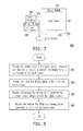
- Fig. 7 is a schematic diagram showing a part of the touch-sensitive electronic device 400 according to another embodiment of the present invention.
- the touch-sensitive electronic device 400 includes an display module 410, an touch sensor 415 integrated with the display module 410, a virtual key touch sensor 420, a sense circuitry 760 coupled to the sensor 415 and the virtual key touch sensor 420, and a drive circuitry 750 coupled to the display module 410, the touch sensor 415, and the sense circuitry 760.
- the drive circuitry 750 drives the display module 410 to display an image, such as the GUI of the electronic device 400.
- the sense circuitry 760 and the drive circuitry 750 are both physical circuits.
- the sense circuitry 760 instructs the drive circuitry 750 to provide the driving signal 511 to the touch sensor 415 and the sense circuitry 760 provides the virtual key driving signal 521 to the virtual key touch sensor 420.
- the touch sensor 415 generates the sensing signal 515 in response to the driving signal 511.
- the sense circuitry 760 receives the analyzes the sensing signal 515 and determines the locations of the touch events in the display area 132 based on the analysis of the sensing signal 515.
- the virtual key touch sensor 420 generates the virtual key sensing signal 525 in response to the virtual key driving signal 521.
- the sense circuitry 760 receives the analyzes the virtual key sensing signal 525 and determines the locations of the touch events in the virtual key area 133 based on the analysis of the virtual key sensing signal 525.
- the electronic device 400 may perform functions based on the locations of the touch events detected by the sense circuitry 760.
- sense circuitry the sense circuitry 760 may instruct the drive circuitry 750 to provide the driving signal 511 to the touch sensor 415 according to a first timing.
- the sense circuitry may provide the virtual key driving signal 521 to the virtual key touch sensor 420 according to a second timing.
- the first timing and the second timing are different such that the scanning of the touch sensor 415 does not interfere with the scanning of the virtual key touch sensor 420.
- the sense circuitry 760 may instruct the drive circuitry 750 to provide the driving signal 511 to the touch sensor 415 at a first frequency.
- the sense circuitry may provide the virtual key driving signal 521 to the virtual key touch sensor 420 at a second frequency.
- the first frequency and the second frequency are different such that the scanning of the touch sensor 415 does not interfere with the scanning of the virtual key touch sensor 420.
- Fig. 8 is a schematic diagram showing the flow of a touch-sensing method according to an embodiment of the present invention.
- the touch-sensing method includes the following steps, which may be executed by the touch-sensing electronic device 400 shown in Fig. 5, Fig. 6 or Fig. 7 .
- step 810 provide the driving signal 511 to the touch sensor 415 integrated with the display module 410, or instruct the driving signal 511 to be provided to the touch sensor 415.
- step 820 provide the virtual key driving signal 521 to the virtual key touch sensor 420.
- step 830 receive and analyze the sensing signal 515 generated by the touch sensor 415 in response to the driving signal 511.
- step 840 receive and analyze the virtual key sensing signal 525 generated by the virtual key touch sensor 420 in response to the virtual key driving signal 521.
- the aforementioned embodiments of the present invention scan the touch sensor and the virtual key touch sensor by receiving and analyzing the sensing signal and the virtual key sensing signal respectively.
- the present invention is not limited to the touch sensor and the virtual key touch sensor.
- the other embodiments of the present invention may scan a plurality of arbitrary touch sensors by receiving and analyzing their sensing signals respectively.
- the present invention uses a single sense circuitry to scan at least two touch sensors.
- One of the touch sensors may be used to detect touch events in the display area of an electronic device.
- the other one of the touch sensors may be used to detect touch events in the virtual key area of the electronic device.
- the present invention reduces the cost and complexity of the electronic device.
- the present invention may increase the effectiveness, efficiency and user satisfaction with touch-sensitive electronic devices by using a stand-alone touch sensor to detect touch events on the virtual keys.
Landscapes
- Engineering & Computer Science (AREA)
- Theoretical Computer Science (AREA)
- General Engineering & Computer Science (AREA)
- Physics & Mathematics (AREA)
- General Physics & Mathematics (AREA)
- Human Computer Interaction (AREA)
- Computer Hardware Design (AREA)
- Computer Networks & Wireless Communication (AREA)
- Signal Processing (AREA)
- Position Input By Displaying (AREA)
- Electronic Switches (AREA)
- User Interface Of Digital Computer (AREA)
Abstract
Description
- This application claims the priority benefits of
U.S. provisional application serial no. 61/546,069, filed on October 12, 2011 - The present invention relates to an electronic device and a touch-sensing method. More particularly, the present invention relates to an electronic device and a method of sensing touch operations on two touch sensors.
-
Fig. 1 is a schematic diagram showing a conventionalelectronic device 100. Theelectronic device 100 is a touch-sensitive device, such as a smart phone, a personal digital assistant (PDA), a tablet personal computer (PC), a notebook PC, or a desktop PC. Theelectronic device 100 includes atouch display 110 and somevirtual keys 120. Eachvirtual key 120 may detect touch operations of the user in the same way as thetouch display 110 does. -
Fig. 2 is a cross-sectional view showing theelectronic device 100. Thetouch display 110 includes acover glass 140, atouch sensor 150 and a liquid crystal module (LCM) 160. The size of thedisplay area 132 is the same as the size of thecover glass 140 that exposes the images displayed by the LCM 160. The touchactive area 131 is the touch-sensitive surface of theelectronic device 100. The size of the touchactive area 131 is the same as the size of thetouch sensor 150. Thetouch sensor 150 extends beyond thecover glass 140 and the LCM 160 and extends under thevirtual keys 120. Therefore, the touchactive area 131 covers thedisplay area 132 and thevirtual key area 133. The user may make selections by simply touching thedisplay area 132 or thevirtual key area 133 via a finger or stylus. In general, theelectronic device 100 may recognize the positions of touch events induced by the user on the touchactive area 131 by scanning thetouch sensor 150 and then perform actions based on the touch events. - In
Fig. 2 , thetouch sensor 150 and theLCM 160 are separate components. Since fabrication technology is always getting improved, there is always a trend of integrating related components into a single one to reduce complexity and cost of the entire system. Recently, the in-cell and on-cell technology enable the integration of the touch sensor and the LCM. - For example,
Fig. 3 is a cross-sectional view showing another conventional touch-sensitiveelectronic device 300. The integratedLCM 360 in theelectronic device 300 replaces thetouch sensor 150 and theLCM 160 in theelectronic device 100. There is a touch sensor (not shown) integrated with the LCM 360. However, since the touch sensor integrated with the LCM 360 has the same size as that of the LCM 360, the touchactive area 331 of theelectronic device 300 covers thedisplay area 132. Thevirtual keys 120 of theelectronic device 300 cannot work because there is no touch sensor under them. - Accordingly, the present invention is directed to an electronic device. The electronic device includes an integrated display module and an independent touch sensor. The integrated display module may be used for detecting touch operations on the touch display and the independent touch sensor may be used for detecting touch operations on the virtual keys. Such a touch-sensing device provides a low-cost solution to increase the effectiveness, efficiency and user satisfaction with touch-sensitive electronic devices.
- The present invention is also directed to a touch-sensing method. The touch-sensing method increases the effectiveness, efficiency and user satisfaction with touch-sensitive electronic devices in the same way as that of the aforementioned touch-sensing electronic device.
- According to an embodiment of the present invention, an electronic device is provided. The electronic device includes an display module integrated with a first touch sensor, a second touch sensor, and a sense circuitry. The display module may be a liquid crystal module (LCM). The first touch sensor generates a first sensing signal in response to a first driving signal. The second touch sensor generates a second sensing signal in response to a second driving signal. The sense circuitry is coupled to the first and the second touch sensors. The sense circuitry receives and analyzes the first sensing signal and the second sensing signal.
- According to another embodiment of the present invention, a touch-sensing method is provided, which includes the following steps. Provide a first driving signal to a first touch sensor integrated with an display module, or instruct the first driving signal to be provided to the first touch sensor. Provide a second driving signal to a second touch sensor. Receive and analyze a first sensing signal generated by the first touch sensor in response to the first driving signal. Receive and analyze a second sensing signal generated by the second touch sensor in response to the second driving signal.
- The accompanying drawings are included to provide a further understanding of the invention, and are incorporated in and constitute a part of this specification. The drawings illustrate embodiments of the invention and, together with the description, serve to explain the principles of the invention.
-
Fig. 1 is a schematic diagram showing a conventional touch-sensitive electronic device. -
Fig. 2 and Fig. 3 are cross-sectional views showing conventional touch-sensitive electronic devices. -
Fig. 4 is a cross-sectional view showing a part of a touch-sensitive electronic device according to an embodiment of the present invention. -
Fig. 5 is a schematic diagram showing a part of a touch-sensitive electronic device according to an embodiment of the present invention. -
Fig. 6 is a schematic diagram showing a part of a touch-sensitive electronic device according to an embodiment of the present invention. -
Fig. 7 is a schematic diagram showing a part of a touch-sensitive electronic device according to another embodiment of the present invention. -
Fig. 8 is a schematic diagram showing the flow of a touch-sensing method according to an embodiment of the present invention. - Reference will now be made in detail to the present embodiments of the invention, examples of which are illustrated in the accompanying drawings. Wherever possible, the same reference numbers are used in the drawings and the description to refer to the same or like parts.
-
Fig. 4 is a cross-sectional view showing a part of a touch-sensitiveelectronic device 400 according to an embodiment of the present invention. Theelectronic device 400 may be a smart phone, a PDA, a tablet PC, a notebook PC, or a desktop PC. Theelectronic device 400 includes acover glass 140, an integrateddisplay module 410, antouch sensor 415 integrated with thedisplay module 410, a virtualkey touch sensor 420, alight guide 430 under the virtualkey touch sensor 420, and somevirtual keys 120. Thetouch sensor 415 may be an in-cell touch sensor or an on-cell touch sensor. -
Fig. 5 is a schematic diagram showing a part of the touch-sensitiveelectronic device 400 according to an embodiment of the present invention. Theelectronic device 400 includes thedisplay module 410 integrated with thetouch sensor 415, the virtualkey touch sensor 420, asense circuitry 440 and adrive circuitry 550. Thesense circuitry 440 may be a touch controller and thedrive circuitry 550 may be an LCM driver. Thesense circuitry 440 is coupled to thetouch sensors drive circuitry 550 is coupled to thedisplay module 410. Thedisplay module 410 may be a liquid crystal module (LCM), light-emitting diode (LED) module or organic light-emitting diode (OLED) module. - The
sense circuitry 440 detects touch events in thedisplay area 132 by scanning thetouch sensor 415. In order to scan thetouch sensor 415, thesense circuitry 440 provides the drivingsignal 511 to thetouch sensor 415. Thetouch sensor 415 generates thesensing signal 515 in response to thedriving signal 511. Thesense circuitry 440 receives and analyzes thesensing signal 515 in order to recognize the positions of the touch events in thedisplay area 132. Similarly, thesense circuitry 440 detects touch events in the virtualkey area 133 by scanning the virtualkey touch sensor 420. In order to scan the virtualkey touch sensor 420, thesense circuitry 440 provides the virtualkey driving signal 521 to the virtualkey touch sensor 420. The virtualkey touch sensor 420 generates the virtualkey sensing signal 525 in response to the virtualkey driving signal 521. Thesense circuitry 440 receives and analyzes the virtualkey sensing signal 525 in order to recognize the positions of the touch events in the virtualkey area 133. Theelectronic device 400 may perform functions based on the locations of the touch events detected by thesense circuitry 440. Thedrive circuitry 550 drives thedisplay module 410 to display an image, such as the graphical user interface (GUI) of theelectronic device 400. Thetouch sensors sense circuitry 440 and thedrive circuitry 550 are physical circuits. - In an embodiment of the present invention, the
sense circuitry 440 may provide the displaymodule driving signal 511 to thetouch sensor 415 according to a first timing. Thesense circuitry 440 may provide the virtualkey driving signal 521 to the virtualkey touch sensor 420 according to a second timing. The first timing and the second timing are different. In other words, thesense circuitry 440 does not output the drivingsignal 511 and the virtualkey driving signal 521 at the same moment. Therefore, the scanning of thetouch sensor 415 does not interfere with the scanning of the virtualkey touch sensor 420. - In another embodiment of the present invention, the
sense circuitry 440 may provide thedriving signal 511 to thetouch sensor 415 at a first frequency. Thesense circuitry 440 may provide the virtualkey driving signal 521 to the virtualkey touch sensor 420 at a second frequency. The first frequency and the second frequency are different. Since thesense circuitry 440 outputs thedriving signal 511 and the virtualkey driving signal 521 at different frequencies, the scanning of thetouch sensor 415 does not interfere with the scanning of the virtualkey touch sensor 420. - In still another embodiment of the present invention, the
sense circuitry 440 may simultaneously send thedriving signal 511 and the virtualkey driving signal 521 through the same output terminal to thetouch sensor 415 and the virtualkey touch sensor 420, respectively. Thesense circuitry 440 may send out the drivingsignal 511 and the virtualkey driving signal 521 at different frequencies to avoid interference. -
Fig. 6 is a schematic diagram showing thedisplay module 410, thetouch sensor 415, the virtualkey touch sensor 420, and thesense circuitry 440 in theelectronic device 400. Thesense circuitry 440 includes atransmitter 442 and tworeceivers receiver 444 is coupled to thetouch sensor 415 for receiving thesensing signal 515, while thereceiver 446 is coupled to the virtualkey touch sensor 420 for receiving the virtualkey sensing signal 525. Thetransmitter 442 is coupled to thetouch sensor 415, the virtualkey touch sensor 420, and thereceivers transmitter 442 sends the drivingsignal 511 to thetouch sensor 415 and sends acontrol signal 450 to trigger thereceiver 444 to receive thesensing signal 515. In addition, thetransmitter 442 sends the virtualkey driving signal 521 to the virtualkey touch sensor 420 and sends thecontrol signal 450 to trigger thereceiver 446 to receive the virtualkey sensing signal 525. -
Fig. 7 is a schematic diagram showing a part of the touch-sensitiveelectronic device 400 according to another embodiment of the present invention. In this embodiment, the touch-sensitiveelectronic device 400 includes andisplay module 410, antouch sensor 415 integrated with thedisplay module 410, a virtualkey touch sensor 420, asense circuitry 760 coupled to thesensor 415 and the virtualkey touch sensor 420, and adrive circuitry 750 coupled to thedisplay module 410, thetouch sensor 415, and thesense circuitry 760. Thedrive circuitry 750 drives thedisplay module 410 to display an image, such as the GUI of theelectronic device 400. Thesense circuitry 760 and thedrive circuitry 750 are both physical circuits. - In order to scan the
touch sensor 415 and the virtualkey touch sensor 420 to detect touch events, thesense circuitry 760 instructs thedrive circuitry 750 to provide thedriving signal 511 to thetouch sensor 415 and thesense circuitry 760 provides the virtualkey driving signal 521 to the virtualkey touch sensor 420. Thetouch sensor 415 generates thesensing signal 515 in response to thedriving signal 511. Thesense circuitry 760 receives the analyzes thesensing signal 515 and determines the locations of the touch events in thedisplay area 132 based on the analysis of thesensing signal 515. On the other hand, the virtualkey touch sensor 420 generates the virtualkey sensing signal 525 in response to the virtualkey driving signal 521. Thesense circuitry 760 receives the analyzes the virtualkey sensing signal 525 and determines the locations of the touch events in the virtualkey area 133 based on the analysis of the virtualkey sensing signal 525. Theelectronic device 400 may perform functions based on the locations of the touch events detected by thesense circuitry 760. - In an embodiment of the present invention,sense circuitry the
sense circuitry 760 may instruct thedrive circuitry 750 to provide thedriving signal 511 to thetouch sensor 415 according to a first timing. The sense circuitry may provide the virtualkey driving signal 521 to the virtualkey touch sensor 420 according to a second timing. The first timing and the second timing are different such that the scanning of thetouch sensor 415 does not interfere with the scanning of the virtualkey touch sensor 420. - In another embodiment of the present invention, the
sense circuitry 760 may instruct thedrive circuitry 750 to provide thedriving signal 511 to thetouch sensor 415 at a first frequency. The sense circuitry may provide the virtualkey driving signal 521 to the virtualkey touch sensor 420 at a second frequency. The first frequency and the second frequency are different such that the scanning of thetouch sensor 415 does not interfere with the scanning of the virtualkey touch sensor 420. -
Fig. 8 is a schematic diagram showing the flow of a touch-sensing method according to an embodiment of the present invention. The touch-sensing method includes the following steps, which may be executed by the touch-sensingelectronic device 400 shown inFig. 5, Fig. 6 orFig. 7 . Instep 810, provide thedriving signal 511 to thetouch sensor 415 integrated with thedisplay module 410, or instruct thedriving signal 511 to be provided to thetouch sensor 415. Instep 820, provide the virtualkey driving signal 521 to the virtualkey touch sensor 420. Instep 830, receive and analyze thesensing signal 515 generated by thetouch sensor 415 in response to thedriving signal 511. Instep 840, receive and analyze the virtualkey sensing signal 525 generated by the virtualkey touch sensor 420 in response to the virtualkey driving signal 521. - The other details of the touch-sensing method are already elaborated on in the aforementioned embodiments of the present invention. Therefore, the details are not repeated here.
- The aforementioned embodiments of the present invention scan the touch sensor and the virtual key touch sensor by receiving and analyzing the sensing signal and the virtual key sensing signal respectively. The present invention is not limited to the touch sensor and the virtual key touch sensor. The other embodiments of the present invention may scan a plurality of arbitrary touch sensors by receiving and analyzing their sensing signals respectively.
- In summary, the present invention uses a single sense circuitry to scan at least two touch sensors. One of the touch sensors may be used to detect touch events in the display area of an electronic device. The other one of the touch sensors may be used to detect touch events in the virtual key area of the electronic device. By using a single sense circuitry instead of two sense circuitrys, the present invention reduces the cost and complexity of the electronic device. In addition, the present invention may increase the effectiveness, efficiency and user satisfaction with touch-sensitive electronic devices by using a stand-alone touch sensor to detect touch events on the virtual keys.
- It will be apparent to those skilled in the art that various modifications and variations may be made to the structure of the present invention without departing from the scope or spirit of the invention. In view of the foregoing, it is intended that the present invention cover modifications and variations of this invention provided they fall within the scope of the following claims and their equivalents.
Claims (15)
- An electronic device, comprising:a display module integrated with a first touch sensor, wherein the first touch sensor generates a first sensing signal in response to a first driving signal;a second touch sensor, generating a second sensing signal in response to a second driving signal; anda sense circuitry, coupled to the first and the second touch sensors, receiving and analyzing the first sensing signal and the second sensing signal.
- The electronic device of claim 1, wherein the sense circuitry provides the first driving signal to the first touch sensor according to a first frequency and provides the second driving signal to the second touch sensor according to a second frequency, the first frequency and the second frequency are different.
- The electronic device of any of claims 1-2, wherein the sense circuitry simultaneously sends the first and the second driving signals through a same output terminal to the first and the second touch sensors, respectively.
- The electronic device of any of claims 1-3, wherein the sense circuitry comprises:a first receiver coupled to the first touch sensor, receiving the first sensing signal;a second receiver coupled to the second touch sensor, receiving the second sensing signal; anda transmitter coupled to the first and the second touch sensors and the first and the second receivers, sending the first driving signal to the first touch sensor and sending a control signal to trigger the first receiver to receive the first sensing signal, sending the second driving signal to the second touch sensor and sending the control signal to trigger the second receiver to receive the second sensing signal.
- The electronic device of any of claims 1-4, further comprising:a drive circuitry, coupled to the display module, driving the display module to display an image.
- The electronic device of claim 5, wherein the sense circuitry instructs the drive circuitry to provide the first driving signal to the first touch sensor according to a first frequency, the sense circuitry provides the second driving signal to the second touch sensor according to a second frequency, the first frequency and the second frequency are different.
- A touch-sensing method, comprising:providing a first driving signal to a first touch sensor integrated with a display module, or instructing the first driving signal to be provided to the first touch sensor;providing a second driving signal to a second touch sensor;receiving and analyzing a first sensing signal generated by the first touch sensor in response to the first driving signal; andreceiving and analyzing a second sensing signal generated by the second touch sensor in response to the second driving signal.
- The touch-sensing method of claim 7, furthering comprising:providing the first driving signal to the first touch sensor according to a first timing; andproviding the second driving signal to the second touch sensor according to a second timing, wherein the first timing and the second timing are different.
- The touch-sensing method of any of claims 7-8, furthering comprising:providing the first driving signal to the first touch sensor according to a first frequency; andproviding the second driving signal to the second touch sensor according to a second frequency, wherein the first frequency and the second frequency are different.
- The touch-sensing method of any of claims 7-9, further comprising:simultaneously sending the first and the second driving signals through a same output terminal to the first and the second touch sensors, respectively.
- The touch-sensing method of any of claims 7-10, further comprising:sending the first driving signal to the first touch sensor and sending a control signal to trigger the receiving of the first sensing signal; andsending the second driving signal to the second touch sensor and sending the control signal to trigger the receiving of the second sensing signal.
- The touch-sensing method of any of claims 7-11, further comprising:driving the display module to display an image by a drive circuitry.
- The touch-sensing method of claim 12, further comprising:instructing the drive circuitry to provide the first driving signal to the first touch sensor according to a first timing; andproviding the second driving signal to the second touch sensor according to a second timing, wherein the first timing and the second timing are different.
- The touch-sensing method of any of claims 12-13, further comprising:instructing the drive circuitry to provide the first driving signal to the first touch sensor according to a first frequency; andproviding the second driving signal to the second touch sensor according to a second frequency, wherein the first frequency and the second frequency are different.
- An apparatus operative to perform the method of any of the claims 7-14.
Applications Claiming Priority (2)
| Application Number | Priority Date | Filing Date | Title |
|---|---|---|---|
| US201161546069P | 2011-10-12 | 2011-10-12 | |
| US13/606,026 US9298304B2 (en) | 2011-10-12 | 2012-09-07 | Electronic device and touch-sensing method |
Publications (3)
| Publication Number | Publication Date |
|---|---|
| EP2581813A2 true EP2581813A2 (en) | 2013-04-17 |
| EP2581813A3 EP2581813A3 (en) | 2014-10-15 |
| EP2581813B1 EP2581813B1 (en) | 2016-04-13 |
Family
ID=47257331
Family Applications (1)
| Application Number | Title | Priority Date | Filing Date |
|---|---|---|---|
| EP12007053.7A Active EP2581813B1 (en) | 2011-10-12 | 2012-10-11 | Electronic device and touch-sensing method |
Country Status (6)
| Country | Link |
|---|---|
| US (1) | US9298304B2 (en) |
| EP (1) | EP2581813B1 (en) |
| JP (1) | JP5727981B2 (en) |
| KR (1) | KR101427858B1 (en) |
| CN (1) | CN103049129A (en) |
| TW (1) | TWI494800B (en) |
Cited By (1)
| Publication number | Priority date | Publication date | Assignee | Title |
|---|---|---|---|---|
| FR3009099A1 (en) * | 2013-07-26 | 2015-01-30 | Thales Sa | TOUCH-CAPACITIVE MULTI-TOUCH SURFACE DEVICE |
Families Citing this family (7)
| Publication number | Priority date | Publication date | Assignee | Title |
|---|---|---|---|---|
| CN103345316A (en) * | 2013-06-14 | 2013-10-09 | 业成光电(深圳)有限公司 | Electronic device with touch control function |
| CN103941905B (en) * | 2013-06-28 | 2017-03-29 | 上海天马微电子有限公司 | Embedded touch panel |
| TWI622837B (en) * | 2013-10-24 | 2018-05-01 | 元太科技工業股份有限公司 | Display apparatus |
| TWI603236B (en) * | 2014-02-19 | 2017-10-21 | 友達光電股份有限公司 | Touch panel, touch display panel and touch signal sensing method |
| WO2015129112A1 (en) * | 2014-02-28 | 2015-09-03 | 凸版印刷株式会社 | Lcd device |
| CN105981030A (en) * | 2016-04-12 | 2016-09-28 | 深圳信炜科技有限公司 | Electronic equipment |
| CN108108055B (en) * | 2018-01-02 | 2021-11-16 | 联想(北京)有限公司 | Touch device, touch method and electronic equipment |
Family Cites Families (22)
| Publication number | Priority date | Publication date | Assignee | Title |
|---|---|---|---|---|
| JPH06160118A (en) | 1992-11-26 | 1994-06-07 | Rika Kogyo Kk | Liquid crystal display device with touch switch |
| JP3368627B2 (en) | 1993-08-31 | 2003-01-20 | 双葉電子工業株式会社 | Display integrated tablet |
| US20030067447A1 (en) * | 2001-07-09 | 2003-04-10 | Geaghan Bernard O. | Touch screen with selective touch sources |
| TWM246655U (en) | 2003-08-20 | 2004-10-11 | Compal Electronics Inc | Mobile electronic device |
| CN101017419B (en) | 2005-06-30 | 2010-05-12 | 智点科技(深圳)有限公司 | Touch control panel display |
| TWI369534B (en) | 2008-02-26 | 2012-08-01 | Wintek Corp | Touch display, liquid crystal display with a built-in touch panel and fabricating method thereof |
| JP4816668B2 (en) | 2008-03-28 | 2011-11-16 | ソニー株式会社 | Display device with touch sensor |
| US8368657B2 (en) | 2008-12-01 | 2013-02-05 | Freescale Semiconductor, Inc. | Touch sensor panel using regional and local electrodes to increase number of sense locations |
| KR101365792B1 (en) | 2009-04-28 | 2014-02-20 | 닛본 덴끼 가부시끼가이샤 | Touch panel, touch panel manufacturing method, and electronic apparatus |
| JP2011002926A (en) | 2009-06-17 | 2011-01-06 | Hitachi Ltd | Display device with tactile exhibition function |
| TWI448930B (en) | 2009-08-12 | 2014-08-11 | Innolux Corp | Touch display |
| KR101309862B1 (en) | 2009-12-10 | 2013-09-16 | 엘지디스플레이 주식회사 | Liquid Crystal Display Device Including Touch Panel |
| KR20110081040A (en) | 2010-01-06 | 2011-07-13 | 삼성전자주식회사 | Method and device for operating contents in portable terminal with transparent display |
| US9786254B2 (en) * | 2010-02-26 | 2017-10-10 | Synaptics Incorporated | Sensing during non-display update time to avoid interference |
| JP5382658B2 (en) | 2010-02-26 | 2014-01-08 | 株式会社ジャパンディスプレイ | Display device with touch sensor, touch panel, touch panel driving method, and electronic device |
| JP2011198009A (en) * | 2010-03-19 | 2011-10-06 | Sony Corp | Electro-optical device with input function |
| TWI435140B (en) | 2010-04-09 | 2014-04-21 | Wintek Corp | Display with touch panel |
| TW201142777A (en) * | 2010-05-28 | 2011-12-01 | Au Optronics Corp | Sensing display panel |
| US8451250B2 (en) | 2010-07-22 | 2013-05-28 | Au Optronics Corporation | Capacitive touch device and method of driving same |
| JP5539106B2 (en) * | 2010-08-23 | 2014-07-02 | 株式会社ジャパンディスプレイ | Display device with touch detection function, drive circuit, driving method of display device with touch detection function, and electronic device |
| KR101394937B1 (en) * | 2010-09-07 | 2014-05-15 | 엘지디스플레이 주식회사 | Display device having touch sensor and method for driving the same |
| US20130069894A1 (en) * | 2011-09-16 | 2013-03-21 | Htc Corporation | Electronic device and method for driving a touch sensor thereof |
-
2012
- 2012-09-07 US US13/606,026 patent/US9298304B2/en active Active
- 2012-09-18 KR KR1020120103123A patent/KR101427858B1/en active Active
- 2012-10-02 JP JP2012220579A patent/JP5727981B2/en active Active
- 2012-10-05 TW TW101136944A patent/TWI494800B/en active
- 2012-10-11 EP EP12007053.7A patent/EP2581813B1/en active Active
- 2012-10-12 CN CN2012103853789A patent/CN103049129A/en active Pending
Non-Patent Citations (1)
| Title |
|---|
| None |
Cited By (1)
| Publication number | Priority date | Publication date | Assignee | Title |
|---|---|---|---|---|
| FR3009099A1 (en) * | 2013-07-26 | 2015-01-30 | Thales Sa | TOUCH-CAPACITIVE MULTI-TOUCH SURFACE DEVICE |
Also Published As
| Publication number | Publication date |
|---|---|
| KR101427858B1 (en) | 2014-08-08 |
| US9298304B2 (en) | 2016-03-29 |
| TWI494800B (en) | 2015-08-01 |
| EP2581813A3 (en) | 2014-10-15 |
| EP2581813B1 (en) | 2016-04-13 |
| JP5727981B2 (en) | 2015-06-03 |
| CN103049129A (en) | 2013-04-17 |
| TW201316221A (en) | 2013-04-16 |
| JP2013084268A (en) | 2013-05-09 |
| US20130093701A1 (en) | 2013-04-18 |
Similar Documents
| Publication | Publication Date | Title |
|---|---|---|
| US9298304B2 (en) | Electronic device and touch-sensing method | |
| JP6052743B2 (en) | Touch panel device and control method of touch panel device | |
| US9507521B2 (en) | Input apparatus, input mode switching method and computer apparatus | |
| EP2597552B1 (en) | Touch screen and multi-channel sampling method thereof | |
| US20110260987A1 (en) | Dual screen electronic device | |
| KR102120930B1 (en) | User input method of portable device and the portable device enabling the method | |
| CN102119376B (en) | Multidimensional Navigation for Touch-Sensitive Displays | |
| CN112416157A (en) | Control circuit and method for controlling display screen | |
| US9035914B2 (en) | Touch system including optical touch panel and touch pen, and method of controlling interference optical signal in touch system | |
| US20130314377A1 (en) | Optical touch sensor apparatus | |
| CN103105983B (en) | Method and apparatus for improving the touch sensitivity of touch panel | |
| US10606418B2 (en) | Ultrasonic touch detection on stylus | |
| CN105453006B (en) | Gesture sensitive display | |
| WO2019047744A1 (en) | Liquid crystal screen module and display terminal | |
| US20120075217A1 (en) | Object sensing device | |
| US10775926B2 (en) | Method of performing touch sensing and fingerprint sensing simultaneously and electronic device and system using the same | |
| KR200477008Y1 (en) | Smart phone with mouse module | |
| KR20150020865A (en) | Method and apparatus for processing a input of electronic device | |
| US10191584B2 (en) | Reducing connections from a sensing module | |
| KR20140130798A (en) | Apparatus and method for touch screen panel display and touch key | |
| US20140372915A1 (en) | Method and system for operating display device | |
| US20120169666A1 (en) | Optical touch-sensing liquid crystal panel, optical touch-sensing panel and method of determining touch position | |
| US20150169103A1 (en) | Touch display apparatus | |
| JP2013114645A (en) | Small information device | |
| KR101961786B1 (en) | Method and apparatus for providing function of mouse using terminal including touch screen |
Legal Events
| Date | Code | Title | Description |
|---|---|---|---|
| PUAI | Public reference made under article 153(3) epc to a published international application that has entered the european phase |
Free format text: ORIGINAL CODE: 0009012 |
|
| 17P | Request for examination filed |
Effective date: 20121011 |
|
| AK | Designated contracting states |
Kind code of ref document: A2 Designated state(s): AL AT BE BG CH CY CZ DE DK EE ES FI FR GB GR HR HU IE IS IT LI LT LU LV MC MK MT NL NO PL PT RO RS SE SI SK SM TR |
|
| AX | Request for extension of the european patent |
Extension state: BA ME |
|
| PUAL | Search report despatched |
Free format text: ORIGINAL CODE: 0009013 |
|
| AK | Designated contracting states |
Kind code of ref document: A3 Designated state(s): AL AT BE BG CH CY CZ DE DK EE ES FI FR GB GR HR HU IE IS IT LI LT LU LV MC MK MT NL NO PL PT RO RS SE SI SK SM TR |
|
| AX | Request for extension of the european patent |
Extension state: BA ME |
|
| RIC1 | Information provided on ipc code assigned before grant |
Ipc: G06F 3/0488 20130101ALI20140911BHEP Ipc: G06F 3/041 20060101AFI20140911BHEP |
|
| 17Q | First examination report despatched |
Effective date: 20140929 |
|
| RAP1 | Party data changed (applicant data changed or rights of an application transferred) |
Owner name: HTC CORPORATION |
|
| RBV | Designated contracting states (corrected) |
Designated state(s): AL AT BE BG CH CY CZ DE DK EE ES FI FR GB GR HR HU IE IS IT LI LT LU LV MC MK MT NL NO PL PT RO RS SE SI SK SM TR |
|
| GRAP | Despatch of communication of intention to grant a patent |
Free format text: ORIGINAL CODE: EPIDOSNIGR1 |
|
| INTG | Intention to grant announced |
Effective date: 20151022 |
|
| GRAS | Grant fee paid |
Free format text: ORIGINAL CODE: EPIDOSNIGR3 |
|
| GRAA | (expected) grant |
Free format text: ORIGINAL CODE: 0009210 |
|
| AK | Designated contracting states |
Kind code of ref document: B1 Designated state(s): AL AT BE BG CH CY CZ DE DK EE ES FI FR GB GR HR HU IE IS IT LI LT LU LV MC MK MT NL NO PL PT RO RS SE SI SK SM TR |
|
| REG | Reference to a national code |
Ref country code: GB Ref legal event code: FG4D |
|
| REG | Reference to a national code |
Ref country code: AT Ref legal event code: REF Ref document number: 790798 Country of ref document: AT Kind code of ref document: T Effective date: 20160415 Ref country code: CH Ref legal event code: EP |
|
| REG | Reference to a national code |
Ref country code: IE Ref legal event code: FG4D |
|
| REG | Reference to a national code |
Ref country code: DE Ref legal event code: R096 Ref document number: 602012016943 Country of ref document: DE |
|
| REG | Reference to a national code |
Ref country code: NL Ref legal event code: FP |
|
| REG | Reference to a national code |
Ref country code: LT Ref legal event code: MG4D |
|
| REG | Reference to a national code |
Ref country code: AT Ref legal event code: MK05 Ref document number: 790798 Country of ref document: AT Kind code of ref document: T Effective date: 20160413 |
|
| REG | Reference to a national code |
Ref country code: FR Ref legal event code: PLFP Year of fee payment: 5 |
|
| PG25 | Lapsed in a contracting state [announced via postgrant information from national office to epo] |
Ref country code: LT Free format text: LAPSE BECAUSE OF FAILURE TO SUBMIT A TRANSLATION OF THE DESCRIPTION OR TO PAY THE FEE WITHIN THE PRESCRIBED TIME-LIMIT Effective date: 20160413 Ref country code: FI Free format text: LAPSE BECAUSE OF FAILURE TO SUBMIT A TRANSLATION OF THE DESCRIPTION OR TO PAY THE FEE WITHIN THE PRESCRIBED TIME-LIMIT Effective date: 20160413 Ref country code: PL Free format text: LAPSE BECAUSE OF FAILURE TO SUBMIT A TRANSLATION OF THE DESCRIPTION OR TO PAY THE FEE WITHIN THE PRESCRIBED TIME-LIMIT Effective date: 20160413 Ref country code: NO Free format text: LAPSE BECAUSE OF FAILURE TO SUBMIT A TRANSLATION OF THE DESCRIPTION OR TO PAY THE FEE WITHIN THE PRESCRIBED TIME-LIMIT Effective date: 20160713 |
|
| PG25 | Lapsed in a contracting state [announced via postgrant information from national office to epo] |
Ref country code: SE Free format text: LAPSE BECAUSE OF FAILURE TO SUBMIT A TRANSLATION OF THE DESCRIPTION OR TO PAY THE FEE WITHIN THE PRESCRIBED TIME-LIMIT Effective date: 20160413 Ref country code: AT Free format text: LAPSE BECAUSE OF FAILURE TO SUBMIT A TRANSLATION OF THE DESCRIPTION OR TO PAY THE FEE WITHIN THE PRESCRIBED TIME-LIMIT Effective date: 20160413 Ref country code: HR Free format text: LAPSE BECAUSE OF FAILURE TO SUBMIT A TRANSLATION OF THE DESCRIPTION OR TO PAY THE FEE WITHIN THE PRESCRIBED TIME-LIMIT Effective date: 20160413 Ref country code: RS Free format text: LAPSE BECAUSE OF FAILURE TO SUBMIT A TRANSLATION OF THE DESCRIPTION OR TO PAY THE FEE WITHIN THE PRESCRIBED TIME-LIMIT Effective date: 20160413 Ref country code: GR Free format text: LAPSE BECAUSE OF FAILURE TO SUBMIT A TRANSLATION OF THE DESCRIPTION OR TO PAY THE FEE WITHIN THE PRESCRIBED TIME-LIMIT Effective date: 20160714 Ref country code: LV Free format text: LAPSE BECAUSE OF FAILURE TO SUBMIT A TRANSLATION OF THE DESCRIPTION OR TO PAY THE FEE WITHIN THE PRESCRIBED TIME-LIMIT Effective date: 20160413 Ref country code: ES Free format text: LAPSE BECAUSE OF FAILURE TO SUBMIT A TRANSLATION OF THE DESCRIPTION OR TO PAY THE FEE WITHIN THE PRESCRIBED TIME-LIMIT Effective date: 20160413 Ref country code: PT Free format text: LAPSE BECAUSE OF FAILURE TO SUBMIT A TRANSLATION OF THE DESCRIPTION OR TO PAY THE FEE WITHIN THE PRESCRIBED TIME-LIMIT Effective date: 20160816 |
|
| PG25 | Lapsed in a contracting state [announced via postgrant information from national office to epo] |
Ref country code: BE Free format text: LAPSE BECAUSE OF FAILURE TO SUBMIT A TRANSLATION OF THE DESCRIPTION OR TO PAY THE FEE WITHIN THE PRESCRIBED TIME-LIMIT Effective date: 20160413 Ref country code: IT Free format text: LAPSE BECAUSE OF FAILURE TO SUBMIT A TRANSLATION OF THE DESCRIPTION OR TO PAY THE FEE WITHIN THE PRESCRIBED TIME-LIMIT Effective date: 20160413 |
|
| REG | Reference to a national code |
Ref country code: DE Ref legal event code: R097 Ref document number: 602012016943 Country of ref document: DE |
|
| PG25 | Lapsed in a contracting state [announced via postgrant information from national office to epo] |
Ref country code: EE Free format text: LAPSE BECAUSE OF FAILURE TO SUBMIT A TRANSLATION OF THE DESCRIPTION OR TO PAY THE FEE WITHIN THE PRESCRIBED TIME-LIMIT Effective date: 20160413 Ref country code: RO Free format text: LAPSE BECAUSE OF FAILURE TO SUBMIT A TRANSLATION OF THE DESCRIPTION OR TO PAY THE FEE WITHIN THE PRESCRIBED TIME-LIMIT Effective date: 20160413 Ref country code: SK Free format text: LAPSE BECAUSE OF FAILURE TO SUBMIT A TRANSLATION OF THE DESCRIPTION OR TO PAY THE FEE WITHIN THE PRESCRIBED TIME-LIMIT Effective date: 20160413 Ref country code: CZ Free format text: LAPSE BECAUSE OF FAILURE TO SUBMIT A TRANSLATION OF THE DESCRIPTION OR TO PAY THE FEE WITHIN THE PRESCRIBED TIME-LIMIT Effective date: 20160413 Ref country code: DK Free format text: LAPSE BECAUSE OF FAILURE TO SUBMIT A TRANSLATION OF THE DESCRIPTION OR TO PAY THE FEE WITHIN THE PRESCRIBED TIME-LIMIT Effective date: 20160413 |
|
| PLBE | No opposition filed within time limit |
Free format text: ORIGINAL CODE: 0009261 |
|
| STAA | Information on the status of an ep patent application or granted ep patent |
Free format text: STATUS: NO OPPOSITION FILED WITHIN TIME LIMIT |
|
| PG25 | Lapsed in a contracting state [announced via postgrant information from national office to epo] |
Ref country code: SM Free format text: LAPSE BECAUSE OF FAILURE TO SUBMIT A TRANSLATION OF THE DESCRIPTION OR TO PAY THE FEE WITHIN THE PRESCRIBED TIME-LIMIT Effective date: 20160413 |
|
| 26N | No opposition filed |
Effective date: 20170116 |
|
| PG25 | Lapsed in a contracting state [announced via postgrant information from national office to epo] |
Ref country code: SI Free format text: LAPSE BECAUSE OF FAILURE TO SUBMIT A TRANSLATION OF THE DESCRIPTION OR TO PAY THE FEE WITHIN THE PRESCRIBED TIME-LIMIT Effective date: 20160413 |
|
| REG | Reference to a national code |
Ref country code: CH Ref legal event code: PL |
|
| REG | Reference to a national code |
Ref country code: IE Ref legal event code: MM4A |
|
| PG25 | Lapsed in a contracting state [announced via postgrant information from national office to epo] |
Ref country code: CH Free format text: LAPSE BECAUSE OF NON-PAYMENT OF DUE FEES Effective date: 20161031 Ref country code: LI Free format text: LAPSE BECAUSE OF NON-PAYMENT OF DUE FEES Effective date: 20161031 |
|
| PG25 | Lapsed in a contracting state [announced via postgrant information from national office to epo] |
Ref country code: LU Free format text: LAPSE BECAUSE OF NON-PAYMENT OF DUE FEES Effective date: 20161011 |
|
| REG | Reference to a national code |
Ref country code: FR Ref legal event code: PLFP Year of fee payment: 6 |
|
| PG25 | Lapsed in a contracting state [announced via postgrant information from national office to epo] |
Ref country code: IE Free format text: LAPSE BECAUSE OF NON-PAYMENT OF DUE FEES Effective date: 20161011 |
|
| PG25 | Lapsed in a contracting state [announced via postgrant information from national office to epo] |
Ref country code: HU Free format text: LAPSE BECAUSE OF FAILURE TO SUBMIT A TRANSLATION OF THE DESCRIPTION OR TO PAY THE FEE WITHIN THE PRESCRIBED TIME-LIMIT; INVALID AB INITIO Effective date: 20121011 Ref country code: CY Free format text: LAPSE BECAUSE OF FAILURE TO SUBMIT A TRANSLATION OF THE DESCRIPTION OR TO PAY THE FEE WITHIN THE PRESCRIBED TIME-LIMIT Effective date: 20160413 |
|
| PG25 | Lapsed in a contracting state [announced via postgrant information from national office to epo] |
Ref country code: TR Free format text: LAPSE BECAUSE OF FAILURE TO SUBMIT A TRANSLATION OF THE DESCRIPTION OR TO PAY THE FEE WITHIN THE PRESCRIBED TIME-LIMIT Effective date: 20160413 Ref country code: MT Free format text: LAPSE BECAUSE OF NON-PAYMENT OF DUE FEES Effective date: 20161031 Ref country code: MC Free format text: LAPSE BECAUSE OF FAILURE TO SUBMIT A TRANSLATION OF THE DESCRIPTION OR TO PAY THE FEE WITHIN THE PRESCRIBED TIME-LIMIT Effective date: 20160413 Ref country code: MK Free format text: LAPSE BECAUSE OF FAILURE TO SUBMIT A TRANSLATION OF THE DESCRIPTION OR TO PAY THE FEE WITHIN THE PRESCRIBED TIME-LIMIT Effective date: 20160413 Ref country code: IS Free format text: LAPSE BECAUSE OF FAILURE TO SUBMIT A TRANSLATION OF THE DESCRIPTION OR TO PAY THE FEE WITHIN THE PRESCRIBED TIME-LIMIT Effective date: 20160413 |
|
| PG25 | Lapsed in a contracting state [announced via postgrant information from national office to epo] |
Ref country code: BG Free format text: LAPSE BECAUSE OF FAILURE TO SUBMIT A TRANSLATION OF THE DESCRIPTION OR TO PAY THE FEE WITHIN THE PRESCRIBED TIME-LIMIT Effective date: 20160413 |
|
| REG | Reference to a national code |
Ref country code: FR Ref legal event code: PLFP Year of fee payment: 7 |
|
| PG25 | Lapsed in a contracting state [announced via postgrant information from national office to epo] |
Ref country code: AL Free format text: LAPSE BECAUSE OF FAILURE TO SUBMIT A TRANSLATION OF THE DESCRIPTION OR TO PAY THE FEE WITHIN THE PRESCRIBED TIME-LIMIT Effective date: 20160413 |
|
| P01 | Opt-out of the competence of the unified patent court (upc) registered |
Effective date: 20230602 |
|
| PGFP | Annual fee paid to national office [announced via postgrant information from national office to epo] |
Ref country code: NL Payment date: 20250912 Year of fee payment: 14 |
|
| PGFP | Annual fee paid to national office [announced via postgrant information from national office to epo] |
Ref country code: GB Payment date: 20250904 Year of fee payment: 14 |
|
| PGFP | Annual fee paid to national office [announced via postgrant information from national office to epo] |
Ref country code: FR Payment date: 20250908 Year of fee payment: 14 |
|
| PGFP | Annual fee paid to national office [announced via postgrant information from national office to epo] |
Ref country code: DE Payment date: 20250902 Year of fee payment: 14 |