EP2580583B1 - Three-dimensional hot spot localization - Google Patents
Three-dimensional hot spot localization Download PDFInfo
- Publication number
- EP2580583B1 EP2580583B1 EP11741492.0A EP11741492A EP2580583B1 EP 2580583 B1 EP2580583 B1 EP 2580583B1 EP 11741492 A EP11741492 A EP 11741492A EP 2580583 B1 EP2580583 B1 EP 2580583B1
- Authority
- EP
- European Patent Office
- Prior art keywords
- sample
- thermal
- lock
- depth
- frequency
- Prior art date
- Legal status (The legal status is an assumption and is not a legal conclusion. Google has not performed a legal analysis and makes no representation as to the accuracy of the status listed.)
- Active
Links
Images


Classifications
-
- G—PHYSICS
- G01—MEASURING; TESTING
- G01N—INVESTIGATING OR ANALYSING MATERIALS BY DETERMINING THEIR CHEMICAL OR PHYSICAL PROPERTIES
- G01N25/00—Investigating or analyzing materials by the use of thermal means
- G01N25/72—Investigating presence of flaws
-
- G—PHYSICS
- G01—MEASURING; TESTING
- G01J—MEASUREMENT OF INTENSITY, VELOCITY, SPECTRAL CONTENT, POLARISATION, PHASE OR PULSE CHARACTERISTICS OF INFRARED, VISIBLE OR ULTRAVIOLET LIGHT; COLORIMETRY; RADIATION PYROMETRY
- G01J5/00—Radiation pyrometry, e.g. infrared or optical thermometry
- G01J5/0066—Radiation pyrometry, e.g. infrared or optical thermometry for hot spots detection
-
- G—PHYSICS
- G01—MEASURING; TESTING
- G01R—MEASURING ELECTRIC VARIABLES; MEASURING MAGNETIC VARIABLES
- G01R31/00—Arrangements for testing electric properties; Arrangements for locating electric faults; Arrangements for electrical testing characterised by what is being tested not provided for elsewhere
- G01R31/28—Testing of electronic circuits, e.g. by signal tracer
- G01R31/302—Contactless testing
- G01R31/308—Contactless testing using non-ionising electromagnetic radiation, e.g. optical radiation
- G01R31/311—Contactless testing using non-ionising electromagnetic radiation, e.g. optical radiation of integrated circuits
-
- G—PHYSICS
- G01—MEASURING; TESTING
- G01N—INVESTIGATING OR ANALYSING MATERIALS BY DETERMINING THEIR CHEMICAL OR PHYSICAL PROPERTIES
- G01N1/00—Sampling; Preparing specimens for investigation
-
- G—PHYSICS
- G01—MEASURING; TESTING
- G01N—INVESTIGATING OR ANALYSING MATERIALS BY DETERMINING THEIR CHEMICAL OR PHYSICAL PROPERTIES
- G01N21/00—Investigating or analysing materials by the use of optical means, i.e. using sub-millimetre waves, infrared, visible or ultraviolet light
- G01N21/84—Systems specially adapted for particular applications
- G01N21/88—Investigating the presence of flaws or contamination
-
- G—PHYSICS
- G01—MEASURING; TESTING
- G01N—INVESTIGATING OR ANALYSING MATERIALS BY DETERMINING THEIR CHEMICAL OR PHYSICAL PROPERTIES
- G01N25/00—Investigating or analyzing materials by the use of thermal means
-
- G—PHYSICS
- G01—MEASURING; TESTING
- G01J—MEASUREMENT OF INTENSITY, VELOCITY, SPECTRAL CONTENT, POLARISATION, PHASE OR PULSE CHARACTERISTICS OF INFRARED, VISIBLE OR ULTRAVIOLET LIGHT; COLORIMETRY; RADIATION PYROMETRY
- G01J5/00—Radiation pyrometry, e.g. infrared or optical thermometry
- G01J2005/0077—Imaging
-
- G—PHYSICS
- G01—MEASURING; TESTING
- G01J—MEASUREMENT OF INTENSITY, VELOCITY, SPECTRAL CONTENT, POLARISATION, PHASE OR PULSE CHARACTERISTICS OF INFRARED, VISIBLE OR ULTRAVIOLET LIGHT; COLORIMETRY; RADIATION PYROMETRY
- G01J5/00—Radiation pyrometry, e.g. infrared or optical thermometry
- G01J5/48—Thermography; Techniques using wholly visual means
- G01J5/485—Temperature profile
-
- G—PHYSICS
- G01—MEASURING; TESTING
- G01N—INVESTIGATING OR ANALYSING MATERIALS BY DETERMINING THEIR CHEMICAL OR PHYSICAL PROPERTIES
- G01N21/00—Investigating or analysing materials by the use of optical means, i.e. using sub-millimetre waves, infrared, visible or ultraviolet light
- G01N21/84—Systems specially adapted for particular applications
- G01N2021/8461—Investigating impurities in semiconductor, e.g. Silicon
-
- G—PHYSICS
- G01—MEASURING; TESTING
- G01N—INVESTIGATING OR ANALYSING MATERIALS BY DETERMINING THEIR CHEMICAL OR PHYSICAL PROPERTIES
- G01N21/00—Investigating or analysing materials by the use of optical means, i.e. using sub-millimetre waves, infrared, visible or ultraviolet light
- G01N21/17—Systems in which incident light is modified in accordance with the properties of the material investigated
- G01N21/25—Colour; Spectral properties, i.e. comparison of effect of material on the light at two or more different wavelengths or wavelength bands
- G01N21/31—Investigating relative effect of material at wavelengths characteristic of specific elements or molecules, e.g. atomic absorption spectrometry
- G01N21/35—Investigating relative effect of material at wavelengths characteristic of specific elements or molecules, e.g. atomic absorption spectrometry using infrared light
Definitions
- the invention relates to three dimensional localization of resistive heat sources (hot spots) buried inside of electronic devices.
- Standard failure localization methods like OBIRCH or Emission Microscopy can mostly not be applied since the optical access to buried electronic structures within the 3D architecture is limited by opaque material layers. This is most critical in case of 3D system in package devices due to the fact that thermal active structures and defects can be buried at deeper dies or interconnect levels covered by opaque die attach, redistribution or encapsulation layers. Separation of individual dies for separate failure analysis may be an option to localize defects but this process is very time consuming and can come with a high risk of creating additional preparation-related defects reducing significantly the failure analysis success rate.
- LIT refers to a non destructive technique that detect very small temperature variations across a sample by direct thermal imaging, using an IR sensitive camera combined with pixel-wise two channel lock in correlation, LIT provides ⁇ m spatial resolution and ⁇ K sensitivity to locate thermal active structures and defects in x and y coordinates, but until now doesn't enable depth localization.
- thermal time delay is proportional to the phase signal and can be measured by two channel lock-in thermography, which allows a recalculation of the heat source distance to the surface and therefore its depth within or under the material layer.
- the Pulse Phase Thermography can detect sub-surface delaminations, material impurities, voids, etc. It can be used for contactless detection of weak welding joints (see, e.g., Thermosensorik, of Germany). In comparison to LIT, thermal pulse absorption is less sensitive and provides less spatial resolution.
- US 6 812 468 B1 teaches thermal wave measuring methods for contact-free measurement of geometrical or thermal features of a planar multi-layer structure, whereby simultaneous multi-frequency excitation with two or more discrete frequencies of an electrically modulatable hot light source enables the parallel evaluation corresponding to the different drive frequencies.
- the measuring time in the measurement of multi-layer Systems is significantly shortened.
- the discrete frequency parts of the drive frequencies these can be adapted to the measurement problem.
- Dillenz et al. ("Progress in phase angle thermography," Review of Scientific Instruments, vol. 74, no. 1, 1 January 2003, pages 417-419 ) teaches nondestructive and reliable evaluation of samples by lock-in-thermography using multi-frequency excitation, thereby allowing for depth profiling from one measurement.
- Liu et al. (“Effect of modulation frequency on detecting defects of metal plates using infrared lock-in thermography," Proceedings of SPIE - The International Symposium on Advanced Optical Manufacturing and Testing Technologies: Optical Test and Measurement Technology and Equipment 2009, vol. 7283, pages 72833M-1 to 72833M-7, 19 November 2008 ) discusses detection of defects in the subsurface of metal plates using lock-in thermography (LIT).
- LIT lock-in thermography
- the invention is directed to a method an a system for detecting the location of buried heat sources using lock-in-thermography which allows fast and secure detection of the thermally active structure.
- the method of the invention comprises the features of claim 1 and the system of the invention comprises the features of claim 13.
- Preferred embodiments are characterized in the sub-claims.
- LIT Lock-in Thermography
- the positions of hot spots can be located and pinpointed in all three dimensions by analyzing the thermal heat propagation through defect-covering layers utilizing lock in amplified thermal imaging.
- the invention in particular enables a non destructive 3D localization of thermal active structures or defects in a vertical stack of integrated circuits and interconnect layers within system in package devices (SiP).
- aspects of the invention provide three-dimensional allocation of buried hot spots based on phase and time-resolved thermal response measurements by means of lock-in thermography.
- a method is disclosed to discriminate one, or multiple thermal active structures, which can be stimulated by applying an electrical signal, out of numerous stacked layers by means of non-destructive measurements of the heat, generated at the thermal active structure inside of the stack and detected on the surface of the device.
- embodiments of this invention allow localizing the defective layer (die) through the encapsulation (including the full layer stack) by measuring and analyzing the phase shifts (in case of Lock-in Thermography) and/or the thermal time delays (in case of time-resolved thermal response measurements) as a function of the applied excitation frequency (lock-in frequency).
- DUT may be applicable to these devices as well.
- Three dimensional architectures of electronic devices e.g. system in packages (SiP) are composed of several integrated circuit dies, die attaches or interconnect redistribution layers stacked vertically and encapsulated together. Consequently, such encapsulated electronic devices are heterogenous material stacks containing silicon, polymer and Si-oxide isolators, metal lines and wires, glue and/or adhesives, encapsulation mould, etc. Therefore, the internal heat propagation starting from the hot spot position can be very complex. Consequently, location of a hot spot defect in the z direction, i.e., its depth within the sample, is difficult. Furthermore, complex defects or sample types may result in non-ideal hot spot activation in terms of power conversion at the hot spot location.
- Various embodiments disclosed herein enable accurate localization of heat sources (e.g. thermally active structures or defects) in such devices.
- Various embodiments of the invention use defined multiple frequencies for device excitation (primarily, but not exclusively square waves voltage signals with 50% duty cycle). Analysis of the resulting phase shift between excitation and thermal response vs. frequency curve enables the necessary hot spot depth calculation accuracy, including a comparison to simulated and/or pre-calibrated data. Time-resolved thermal response measurements (similar to the display of a thermal scope) are used to analyze the full thermal waveform for better accuracy with strongly reduced analysis time.
- Embodiments of the invention use quantitative measures for the phase shift/time delay between electrical stimulation and thermal response and the shape of the measured waveform for automated and semi-automated data analysis.
- the waveform shape analysis can be based on cross-correlation between the measured results and pre-defined functions (e.g. sine, cosine, shark-fin, triangle, square), delivering a correlation matrix rather than just single phase values per applied lock-in.
- the embodiments of the invention provide advantages such as: scanning the lock-in frequency offers measuring more data points and allows analyzing not only the individual absolute phase values, but also the shape/slope of the phase vs. frequency curve. This offers an well-defined phase shift/time delay measurement with increased detection accuracy and still allows 3D localization with non-ideal hot spot activation, where a single phase measurement would deliver wrong results. Also, the time resolved thermal response measurements can substantially reduce the necessary acquisition time per analyzed frequency by more than ten times, and potentially by up to 100 times. Furthermore, the gained full waveform allows further improved depth measurement accuracy, based on the quantitative analysis of the thermal time delay and the waveform shape. These improvements are expected to be necessary to resolve single layers in current and future multi layer electronic devices, i.e. 3D system in package technologies. The quantitative analysis of the thermal heat propagation allows for (semi) automated 3D allocation of hot spots.
- the main advantage of LIT in contrast to steady-state Thermography is the much higher sensitivity down to a few ⁇ W combined with higher spatial resolution down to a few ⁇ m.
- the device under test is periodically stimulated with a supply voltage by a chosen frequency (lock-in frequency).
- the resulting thermal response at the device surface is detected by an IR camera and split into an in-phase-part (S0°) and an out-of phase-part (S90°) related to the excitation signal by using two correlation functions.
- This process allows the calculation of amplitude and phase signal, which contain the necessary information for hot spot depth localization. Amplitude : S 0 ° + S 90 ° 2 Phase : arctan S 90 ° S 0 °
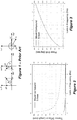
- the 0° and the 90° signals are plotted in a complex vector diagram, shown in Figure 1 .
- the resulting vector of both parts represents the amplitude A (arrow leading to point "S" in Figure 1 ) whereby the angle between 0° and the resulting amplitude vector is represented by the phase ⁇ .
- the phase value can be understood as a time delay between the excitation signal and the measured thermal response.
- thermal waves can propagate through this material, resulting in a periodically increased temperature at the device surface above the hot spot, which can be measured by LIT.
- the time constant of the underlying thermal diffusion process determines the phase shift between excitation signal and thermal response.
- the main contributors to the thermal delay are the material layers with less heat conductivity like mould compound, die attach glues, polymer and Si oxide isolators, but not the Si dies or metal layers which have a much higher heat conductivity.
- the longer the distance between hot spot and device surface the higher the resulting phase shift.
- knowing the thermal properties of the material above the hot spot allows the determination of an unknown depth of hot spots by measuring the phase shift.
- thermal diffusion length which describes the damping of the thermal wave inside the bulk material. It is defined as the characteristic length where the amplitude of the thermal wave is dropped down to e -1 . It can be calculated, as shown in equation 3, by the thermal parameters heat conductivity ( ⁇ in W/m*K), specific heat capacity (cp in J/g*K), density (p in g/cm 3 ) and the applied lock-in frequency ( f lock-in in Hz).
- the thermal diffusion length ⁇ (in mm) is characteristic for each material propagated by the thermal wave.
- Figure 2 shows the thermal diffusion length of two examples, mould compound (solid line) and silicon (dashed line). It can be observed that the thermal diffusion length of mould compound is significantly shorter compared to silicon. Furthermore it can be seen from Figure 2 that the lower the applied frequency is, the deeper the thermal wave propagates into the solid material. Consequently, reducing the frequency of the excitation signal allows the localization of heat sources even through hundreds of microns of IR-opaque material layers.
- the thermal diffusion length can be seen as the damping factor to the thermal wave, it affects not only the amplitude but also the resulting phase.
- a higher lock-in frequency results in a higher time delay between excitation signal at the hot spot position and the thermal response at the device surface. Therefore, an increase of the phase shift as a function of the increased lock-in frequency has to be expected.
- Figure 3 is a plot of the resulting phase shift as a function of the applied lock-in frequency for a hot spot buried under a one millimeter material layer. The solid line is a plot for the mould compound while the broken line is for the silicon.
- the detailed analysis of the internal heat propagation and the separation of different influences to the resulting phase shift is investigated using the method of finite element modelling.
- the modelling is used to simulate the lock-in process for a known device build up and defined hot spot positions.
- the heat transfer through a 3D system-in-package device can be done using 2D/3-D thermal modelling. Assuming different heat sources at different lateral and vertical positions inside of the device and correlating the resulting phase shifts for various lock in frequencies to the experimental data enables an identification of internal hot spot positions.
- the steady state solution that considers the transient response is calculated using half of the assumed dissipation power in order to reach a stable modulation within a few cycles.
- the sample is stimulated with the pulsed excitation signal.
- Lock-in frequency, number of excitation periods and number of intermediate steps are chosen with reference to the real geometries and thermal parameters (heat conductivity, heat capacity and density).
- the dissipation power is applied to the model ground and pulsed by various lock in frequencies.
- the time and power dissipation signals are saved in separate files, allowing the creation of the correlation functions and the reconstruction of the excitation signal. Two paths are created, where one is reading the temperature modulation over the surface and one over the thickness of the sample.
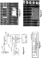
- FIG 4 is a diagram of a system according to an embodiment of the invention.
- DUT 400 is stimulated by excitation signal 430 at frequency f 0 generated by excitation source 405.
- the excitation signal 430 is a square wave having amplitude voltage equal to the DUT's operational voltage, e.g., 1.2 V, and a lock-in frequency f 0 .
- the frequency f 0 of the excitation signal is set and varied by frequency selector part 420, of processor 415.
- a sync signal 435 is output from the processor 415 and sent to the excitation source 405.
- the simplest is to set the sync signal 435 at the same frequency f 0 , although it may be a different frequency, so long as provisions are made to enable excitation source 405 to generate the excitation signal 430 at frequency f 0 .
- An IR camera 410 is used to snap IR images of selected area of the DUT 400.
- the frame rate of camera 410 is usually but not exclusively set to be higher than the frequency f 0 . Here it is set to at least four times higher than frequency f 0 .
- This operation can also be handled by an ATE, i.e., the ATE sends the drive signal to the DUT and at the same time sends a trigger signal to the controller and the camera.
- the DUT 400 is repeatedly excited by excitation source 405, while the frequency f 0 of the excitation signal is varied according to the sync signal 435 provided by the frequency selector 420.
- This enables a better and more accurate identification of a hot spot's location, especially its depth (i.e. z direction) within the electronic device.
- the setup of Figure 4 does not output a single phase data point, but rather enables plotting the entire response curve on monitor 425. Having the entire response curve enables further analysis, such as curve fitting to better understand the time-resolved heat dissipation within the DUT.
- the method of LIT can be used to non-destructively determine the hot spot position inside of a fully packaged single chip device providing a better alignment for the following physical failure analysis steps.
- the relationship between hot spot depth, applied lock-in frequency and resulting phase shift was investigated using test structures with defined point heat sources.
- the test structures were made using single chip device containing a meander of copper lines.
- the meander was locally modified by Focused Ion Beam technique (FIB), as shown in the upper part of Figure 5 to generate well-defined local heat sources.
- FIB Focused Ion Beam technique
- the device was encapsulated with mould compound in order to create a material layer between the FIB made hot spots and the device surface.
- the depth of the hot spots was known by the dimension of the device and the single chip and was determined at 950 ⁇ m.
- FIG. 7 shows a sketch of the investigated fully packaged test device.
- a dual ceramic in-line package (DCIP) houses the single chip with the created defect. Mould compound was filled over the chip, to thickness of 950 ⁇ m over the top surface of the chip.
- phase shift and lock-in frequency were determined experimentally for mold compound material with a good correlation to theoretical data. The obtained results are proving the potential of Lock-in Thermography investigations for 3D localization of thermal active structures or defects within fully package devices.
- the method of finite element modelling can be used simulating the lock-in process for a know device build up and a assumed defect position.
- the steady state solution that considers the transient response is calculated using half of the assumed dissipation power in order to reach a stabile modulation within a few cycles.
- the sample is simulated with the pulsed excitation signal. Lock-in frequency, number of excitation periods and number of intermediate steps are chosen with reference to the real parameters.
- the thermal parameters of the encapsulated material are considered and the dissipation power is applied to the model ground and pulsed by various lock in frequencies.
- the time and power dissipation signals are saved in separate files, allowing the creation of the correlation functions and the reconstruction of the excitation signal. Two paths are created, where one is reading the temperature modulation over the surface and one over the thickness of the sample.
- thermal waves generated at the hot spot position have to propagate through different material layers, e.g., silicon, mould compound, die attach tape, etc., each having different thicknesses.
- material layers e.g., silicon, mould compound, die attach tape, etc.
- thermal waves generated at hot spots at lower dies inside of the stack have to pass additional material layers compared to thermal waves generated at hot spots which are close to the device surface.
- the hot spot is related to a specific die, which leads to the circumstance that a discrete model of the material system can be used. Therefore, at least to a first order, the total thermal diffusion length is the summation of the single thermal diffusion length of each material layer. Also, the total depth z total of the hot spot is the summation of the thicknesses z n of the single material layers.
- the Lock-in process simulation is more complex using a 2D/3-D thermal model.
- the used stack materials silicon, stacked die glue, mould compound, copper
- their thermal parameters are applied. Assuming different heat sources at different lateral and vertical positions inside of the material stack and correlate the resulting theoretical phase shifts for various lock in frequencies to the experimental data indentifies the defect position.
- the phase shift related to the applied lock-in frequency was determined, which can be used as a reference of a defect located at the device surface.
- a bare silicon die with a thickness of 185 ⁇ m was attached at the surface of the prepared test chip using a die attach tape of 15 ⁇ m thickness, as shown in Figure 9B .
- the thermal properties of the die attach tape can be seen similar to mold compound. Therefore, the additional die attached layer is responsible for a higher resulting phase shift.
- the bare silicon chip should not contribute significantly to the change of the phase shift, because it is transparent for IR light and the thermal conductivity is much higher. This procedure was applied two more times, creating finally a stacked die device with three dies above the generated heat source structure, as shown in Figures 9C and 9D .
- phase shift under die 1+2 provide a good match with a theoretical phase shift for a frequency range of 0.1 to 3.
- Figure 11B is the phase results, representing the local thermal delay per pixel.
- the time-resolved thermal response analysis is based on measuring the necessary waveform by acquiring data in a very small window (e.g.
- the software can calculate the mean values across the small window or a subset (even smaller region) only covering the very center of the hot-spot at real time and averages the data, synchronized to the excitation (lock-in) frequency to generate the time-resolved thermal waveform (examples of such waveform are shown in figure 12 and 13 ).
- This process substantially increases the acquisition speed, since the SNR is based on the overall number of data points being averaged.
- the camera performs faster with reduced field of view (FOV), further increasing the acquisition by another 5 to 10 times (e.g. assuming 8).
- FOV field of view
- the reconstruction of a time-resolved waveform requires to average the incoming data separately, regarding their time of acquisition with respect to the excitation (lock-in) period.
- the time resolved waveform is obtained by plotting the thermal response of the device over time. This measurement is repeated for different lock-in frequencies.
- the shape of the time-resolved waveform obtained in different lock-in frequencies can be analyzed to determine the heat source's depth.
- the waveform can be cross-correlated to various functions, such as sine function, saw-tooth function, shark-fine function, etc.
- the waveform can also be correlated to a calibration data or to a library of waveforms. Cross-correlating the time-resolved waveform provides further depth information in addition to the phase shift.
- the initial image is taken using all of the pixels of the camera, e.g., 640x512 pixels of the sensor, e.g., InSb detector, as shown in Figure 11A .
- the image is projected on the monitor (425 in Figure 4 ) and the user is provided with a cursor to designate the location of the hot spot in x and y.
- the user may optionally also be provided with the ability to designate the size of the reduced field of view, e.g., select 16x16 pixels FOV.
- data is collected only from the designated field of view. For example, only the pixels corresponding to the 16x16 pixels are read at each cycle.
- the camera can be operated at a higher frame rate during the measurement process, thereby providing more data points for the averaging process.
- an IR sensor having a single pixel can be used.
- on-chip binning Another way to implement the reduced field of view imaging is by what's generally called on-chip binning.
- on-chip binning When on-chip binning is activated, the data from neighboring pixels are collected into a single data point. For example, if a 2x2 binning is activated, then the values of four neighboring pixels are added to generate a single readout. In this way, the camera can be operated at faster readout speeds and improved signal to noise ratios, albeit at the expense of reduced spatial resolution.
- the reduced spatial resolution of the binning process is irrelevant as the measurement is used only to determine the depth, not the spatial location.
- Figure 14 shows another time-resolved thermal response measurement, also showing the used lock-in voltage and a sin function, plotted for the delay yielding highest cross-correlation between the sin function and the thermal waveform.
- the cross-correlation allows to measure the thermal time delay ⁇ sin (measured between the rising edge of the lock-in voltage and the zero-point of the sin function) with higher accuracy compared to measuring at 50% of the temperature signal swing.
- embodiments of this invention enable the use of Lock-in Thermography for quantitative and non destructive 3D localization of hot spots i.e. generated by electrical structures or defects inside of electronic devices.
- the relationship between the applied lock-in frequency and the phase shift was determined based on the physical principles of thermal waves. This was done for the case where a hot spot is buried under a single material layer of unknown thickness and for the case of a hot spot buried under an unknown number of dies inside of a stacked die device. It was shown that buried hot spots even under a thick layer of mould compound can be localized in all three dimensions.
- Embodiments of the invention also enable the use of the time-resolved thermal response for more precise hot spot depth analysis, based on a point measurement. This allows decreasing the necessary measurement time substantially. Furthermore, it enables a more detailed data analysis of the shape of the acquired thermal waveform in addition to the thermal time delay.
Landscapes
- Physics & Mathematics (AREA)
- General Physics & Mathematics (AREA)
- Health & Medical Sciences (AREA)
- Engineering & Computer Science (AREA)
- Immunology (AREA)
- General Health & Medical Sciences (AREA)
- Pathology (AREA)
- Biochemistry (AREA)
- Analytical Chemistry (AREA)
- Chemical & Material Sciences (AREA)
- Life Sciences & Earth Sciences (AREA)
- Microelectronics & Electronic Packaging (AREA)
- General Engineering & Computer Science (AREA)
- Toxicology (AREA)
- Computer Vision & Pattern Recognition (AREA)
- Computer Hardware Design (AREA)
- Electromagnetism (AREA)
- Spectroscopy & Molecular Physics (AREA)
- Investigating Or Analyzing Materials Using Thermal Means (AREA)
- Radiation Pyrometers (AREA)
Description
- The invention relates to three dimensional localization of resistive heat sources (hot spots) buried inside of electronic devices.
- Failure analysis of modern complex system in package devices with a three-dimensional architecture is an increasing challenge. In such devices, several integrated circuit dies are vertically stacked and interconnected by wire bond or through silicon via (TSV) technologies. The access to and analysis of internal electronic structures or interconnects is limited to non destructive techniques, like magnetic microscopy, time domain reflectometry which can be used for signal tracking. Both methods are limited in resolution and the three dimensional positioning of electrical defects are very limited or extensive.
- Standard failure localization methods like OBIRCH or Emission Microscopy can mostly not be applied since the optical access to buried electronic structures within the 3D architecture is limited by opaque material layers. This is most critical in case of 3D system in package devices due to the fact that thermal active structures and defects can be buried at deeper dies or interconnect levels covered by opaque die attach, redistribution or encapsulation layers. Separation of individual dies for separate failure analysis may be an option to localize defects but this process is very time consuming and can come with a high risk of creating additional preparation-related defects reducing significantly the failure analysis success rate.
- Current localization techniques of thermal defects which can be electrically stimulated include the following:
- LIT refers to a non destructive technique that detect very small temperature variations across a sample by direct thermal imaging, using an IR sensitive camera combined with pixel-wise two channel lock in correlation, LIT provides µm spatial resolution and µK sensitivity to locate thermal active structures and defects in x and y coordinates, but until now doesn't enable depth localization.
- For a given thermal homogeneous material there is an approximately linear dependence between the depth of a heat source underneath the surface and the time it takes the heat to reach the surface. This thermal time delay is proportional to the phase signal and can be measured by two channel lock-in thermography, which allows a recalculation of the heat source distance to the surface and therefore its depth within or under the material layer.
- Conventional time-resolved temperature measurements allow to detect/display the thermal response of a sample with microsecond (µs) and milli-Kelvin (mK) accuracy.
- Based on pulsing heat onto a surface (backside or frontside) and measuring the temperature distribution/spreading in a time-resolved way. The Pulse Phase Thermography can detect sub-surface delaminations, material impurities, voids, etc. It can be used for contactless detection of weak welding joints (see, e.g., Thermosensorik, of Germany). In comparison to LIT, thermal pulse absorption is less sensitive and provides less spatial resolution.
- Schmidt et al. ("Application of Lock-in-Thermography for 3d defect localisation in complex devices," Electronics System Integration Technology Conference, 2008. ESTC 2008. 2ND, IEEE, Piscataway, NJ, USA, I-September-2008, pages 1041-1044) teaches measurement of defects in fully packaged devices using Lock-in-Thermography and shows, from experiments, that the lock-in-frequency has a significant influence to the size of the hot spot at the surface of the device and that for single chip devices an optimum frequency can be found depending on mold thickness above the inner heat source. This work further shows that the depth of failure can be determined by measuring the phase shift between electrical stimulation and thermal response at the device surface.
- Schmidt et al. ("Lock-in-thermography for 3-dimensional localization of electrical defects inside complex packaged devices," Conference Proceedings from The International Symposium for Testing and Failure Analysis (34th International Symposium for Testing and Failure Analysis, ISTFA) 2-November-2008 I-January-2008, pages 102-107) teaches the use of lock-in-thermography for non-destructive failure analysis of fully packaged single and multi-chip devices and demonstrates that the technique is sufficiently sensitive to enable measurement of temperature fields associated with inner hot spots. This paper further shows hot spots may be localized in three dimensions, with hot-spot depth determined by reassuring the phase shift between the electrical excitation and the thermal response at the device surface.
- Schmidt et al. ("Thermal Simulation of defect localisation using Lock-In Thermography in complex and fully packaged devices." 1 Oth International Conference on Thermal, Mechanical and Multi-Physics Simulation and Experiments in Microelectronics and Microsystems, 2009, EuroSimE. 26 April 2009, pages 1 -7) demonstrate that simulation of the lock-in process is possible and useful to withstand and optimize experimental results, the main advantage of such Simulation techniques being the possibility to investigate phase shift as a function of the distance through the device material and the possibility to determine the exact influence of each separate material layer thickness. In this paper, thermal spreading in lock-in processes are calculated using finite element modelling and compared with L1T measurements on test samples.
-
US 6 812 468 B1 teaches thermal wave measuring methods for contact-free measurement of geometrical or thermal features of a planar multi-layer structure, whereby simultaneous multi-frequency excitation with two or more discrete frequencies of an electrically modulatable hot light source enables the parallel evaluation corresponding to the different drive frequencies. As a result thereof, the measuring time in the measurement of multi-layer Systems is significantly shortened. As a result of a suitable selection of the discrete frequency parts of the drive frequencies, these can be adapted to the measurement problem. Dillenz et al. ("Progress in phase angle thermography," Review of Scientific Instruments, vol. 74, no. 1, 1 January 2003, pages 417-419) teaches nondestructive and reliable evaluation of samples by lock-in-thermography using multi-frequency excitation, thereby allowing for depth profiling from one measurement. - Tarin et al. ("Fuselage Inspection of Boeing-737 using Lock-in Thermography," Thermosense XXX, 18-March-2008, Orlando, FL USA, Proc. of SPIE Vol. 6939, 69393 9, 2008) teaches the use of multiple excitation in frequencies in lock-in thermography for analyzing complex structures, in particular, that the frequency of an applied Stimulus signal must be matched to the specific thermal conductivity and mass density of the inspected material.
- Liu et al. ("Effect of modulation frequency on detecting defects of metal plates using infrared lock-in thermography," Proceedings of SPIE - The International Symposium on Advanced Optical Manufacturing and Testing Technologies: Optical Test and Measurement Technology and Equipment 2009, vol. 7283, pages 72833M-1 to 72833M-7, 19 November 2008) discusses detection of defects in the subsurface of metal plates using lock-in thermography (LIT). This paper presents a heat conduction model to describe the transmitting process of sinusoidal (cosinusoidal) modulated heat flux in metal plates during infrared LIT and presents investigations into the effect of modulation frequency on detection depth/efficiency and the relationship between modulation frequency and phase difference. A range of modulation frequencies is obtained in which defects of all depth can clearly be detected.
- The following summary of the disclosure is included in order to provide a basic understanding of some aspects and features of the invention. This summary is not an extensive overview of the invention and as such it is not intended to particularly identify key or critical elements of the invention or to delineate the scope of the invention. Its sole purpose is to present some concepts of the invention in a simplified form as a prelude to the more detailed description that is presented below.
- The invention is directed to a method an a system for detecting the location of buried heat sources using lock-in-thermography which allows fast and secure detection of the thermally active structure.
- For this purpose, the method of the invention comprises the features of
claim 1 and the system of the invention comprises the features of claim 13. Preferred embodiments are characterized in the sub-claims. - A new approach for localization of heat sources in a non-destructive way by using Lock-in Thermography (LIT) is disclosed. The method of LIT is a very sensitive and easy to handle for hot spot detection and can be applied for the localization of die and packaging level defects. For quantitative LIT analysis and three dimensional allocation of buried heat sources, the basic principles of heat wave propagation, dependence of the thermal and geometrical properties of the material layer above the hot spot area, have to be understood.
- Using the described invention, the positions of hot spots can be located and pinpointed in all three dimensions by analyzing the thermal heat propagation through defect-covering layers utilizing lock in amplified thermal imaging. The invention in particular enables a non destructive 3D localization of thermal active structures or defects in a vertical stack of integrated circuits and interconnect layers within system in package devices (SiP).
- Aspects of the invention provide three-dimensional allocation of buried hot spots based on phase and time-resolved thermal response measurements by means of lock-in thermography. A method is disclosed to discriminate one, or multiple thermal active structures, which can be stimulated by applying an electrical signal, out of numerous stacked layers by means of non-destructive measurements of the heat, generated at the thermal active structure inside of the stack and detected on the surface of the device.
- The combination of Lock-in Thermography (fast localization of the hot spots in x and y) with time-resolved thermal response measurements at different excitation frequencies (for localization of the hot spots in the z direction) allows fast and secure detection of the thermally active structure.
- In addition to the non-destructive localization of thermal heat sources in x and y inside of fully packaged electronic devices, embodiments of this invention allow localizing the defective layer (die) through the encapsulation (including the full layer stack) by measuring and analyzing the phase shifts (in case of Lock-in Thermography) and/or the thermal time delays (in case of time-resolved thermal response measurements) as a function of the applied excitation frequency (lock-in frequency).
- While embodiments of the invention are described herein with respect to encapsulated integrated circuits, the invention can also be implemented for testing other devices that generate hot spots by electrical stimulation, such as batteries, solar cells, power devices, LED's, etc. Therefore, the term DUT may be applicable to these devices as well.
- Other aspects and features of the invention would be apparent from the detailed description, which is made with reference to the following drawings. It should be mentioned that the detailed description and the drawings provide various non-limiting examples of various embodiments of the invention, which is defined by the appended claims.
-
Figure 1 is a complex vector diagram, showing the basic LIT correlation signals (Real part and imaginary part) and in consequence the resulting amplitude vector and phase shift for an increasing distance of the defect position to the device surface, progressing from left to right. -
Figure 2 is a plot of thermal diffusion length as a function of the applied lock-in frequency for the materials silicon and mould compound. -
Figure 3 is a plot of the resulting phase shift as a function of the applied lock-in frequency resulting from an assumed defect under a one millimeter material layer of silicon and mould compound. -
Figure 4 is a diagram of a system according to an embodiment of the invention. -
Figure 5 is an image showing the creation of a localized defect using focused ion beam based circuit editing. -
Figure 6 is an image of the thermal intensity (Amplitude) overlaid over a topography image, showing the heat generated by the artificially generated defect (reference heat source) of the sample shown inFigure 5 . -
Figure 7 is a simplified sketch of one device under test. -
Figure 8 is a plot of experimental and theoretical phase shift related to the applied lock-in frequency. -
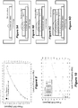
Figure 9A-9D are sketches of the experimental setup. -
Figure 10 is a plot of the experimental results of the investigated stacked device with different number of dies (DUT as shown infigure 9A-9D ). -
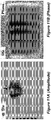
Figure 11A is a LIT results of overlay of topography and lock-in amplitude image, whileFigure 11B is the phase results. -
Figure 12 is a plot of time-resolved thermal response (similar to thermal waveforms); all measured with Vlockin = 1.2V, time of acquisition = 40sec, at full frame mode of camera (frame rate = 100Hz), for different lock-in frequencies. -
Figure 13 is a plot of time-resolved thermal response (similar to thermal waveforms); all measured with flockin = 1Hz, Vlockin = 1.2V, time of acquisition = 40sec, at different sub frame modes of camera (windowing, with higher frame rates). -
Figure 14 is a plot of time-resolved thermal response, measured with flockin = 1Hz, Vlockin = 1.2V, time of acquisition = 40sec, full frame mode (100Hz), with an overlay of the excitation/lock-in voltage and a sin function at the delay point of highest cross-correlation. The cross-correlation result can be used to determine the phase shift Δϕsin with increased accuracy. -
Figure 15 shows a time-resolved thermal response measured at 0.2 Hz (seeFigure 12 ) superimposed to the lock-in voltage, in comparison to different potential functions used for cross-correlation. Shown are a sin- a exponential charging and discharging- and a square-function, all resulting in different Δϕ and cross-correlation values. - Three dimensional architectures of electronic devices e.g. system in packages (SiP) are composed of several integrated circuit dies, die attaches or interconnect redistribution layers stacked vertically and encapsulated together. Consequently, such encapsulated electronic devices are heterogenous material stacks containing silicon, polymer and Si-oxide isolators, metal lines and wires, glue and/or adhesives, encapsulation mould, etc. Therefore, the internal heat propagation starting from the hot spot position can be very complex. Consequently, location of a hot spot defect in the z direction, i.e., its depth within the sample, is difficult. Furthermore, complex defects or sample types may result in non-ideal hot spot activation in terms of power conversion at the hot spot location. Various embodiments disclosed herein enable accurate localization of heat sources (e.g. thermally active structures or defects) in such devices.
- Various embodiments of the invention use defined multiple frequencies for device excitation (primarily, but not exclusively square waves voltage signals with 50% duty cycle). Analysis of the resulting phase shift between excitation and thermal response vs. frequency curve enables the necessary hot spot depth calculation accuracy, including a comparison to simulated and/or pre-calibrated data. Time-resolved thermal response measurements (similar to the display of a thermal scope) are used to analyze the full thermal waveform for better accuracy with strongly reduced analysis time.
- Embodiments of the invention use quantitative measures for the phase shift/time delay between electrical stimulation and thermal response and the shape of the measured waveform for automated and semi-automated data analysis. The waveform shape analysis can be based on cross-correlation between the measured results and pre-defined functions (e.g. sine, cosine, shark-fin, triangle, square), delivering a correlation matrix rather than just single phase values per applied lock-in.
- The embodiments of the invention provide advantages such as: scanning the lock-in frequency offers measuring more data points and allows analyzing not only the individual absolute phase values, but also the shape/slope of the phase vs. frequency curve. This offers an well-defined phase shift/time delay measurement with increased detection accuracy and still allows 3D localization with non-ideal hot spot activation, where a single phase measurement would deliver wrong results. Also, the time resolved thermal response measurements can substantially reduce the necessary acquisition time per analyzed frequency by more than ten times, and potentially by up to 100 times. Furthermore, the gained full waveform allows further improved depth measurement accuracy, based on the quantitative analysis of the thermal time delay and the waveform shape. These improvements are expected to be necessary to resolve single layers in current and future multi layer electronic devices, i.e. 3D system in package technologies. The quantitative analysis of the thermal heat propagation allows for (semi) automated 3D allocation of hot spots.
- The main advantage of LIT in contrast to steady-state Thermography is the much higher sensitivity down to a few µW combined with higher spatial resolution down to a few µm. In order to achieve these parameters the device under test is periodically stimulated with a supply voltage by a chosen frequency (lock-in frequency). The resulting thermal response at the device surface is detected by an IR camera and split into an in-phase-part (S0°) and an out-of phase-part (S90°) related to the excitation signal by using two correlation functions. This process allows the calculation of amplitude and phase signal, which contain the necessary information for hot spot depth localization.


- For a better understanding of the relationship between the basic signals (S0°, S90°) and the resulting amplitude and phase information, the 0° and the 90° signals are plotted in a complex vector diagram, shown in
Figure 1 . The resulting vector of both parts represents the amplitude A (arrow leading to point "S" inFigure 1 ) whereby the angle between 0° and the resulting amplitude vector is represented by the phase ϕ. The phase value can be understood as a time delay between the excitation signal and the measured thermal response. - In general, since the test is performed on devices with a material above the hot spot area is not transparent for the detected IR wavelength (typically but not exclusively 3-5um) thermal waves can propagate through this material, resulting in a periodically increased temperature at the device surface above the hot spot, which can be measured by LIT. The time constant of the underlying thermal diffusion process determines the phase shift between excitation signal and thermal response. The main contributors to the thermal delay are the material layers with less heat conductivity like mould compound, die attach glues, polymer and Si oxide isolators, but not the Si dies or metal layers which have a much higher heat conductivity. In simple terms, the longer the distance between hot spot and device surface, the higher the resulting phase shift. Reversely, knowing the thermal properties of the material above the hot spot, allows the determination of an unknown depth of hot spots by measuring the phase shift.
- The parameter which describes the influence of the thermal properties of a material layer is herein called thermal diffusion length (µ) which describes the damping of the thermal wave inside the bulk material. It is defined as the characteristic length where the amplitude of the thermal wave is dropped down to e-1. It can be calculated, as shown in
equation 3, by the thermal parameters heat conductivity (λ in W/m*K), specific heat capacity (cp in J/g*K), density (p in g/cm3) and the applied lock-in frequency (f lock-in in Hz). The thermal parameters can be summarized as the thermal diffusivity (a in mm2/s).
- The thermal diffusion length µ (in mm) is characteristic for each material propagated by the thermal wave.
Figure 2 shows the thermal diffusion length of two examples, mould compound (solid line) and silicon (dashed line). It can be observed that the thermal diffusion length of mould compound is significantly shorter compared to silicon. Furthermore it can be seen fromFigure 2 that the lower the applied frequency is, the deeper the thermal wave propagates into the solid material. Consequently, reducing the frequency of the excitation signal allows the localization of heat sources even through hundreds of microns of IR-opaque material layers. - Due to the fact that the thermal diffusion length can be seen as the damping factor to the thermal wave, it affects not only the amplitude but also the resulting phase. A higher lock-in frequency results in a higher time delay between excitation signal at the hot spot position and the thermal response at the device surface. Therefore, an increase of the phase shift as a function of the increased lock-in frequency has to be expected.
- The relationship between Phase ϕ and hot spot depth z is described as:

Figure 3 is a plot of the resulting phase shift as a function of the applied lock-in frequency for a hot spot buried under a one millimeter material layer. The solid line is a plot for the mould compound while the broken line is for the silicon. - According to one embodiment, the detailed analysis of the internal heat propagation and the separation of different influences to the resulting phase shift is investigated using the method of finite element modelling. The modelling is used to simulate the lock-in process for a known device build up and defined hot spot positions. The heat transfer through a 3D system-in-package device can be done using 2D/3-D thermal modelling. Assuming different heat sources at different lateral and vertical positions inside of the device and correlating the resulting phase shifts for various lock in frequencies to the experimental data enables an identification of internal hot spot positions.
- As a first step, the steady state solution that considers the transient response is calculated using half of the assumed dissipation power in order to reach a stable modulation within a few cycles. After reaching this "quasi - steady state," the sample is stimulated with the pulsed excitation signal. Lock-in frequency, number of excitation periods and number of intermediate steps are chosen with reference to the real geometries and thermal parameters (heat conductivity, heat capacity and density). The dissipation power is applied to the model ground and pulsed by various lock in frequencies. In addition, the time and power dissipation signals are saved in separate files, allowing the creation of the correlation functions and the reconstruction of the excitation signal. Two paths are created, where one is reading the temperature modulation over the surface and one over the thickness of the sample.
-
Figure 4 is a diagram of a system according to an embodiment of the invention. DUT 400 is stimulated byexcitation signal 430 at frequency f 0 generated byexcitation source 405. In one example theexcitation signal 430 is a square wave having amplitude voltage equal to the DUT's operational voltage, e.g., 1.2 V, and a lock-in frequency f 0. The frequency f 0 of the excitation signal is set and varied byfrequency selector part 420, ofprocessor 415. Async signal 435 is output from theprocessor 415 and sent to theexcitation source 405. The simplest is to set thesync signal 435 at the same frequency f 0, although it may be a different frequency, so long as provisions are made to enableexcitation source 405 to generate theexcitation signal 430 at frequency f 0. AnIR camera 410 is used to snap IR images of selected area of the DUT 400. The frame rate ofcamera 410 is usually but not exclusively set to be higher than the frequency f 0. Here it is set to at least four times higher than frequency f 0. This operation can also be handled by an ATE, i.e., the ATE sends the drive signal to the DUT and at the same time sends a trigger signal to the controller and the camera. - With the setup of
Figure 4 , unlike the prior art, the DUT 400 is repeatedly excited byexcitation source 405, while the frequency f 0 of the excitation signal is varied according to thesync signal 435 provided by thefrequency selector 420. This enables a better and more accurate identification of a hot spot's location, especially its depth (i.e. z direction) within the electronic device. Additionally, unlike the prior art, the setup ofFigure 4 does not output a single phase data point, but rather enables plotting the entire response curve onmonitor 425. Having the entire response curve enables further analysis, such as curve fitting to better understand the time-resolved heat dissipation within the DUT. Notably, as can be appreciated, unlike standard debug methods, such as OBIC, LVP, TREM, etc., which require de-capsulation of the device and thinning the backside of the chip, with the setup ofFigure 4 , the test is done without having to de-capsulate the chip. These and other features can be understood from the following examples. - The method of LIT can be used to non-destructively determine the hot spot position inside of a fully packaged single chip device providing a better alignment for the following physical failure analysis steps.. The relationship between hot spot depth, applied lock-in frequency and resulting phase shift was investigated using test structures with defined point heat sources. The test structures were made using single chip device containing a meander of copper lines. The meander was locally modified by Focused Ion Beam technique (FIB), as shown in the upper part of
Figure 5 to generate well-defined local heat sources. After the creation of the local high resistance area the single chip device was measured by LIT with a supply voltage of 1.2 V and a lock-in frequency of 5Hz creating a local heat source with a dissipation power of 14 mW. The resulting amplitude overlaid with the topography image is shown inFigure 6 . As a next step, the device was encapsulated with mould compound in order to create a material layer between the FIB made hot spots and the device surface. In this case the depth of the hot spots was known by the dimension of the device and the single chip and was determined at 950 µm. -
Figure 7 shows a sketch of the investigated fully packaged test device. As shown inFigure 7 , a dual ceramic in-line package (DCIP) houses the single chip with the created defect. Mould compound was filled over the chip, to thickness of 950µm over the top surface of the chip. - Based on the theory explained in the previous section, the DUT was investigated by the apparatus of
Figure 4 over a frequency range from 0.1 to 7 Hz and the resulting phase shift was measured.Figure 8 shows the investigated relationship between applied lock-in frequency and resulting phase shift. The measured data points are plotted over the theoretical curve. It can be seen clearly that the trends matches the theoretical data for a lock-in frequency range of 0.1 to 3 Hz. In case of 5 and 7 Hz, a slight mismatch was obtained which can be explained by the low signal to noise ratio due to the higher damping of the thermal wave. This influence can be removed by a longer measuring time due to the fact that the stochastic noise of the detector is reduced by the square root of the measurement time. - The relationship between phase shift and lock-in frequency was determined experimentally for mold compound material with a good correlation to theoretical data. The obtained results are proving the potential of Lock-in Thermography investigations for 3D localization of thermal active structures or defects within fully package devices.
- Incidentally, in the prior art, since a single lock-in frequency was used, the test results were provided as a single data point, such as those shown in
Figure 8 . For example, if the lock-in frequency used was 2 Hz, then the output of the system would have been a single number, i.e., 177.5°. From this result, the single influences (correlation error, geometry influences, contact resistance, etc.) can not be separated, which is a necessary information for the investigation of complex 3D structures, such as SiP. - For the investigation of the internal heat propagation and the separation of different influences to the resulting phase shift the method of finite element modelling can be used simulating the lock-in process for a know device build up and a assumed defect position. As a first step, the steady state solution that considers the transient response is calculated using half of the assumed dissipation power in order to reach a stabile modulation within a few cycles. After reaching this "quasi - steady state," the sample is simulated with the pulsed excitation signal. Lock-in frequency, number of excitation periods and number of intermediate steps are chosen with reference to the real parameters. The thermal parameters of the encapsulated material (heat conductivity, heat capacity and density) are considered and the dissipation power is applied to the model ground and pulsed by various lock in frequencies. In addition, the time and power dissipation signals are saved in separate files, allowing the creation of the correlation functions and the reconstruction of the excitation signal. Two paths are created, where one is reading the temperature modulation over the surface and one over the thickness of the sample.
- For 3D hot spot localization inside of stacked die integrated devices, e.g., a system-in-package, a second factor of influence has to be regarded. Thermal waves generated at the hot spot position have to propagate through different material layers, e.g., silicon, mould compound, die attach tape, etc., each having different thicknesses. As a consequence, depending on the axial hot spot position at different dies of the defective device, not only the distance to the device surface but also the thermal diffusion length is changing. Therefore, thermal waves generated at hot spots at lower dies inside of the stack have to pass additional material layers compared to thermal waves generated at hot spots which are close to the device surface. Like in the previous section regarding single chip devices, this behavior can be used for the determination of the hot spot depth by calculating the theoretical phase shift over a certain frequency range for different hot spot positions. Unlike the investigations of single chip devices, it is assumed that the hot spot is related to a specific die, which leads to the circumstance that a discrete model of the material system can be used. Therefore, at least to a first order, the total thermal diffusion length is the summation of the single thermal diffusion length of each material layer. Also, the total depth ztotal of the hot spot is the summation of the thicknesses zn of the single material layers.


- This comparison shows for which assumed hot spot depth a match between experimental and theoretical data is given, which identifies the defective die inside the stack. This, however, does not take into account interference effects, non-linearity, etc. To investigate this relationship on stacked die level, a test sample with a defined point heat source is necessary where the phase shift change in relation to additional material layers can be investigated stepwise. For this, stacked die test device was made, as shown in
Figures 9A - 9D . Point heat sources were generated again by FIB modification of single test chips with metal meander lines, illustrated inFigure 9A . The resulting dissipation power was measured at 2.5 mW (0.5 V, 5mA). - For the finite element simulation of the heat transfer through a stacked die sample the Lock-in process simulation is more complex using a 2D/3-D thermal model. The used stack materials (silicon, stacked die glue, mould compound, copper) and their thermal parameters are applied. Assuming different heat sources at different lateral and vertical positions inside of the material stack and correlate the resulting theoretical phase shifts for various lock in frequencies to the experimental data indentifies the defect position.
- As a first step, the phase shift related to the applied lock-in frequency was determined, which can be used as a reference of a defect located at the device surface. As a next step, a bare silicon die with a thickness of 185 µm was attached at the surface of the prepared test chip using a die attach tape of 15 µm thickness, as shown in
Figure 9B . As a first approximation the thermal properties of the die attach tape can be seen similar to mold compound. Therefore, the additional die attached layer is responsible for a higher resulting phase shift. The bare silicon chip should not contribute significantly to the change of the phase shift, because it is transparent for IR light and the thermal conductivity is much higher. This procedure was applied two more times, creating finally a stacked die device with three dies above the generated heat source structure, as shown inFigures 9C and 9D . - The experimental results of this investigation can be seen in
Figure 10 . In addition, a square root fit is plotted (dashed line) in order to compare the slope of the experimental phase shift to the theoretical one. The plotted black rectangles are data points for measuring the defective die alone, as inFigure 9A . Due to the fact that the defect is located at the device surface, the phase shift is independent of the applied lock-in frequency, which is proclaimed by the theory. Therefore, the defect depth z is zero, which results in a phase shift of 0° over all applied lock-in frequencies. In case of the attachment of a die above the defect area, the typical dependency of the phase shift to the lock-in frequency can be detected, as shown by the plotted rhombs. The further addition of dies (die 2 plotted as circles and die 3 plotted as triangle) leads to an ongoing increase of the resulting phase shift due to the additional material (both die and die attach tape) which has to be penetrated by the thermal wave. - By comparing the resulting phase shifts for different die numbers at the same frequency it can be seen that an additional die layer of 185 µm silicon and die attach tape of 15 µm leads to a phase shift increase between 40 - 60°. The experimental results of the phase shift under
die 1+2 provide a good match with a theoretical phase shift for a frequency range of 0.1 to 3. - One disadvantage of traditional phase vs. frequency method is the long analysis time required. Measuring the phase across a full DUT with sufficient SNR may take several minutes (up to hours for high lock-in frequencies at thick, low-power samples).
Figures 11A & 11B show a typical lock-in results, measured at f lock-in = 1Hz and Vlock-in = 1.2V with time of acquisition = 15 minutes, with 11A being the amplitude result/image as an overlay on top of a topography image which is the basis for the localization of such a defect in x & y.Figure 11B is the phase results, representing the local thermal delay per pixel. Since the x,y localization of a heat-source can be obtained from 11A, the final 3D analysis is reduced to the determination of the z-depth of the heat-source which only requires the phase value, measured right on top of the targeted heat-source. Therefore, taking measurement of the entire field of view, as shown inFigure 11B for all required lock-in frequencies elongates the process and provides no additional benefit. Therefore, according to embodiments of the invention, the field of view of the camera is reduced, so that only a small area around the center of the hot spot is measured, as shown by the squares inFigure 11A and 11B . For example, according to one embodiment, the time-resolved thermal response analysis is based on measuring the necessary waveform by acquiring data in a very small window (e.g. 16x16 pixels, as illustrated by the yellow box inFigure 11A , or even a single pixel) with much increased camera operation speed. During the data acquisition, the software can calculate the mean values across the small window or a subset (even smaller region) only covering the very center of the hot-spot at real time and averages the data, synchronized to the excitation (lock-in) frequency to generate the time-resolved thermal waveform (examples of such waveform are shown infigure 12 and 13 ). - This process substantially increases the acquisition speed, since the SNR is based on the overall number of data points being averaged. By calculating the mean across the small window, the SNR per frame (captured image) can be increased by the number of pixels being included (e.g. 8x8 = 64). Additionally, the camera performs faster with reduced field of view (FOV), further increasing the acquisition by another 5 to 10 times (e.g. assuming 8). Compared to the pixel-wise lock-in where only one phase value per pixel is stored (averaged), the reconstruction of a time-resolved waveform requires to average the incoming data separately, regarding their time of acquisition with respect to the excitation (lock-in) period. Assuming a targeted time resolution of 1/40th of the utilized excitation (lock-in) period, this would reduce the SNR time-resolved data point by 40x, since the acquired data has to be split evenly across all time slots. With the used numbers, this would result in an overall speed increase of about 12.8.
-
Figure 12 shows time-resolved waveform results at full frame mode (100Hz), all measured with Vlockin = 1.2V, time of acquisition = 40sec, for different lock-in frequencies, showing clearly differently shaped waveforms.Figure 13 shows time-resolved waveform results all measured with Vlockin = 1.2V, time of acquisition = 40sec. These were measured by use of differently sized pixel arrays, allowing 2.61 times higher camera acquisition frame rate for the upper plot, showing much improved SNR. Setting a certain SNR target, this allows to clearly reduce the necessary acquisition time. Unlike the single data-point result of the prior art, using time-resolved waveform provides more information about the heat propagation within the device. That is, the time resolved waveform is obtained by plotting the thermal response of the device over time. This measurement is repeated for different lock-in frequencies. The shape of the time-resolved waveform obtained in different lock-in frequencies can be analyzed to determine the heat source's depth. For example, the waveform can be cross-correlated to various functions, such as sine function, saw-tooth function, shark-fine function, etc. The waveform can also be correlated to a calibration data or to a library of waveforms. Cross-correlating the time-resolved waveform provides further depth information in addition to the phase shift. - According to one embodiment, the initial image is taken using all of the pixels of the camera, e.g., 640x512 pixels of the sensor, e.g., InSb detector, as shown in
Figure 11A . The image is projected on the monitor (425 inFigure 4 ) and the user is provided with a cursor to designate the location of the hot spot in x and y. The user may optionally also be provided with the ability to designate the size of the reduced field of view, e.g., select 16x16 pixels FOV. When the user initiates the testing sequence, data is collected only from the designated field of view. For example, only the pixels corresponding to the 16x16 pixels are read at each cycle. That is, rather than reading all of the pixels, e.g., 640x512 = 327680 pixels, only 16x16 = 256 pixels are read at each cycle. Since the amount of data collected from the camera is reduced by more than two orders of magnitude, the camera can be operated at a higher frame rate during the measurement process, thereby providing more data points for the averaging process. As another option, an IR sensor having a single pixel can be used. - Another way to implement the reduced field of view imaging is by what's generally called on-chip binning. When on-chip binning is activated, the data from neighboring pixels are collected into a single data point. For example, if a 2x2 binning is activated, then the values of four neighboring pixels are added to generate a single readout. In this way, the camera can be operated at faster readout speeds and improved signal to noise ratios, albeit at the expense of reduced spatial resolution. On the other hand, since the spatial location of the hotspot has already been determined, the reduced spatial resolution of the binning process is irrelevant as the measurement is used only to determine the depth, not the spatial location.
-
Figure 14 shows another time-resolved thermal response measurement, also showing the used lock-in voltage and a sin function, plotted for the delay yielding highest cross-correlation between the sin function and the thermal waveform. The cross-correlation allows to measure the thermal time delay Δϕsin (measured between the rising edge of the lock-in voltage and the zero-point of the sin function) with higher accuracy compared to measuring at 50% of the temperature signal swing. Furthermore, the cross-correlation value (number between 0 and 1, indicating how similar the two correlated functions/curves are; 0 = uncorrelated, 1 = identical) can be used as a second result, increasing the accuracy and reliability of the defect depth measurement. - Using multiple predefined functions for cross-correlation allows to analyze the shape of the thermal waveform in a quantified and reproducible way. The idea is illustrated in
Figure 15 , where a thermal waveform with non-sin like shape is shown in comparison to the lock-in voltage and three different correlation functions. All three correlation function will deliver different delay values whereby the sin (dashed green) and the exponential charging/discharging curve (exp; red solid line) will have a clearly higher cross-correlation value compared to the square wave. All these values (results) can be used to compare to theoretically or experimentally derived reference data to yield the defect depth localization with sufficient accuracy (e.g. determination of defective layer out of a die-stack in a package). - As can be understood from the above, embodiments of this invention enable the use of Lock-in Thermography for quantitative and non destructive 3D localization of hot spots i.e. generated by electrical structures or defects inside of electronic devices. The relationship between the applied lock-in frequency and the phase shift was determined based on the physical principles of thermal waves. This was done for the case where a hot spot is buried under a single material layer of unknown thickness and for the case of a hot spot buried under an unknown number of dies inside of a stacked die device. It was shown that buried hot spots even under a thick layer of mould compound can be localized in all three dimensions.
- Furthermore, different die layers of system in package architectures could be measured showing significant phase shift differences, allowing the exact determination of the defective die through the package. Due to the non-homogeneous material stack of stacked dies with complex thermal properties it becomes necessary to acquire multiple LIT results at different lock-in frequencies. The method of acquiring and analyzing these results for hot spot depth calculation is enabled by embodiments of the invention.
- Embodiments of the invention also enable the use of the time-resolved thermal response for more precise hot spot depth analysis, based on a point measurement. This allows decreasing the necessary measurement time substantially. Furthermore, it enables a more detailed data analysis of the shape of the acquired thermal waveform in addition to the thermal time delay.
- It should be understood that processes and techniques described herein are not inherently related to any particular apparatus and may be implemented by any suitable combination of components. Further, various types of general purpose devices may be used in accordance with the teachings described herein. It may also prove advantageous to construct specialized apparatus to perform the method steps described herein.
- The present invention has been described in relation to particular examples, which are intended in all respects to be illustrative rather than restrictive. Those skilled in the art will appreciate that many different combinations of hardware, software, and firmware will be suitable for practicing the present invention. Moreover, other implementations of the invention will be apparent to those skilled in the art from consideration of the specification and practice of the invention disclosed herein. It is intended that the specification and examples be considered as exemplary only, with a true scope of the invention being indicated by the following claims.
Claims (13)
- A method for detecting the location of buried electrically active heat sources using a lock-in-thermography (LIT) system, comprising:placing a sample (300) on a test system;applying an electrical excitation signal (430) to the sample (300);while the electrical excitation signal (430) is applied to the sample (300), imaging the sample using an infrared (IR) camera (410);detecting a distribution of temperatures across a surface of the sample (300) to thereby locate the heat source laterally;reducing the operational area of the IR camera (410) to obtain a reduced field of view;subsequently applying the electrical excitation signals (430) at multiple different lock-in frequencies to the sample (300);while the electrical excitation signals (430) are applied to the sample (300), imaging the sample (300) using the reduced field of view and an increased operational speed of the IR camera (410);detecting a distribution of temperatures across the reduced field of view of the sample (300);calculating a plurality of mean values of temperature across the reduced field of view in synchronization with the lock-in frequencies of the electrical excitation signals (430);detecting and analyzing a resulting phase shift between the electrical excitation signal (430) andthe thermal response obtained from the imaging in correlation to the thermal heat propagation within the sample using the mean values; and,analyzing the resulting phase shifts to thereby obtain depth location of the heat source in the sample.
- The method of claim 1, further comprising plotting the phase shifts at various lock-in frequencies, and analyzing the slope of this phase vs. frequency curve in addition to quantitative phase values.
- The method of claim 1, wherein applying the electrical excitation signal (430) comprises obtaining the electrical excitation signal (430) from an external source (405) and synchronizing the IR camera (410) to the electrical excitation signal (430) from the external source.
- The method according to claim 1, further comprising
using thermal imaging to detect time-resolved thermal waveforms at the multiple different lock-in frequencies and displaying the time-resolved thermal waveforms on a monitor; and
analyzing the time-resolved thermal waveforms to determine a phase shift between the electrical signal and the related thermal waveform. - The method of claim 4, wherein analyzing the time-resolved thermal waveforms comprises using a correlation function,
- The method of claim 1, wherein limiting the field of view comprises adding values of neighboring pixels to generate summation data points, and reading only the summation data points.
- The method of claim 5, further comprising using a correlation with a sine function of the same frequency as the lock-in frequency to measure the phase shifts of the time-resolved waveforms.
- The method of claim 5, further comprising:calculating depth related phase shift to frequency behavior by analytical solution of thermal wave propagation; andcorrelating the calculated depth related phase shift frequency behavior to the measured phase shifts to identify the depth of the heat source.
- The method of claim 5, further comprising:calculating depth-related phase shift to frequency behavior by finite element modeling of thermal wave propagation;correlating the calculated depth-related phase shift frequency behavior to the measured phase shifts to identify the depth of the heat source.
- The method of claim 5, further comprising using at least one correlation function to quantitatively analyze the shapes of the time-resolved thermal waveforms and generate a matrix of resulting correlation factors vs. lock-in frequency.
- The method of claim 8, wherein using at least one correlation function comprises using at least one of auto-correlation or cross-correlation to predefined waveforms comprising at least one of sine, cosine, square, shark-fin, exponential charging/discharging curve.
- The method of claim 10, further comprising:calculating theoretical correlation factors based on depth-related phase shift to frequency behavior by finite element modeling of thermal wave propagation; andcorrelating the calculated correlation factors to the resulting correlation factors to identify the depth of the heat source.
- A system for localizing a buried electrically active heat source within an encapsulated sample (300), comprising:a test system including a bench for mounting the encapsulated sample (300);means for connecting the encapsulated sample to an excitation source (405) to receive a plurality of excitation signals (430) at respective frequencies;an infrared camera (410) for imaging the sample (300) wherein the infrared camera (410) is adapted to be positioned to obtain IR images of the sample (300) while the electrical excitation signal is applied to the sample (300) so as to detect a distribution of temperatures across a surface of the sample (300) to thereby locate the heat source laterally;a field of view selector of the infrared camera (410) limiting the field of view of the infrared camera (410);a processor (415) configured to generate sync signals (435) at the plurality of frequencies and send the sync signals (435) to the excitation source (405) so as to select each of the plurality of frequencies over time so that while each electrical excitation signal (430) is applied to the sample (300), a distribution of temperatures across the surface of the sample (300) is obtained by imaging the sample (300) using the reduced field of view and an increased operational speed of the IR camera (410);the processor (415) being configured to calculate a plurality of mean values of temperature across the reduced field of view in synchronization with the lock-in frequencies of the electrical excitation signals (430) using the mean values;the processor (415) being furthermore configured to detect and analyze a resulting phase shift between each electrical excitation signal (430) and the thermal response obtained from the imaging in correlation to the thermal heat propagation within the sample (300); and to analyze the resulting phase shifts to thereby obtain depth location of the heat source in the sample.
Applications Claiming Priority (2)
| Application Number | Priority Date | Filing Date | Title |
|---|---|---|---|
| US35273810P | 2010-06-08 | 2010-06-08 | |
| PCT/US2011/039679 WO2011156527A1 (en) | 2010-06-08 | 2011-06-08 | Three-dimensional hot spot localization |
Publications (2)
| Publication Number | Publication Date |
|---|---|
| EP2580583A1 EP2580583A1 (en) | 2013-04-17 |
| EP2580583B1 true EP2580583B1 (en) | 2018-11-07 |
Family
ID=44510039
Family Applications (1)
| Application Number | Title | Priority Date | Filing Date |
|---|---|---|---|
| EP11741492.0A Active EP2580583B1 (en) | 2010-06-08 | 2011-06-08 | Three-dimensional hot spot localization |
Country Status (8)
| Country | Link |
|---|---|
| US (2) | US8742347B2 (en) |
| EP (1) | EP2580583B1 (en) |
| JP (2) | JP5631484B2 (en) |
| KR (1) | KR101716104B1 (en) |
| CN (1) | CN103026216B (en) |
| SG (3) | SG10201601903YA (en) |
| TW (1) | TWI468677B (en) |
| WO (1) | WO2011156527A1 (en) |
Families Citing this family (65)
| Publication number | Priority date | Publication date | Assignee | Title |
|---|---|---|---|---|
| US8986778B2 (en) * | 2006-07-06 | 2015-03-24 | Siemens Energy, Inc. | Coating method for non-destructive examination of articles of manufacture |
| SG10201601903YA (en) | 2010-06-08 | 2016-04-28 | Dcg Systems Inc | Three-dimensional hot spot localization |
| TWI460422B (en) | 2010-10-22 | 2014-11-11 | Dcg Systems Inc | Phase-locked thermal laser excitation from one side of the device and phase-locked thermal divergence image from the other side |
| CN103688160B (en) * | 2011-07-13 | 2015-09-30 | 浜松光子学株式会社 | Hot spot detection method and hot spot detection device |
| JP5743855B2 (en) * | 2011-11-07 | 2015-07-01 | 浜松ホトニクス株式会社 | Exothermic point detection method and exothermic point detector |
| JP5469653B2 (en) * | 2011-12-12 | 2014-04-16 | 本田技研工業株式会社 | Nondestructive inspection system |
| US9638648B2 (en) * | 2012-03-29 | 2017-05-02 | General Electric Company | Flaw detection using transient thermography |
| DE102012214205B4 (en) * | 2012-06-18 | 2014-05-08 | Bayerisches Zentrum für Angewandte Energieforschung e.V. | Non-destructive testing of components using lock-in imaging |
| KR101961097B1 (en) * | 2012-09-06 | 2019-03-25 | 삼성전자 주식회사 | Test apparatus for semiconductor packages |
| JP6236658B2 (en) * | 2013-02-19 | 2017-11-29 | 日本電気株式会社 | Imaging system and imaging method |
| US9251615B2 (en) * | 2013-03-15 | 2016-02-02 | Fluke Corporation | Thermal image animation |
| CN103245668B (en) * | 2013-04-22 | 2015-03-25 | 南京诺威尔光电系统有限公司 | Laser scanning thermal wave imaging method |
| EP2840385A1 (en) * | 2013-08-23 | 2015-02-25 | DCG Systems, Inc. | Lock-in thermography method and system for determining material layer parameters of a sample |
| EP2840408B1 (en) * | 2013-08-23 | 2016-02-10 | DCG Systems, Inc. | LIT method for identifying hot spots at different depth localizations |
| EP2840387A1 (en) * | 2013-08-23 | 2015-02-25 | DCG Systems, Inc. | Lock-in thermography method and system for hot spot localization |
| JP2015068789A (en) * | 2013-09-30 | 2015-04-13 | ニチアス株式会社 | Method for measuring thermal diffusivity |
| US9417309B1 (en) * | 2013-11-27 | 2016-08-16 | Xilinx, Inc. | Test structure and method for calibrating three-dimensional thermography fault isolation tool |
| US9500599B2 (en) * | 2014-01-23 | 2016-11-22 | Samsung Electronics Co., Ltd. | Surface inspection apparatus for semiconductor chips |
| US9435692B2 (en) * | 2014-02-05 | 2016-09-06 | Lam Research Corporation | Calculating power input to an array of thermal control elements to achieve a two-dimensional temperature output |
| DE102014103180A1 (en) | 2014-03-10 | 2015-09-10 | Fraunhofer-Gesellschaft zur Förderung der angewandten Forschung e.V. | Method for determining a bond connection in a component arrangement and testing device |
| CN103884737A (en) * | 2014-04-22 | 2014-06-25 | 哈尔滨工业大学 | Infrared phase lock thermal wave detection method and system for thermal diffusivity of carbon fiber bundle |
| EP2952884B1 (en) * | 2014-06-04 | 2019-07-03 | DCG Systems GmbH | Method for examination of a sample by means of the lock-in thermography |
| JP6369171B2 (en) * | 2014-07-02 | 2018-08-08 | 株式会社ジェイテクト | Noise measurement method |
| US10365324B2 (en) | 2014-10-09 | 2019-07-30 | Hamamatsu Photonics K.K. | Analysis system and analysis method |
| US10330615B2 (en) | 2014-10-09 | 2019-06-25 | Hamamatsu Photonics K.K. | Analysis system and analysis method |
| DE102014226342B4 (en) * | 2014-12-18 | 2020-02-20 | Robert Bosch Gmbh | Thermal camera |
| KR101528200B1 (en) * | 2014-12-30 | 2015-06-12 | 한국기초과학지원연구원 | An apparatus for three dimensional thermal image measurement and a method thereof |
| CN104535615B (en) * | 2015-01-18 | 2018-03-13 | 无锡双马钻探工具有限公司 | A kind of cross-correlation vortex thermal imaging imperfection detection and chromatography imaging method and system |
| JP6545629B2 (en) * | 2016-02-22 | 2019-07-17 | 株式会社日立製作所 | Inspection apparatus and inspection method for solar power generation device |
| US10033910B2 (en) | 2016-04-15 | 2018-07-24 | General Electric Company | Synchronous sampling methods for infrared cameras |
| FI3315447T3 (en) * | 2016-10-31 | 2024-06-13 | Kone Corp | Method for checking the integrity of composite load bearing member |
| JP6871070B2 (en) | 2017-06-06 | 2021-05-12 | 浜松ホトニクス株式会社 | Semiconductor device inspection method |
| US10569894B2 (en) | 2017-10-16 | 2020-02-25 | Rohr, Inc. | Locating an aperture based on a signature of an embedded conductive element |
| CN108416778A (en) * | 2018-03-20 | 2018-08-17 | 哈尔滨工业大学 | The locking phase thermal imaging chromatography characterization System and method for of integrated circuit microdefect |
| CN108445012A (en) * | 2018-03-20 | 2018-08-24 | 哈尔滨工业大学 | The locking phase thermal imaging chromatography characterization System and method for of solar cell microdefect |
| CN108647222B (en) * | 2018-03-22 | 2021-01-08 | 中国互联网络信息中心 | Line three-dimensional roaming hotspot icon positioning method and system |
| CN109459385B (en) * | 2018-10-18 | 2022-01-04 | 南京大学 | Passive phase locking device |
| US11927488B2 (en) * | 2019-01-03 | 2024-03-12 | Chia-Ling Chen | Thermal detection system capable of providing early warning and related products |
| US12313576B2 (en) * | 2019-06-24 | 2025-05-27 | Technion Research And Development Foundation Limited | Measurement of coating thermal properties by induction radiometry |
| WO2020263791A1 (en) * | 2019-06-28 | 2020-12-30 | Covestro Llc | Methods for graphical depiction of a value of a property of a material |
| KR20220098146A (en) * | 2019-10-17 | 2022-07-11 | 씨2센스, 인크. | Luminescence imaging for detection |
| US11726037B2 (en) * | 2019-10-17 | 2023-08-15 | C2Sense, Inc. | Luminescence imaging for sensing and/or authentication |
| KR102835199B1 (en) | 2019-11-07 | 2025-07-17 | 삼성전자주식회사 | A test apparatus for testing semiconductor packages and a manufacturing system for manufacturing semiconductor packages having the same |
| CN111665403B (en) * | 2020-04-29 | 2022-12-23 | 中国电子产品可靠性与环境试验研究所((工业和信息化部电子第五研究所)(中国赛宝实验室)) | Method, device and system for locating failure points of laminated electronic components |
| JP7579853B2 (en) * | 2020-05-26 | 2024-11-08 | 浜松ホトニクス株式会社 | Semiconductor device inspection method and semiconductor device inspection apparatus |
| US12222387B2 (en) | 2020-05-26 | 2025-02-11 | Hamamatsu Photonics K.K. | Semiconductor device inspection method and semiconductor device inspection apparatus |
| IL275896B (en) * | 2020-07-07 | 2022-07-01 | Frank Amit | Imaging apparatus and method |
| CN111896625B (en) * | 2020-08-17 | 2023-07-14 | 中南大学 | Real-time monitoring method and monitoring system for rail damage |
| CN112468743A (en) * | 2020-11-09 | 2021-03-09 | 泓准达科技(上海)有限公司 | Method, device, medium and electronic equipment for displaying hotspot change process |
| CN112598049B (en) * | 2020-12-18 | 2021-12-03 | 上海大学 | Target detection method for infrared image of buried object based on deep learning |
| WO2022211754A1 (en) * | 2021-03-31 | 2022-10-06 | Kalyon Gunes Teknolojileri Uretim Anonim Sirketi | A system and method for controlling solar panels |
| CN113466650B (en) * | 2021-07-06 | 2022-03-18 | 中国科学院国家空间科学中心 | Positioning device and method for detecting hard defect fault point of semiconductor device |
| EP4120490B1 (en) * | 2021-07-14 | 2025-12-31 | Abb Schweiz Ag | SYSTEM FOR MONITORING A DEVICE |
| EP4123276B1 (en) * | 2021-07-20 | 2025-04-23 | Abb Schweiz Ag | System for monitoring a device |
| CN115760672B (en) * | 2021-09-02 | 2026-05-12 | 长鑫存储技术有限公司 | Test model building method, test method and detection equipment |
| CN114035029A (en) * | 2021-10-29 | 2022-02-11 | 上海华力集成电路制造有限公司 | Method and device for quickly positioning failure position of integrated circuit |
| CN114923954B (en) * | 2022-05-18 | 2024-08-23 | 中国矿业大学(北京) | Method and system for online determination of dissipated heat energy in material crushing process |
| CN115330700B (en) * | 2022-07-28 | 2026-04-24 | 中国电子产品可靠性与环境试验研究所((工业和信息化部电子第五研究所)(中国赛宝实验室)) | Methods, apparatus, computer equipment, media and program products for locating failure points |
| CN115541653A (en) * | 2022-12-02 | 2022-12-30 | 山东大学 | Defect localization method and system for a 3D system-in-package device |
| CN117538378B (en) * | 2023-11-24 | 2024-06-28 | 山东大学 | A fast defect detection method based on phase lock-in thermal imaging based on square wave heat source |
| WO2026038098A1 (en) | 2024-08-16 | 2026-02-19 | Orbotech Ltd. | Thermal detection of internal defects in semiconductor |
| WO2026057172A1 (en) | 2024-09-13 | 2026-03-19 | Fraunhofer-Gesellschaft zur Förderung der angewandten Forschung e.V. | Method for localizing a thermal source and computer program |
| CN119382322A (en) * | 2024-09-13 | 2025-01-28 | 南京华谱网络技术有限公司 | A method and system for monitoring power safety based on infrared imaging technology |
| CN119147585B (en) * | 2024-10-21 | 2025-12-05 | 西安交通大学 | A 3DIC flow heat transfer testing device and method |
| CN119104543B (en) * | 2024-10-22 | 2025-09-26 | 清华大学深圳国际研究生院 | Thermal wave tomography method and device for polymer insulating material |
Citations (1)
| Publication number | Priority date | Publication date | Assignee | Title |
|---|---|---|---|---|
| GB2257802A (en) * | 1980-10-27 | 1993-01-20 | Trt Telecom Radio Electr | A two-dimensional optical-mechanical scanning system having a plurality of analysis fields |
Family Cites Families (49)
| Publication number | Priority date | Publication date | Assignee | Title |
|---|---|---|---|---|
| DE3034944C2 (en) * | 1980-09-01 | 1985-01-17 | Gerhard Dr. 8029 Sauerlach Busse | Method and device for the photothermal structure investigation of solid bodies |
| US4950897A (en) | 1989-01-04 | 1990-08-21 | University Of Toronto Innovations Foundation | Thermal wave sub-surface defect imaging and tomography apparatus |
| DE4203272C2 (en) | 1992-02-05 | 1995-05-18 | Busse Gerd Prof Dr Rer Nat Hab | Process for the phase-sensitive display of an effect-modulated object |
| JP2518533B2 (en) | 1993-09-24 | 1996-07-24 | 日本電気株式会社 | Inspection device for internal interconnection of semiconductor integrated circuits |
| US5652658A (en) | 1993-10-19 | 1997-07-29 | View Engineering, Inc. | Grid array inspection system and method |
| US5667300A (en) | 1994-06-22 | 1997-09-16 | Mandelis; Andreas | Non-contact photothermal method for measuring thermal diffusivity and electronic defect properties of solids |
| KR100200672B1 (en) * | 1996-01-20 | 1999-06-15 | 윤종용 | Temperature compensation device of infrared camera |
| IT1297697B1 (en) | 1997-10-21 | 1999-12-20 | Antonio Salerno | CONSTANT IMPULSE THERMOGRAPHY. |
| DE19835616C2 (en) | 1998-08-06 | 2002-02-28 | Wacker Siltronic Halbleitermat | Method for localization and determination of the local density of gate oxide defects in MIS capacitors |
| DE19837889C1 (en) * | 1998-08-20 | 2000-12-21 | Siemens Ag | Thermowave measuring method |
| US6593574B2 (en) | 1999-09-16 | 2003-07-15 | Wayne State University | Hand-held sound source gun for infrared imaging of sub-surface defects in materials |
| DE60016939T2 (en) | 1999-09-16 | 2005-12-15 | Wayne State University, Detroit | MINIATURIZED TOUCH-FREE SOUND / INFRARED DEVICE FOR DESTRUCTIVE TESTING |
| GB9924425D0 (en) | 1999-10-16 | 1999-12-15 | British Aerospace | Material analysis |
| US6751342B2 (en) | 1999-12-02 | 2004-06-15 | Thermal Wave Imaging, Inc. | System for generating thermographic images using thermographic signal reconstruction |
| US7724925B2 (en) | 1999-12-02 | 2010-05-25 | Thermal Wave Imaging, Inc. | System for generating thermographic images using thermographic signal reconstruction |
| GB0001181D0 (en) * | 2000-01-20 | 2000-03-08 | British Aerospace | Material analysis |
| US6840667B2 (en) | 2000-08-25 | 2005-01-11 | Photon Dynamics, Inc. | Method and apparatus for detection of defects using thermal stimulation |
| GB0022612D0 (en) * | 2000-09-15 | 2000-11-01 | Univ Warwick | Non-destructive testing apparatus |
| DE10053112A1 (en) | 2000-10-26 | 2002-05-16 | Bosch Gmbh Robert | Non-destructive thermographic testing device for detection of delamination, cracks or material defects in the surfaces of electrically conducting test pieces using a microwave source to provide inductive heating |
| DE10059854A1 (en) | 2000-11-30 | 2002-06-13 | Gerd Busse | Image generation method for representation of discontinuities in mechanical test pieces for space, air and automobile industries, using ultrasound burst phase thermography, having reduced interference effects |
| DE10150633C5 (en) | 2001-10-12 | 2014-09-04 | Thermosensorik Gmbh | Method and device for non-contact, non-destructive automatic testing of material connections, in particular the quality control of welded joints |
| WO2003062809A1 (en) * | 2002-01-23 | 2003-07-31 | Marena Systems Corporation | Infrared thermography for defect detection and analysis |
| JP3940335B2 (en) | 2002-08-05 | 2007-07-04 | ▲隆▼英 阪上 | Defect inspection method and apparatus |
| US7186981B2 (en) | 2003-07-29 | 2007-03-06 | Thermal Wave Imaging, Inc. | Method and apparatus for thermographic imaging using flash pulse truncation |
| US20060140445A1 (en) * | 2004-03-22 | 2006-06-29 | Cusack Francis J Jr | Method and apparatus for capturing digital facial images optimally suited for manual and automated recognition |
| WO2006023212A2 (en) | 2004-07-26 | 2006-03-02 | Thermal Wave Imaging | Infrared camera measurement correction for pulsed excitation with subframe duration |
| DE602004030728D1 (en) | 2004-10-04 | 2011-02-03 | Siemens Ag | Method for determining material parameters of an object from temperature versus time data |
| US7429735B2 (en) * | 2005-03-15 | 2008-09-30 | Mass Institute Of Technology (Mit) | High performance CCD-based thermoreflectance imaging using stochastic resonance |
| CN1696674B (en) * | 2005-06-24 | 2010-06-02 | 首都师范大学 | Reconstruction method of tomographic image detected by infrared thermal wave |
| KR20080027900A (en) * | 2005-06-30 | 2008-03-28 | 코닌클리즈케 필립스 일렉트로닉스 엔.브이. | Method for reducing the occurrence of short circuit failure in organic functional devices |
| CA2615017C (en) | 2005-07-18 | 2015-06-02 | Andreas Mandelis | Method and apparatus using infrared photothermal radiometry (ptr) and modulated laser luminescence (lum) for diagnostics of defects in teeth |
| JP4746104B2 (en) | 2005-10-06 | 2011-08-10 | ノースウエスタン ユニバーシティ | Scanning near-field ultrasonic holography |
| DE102005053203A1 (en) | 2005-11-08 | 2007-05-10 | Ircam Gmbh | Method for synchronizing electrical signal acquisition and an infrared camera |
| US7272207B1 (en) * | 2006-03-24 | 2007-09-18 | Richard Aufrichtig | Processes and apparatus for variable binning of data in non-destructive imaging |
| US8581975B2 (en) | 2006-06-16 | 2013-11-12 | Worcester Polytechnic Institute | Infrared defect detection system and method for the evaluation of powdermetallic compacts |
| JP2008016778A (en) | 2006-07-10 | 2008-01-24 | Nec Electronics Corp | Semiconductor testing device and testing method |
| DE102006043339B4 (en) | 2006-09-15 | 2010-11-11 | Siemens Ag | Method and device for determining component wall thicknesses by means of thermography |
| US7444260B2 (en) | 2006-09-25 | 2008-10-28 | Raad Peter E | Thermography measurement system for conducting thermal characterization of integrated circuits |
| DE102006061794B3 (en) | 2006-12-21 | 2008-04-30 | Thermosensorik Gmbh | Welded joint i.e. welded point, checking method, involves examining region from sequence of regions of heat flow dynamic according to sudden extension of its periphery, where welding lens is evaluated according to its position and size |
| WO2008137848A2 (en) * | 2007-05-04 | 2008-11-13 | Masschusetts Institute Of Technology (Mit) | Optical characterization of photonic integrated circuits |
| WO2009003702A1 (en) | 2007-07-04 | 2009-01-08 | Thermosensorik Gmbh | Method for the automatic inspection of a welding seam using heat flow thermography |
| DE102007037377B4 (en) * | 2007-08-08 | 2018-08-02 | Fraunhofer-Gesellschaft zur Förderung der angewandten Forschung e.V. | Method for the detection of interruptions characterizable defects in interconnect networks |
| DE102007058566B4 (en) | 2007-11-29 | 2020-10-15 | Infratec Gmbh | Device and method for non-contact and non-destructive testing of components using heat flow thermography |
| US20100074515A1 (en) * | 2008-02-05 | 2010-03-25 | Kla-Tencor Corporation | Defect Detection and Response |
| US7709794B2 (en) | 2008-02-05 | 2010-05-04 | Kla-Tencor Corporation | Defect detection using time delay lock-in thermography (LIT) and dark field LIT |
| US20090297017A1 (en) | 2008-03-25 | 2009-12-03 | Hudgings Janice A | High resolution multimodal imaging for non-destructive evaluation of polysilicon solar cells |
| WO2010099964A2 (en) | 2009-03-05 | 2010-09-10 | Oerlikon Solar Ag, Trübbach | Method and apparatus for measurement of ohmic shunts in thin film modules with the voc-ilit technique |
| SG10201601903YA (en) | 2010-06-08 | 2016-04-28 | Dcg Systems Inc | Three-dimensional hot spot localization |
| TWI460422B (en) | 2010-10-22 | 2014-11-11 | Dcg Systems Inc | Phase-locked thermal laser excitation from one side of the device and phase-locked thermal divergence image from the other side |
-
2011
- 2011-06-08 SG SG10201601903YA patent/SG10201601903YA/en unknown
- 2011-06-08 JP JP2013512069A patent/JP5631484B2/en active Active
- 2011-06-08 EP EP11741492.0A patent/EP2580583B1/en active Active
- 2011-06-08 SG SG2012089744A patent/SG186207A1/en unknown
- 2011-06-08 TW TW100119928A patent/TWI468677B/en active
- 2011-06-08 WO PCT/US2011/039679 patent/WO2011156527A1/en not_active Ceased
- 2011-06-08 SG SG10201504489TA patent/SG10201504489TA/en unknown
- 2011-06-08 US US13/156,289 patent/US8742347B2/en active Active
- 2011-06-08 KR KR1020137000443A patent/KR101716104B1/en active Active
- 2011-06-08 CN CN201180036274.0A patent/CN103026216B/en active Active
-
2014
- 2014-06-02 US US14/294,016 patent/US9322715B2/en active Active
- 2014-07-18 JP JP2014148290A patent/JP5992966B2/en active Active
Patent Citations (1)
| Publication number | Priority date | Publication date | Assignee | Title |
|---|---|---|---|---|
| GB2257802A (en) * | 1980-10-27 | 1993-01-20 | Trt Telecom Radio Electr | A two-dimensional optical-mechanical scanning system having a plurality of analysis fields |
Also Published As
| Publication number | Publication date |
|---|---|
| US20140346360A1 (en) | 2014-11-27 |
| US20110297829A1 (en) | 2011-12-08 |
| JP5992966B2 (en) | 2016-09-14 |
| US8742347B2 (en) | 2014-06-03 |
| CN103026216B (en) | 2016-09-07 |
| JP5631484B2 (en) | 2014-11-26 |
| JP2014222243A (en) | 2014-11-27 |
| WO2011156527A1 (en) | 2011-12-15 |
| TWI468677B (en) | 2015-01-11 |
| EP2580583A1 (en) | 2013-04-17 |
| US9322715B2 (en) | 2016-04-26 |
| SG186207A1 (en) | 2013-01-30 |
| TW201215881A (en) | 2012-04-16 |
| SG10201504489TA (en) | 2015-07-30 |
| KR20130087487A (en) | 2013-08-06 |
| JP2013526723A (en) | 2013-06-24 |
| KR101716104B1 (en) | 2017-03-14 |
| SG10201601903YA (en) | 2016-04-28 |
| CN103026216A (en) | 2013-04-03 |
Similar Documents
| Publication | Publication Date | Title |
|---|---|---|
| US8742347B2 (en) | Three-dimensional hot spot localization | |
| EP2840387A1 (en) | Lock-in thermography method and system for hot spot localization | |
| TWI460422B (en) | Phase-locked thermal laser excitation from one side of the device and phase-locked thermal divergence image from the other side | |
| Schmidt et al. | Non-destructive defect depth determination at fully packaged and stacked die devices using Lock-in Thermography | |
| Altmann et al. | Innovative failure analysis techniques for 3-D packaging developments | |
| WO2015027213A1 (en) | Method and system for resolving hot spots in lit | |
| KR20180074575A (en) | High Frequency Lock-In Thermography Using Single Photon Detectors | |
| WO2015027210A1 (en) | Lit method and system for determining material layer parameters of a sample | |
| Naumann et al. | Efficient Nondestructive 3D Defect Localization by Lock-in Thermography Utilizing Multi-Harmonics Analysis | |
| US9411002B2 (en) | System and method for gradient thermal analysis by induced stimulus | |
| Schlangen et al. | Use of lock-in thermography for non-destructive 3D defect localization on system in package and stacked-die technology | |
| Brand et al. | 3D hot-spot localization by lock-in thermography | |
| Schmidt et al. | Quantitative phase shift analysis for 3D defect localization using lock-in thermography | |
| Schmidt et al. | Enhanced Comparison of Lock-in Thermography and Magnetic Microscopy for 3D defect localization of System in Packages | |
| Schmidt et al. | Localization of electrical defects in system in package devices using lock-in thermography | |
| Kim et al. | Fault isolation of heat source chip using infrared microscope | |
| Lin et al. | Study of Phase Shift of Lock-In Thermography and Its Application in 2.5 D IC Package | |
| Schlangen et al. | Use of Lock-In Thermography for Non-Destructive 3D Defect Localization on System in |
Legal Events
| Date | Code | Title | Description |
|---|---|---|---|
| PUAI | Public reference made under article 153(3) epc to a published international application that has entered the european phase |
Free format text: ORIGINAL CODE: 0009012 |
|
| 17P | Request for examination filed |
Effective date: 20130104 |
|
| AK | Designated contracting states |
Kind code of ref document: A1 Designated state(s): AL AT BE BG CH CY CZ DE DK EE ES FI FR GB GR HR HU IE IS IT LI LT LU LV MC MK MT NL NO PL PT RO RS SE SI SK SM TR |
|
| DAX | Request for extension of the european patent (deleted) | ||
| RAP1 | Party data changed (applicant data changed or rights of an application transferred) |
Owner name: FRAUNHOFER-GESELLSCHAFT ZUR FOERDERUNG DER ANGEWAN Owner name: DCG SYSTEMS, INC. |
|
| STAA | Information on the status of an ep patent application or granted ep patent |
Free format text: STATUS: EXAMINATION IS IN PROGRESS |
|
| 17Q | First examination report despatched |
Effective date: 20170118 |
|
| GRAP | Despatch of communication of intention to grant a patent |
Free format text: ORIGINAL CODE: EPIDOSNIGR1 |
|
| STAA | Information on the status of an ep patent application or granted ep patent |
Free format text: STATUS: GRANT OF PATENT IS INTENDED |
|
| INTG | Intention to grant announced |
Effective date: 20180612 |
|
| GRAS | Grant fee paid |
Free format text: ORIGINAL CODE: EPIDOSNIGR3 |
|
| GRAA | (expected) grant |
Free format text: ORIGINAL CODE: 0009210 |
|
| STAA | Information on the status of an ep patent application or granted ep patent |
Free format text: STATUS: THE PATENT HAS BEEN GRANTED |
|
| AK | Designated contracting states |
Kind code of ref document: B1 Designated state(s): AL AT BE BG CH CY CZ DE DK EE ES FI FR GB GR HR HU IE IS IT LI LT LU LV MC MK MT NL NO PL PT RO RS SE SI SK SM TR |
|
| REG | Reference to a national code |
Ref country code: GB Ref legal event code: FG4D |
|
| REG | Reference to a national code |
Ref country code: CH Ref legal event code: EP Ref country code: AT Ref legal event code: REF Ref document number: 1062667 Country of ref document: AT Kind code of ref document: T Effective date: 20181115 |
|
| REG | Reference to a national code |
Ref country code: IE Ref legal event code: FG4D |
|
| REG | Reference to a national code |
Ref country code: DE Ref legal event code: R096 Ref document number: 602011053624 Country of ref document: DE |
|
| REG | Reference to a national code |
Ref country code: NL Ref legal event code: MP Effective date: 20181107 |
|
| REG | Reference to a national code |
Ref country code: LT Ref legal event code: MG4D |
|
| REG | Reference to a national code |
Ref country code: AT Ref legal event code: MK05 Ref document number: 1062667 Country of ref document: AT Kind code of ref document: T Effective date: 20181107 |
|
| PG25 | Lapsed in a contracting state [announced via postgrant information from national office to epo] |
Ref country code: NO Free format text: LAPSE BECAUSE OF FAILURE TO SUBMIT A TRANSLATION OF THE DESCRIPTION OR TO PAY THE FEE WITHIN THE PRESCRIBED TIME-LIMIT Effective date: 20190207 Ref country code: LT Free format text: LAPSE BECAUSE OF FAILURE TO SUBMIT A TRANSLATION OF THE DESCRIPTION OR TO PAY THE FEE WITHIN THE PRESCRIBED TIME-LIMIT Effective date: 20181107 Ref country code: BG Free format text: LAPSE BECAUSE OF FAILURE TO SUBMIT A TRANSLATION OF THE DESCRIPTION OR TO PAY THE FEE WITHIN THE PRESCRIBED TIME-LIMIT Effective date: 20190207 Ref country code: AT Free format text: LAPSE BECAUSE OF FAILURE TO SUBMIT A TRANSLATION OF THE DESCRIPTION OR TO PAY THE FEE WITHIN THE PRESCRIBED TIME-LIMIT Effective date: 20181107 Ref country code: HR Free format text: LAPSE BECAUSE OF FAILURE TO SUBMIT A TRANSLATION OF THE DESCRIPTION OR TO PAY THE FEE WITHIN THE PRESCRIBED TIME-LIMIT Effective date: 20181107 Ref country code: ES Free format text: LAPSE BECAUSE OF FAILURE TO SUBMIT A TRANSLATION OF THE DESCRIPTION OR TO PAY THE FEE WITHIN THE PRESCRIBED TIME-LIMIT Effective date: 20181107 Ref country code: IS Free format text: LAPSE BECAUSE OF FAILURE TO SUBMIT A TRANSLATION OF THE DESCRIPTION OR TO PAY THE FEE WITHIN THE PRESCRIBED TIME-LIMIT Effective date: 20190307 Ref country code: LV Free format text: LAPSE BECAUSE OF FAILURE TO SUBMIT A TRANSLATION OF THE DESCRIPTION OR TO PAY THE FEE WITHIN THE PRESCRIBED TIME-LIMIT Effective date: 20181107 Ref country code: FI Free format text: LAPSE BECAUSE OF FAILURE TO SUBMIT A TRANSLATION OF THE DESCRIPTION OR TO PAY THE FEE WITHIN THE PRESCRIBED TIME-LIMIT Effective date: 20181107 |
|
| PG25 | Lapsed in a contracting state [announced via postgrant information from national office to epo] |
Ref country code: RS Free format text: LAPSE BECAUSE OF FAILURE TO SUBMIT A TRANSLATION OF THE DESCRIPTION OR TO PAY THE FEE WITHIN THE PRESCRIBED TIME-LIMIT Effective date: 20181107 Ref country code: SE Free format text: LAPSE BECAUSE OF FAILURE TO SUBMIT A TRANSLATION OF THE DESCRIPTION OR TO PAY THE FEE WITHIN THE PRESCRIBED TIME-LIMIT Effective date: 20181107 Ref country code: AL Free format text: LAPSE BECAUSE OF FAILURE TO SUBMIT A TRANSLATION OF THE DESCRIPTION OR TO PAY THE FEE WITHIN THE PRESCRIBED TIME-LIMIT Effective date: 20181107 Ref country code: PT Free format text: LAPSE BECAUSE OF FAILURE TO SUBMIT A TRANSLATION OF THE DESCRIPTION OR TO PAY THE FEE WITHIN THE PRESCRIBED TIME-LIMIT Effective date: 20190307 Ref country code: GR Free format text: LAPSE BECAUSE OF FAILURE TO SUBMIT A TRANSLATION OF THE DESCRIPTION OR TO PAY THE FEE WITHIN THE PRESCRIBED TIME-LIMIT Effective date: 20190208 Ref country code: NL Free format text: LAPSE BECAUSE OF FAILURE TO SUBMIT A TRANSLATION OF THE DESCRIPTION OR TO PAY THE FEE WITHIN THE PRESCRIBED TIME-LIMIT Effective date: 20181107 |
|
| PG25 | Lapsed in a contracting state [announced via postgrant information from national office to epo] |
Ref country code: PL Free format text: LAPSE BECAUSE OF FAILURE TO SUBMIT A TRANSLATION OF THE DESCRIPTION OR TO PAY THE FEE WITHIN THE PRESCRIBED TIME-LIMIT Effective date: 20181107 Ref country code: IT Free format text: LAPSE BECAUSE OF FAILURE TO SUBMIT A TRANSLATION OF THE DESCRIPTION OR TO PAY THE FEE WITHIN THE PRESCRIBED TIME-LIMIT Effective date: 20181107 Ref country code: DK Free format text: LAPSE BECAUSE OF FAILURE TO SUBMIT A TRANSLATION OF THE DESCRIPTION OR TO PAY THE FEE WITHIN THE PRESCRIBED TIME-LIMIT Effective date: 20181107 Ref country code: CZ Free format text: LAPSE BECAUSE OF FAILURE TO SUBMIT A TRANSLATION OF THE DESCRIPTION OR TO PAY THE FEE WITHIN THE PRESCRIBED TIME-LIMIT Effective date: 20181107 |
|
| REG | Reference to a national code |
Ref country code: DE Ref legal event code: R097 Ref document number: 602011053624 Country of ref document: DE |
|
| PG25 | Lapsed in a contracting state [announced via postgrant information from national office to epo] |
Ref country code: RO Free format text: LAPSE BECAUSE OF FAILURE TO SUBMIT A TRANSLATION OF THE DESCRIPTION OR TO PAY THE FEE WITHIN THE PRESCRIBED TIME-LIMIT Effective date: 20181107 Ref country code: SK Free format text: LAPSE BECAUSE OF FAILURE TO SUBMIT A TRANSLATION OF THE DESCRIPTION OR TO PAY THE FEE WITHIN THE PRESCRIBED TIME-LIMIT Effective date: 20181107 Ref country code: EE Free format text: LAPSE BECAUSE OF FAILURE TO SUBMIT A TRANSLATION OF THE DESCRIPTION OR TO PAY THE FEE WITHIN THE PRESCRIBED TIME-LIMIT Effective date: 20181107 Ref country code: SM Free format text: LAPSE BECAUSE OF FAILURE TO SUBMIT A TRANSLATION OF THE DESCRIPTION OR TO PAY THE FEE WITHIN THE PRESCRIBED TIME-LIMIT Effective date: 20181107 |
|
| PLBE | No opposition filed within time limit |
Free format text: ORIGINAL CODE: 0009261 |
|
| STAA | Information on the status of an ep patent application or granted ep patent |
Free format text: STATUS: NO OPPOSITION FILED WITHIN TIME LIMIT |
|
| 26N | No opposition filed |
Effective date: 20190808 |
|
| PG25 | Lapsed in a contracting state [announced via postgrant information from national office to epo] |
Ref country code: SI Free format text: LAPSE BECAUSE OF FAILURE TO SUBMIT A TRANSLATION OF THE DESCRIPTION OR TO PAY THE FEE WITHIN THE PRESCRIBED TIME-LIMIT Effective date: 20181107 |
|
| PG25 | Lapsed in a contracting state [announced via postgrant information from national office to epo] |
Ref country code: MC Free format text: LAPSE BECAUSE OF FAILURE TO SUBMIT A TRANSLATION OF THE DESCRIPTION OR TO PAY THE FEE WITHIN THE PRESCRIBED TIME-LIMIT Effective date: 20181107 |
|
| REG | Reference to a national code |
Ref country code: CH Ref legal event code: PL |
|
| GBPC | Gb: european patent ceased through non-payment of renewal fee |
Effective date: 20190608 |
|
| REG | Reference to a national code |
Ref country code: BE Ref legal event code: MM Effective date: 20190630 |
|
| PG25 | Lapsed in a contracting state [announced via postgrant information from national office to epo] |
Ref country code: TR Free format text: LAPSE BECAUSE OF FAILURE TO SUBMIT A TRANSLATION OF THE DESCRIPTION OR TO PAY THE FEE WITHIN THE PRESCRIBED TIME-LIMIT Effective date: 20181107 |
|
| PG25 | Lapsed in a contracting state [announced via postgrant information from national office to epo] |
Ref country code: IE Free format text: LAPSE BECAUSE OF NON-PAYMENT OF DUE FEES Effective date: 20190608 Ref country code: GB Free format text: LAPSE BECAUSE OF NON-PAYMENT OF DUE FEES Effective date: 20190608 |
|
| PG25 | Lapsed in a contracting state [announced via postgrant information from national office to epo] |
Ref country code: CH Free format text: LAPSE BECAUSE OF NON-PAYMENT OF DUE FEES Effective date: 20190630 Ref country code: BE Free format text: LAPSE BECAUSE OF NON-PAYMENT OF DUE FEES Effective date: 20190630 Ref country code: LU Free format text: LAPSE BECAUSE OF NON-PAYMENT OF DUE FEES Effective date: 20190608 Ref country code: LI Free format text: LAPSE BECAUSE OF NON-PAYMENT OF DUE FEES Effective date: 20190630 |
|
| PG25 | Lapsed in a contracting state [announced via postgrant information from national office to epo] |
Ref country code: CY Free format text: LAPSE BECAUSE OF FAILURE TO SUBMIT A TRANSLATION OF THE DESCRIPTION OR TO PAY THE FEE WITHIN THE PRESCRIBED TIME-LIMIT Effective date: 20181107 |
|
| PG25 | Lapsed in a contracting state [announced via postgrant information from national office to epo] |
Ref country code: MT Free format text: LAPSE BECAUSE OF FAILURE TO SUBMIT A TRANSLATION OF THE DESCRIPTION OR TO PAY THE FEE WITHIN THE PRESCRIBED TIME-LIMIT Effective date: 20181107 Ref country code: HU Free format text: LAPSE BECAUSE OF FAILURE TO SUBMIT A TRANSLATION OF THE DESCRIPTION OR TO PAY THE FEE WITHIN THE PRESCRIBED TIME-LIMIT; INVALID AB INITIO Effective date: 20110608 |
|
| PG25 | Lapsed in a contracting state [announced via postgrant information from national office to epo] |
Ref country code: MK Free format text: LAPSE BECAUSE OF FAILURE TO SUBMIT A TRANSLATION OF THE DESCRIPTION OR TO PAY THE FEE WITHIN THE PRESCRIBED TIME-LIMIT Effective date: 20181107 |
|
| PGFP | Annual fee paid to national office [announced via postgrant information from national office to epo] |
Ref country code: DE Payment date: 20250519 Year of fee payment: 15 |
|
| PGFP | Annual fee paid to national office [announced via postgrant information from national office to epo] |
Ref country code: FR Payment date: 20250610 Year of fee payment: 15 |