EP2579412A1 - System and method for automated management of electric power supply for aeronautical applications - Google Patents
System and method for automated management of electric power supply for aeronautical applications Download PDFInfo
- Publication number
- EP2579412A1 EP2579412A1 EP12187548.8A EP12187548A EP2579412A1 EP 2579412 A1 EP2579412 A1 EP 2579412A1 EP 12187548 A EP12187548 A EP 12187548A EP 2579412 A1 EP2579412 A1 EP 2579412A1
- Authority
- EP
- European Patent Office
- Prior art keywords
- power
- signal
- value
- electrical load
- controlled switch
- Prior art date
- Legal status (The legal status is an assumption and is not a legal conclusion. Google has not performed a legal analysis and makes no representation as to the accuracy of the status listed.)
- Withdrawn
Links
- 238000000034 method Methods 0.000 title claims description 27
- 230000002596 correlated effect Effects 0.000 claims abstract description 13
- 238000009413 insulation Methods 0.000 claims description 19
- 238000005259 measurement Methods 0.000 claims description 10
- 230000000630 rising effect Effects 0.000 claims description 4
- 238000001816 cooling Methods 0.000 claims description 3
- 230000010354 integration Effects 0.000 claims description 3
- 238000005070 sampling Methods 0.000 claims 2
- 230000008878 coupling Effects 0.000 claims 1
- 238000010168 coupling process Methods 0.000 claims 1
- 238000005859 coupling reaction Methods 0.000 claims 1
- 238000010292 electrical insulation Methods 0.000 claims 1
- 230000007423 decrease Effects 0.000 abstract description 4
- 239000011093 chipboard Substances 0.000 description 13
- 230000006870 function Effects 0.000 description 12
- 230000009467 reduction Effects 0.000 description 10
- 230000009471 action Effects 0.000 description 9
- 238000010438 heat treatment Methods 0.000 description 6
- 238000012935 Averaging Methods 0.000 description 5
- 230000000875 corresponding effect Effects 0.000 description 5
- 230000008569 process Effects 0.000 description 5
- 239000000110 cooling liquid Substances 0.000 description 4
- 230000010355 oscillation Effects 0.000 description 4
- 230000004083 survival effect Effects 0.000 description 4
- 230000001052 transient effect Effects 0.000 description 4
- 230000008901 benefit Effects 0.000 description 3
- 230000001276 controlling effect Effects 0.000 description 3
- 230000005764 inhibitory process Effects 0.000 description 3
- 238000012546 transfer Methods 0.000 description 3
- 238000004378 air conditioning Methods 0.000 description 2
- 238000004458 analytical method Methods 0.000 description 2
- 230000003750 conditioning effect Effects 0.000 description 2
- 230000003247 decreasing effect Effects 0.000 description 2
- 238000013461 design Methods 0.000 description 2
- 238000011161 development Methods 0.000 description 2
- 230000006641 stabilisation Effects 0.000 description 2
- 238000011105 stabilization Methods 0.000 description 2
- 230000002459 sustained effect Effects 0.000 description 2
- 238000011144 upstream manufacturing Methods 0.000 description 2
- 238000010521 absorption reaction Methods 0.000 description 1
- 230000004075 alteration Effects 0.000 description 1
- XAGFODPZIPBFFR-UHFFFAOYSA-N aluminium Chemical compound [Al] XAGFODPZIPBFFR-UHFFFAOYSA-N 0.000 description 1
- 229910052782 aluminium Inorganic materials 0.000 description 1
- 239000004411 aluminium Substances 0.000 description 1
- 230000006399 behavior Effects 0.000 description 1
- 230000033228 biological regulation Effects 0.000 description 1
- 238000004364 calculation method Methods 0.000 description 1
- 239000003990 capacitor Substances 0.000 description 1
- 238000006243 chemical reaction Methods 0.000 description 1
- 238000004891 communication Methods 0.000 description 1
- 230000001143 conditioned effect Effects 0.000 description 1
- 239000004020 conductor Substances 0.000 description 1
- 230000001934 delay Effects 0.000 description 1
- 230000003111 delayed effect Effects 0.000 description 1
- 238000001514 detection method Methods 0.000 description 1
- 238000010586 diagram Methods 0.000 description 1
- 230000000694 effects Effects 0.000 description 1
- 238000009429 electrical wiring Methods 0.000 description 1
- 238000005265 energy consumption Methods 0.000 description 1
- 238000005516 engineering process Methods 0.000 description 1
- 239000000446 fuel Substances 0.000 description 1
- 230000017525 heat dissipation Effects 0.000 description 1
- 230000001939 inductive effect Effects 0.000 description 1
- 230000007774 longterm Effects 0.000 description 1
- 238000012423 maintenance Methods 0.000 description 1
- 238000012986 modification Methods 0.000 description 1
- 230000004048 modification Effects 0.000 description 1
- 238000012544 monitoring process Methods 0.000 description 1
- 238000013021 overheating Methods 0.000 description 1
- 238000012545 processing Methods 0.000 description 1
- 230000000750 progressive effect Effects 0.000 description 1
- 230000001105 regulatory effect Effects 0.000 description 1
- 238000004513 sizing Methods 0.000 description 1
- 230000001360 synchronised effect Effects 0.000 description 1
- 238000012795 verification Methods 0.000 description 1
- XLYOFNOQVPJJNP-UHFFFAOYSA-N water Substances O XLYOFNOQVPJJNP-UHFFFAOYSA-N 0.000 description 1
Images


Classifications
-
- H—ELECTRICITY
- H02—GENERATION; CONVERSION OR DISTRIBUTION OF ELECTRIC POWER
- H02J—CIRCUIT ARRANGEMENTS OR SYSTEMS FOR SUPPLYING OR DISTRIBUTING ELECTRIC POWER; SYSTEMS FOR STORING ELECTRIC ENERGY
- H02J1/00—Circuit arrangements for dc mains or dc distribution networks
- H02J1/14—Balancing the load in a network
-
- H—ELECTRICITY
- H02—GENERATION; CONVERSION OR DISTRIBUTION OF ELECTRIC POWER
- H02J—CIRCUIT ARRANGEMENTS OR SYSTEMS FOR SUPPLYING OR DISTRIBUTING ELECTRIC POWER; SYSTEMS FOR STORING ELECTRIC ENERGY
- H02J4/00—Circuit arrangements for mains or distribution networks not specified as ac or dc
-
- H—ELECTRICITY
- H02—GENERATION; CONVERSION OR DISTRIBUTION OF ELECTRIC POWER
- H02M—APPARATUS FOR CONVERSION BETWEEN AC AND AC, BETWEEN AC AND DC, OR BETWEEN DC AND DC, AND FOR USE WITH MAINS OR SIMILAR POWER SUPPLY SYSTEMS; CONVERSION OF DC OR AC INPUT POWER INTO SURGE OUTPUT POWER; CONTROL OR REGULATION THEREOF
- H02M3/00—Conversion of dc power input into dc power output
- H02M3/02—Conversion of dc power input into dc power output without intermediate conversion into ac
- H02M3/04—Conversion of dc power input into dc power output without intermediate conversion into ac by static converters
- H02M3/10—Conversion of dc power input into dc power output without intermediate conversion into ac by static converters using discharge tubes with control electrode or semiconductor devices with control electrode
- H02M3/145—Conversion of dc power input into dc power output without intermediate conversion into ac by static converters using discharge tubes with control electrode or semiconductor devices with control electrode using devices of a triode or transistor type requiring continuous application of a control signal
- H02M3/155—Conversion of dc power input into dc power output without intermediate conversion into ac by static converters using discharge tubes with control electrode or semiconductor devices with control electrode using devices of a triode or transistor type requiring continuous application of a control signal using semiconductor devices only
- H02M3/156—Conversion of dc power input into dc power output without intermediate conversion into ac by static converters using discharge tubes with control electrode or semiconductor devices with control electrode using devices of a triode or transistor type requiring continuous application of a control signal using semiconductor devices only with automatic control of output voltage or current, e.g. switching regulators
-
- B—PERFORMING OPERATIONS; TRANSPORTING
- B64—AIRCRAFT; AVIATION; COSMONAUTICS
- B64D—EQUIPMENT FOR FITTING IN OR TO AIRCRAFT; FLIGHT SUITS; PARACHUTES; ARRANGEMENT OR MOUNTING OF POWER PLANTS OR PROPULSION TRANSMISSIONS IN AIRCRAFT
- B64D2221/00—Electric power distribution systems onboard aircraft
-
- H—ELECTRICITY
- H02—GENERATION; CONVERSION OR DISTRIBUTION OF ELECTRIC POWER
- H02J—CIRCUIT ARRANGEMENTS OR SYSTEMS FOR SUPPLYING OR DISTRIBUTING ELECTRIC POWER; SYSTEMS FOR STORING ELECTRIC ENERGY
- H02J2310/00—The network for supplying or distributing electric power characterised by its spatial reach or by the load
- H02J2310/40—The network being an on-board power network, i.e. within a vehicle
- H02J2310/44—The network being an on-board power network, i.e. within a vehicle for aircrafts
-
- H—ELECTRICITY
- H02—GENERATION; CONVERSION OR DISTRIBUTION OF ELECTRIC POWER
- H02J—CIRCUIT ARRANGEMENTS OR SYSTEMS FOR SUPPLYING OR DISTRIBUTING ELECTRIC POWER; SYSTEMS FOR STORING ELECTRIC ENERGY
- H02J2310/00—The network for supplying or distributing electric power characterised by its spatial reach or by the load
- H02J2310/50—The network for supplying or distributing electric power characterised by its spatial reach or by the load for selectively controlling the operation of the loads
- H02J2310/66—The network for supplying or distributing electric power characterised by its spatial reach or by the load for selectively controlling the operation of the loads one of the loads acting as master and the other or others acting as slaves
Definitions
- the present invention relates to a system and a method for automated management of electric power supply, in particular for aeronautical applications.
- the utilizers electrically supplied by the electrical wiring system of the aircraft are various, and may comprise some or all, for example, of the following: lighting system, on-board instrumentation, means for starting the engines, heating and air-conditioning system, fuel pumps, radars, means for driving hydraulic systems, pressurization systems, means for control of operation of the engines, generic command and control devices (relays, contactors, servo-valves, etc.), actuators, and others still.
- actuators can be actuated electrically or via hydraulic and pneumatic circuits
- the heating and air-conditioning system can, alternatively, be connected to the pneumatic system (for producing hot and compressed air), and generic command and control devices (relays, etc.) can be implemented by means of fluidic logic elements.
- direct-current (DC) electrical energy and alternating-current (AC) electrical energy are typically used.
- the lighting and heating systems can operate both with DC and with AC
- the engines can be supplied both with DC and with AC
- the command and control devices generally operate with DC
- the avionics electronic equipment installed on board the aircraft and having a piloting function
- the lighting and heating systems use between 50% and 70% of the electrical available energy, the engines between 10% and 40%, the commands and the control devices between 5% and 10%, and the avionics between 5% and 20%.
- Some systems of the aircraft operate continuously, from takeoff to landing (for example, the avionics), whereas others are activated upon request (for example, the system for actuation of the undercarriage, or the heating system).
- each aircraft comprises a plurality of generators configured so as to supply the power necessary for the various electrical systems when necessary and facing any possible consumption peaks.
- Each generator is hence sized appropriately to meet the needs of the system that it supplies.
- the aim of the present invention is to provide a system and a method for electric power supply, in particular for automated management of electric power supply for aeronautical applications, that will be able to overcome the drawbacks of the known art.
- management of the electrical energy that is to be supplied to a plurality of electrical loads of an aircraft occurs in a local and centralized way. There is thus no need to have available a plurality of generators, as many as are the electrical loads to be supplied.
- management of the overloads occurs by managing the energy supplied to each load in such a way as to reduce the supply of the energy to loads that are non-operative or non-essential for survival of the aircraft, for supplying appropriately and preferentially the electrical loads fundamental for survival of the aircraft.
- FIG. 1 is a schematic illustration of a management system 1 for automated management of the electrical energy (or electric power) to be supplied to a primary electrical load 5 and to a secondary electrical load 3.
- the primary electrical load 5 is directly connected to a power-supply line 10, whereas the secondary electrical load 3 is supplied via a power-supply device 2 set to form an interface between the power-supply line 10 and the secondary electrical load 3.
- the primary electrical load 5 is a load, operation of which is of particular importance for the system in which it operates and which must be supplied with priority with respect to the secondary electrical load 3. For this reason, the primary electrical load 5 is directly supplied by the power-supply line 10, whereas the power supply of the secondary electrical load 3 is entrusted to the power-supply device 2 (operation of which will be described hereinafter).
- the primary electrical load 5 comprises, for example, the engines of the aircraft and/or the avionics
- the secondary electrical load comprises, for example, the system for lighting the cabin or the heating system.
- the primary electrical load 5 absorbs a part of the voltage or power with respect to the total amount available on the power-supply line 10.
- the voltage or power remaining on the power-supply line 10 is used (either totally or in part) by the secondary electrical load 3.
- the management system 1 comprises: the power-supply device 2, configured for regulating the power supplied to the secondary electrical load 3, which receives an input supply signal V DC_IN in direct current (DC) for example at 270 V, and which supplies at output an output power-supply signal V DC_OUT , which is also in direct current; an integrated chipboard 4, for example comprising a microcontroller, for controlling the operations of the power-supply device 2 so as to manage appropriately the energy supplied by the power-supply device 2 to the secondary electrical load 3; a level amplifier 6, connected between the integrated chipboard 4 and the power-supply device 2, configured for on-state and off-state driving of the power-supply device 2 on the basis of a control signal, for example a PWM (pulse width modulated) signal, generated by the integrated chipboard 4; and a current sensor 8.
- a control signal for example a PWM (pulse width modulated) signal
- the power-supply signal that flows on the power-supply line 10 is generated by a power-supply generator 11, for example a voltage generator.
- the current sensor 8 is connected between the generator 11 and the power-supply line 10, for detecting the current effectively supplied by the power-supply generator 11 during use.
- the integrated chipboard 4 is, for example, based upon an Engineering Task Force.
- the power-supply line 10 is the typical DC power-supply line present on all aircraft (the so-called "aeroplane DC busbar").
- the input signal V DC_IN of the power-supply device 2 is taken from the power-supply line 10.
- the current sensor 8 transduces the current that flows on the power-supply line 10 into a voltage signal (for example, comprised between approximately 0 V and 5 V) proportional to the current that flows on the power-supply line 10.
- the signal generated at output by the current sensor is a signal indicating the current that flows, at the instant of measurement, on the power-supply line 10 (upstream of any electrical load), and varies linearly as said current varies.
- the integrated chipboard 4 operates on digital signals.
- the voltage signal generated at output by the current sensor 8 is consequently converted into a digital signal by means of an analog-to-digital converter (not shown), for example operating on 8 bits, and assumes a value comprised between 0 and 255.
- the numeric value (0-255) assumed by the voltage signal generated at output by the current sensor 8 consequently indicates the voltage value (0-5 V) of the signal generated by the current sensor 8, which, in turn, indicates the current value (0-100 A) measured on the power-supply line 10.
- the digital value 0 is associated to the current value 0 A
- the digital value 255 is associated to the current value 100 A. It is moreover possible to associate to the digital value 255 a higher current value, for example 150 A or 200 A or higher so as to be able to represent on 8 bits any possible over-supplies of current with respect to the nominal value.
- the aforementioned current values regard an example according to one embodiment, and in no way limit the scope of the present invention.
- the power-supply device 2 comprises a controlled switch 12 (for example, formed by a single MOSFET or by a plurality of MOSFETs connected in parallel to one another), which has a first conduction terminal connected to the power-supply line 10, a second conduction terminal connected to the secondary electrical load 3, and a control terminal configured to receive a control voltage signal that assumes alternatively a first value such as to close the controlled switch 12 (which in this state conducts electric current) and a second value such as to open the controlled switch 12 (which in this state does not conduct electric current).
- the control signal of the controlled switch 12 is hence a signal having a square waveform, with a certain duty cycle.
- the duty cycle can be varied during use so as to set appropriately the duration of the intervals in which the controlled switch 12 conducts current with respect to the duration of the intervals in which the controlled switch 12 does not conduct current.
- the secondary electrical load 3 When the controlled switch 12 is closed, the secondary electrical load 3 is coupled to the power-supply line 10 (thus absorbing current), whereas when the controlled switch 12 is open the secondary electrical load 3 is decoupled from the power-supply line 10 (and does not absorb current).
- the mean power supplied, in a certain time interval, to the corresponding secondary electrical load 3, is varied consequently. It is thus possible to set, according to the need, the value of power that it is desired to supply to the secondary electrical load 3, in a dynamic way.
- the duty cycle of a control signal is given by the ratio between the duration of the control signal at a high level and the total period of the control signal, and expresses for what portion of period the control signal is at a high level (where by “high” is meant the active level of the signal). In the case discussed here, by “high” or “active” level is meant the level that is able to close the controlled switch 12 (i.e., during which the controlled switch 12 conducts electric current), irrespective of the type of controlled switch 12 used.
- the signal generated at output by the current sensor 8 is correlated (proportional) to the power-supply signal of the power-supply line 10 (V TOT and/or I TOT and/or W TOT ).
- the signal generated at output by, the current sensor 8 is correlated (proportional) to the current I TOT that flows in the power-supply line 10.
- the integrated chipboard 4 receives at input the signal generated at output by the current sensor 8, and carries out the following operations: a) it computes a mean value of the signal generated at output by the current sensor 8, averaged over a certain time interval or over a number of predefined samples of the signal generated at output by the current sensor 8 (in this latter case, the signal generated by the current sensor 8 is first sampled by means of an analog-to-digital converter); b) it detects a deviation of the mean value computed in point a) with respect to a threshold (said threshold is set to the maximum current value that the power-supply line can withstand for operating in safety conditions); and c) in the presence of the deviation referred to in point b), it varies the duty cycle of the control signal of the power-supply device 2 until the mean value of the signal generated by the current sensor 8 assumes a value approximately equal to the threshold value.
- the variation of the duty cycle causes the value of the electric power absorbed by the secondary electrical load 3 (or, from another standpoint, the value of
- the deviation referred to in the aforementioned point b) can regard a mean value of the signal generated at output by the current sensor 8 higher than the threshold, or a mean value of the signal generated at output by the current sensor 8 lower than the threshold.
- the operation of reduction of the duty cycle of the control signal causes a lower consumption of electrical energy by the secondary electrical load 3 (it increases the time in which the controlled switch 12 is off in proportion to the time in which the controlled switch 12 is on). Consequently, on the power-supply line 10 there is an increase of the energy available that can be used by the primary electrical load 5; the primary electrical load 5 can thus be supplied with the power that it requires, reducing the likelihood of incurring in risks of overvoltages or overcurrents on the power-supply line 10. In the absence of said regulation, a request for oversupply by the primary electrical load 5 would be managed exclusively by the generator 11, which could find itself working in limit conditions, supplying more power than what is envisaged for an operation in safety conditions for itself and for the power-supply line 10.
- the secondary electrical load 3 might not be sufficiently supplied, but operation of the primary electrical load 5 is in all cases guaranteed.
- FIG. 2a is a schematic illustration of the power-supply device 2 comprising the controlled switch 12 (in particular, a MOSFET of an N type) having a first conduction terminal 12a (in particular, a drain terminal) connected to the power-supply line 10, a second conduction terminal 12b (in particular a source terminal) connected to the secondary electrical load 3, and a control terminal 12c (in particular a gate terminal) connected to the output of the level amplifier 6.
- the gate terminal is controlled by the level amplifier 6 with voltages that have a dynamics such as not to damage the MOSFET. It is evident that, by configuring the integrated chipboard 4 for driving the MOSFET in opening/closing using adequate voltages, such as not to damage the MOSFET, the level amplifier 6 is not necessary.
- Figure 2b shows a further embodiment of the power-supply device 2, comprising a plurality of transistors 12, in particular N-channel MOSFETs, which have respective first conduction terminals 12a (drain terminals) connected to one another and to the power-supply line 10, respective second conduction terminals 12b (source terminals) connected to one another and to the secondary electrical load 3, and respective control terminals 12c (gate terminals) connected to one another and to the output of the level amplifier 6.
- transistors 12a drain terminals
- second conduction terminals 12b source terminals
- control terminals 12c gate terminals
- the number and type of MOSFETs is chosen according to the need on the basis of the voltages/currents to be withstood in the specific application of the power-supply device 2.
- the operations of opening (inhibition) and closing (conduction) occur consequently in a synchronous way for all the MOSFETs of the power-supply device 2 of Figure 2b .
- the power-supply device 2 of Figure 2b operates, from a conceptual standpoint, as a single MOSFET (having a first conduction terminal and a second conduction terminal and a control terminal).
- control switch 12 or "power-supply device 2" without limitation to a particular embodiment from among the ones shown in Figures 2a and Figure 2b .
- the power-supply device 2 may comprise transistors or generic controlled switches of a type different from an N-type MOSFET, for example a P-type MOSFETs, a JFETs, a MESFETs, bipolar transistors, or others still.
- the controlled switch 12 is controlled alternatively in opening (inhibition), and closing (conduction) by means of the control signal V CTR , if necessary conditioned by the level amplifier 6, and applied to the control terminal 12c.
- the control signal V CTR is, in particular, a voltage signal having a maximum value of some volts (for example, 10 V), configured to drive the controlled switch 12 in opening and closing (the control signal V CTR is, as mentioned previously, a square-wave signal).
- the controlled switch 12 is an N-channel MOSFET, when the value of the control signal V CTR exceeds a minimum threshold (i.e., it has a first value), the gate terminal 12c is biased in such a way as to generate a conductive channel between the source terminal 12b and the drain terminal 12a so as to connect the power-supply line 10 to the secondary electrical load 3 and hence supply the secondary electrical load 3; instead, when the value of the control signal V CTR is lower than a minimum threshold (i.e., it has a second value), the controlled switch 12 is inhibited to uncouple the power-supply line 10 from the secondary electrical load 3.
- a minimum threshold i.e., it has a first value
- the controlled switch 12 irrespective of the embodiment of the latter, is configured to operate preferably at a maximum working voltage of 285 VDC, and is configured to withstand a maximum working current of approximately 100 A at 270 VDC.
- Other applications may require different voltage and current values, either higher or lower.
- Figure 3 shows, according to one embodiment of the present invention, the power-supply device 2 comprising, in addition to the controlled switch 12, a plurality of further electrical and electronic elements.
- the input supply signal V DC_IN is applied at input to the power-supply device 2 between a first input pin 7a and a second input pin 7b, respectively at the voltage V + DC_IN and V - DC_IN , where the first input pin 7a is connected to the drain terminal of the MOSFET that forms the controlled switch 12 (as has been said, other types of transistors or controlled switches can be used).
- the output power-supply signal V DC_OUT is supplied at output between a first output pin 9a and a second output pin 9b, respectively at the voltage V + DC_OUT and V - DC_OUT , where the first output pin 9a is connected to the source terminal of the MOSFET that in this example forms the controlled switch 12.
- the power-supply device 2 comprises an opto-insulation board 13, configured to form an interface between the level amplifier 6 and the control terminal 12c of the controlled switch 12. In this way, any possible disturbance (voltage/current peaks) carried by the control signal V CTR do not damage the controlled switch 12.
- the working principle of the opto-insulation board is known.
- an opto-insulation board (or, simply, optoinsulator) comprises a LED, set at an input of the optoinsulator, configured to receive the control signal V CTR (or, alternatively, a current signal that is a function of the control signal V CTR ) and generate at output a light signal that is a function of the control signal V CTR .
- the light signal thus generated is supplied at input to a photodiode, which generates on one of its outputs an electrical signal V C_OPT that is a function of the light signal generated by the LED.
- V C_OPT generated by the photodiode is correlated to (or is a function of) the control signal V CTR .
- the signal at input to the LED may, if necessary, be reduced in intensity using a resistor set upstream of the LED.
- a resistor set upstream of the LED By introducing a resistor having low resistance (or not introducing the resistor), the LED is biased with a voltage/current having a high value, to obtain a light signal generated by the LED having high intensity.
- the variation in intensity of the light signal due to the variations of the voltage/current signal at input to the LED is far from readily perceptible, a fact that is positive from the standpoint of rejection of the disturbance at input.
- the light signal generated by the LED is more correlated to the variations of voltage/current of the signal at input to the LED.
- the photodiode it is typically reversely biased. It is evident that the signal generated at output by the photodiode will replicate more or less faithfully the variations of the control signal V CTR , the more the light signal generated by the LED replicates faithfully said variations. For the embodiment considered according to the present invention, it is advisable to use optoinsulators in which spurious variations of the control signal V CTR are not replicated, or are minimally replicated, on the light signal generated by the LED (this is obtained, as has been said, using at input to the LED resistors that have a low value of resistance).
- control signal V CTR is a square-wave signal having two states: a high state, or ON state, where the control signal V CTR has a maximum value, and a low state, or OFF state, where the control signal V CTR has a minimum value.
- the power-supply device 2 further comprises a Schmitt trigger 14, connected on an output of the opto-insulation board 13, which receives at input the electrical signal V C_OPT generated as illustrated previously, and is configured to square the electrical signal V C_OPT to obtain a squared signal V C_TRIG having steeper rising and falling edges typical of the digital signal.
- the squared signal V C_TRIG biases the control terminal 12c of the controlled switch 12, controlling opening thereof (inhibition state) and closing thereof (conduction state).
- the squared signal V C_TRIG is correlated to the electrical signal V C_OPT , and hence correlated to the control signal V CTR , and replicates it faithfully.
- the squared signal V C_TRIG in particular, has the same duty cycle as the control signal V CTR , and is delayed with respect to the control signal V CTR on account of the operations carried out by the opto-insulation board. Said delay consequently depends upon the opto-insulation board used, and it is preferable for it to have a time duration that is as short as possible.
- the power-supply device 2 further comprises a thermostat 16, set in the proximity of the controlled switch 12, for monitoring the temperature reached by the latter during use.
- the thermostat 16 can be set in the proximity (for example, at a distance of a few millimetres) of a package 18 that houses the controlled switch 12, or else in direct contact with the package 18. Alternatively, the thermostat 16 can be set inside the package 18.
- the power-supply device 2 further comprises a current shunt 22, also known simply as "shunt", configured to supply a measurement of the current that flows through the controlled switch 12.
- the current shunt 22 basically comprises a shunt resistor (not shown) configured to shunt through itself a part of the current that flows through the controlled switch 12. As is known, the shunt resistor is connected in parallel to the line on which the current that is to be measured flows (downstream of the controlled switch 12). Operation of a current shunt is well known in the art, and is not further described herein, for brevity.
- the current shunt 22 generates at output a measurement signal V M (voltage signal) proportional to the current that flows in the controlled switch 12.
- the power-supply device 2 further comprises a feedback circuit 26, which receives at input the measurement signal V M generated at output by the current shunt 22 (voltage signal, proportional to the current that flows in the controlled switch 12) and carries out on said measurement signal V M an operation of conditioning for limiting the dynamics thereof within a predefined interval, for example comprised between approximately 0 and 10 V, generating a feedback signal V FB (voltage signal).
- the feedback signal V FB is then sent at input to the opto-insulation board 13. Operation of the feedback circuit 26 is useful for adapting the measurement signal V M to the input dynamics of the opto-insulation board 13.
- the power-supply device 2 further comprises a diode 27 connected between the second input pin 7b (V - DC_IN ) and the first output pin 9a (V + DC_OUT ).
- the diode 27 has the function of preventing damage of the component 12 when the load has an inductive component.
- the diode 27 is configured for withstanding a maximum voltage between the anode and the cathode of 400 V, a DC forward current, at an operating temperature of 104°C, of a maximum value of 150 A, and a single-pulse forward current, at an operating temperature of 25°C, of a maximum value of 1500 A.
- the operating temperatures are comprised between -55°C and 175°C. Diodes of this type are known and readily available on the market.
- a filter 28 Connected in parallel to the diode 27 is a filter 28, comprising a resistor 28a connected in series to a capacitor 28b (RC network).
- the filter 28 has the function of reducing current/voltage peaks that may occur during switching of the signal V CTR (which, as has been said, is of the square-wave type, for example of the PWM type).
- the RC network in fact, opposes the sharp variations of voltage, absorbing current and consequently causing a considerable reduction in the voltage variations.
- the power-supply device 2 further comprises an alarm circuit 30, comprising a microprocessor 31 configured for generating alarm signals in critical situations of operation of the power-supply device 2, and/or in the case of any malfunctioning of the power-supply device 2.
- the alarm circuit 30 receives at input a temperature alarm signal S T generated by the thermostat 16.
- the temperature alarm signal S T is generated by the thermostat 16 when the operating temperature of the controlled switch 12 detected by the thermostat 16 exceeds a certain maximum threshold.
- Said threshold is, for example, equal to 100°C.
- the thermostat 16 generates a plurality of temperature alarm signals, each corresponding to a different threshold with a different criticality. For example, the thermostat 16 generates: a first temperature alarm signal S T ' when the temperature of the controlled switch 12 reaches a low-criticality level, for example equal to 90°C; a second temperature alarm signal S T " when the temperature of the controlled switch 12 reaches a medium-criticality level, for example, equal to 100°C; and a third temperature alarm signal S T "' when the temperature of the controlled switch 12 reaches a high-criticality level, for example, equal to 150°C.
- a first temperature alarm signal S T ' when the temperature of the controlled switch 12 reaches a low-criticality level, for example equal to 90°C
- a second temperature alarm signal S T " when the temperature of the controlled switch 12 reaches a medium-criticality level, for example, equal to 100°C
- a third temperature alarm signal S T "' when the temperature of the controlled switch 12 reaches a high-criticality level, for example
- the thermostat 16 generates at output a temperature alarm signal S T either continuously or at regular time intervals, where said temperature alarm signal S T indicates the instantaneous operating temperature of the controlled switch 12.
- the verification of possible criticalities is carried out, in this case, directly by the alarm circuit 30.
- the alarm circuit 30 moreover receives the feedback signal V FB generated by the feedback circuit 26.
- the microprocessor 31 is hence moreover configured for processing the feedback signal V FB in order to detect whether the current that flows in the controlled switch 12 reaches excessively high values (for example, on account of malfunctioning of the logic-state device 12). Said detection is made, for example, by comparing the value of the feedback signal V FB with a predefined threshold.
- the alarm circuit 30 moreover supplies to the opto-insulation board 13 a plurality of integrity signals S MOSFET_KO , S MOSFET_DC , S OVP , S OT configured to supply information on the integrity and operation of the controlled switch 12.
- the opto-insulation board 13 receives the integrity signals S MOSFET_KO , S MOSFET_DC , S OVP , S OT and supplies them at output from the power-supply device 2 for being processed and managed appropriately (the further management of the alarm signals does not form the subject of the present invention, and hence the corresponding procedures are not described any further).
- the opto-insulation board 13 hence operates as only input/output interface for the control signals (V CTR ; V C_TRIG ) and management signals (the integrity signals S MOSFET_KO , S MOSFET_DC , S OVP , S OT ) of the power-supply device 2.
- the integrity signal S OT is an alarm signal indicating an operating overtemperature of the solid-state device 12.
- the integrity signal S OT is hence associated to the temperature alarm signal S T generated by the thermostat 16 and received by the alarm circuit 30 and can assume all the meanings of criticality described previously with reference to the temperature alarm signal S T for the various embodiments.
- the integrity signal S OVP is an alarm signal indicating an overvoltage of the input supply signal V DC_IN .
- the alarm circuit 30 has an input coupled to the first input pin 7a (V + DC_IN ).
- the input supply voltage thus received via the first input pin 7a is normalized within a predefined range of values, such as to be managed by the microcontroller 31, and then constantly compared with a predefined threshold, chosen on the basis of the characteristics of the controlled switch 12 (for example, equal to the maximum voltage that the controlled switch 12 is able to withstand). If the voltage of the input supply signal V DC_IN remains above the predefined threshold beyond a certain time, said critical situation is signalled by means of the integrity signal S OVP .
- control signal V CTR could be forced to a value such that the solid-state device is driven into an open condition, uncoupling the power-supply line 10 from the secondary electrical load 3.
- the integrity signal S MOSFET_DC is an alarm signal indicating the state of conduction of the controlled switch 12, generated on the basis of the feedback signal V FB , and hence proportional to the current that flows through the controlled switch 12. Any possible variations of the current that flows through the controlled switch 12 (measured as described previously) with respect to the expected condition during supply of the secondary electrical load 3 may be indicative a malfunctioning of the controlled switch 12.
- the integrity signal S MOSFET_KO is an alarm signal indicating the state of the line that supplies the secondary electrical load 3, and is generated on the basis of the voltage signals picked up on the first output pin 9a and on the second input pin 7b and processed (after prior appropriate conditioning) by the microcontroller 31. Any possible alterations of said signals with respect to the expected signal are indicative of possible malfunctioning of the power-supply line of the secondary electrical load 3.
- Figure 4 shows, in perspective view, a package 40 within which the power-supply device 2 is housed (the latter being arranged on an integrated chipboard 41).
- Figure 4 shows a heat dissipator 42, set in contact with an outer surface of the package 40, for cooling the latter during operation.
- the ideal operating temperature of the controlled switch 12 is approximately 85°C.
- the heat dissipator 42 is consequently configured to cool the region inside the package 40 so as to maintain the optimal operating temperature, or in any case a temperature comprised between approximately 70°C and 95°C.
- Further means for cooling the controlled switch 12 can be envisaged, for example one or more fans (not shown) set inside the package 40, in the proximity of the controlled switch 12.
- the heat dissipator 42 is, according to one embodiment of the present invention, of a liquid-cooled type, and comprises an inlet channel 42a through which a cooling liquid enters the heat dissipator 42, and an outlet channel 42b through which the cooling liquid exits from the heat dissipator 42.
- the cooling liquid is, for example, water having a temperature equal to or lower than 18°C, which flows at a rate of approximately 8 1 per min.
- the heat dissipator 42 has inside a cavity, brazed in which are a series of fins, made of corrugated aluminium.
- the fins create a turbulence of the cooling liquid that minimizes the limit layer and reduces the thermal resistance, thus obtaining a high global heat-exchange coefficient.
- FIG. 5 shows a control circuit 50, according to one embodiment of the present invention.
- the control circuit 50 comprises a controller 52 of the proportional-integral-derivative (PID) type.
- the PID controller 52 comprises an adder 52a, configured to receive a reference, or "setpoint", signal I SETPOINT , and a signal that is to be compared with the setpoint signal I SETPOINT (feedback signal I R , described more fully hereinafter).
- the setpoint signal I SETPOINT identifies the maximum current that can flow on the power-supply line 10 for operating in a safety condition (i.e., without the risk of damaging the power-supply line 10 itself and/or the generator 11).
- the setpoint signal I SETPOINT can have a predetermined fixed value, stored in a non-rewritable memory 53, or else a value that can be updated according to the need (in this latter case, the memory 53 is of a rewritable type and comprises an access port for writing).
- the setpoint signal I SETPOINT is, for example, a numeric value represented on 8 bits, and can assume a value comprised between 0 and 255, where 0 is associated to a current of 0 A, and 255 is associated to the maximum current envisaged (linear association). It is moreover possible to associate to the maximum current envisaged a numeric value lower than 255 to guarantee a certain safety margin.
- the feedback signal I R is obtained as time average of the current signal I G , which is correlated to the current value I TOT present on the power-supply line 10.
- the current signal I G is the signal generated at output by the current sensor 8 shown in Figure 1 , and indicates the current value measured on the power-supply line 10 by the current sensor 8.
- the PID controller 52 is typically implemented by means of a software program.
- the signals I SETPOINT , I R , I G , I D shown in Figure 5 are, in this case, digital signals.
- the setpoint signal I SETPOINT is pre-set at a value equal to the maximum current that can be supplied on the power-supply line 10 by the power-supply generator 11, the signal I G is a signal that identifies instant by instant the current value I TOT that flows on the power-supply line 10, and the feedback signal I R is a signal obtained as average of a plurality of values assumed by the signal I G .
- the error signal I D can have a negative value (on the power-supply line 10 there flows more current than the one envisaged as the maximum possible one for use in safety conditions) or a positive value (on the power-supply line 10 there flows less current than the one envisaged as the maximum possible one for use in safety conditions).
- the values of the parameters Kp, K i , and K d depend upon the load of the PID controller 52, and are set as a function of said load.
- a known method for setting said parameters is referred to in the literature as the "Ziegler-Nichols rules”.
- Another method known in the literature is, for example, the "Cohen and Coon method”.
- the transfer function of the PID controller 52 is chosen in such a way that the time of reaction of the system (time for reaching the setpoint) is shorter than 50 ms, the stabilization time (time for reduction of the error within 5%) is shorter than 2 s, and the maximum overshoot is lower by 5% than the setpoint value.
- K p , K i , K d are respectively 0.5, 1000, and 0.001.
- the output from the PID controller 52 is a signal S PID that is used by a PWM modulator 54 for generating a square-wave voltage signal V PWM .
- the input of the PWM modulator accepts a signal on 8 bits, with values comprised between 0 and 255.
- the square-wave voltage signal V PWM is supplied at input to the level amplifier 6; the latter generates, according to the square-wave voltage signal V PWM , the control signal V CTR (which follows faithfully the square-wave voltage signal V PWM but has maximum and minimum values such as to drive the controlled switch 12 in opening and closing without damaging it).
- the control signal V CTR is supplied at input to the opto-insulation board 13 and not to the controlled switch 12.
- the control signal V CTR has maximum and minimum values such as not to damage the opto-insulation board 13.
- the level amplifier 6 might not be necessary in the case where the square-wave voltage signal V PWM has maximum and minimum values such as not to damage the controlled switch 12 or the opto-insulation board 13 (according to the embodiment chosen for the power-supply device 2); in this case, the square-wave voltage signal V PWM coincides with the control signal V CTR .
- the control circuit 50 further comprises an averaging block 56, configured for receiving the signal I D and generating the feedback signal I R .
- the averaging block 56 may be, for example, an integrator.
- the feedback signal I R is generated in this case on the basis of a time average (between the instants t A and t B ) of the current signal I G .
- a typical value of the interval t A -t B is in the region of 4 ms.
- I R ⁇ t A t B ⁇ I G t ⁇ dt t B - t A
- n_s a predefined number of samples of the current signal I G .
- the current signal I G is first sampled (by means of an analog-to-digital converter, not shown), and then the averaging operation is carried out by the averaging block according to the following formula to obtain the feedback signal I R :
- the feedback signal I R is a numeric signal that illustrates the mean current value present on the power-supply line during the time interval to which the samples of I G acquired belong.
- the control circuit 50 In use, in the case where the feedback signal I R assumes a value higher than the value of the setpoint signal I SETPOINT , the control circuit 50 generates a square-wave voltage signal V PWM having a duty cycle such as to reduce the energy consumption of the secondary electrical load 3 (see Figure 1 ). Namely, the value of the duty cycle of the square-wave voltage signal V PWM is progressively reduced until there are guaranteed, simultaneously, power supply of the electrical load 5 and maintenance, on the power-supply line 10, of a current not higher than the one envisaged, identified, as has been said, by of the setpoint signal I SETPOINT . This is obviously at the expense of supply of the secondary electrical load 3, which will see a progressive reduction of the power supplied to it.
- the duty cycle of the square-wave voltage signal V PWM is increased, guaranteeing an adequate power supply of the secondary electrical load 3. It is here pointed out that only the secondary electrical load 3 is connected to the power-supply line 10 via the power-supply device 2, the electrical load 5 is directly connected to the power-supply line 10 and consequently is not subject to reductions of supply made by the power-supply device 2.
- FIG. 6 shows, by means of a flowchart, the operations performed by the PID controller 52.
- the PID controller 52 is configured for generating the following output: K p ⁇ e t + K i ⁇ ⁇ e t ⁇ dt + K d ⁇ d e t d t
- e(t) is a time-variable error parameter, given by the deviation of the desired value of current (setpoint value I SETPOINT ) with respect to the real value of current that flows on the power-supply line 10 (identified by I R , which, as has been said, is a mean value in a certain time interval of the instantaneous real current values).
- I D I SETPOINT -I R .
- the PID controller 52 supplies an output having: a proportional term, obtained by multiplying the error signal e(t) by the constant Kp; an integral term, proportional to the time integral of the error signal e(t) multiplied by the constant K i ; and a derivative term.
- ⁇ t is a pre-set interval, for example 0.1 s.
- the steps of Figure 6 are not carried out at each instant, but at intervals ⁇ t.
- the mean value assumed in the interval ⁇ t by the current signal I G is computed to obtain, as already illustrated, the feedback signal I R .
- step S2 the error parameter I D is computed as I SETPOINT -I R .
- step S4 a check is made to verify whether the value of I TERM computed in step S3 exceeds the value 255. If it does (output YES), control passes to step S5, where the value of I TERM is reduced to 255 and then passes to step S8; if it does not (output NO), control passes to step S6.
- the presence of the step S4 is determined by the fact that it has been assumed that the PWM modulator 54 accepts at input signals on 8 bits.
- the value 255 can be varied in the case where a PWM modulator 54 is used that is able to accept at input a signal on a greater or smaller number of bits.
- step 56 a check is made to verify whether the value of I TERM computed at step S3 is lower than 0. In it is (output YES), control passes to step S7, where I TERM is set to the value 0; otherwise (output NO), control passes to step S8.
- step S10 a check is made to verify whether the value of S PID is greater than 255; if it is (output YES), control passes to step S11, where the value of S PID is reduced to 255 (as has already been said, so that it can be represented on 8 bits), and control passes to step S14.
- step S12 In the case of output NO from step S10 (the value of S PID is lower than 255), a check is made (step S12) to verify whether the value of S PID is lower than 0; if it is (output YES), control passes to step S13, where the value of S PID is set to 0, and then to step S14. Output NO from step S12 does not alter the value obtained for S PID , and control passes to step S14.
- step S15 a wait step S15 is envisaged, for waiting for a time ⁇ t (for example, as has been said, of 0.1 s).
- step S15 the mean value of the current signal I G in ⁇ t is also updated to obtain a new value of the feedback signal I R .
- the value obtained for S PID is a number comprised between 0 and 255 in binary digits (i.e., represented on 8 bits), and is supplied at input to the PWM modulator 54.
- the PWM 54 generates, on the basis of the value of the signal S PID , as has been said, a square-wave signal V PWM having duty cycle variable between 0% and 100%.
- the duty cycle of V PWM varies between 0% and 100% in a linear way with the variation of S PID between 0 and 255.
- steps S1-S14 are typically carried out by means of a software program configured for said purpose.
- the operations carried out during steps S1-S14 are made on a number of bits higher than 8 bits, and then converted on 8 bits after step S14, prior to input to the PWM modulator 54.
- Figure 7a shows variations of the control signal V CTR (the rising and falling edges of which correspond to the respective edges of the square-wave signal V PWM ) that determines a variation of the supply voltage V DC_OUT ( Figure 7b ) and current I SEC ( Figure 7c ) of the secondary electrical load 3, caused by corresponding variations of the absorption of energy by the primary electrical load 5.
- the output voltage V DC_OUT and the respective supply current of the secondary electrical load I SEC have the maximum value required, respectively V SEC _ max and I SEC_max .
- the request for supply of the primary electrical load 5 is detected by the control circuit 50 via the current sensor 8 (here it is assumed that the voltage is constant but on the hypothesis of variable-voltage system it is possible to insert also a voltage sensor in the same position and carry out a power control). Consequently, the control circuit 50 issues a command to the power-supply device 2 in such a way as to supply the primary electrical load 5 to guarantee proper operation of the latter, obviously at the expense of operation of the secondary electrical load 3.
- the control signal V CTR assumes a square waveform with duty cycle of 50%. In this way, a power equal to W L1 +W L2 /2 is used by the primary electrical load 5, and a power equal to W L2 /2 is used by the secondary electrical load 3.
- the voltage V DC_OUT and the current I SEC assume a mean value equal, respectively, to V DC_OUT /2 and I SEC /2.
- Figures 7b and 7c show the mean values assumed by the voltage V DC_OUT and by the current I SEC during the period in which the control signal V CTR has a halved duty cycle.
- Figures 8a-8c show an operating situation that differs slightly from the one shown in Figures 7a-7c and in which, at an instant t 1a , comprised between t 1 and t 2 , the primary electrical load 5 requires a power supply lower than the one required at the instant t 1 .
- the primary electrical load 5 requires 20% of the total energy available on the power-supply line 10 (i.e., 20% of W TOT ).
- the controlled switch 12 is hence controlled by means of the control signal V CTR in such a way as to increase the power supply supplied to the secondary electrical load 3.
- the duty cycle of the control signal V CTR consequently passes from 50% to 80%.
- the voltage V DC_OUT and the current I SEC (shown also in Figures 8b and 8c in their mean values) consequently increase.
- the primary electrical load 5 absorbs its nominal power W L1 and returns to a condition of nominal supply of the secondary electrical load 3 (duty cycle of V CTR of 100%).
- Figures 9a-9c show an operating situation opposite to that of Figures 8a-8c , where at the instant t 1a the primary electrical load 5 requests all the total energy available on the power-supply line 10 (i.e., 100% of V TOT ).
- the controlled switch 12 is, in this case, kept off (duty cycle of the control signal V CTR equal to 0%). Consequently, the secondary electrical load 3 is not supplied (zero voltage V DC_OUT and current I SEC ).
- the primary electrical load 5 returns into nominal conditions and the secondary electrical load 3 is again on (the duty cycle of the control signal V CTR assumes a value of 100%).
- Figure 10 shows a system for automated power management 100 configured to supply a plurality of secondary electrical loads 102.
- the system for automated power management 100 is similar to the management system 1 (elements that are in common are not described any further), and operates as already described with reference to the management system 1 (see, for example, Figures 1-6 and the corresponding description).
- the system for automated power management 100 comprises a plurality of power-supply devices 2 of the type described previously, where each of them is connected to a respective secondary electrical load 102, for managing power supply thereof in a way similar to what has been described with reference to Figure 1 .
- each power-supply device 2 is connected to a respective integrated chipboard 50 (which manages ON/OFF operation thereof as already described) via a respective level amplifier 6.
- the ensemble constituted by the integrated chipboard 50, the level amplifier 6, and the power-supply device 2 connected to one another and to a respective secondary electrical load 102 forms a block 104 for management of the secondary electrical load.
- One of the management blocks 104 is referred to as “master”, and is directly connected to the current sensor 8 to receive a signal therefrom (e.g., a voltage signal) proportional to the current that flows on the power-supply line 10.
- the remaining management blocks 104 are referred to as “slaves”, and are connected to the master management block 104 to receive through it the setpoint signal I SETPOINT .
- the master management block 104 further comprises the memory 53 containing the value of the setpoint signal I SETPOINT .
- the power-supply priorities of all the secondary electrical loads 102 are moreover set on the basis of the importance of one secondary electrical load 102 with respect to another (the importance is for example determined on the basis of the need or otherwise of operation of said secondary electrical load 102 for survival of the aircraft).
- the primary electrical loads 105 are connected to the power-supply line 10 either directly or via an appropriate interface (for example, a DC-DC converter).
- each secondary electrical load 102 is identified by a letter A, B, C, ..., Z.
- the primary electrical load 105 requests a surplus of power, in the first place the power supplied to the secondary electrical load 102 having the lowest priority is reduced, in this example the load "Z" (priority 0).
- This command is imparted by the master management block 104 to the respective slave management block 104 connected to the secondary electrical load 102 "Z".
- the power of the secondary electrical load 102 having immediately higher priority would be decreased, in this case the load "C" (priority 1). If this were not yet sufficient, then the supply of the secondary electrical load 102 having a priority immediately higher than that of the load "C", in this example the load "A”, would be decreased, and so on.
- the master management block 104 has the function of controlling the slave management blocks 104 in such a way as to carry out reduction of the power absorbed by the secondary electrical loads 102 connected thereto (or total disconnection of the secondary electrical loads 102).
- the integrated chipboard 50 is programmed, in the slave management blocks 104, only for generating the PWM signal on the basis of the command received by the master management block 104. It is possible to envisage a dedicated communication protocol between the integrated chipboards 50 (not described herein in so far as they do not form the subject of the present invention).
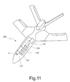
- Figure 11 shows an aircraft 200 comprising the system for automated management of the power 1 or 100 (for managing power supply of one or more primary loads and of one or more secondary loads).
- the system for automated management of the power 1 or 100 makes possible a management of the total load at a local level (i.e., for each single load), unlike traditional management that is made at a central level (that is, pre-arrangement of a plurality of dedicated supply generators is required).
- the present invention enables temporary transfer of power from loads that are not essential to primary loads, which are essential owing to the functions that they perform, in a dynamic way. According to the present invention, it is no longer necessary to size the generators in such a way that they are able to withstand for more or less long periods of time any possible over-supply of current with respect to the nominal value (for example, overloads of 150% for 5 min. or of 200% for 5 s, as aeronautical standards envisage).
- the system according to the present invention presents the advantage of being programmable in its operation, enabling a considerable flexibility in use.
- the behaviour of the management system 1 or 100 can be updated via software (basically updating the current setpoint value I SETPOINT ) not requiring hardware replacement of any component, as would be, instead, necessary in traditional systems of a known type.
- the PID controller (52) can be replaced by a controller configured for carrying out just the proportional action.
- a proportional controller is able to stabilize unstable processes; however, it is not possible to guarantee that the error signal e(t) converges to zero.
- controller configured for carrying out just the proportional and integral actions (proportional-integral, or PI, controller).
- a PI controller has a memory of the past values of the error signal e(t); in particular, the value of the integral action is not necessarily zero if the error signal is zero. This property gives to the PI controller the capacity of bringing the process exactly to the required setpoint, where the proportional action alone would be zero.
- the integral part in time adds up the errors one at a time; this over the long term restores the output variable to the desired values of the setpoint signal. However, this does not prevent an oscillation once the desired value has been reached.
- the derivative action compensates the oscillations without waiting for the error to become significant (proportional action) or for it to persist for a certain time (integral action).
- the derivative action can be omitted in the case where an excessively sensitive controller is not desired.
- a PID controller with derivative action could undergo, for example, a sharp variation at the moment when the setpoint were to be changed practically instantaneously from one value to another, resulting in a derivative of e(t) of a very high value (ideally tending to infinity).
- the integrated chipboard 4 it is possible to configure the integrated chipboard 4 in such a way as to implement other control and stabilization algorithms of a dynamic system, for example control algorithms based upon the theory of optimal control and robust control, known in the literature.
- the management system 1 can be used in other sectors of the art, in particular whenever it is necessary to manage electric power supplies of a plurality of electrical loads in a selective way where particular requirements of reduction of encumbrance and weight are to be respected.
Landscapes
- Engineering & Computer Science (AREA)
- Power Engineering (AREA)
- Remote Monitoring And Control Of Power-Distribution Networks (AREA)
- Dc-Dc Converters (AREA)
Abstract
An electric-power-supply system (1) for supply of a primary electrical load (5) and of a secondary electrical load (3), comprising: a power-supply line (10), configured to carry a main power-supply signal (WTOT), the primary electrical load and the secondary electrical load being connected to the power-supply line; a controlled switch (2, 12) connected between the power-supply line and the secondary electrical load, having a control terminal (12c) receiving a control square-wave signal (VCTR) configured to open and close the controlled switch and having a duty cycle; a current sensor (8), connected to the power-supply line, generating an intermediate current signal (IG) correlated to the main power-supply signal; a microcontroller (50), which receives the intermediate current signal and is configured for: a) generating a mean value of the intermediate current signal (IG); b) detecting whether the mean value of the intermediate current signal is higher or lower than a threshold; c) if it is higher, reducing the duty cycle of the control signal; if it is lower, increasing the duty cycle of the control signal, so as to decrease or, respectively, increase the value of the electric power absorbed by the secondary electrical load (3).
Description
- The present invention relates to a system and a method for automated management of electric power supply, in particular for aeronautical applications.
- The general development of aeronautical technology has led to the design and development of increasingly complex aircraft. This fact has determined widening of the domain of use of electrical energy on board said aircraft.
- The utilizers electrically supplied by the electrical wiring system of the aircraft are various, and may comprise some or all, for example, of the following: lighting system, on-board instrumentation, means for starting the engines, heating and air-conditioning system, fuel pumps, radars, means for driving hydraulic systems, pressurization systems, means for control of operation of the engines, generic command and control devices (relays, contactors, servo-valves, etc.), actuators, and others still.
- In addition to specifically electrical and electronic utilizers and components, which do not allow alternative power supply, there are other that could be supplied differently. For example, various types of actuators can be actuated electrically or via hydraulic and pneumatic circuits, the heating and air-conditioning system can, alternatively, be connected to the pneumatic system (for producing hot and compressed air), and generic command and control devices (relays, etc.) can be implemented by means of fluidic logic elements.
- On board aeroplanes direct-current (DC) electrical energy and alternating-current (AC) electrical energy are typically used. For example, the lighting and heating systems can operate both with DC and with AC, likewise, the engines, can be supplied both with DC and with AC, the command and control devices (relays, warning lights, indicators) generally operate with DC, and the avionics (electronic equipment installed on board the aircraft and having a piloting function) usually operates with AC at 400 Hz, but instruments configured to operate with DC are also provided. Each of these elements of the aircraft absorbs a different percentage of electrical energy for its operation. Typically, the lighting and heating systems use between 50% and 70% of the electrical available energy, the engines between 10% and 40%, the commands and the control devices between 5% and 10%, and the avionics between 5% and 20%.
- The adoption of DC power supply is typical of the components that are most important for survival of the aircraft, which can thus operate even in conditions of emergency, with a battery supply.
- Some systems of the aircraft operate continuously, from takeoff to landing (for example, the avionics), whereas others are activated upon request (for example, the system for actuation of the undercarriage, or the heating system).
- Since different systems require different power supplies with different timings, each aircraft comprises a plurality of generators configured so as to supply the power necessary for the various electrical systems when necessary and facing any possible consumption peaks. Each generator is hence sized appropriately to meet the needs of the system that it supplies.
- The presence of a plurality of generators, however, leads to numerous disadvantages above all in terms of high costs and weight.
- The aim of the present invention is to provide a system and a method for electric power supply, in particular for automated management of electric power supply for aeronautical applications, that will be able to overcome the drawbacks of the known art.
- According to the present invention, a system and a method for electric power supply are provided, as defined in the annexed claims.
- For a better understanding of the present invention, preferred embodiments thereof are now described, purely by way of nonlimiting example and with reference to the attached drawings, wherein:
-
Figure 1 shows a system for management of the supply of electrical energy to a primary electrical load and to a secondary electrical load, wherein the secondary electrical load is connected to a power-supply line via a power-supply device comprising a controlled switch, according to one embodiment of the present invention; -
Figure 2a shows in greater detail a portion of the management system ofFigure 1 , in which the controlled switch is a transistor, according to one embodiment of the present invention; -
Figure 2b shows the power-supply device ofFigure 1 , in which the controlled switch comprises a plurality of transistors connected in parallel to one another, according to a further embodiment of the present invention; -
Figure 3 shows the power-supply device ofFigure 1 according to another embodiment of the present invention; -
Figure 4 shows the management system ofFigure 1 coupled to a heat dissipator; -
Figure 5 shows, by means of a block diagram and according to one embodiment of the present invention, a system for operating the controlled switch ofFigure 2a orFigure 2b ; -
Figure 6 shows, by means of a flowchart, steps of a method implemented by the system ofFigure 5 ; -
Figure 7a shows, by way of example, a signal for operating the controlled switch, generated by the system ofFigure 5 ; -
Figures 7b and 7c show, respectively, mean values of voltage and electric current supplied to the secondary electrical load through the controlled switch, when the latter is operated with the signal ofFigure 7a ; -
Figure 8a shows, by way of example, a further signal for operating the controlled switch, generated by the system ofFigure 5 ; -
Figures 8b and 8c show, respectively, mean values of voltage and electric current supplied to the secondary electrical load through the controlled switch when the latter is operated with the signal ofFigure 8a ; -
Figure 9a shows, by way of example, a further signal for operating the controlled switch, generated by the system ofFigure 5 ; -
Figures 9b and 9c show, respectively, mean values of voltage and current supplied to the secondary electrical load through the controlled switch when the latter is operated with the signal ofFigure 9a ; -
Figure 10 shows the management system according to a further embodiment, configured to supply electrical energy to a plurality of primary and secondary electrical loads; and -
Figure 11 shows an aircraft comprising the management system ofFigure 11 . - According to the present invention, management of the electrical energy that is to be supplied to a plurality of electrical loads of an aircraft occurs in a local and centralized way. There is thus no need to have available a plurality of generators, as many as are the electrical loads to be supplied. In particular, management of the overloads occurs by managing the energy supplied to each load in such a way as to reduce the supply of the energy to loads that are non-operative or non-essential for survival of the aircraft, for supplying appropriately and preferentially the electrical loads fundamental for survival of the aircraft.
-
Figure 1 is a schematic illustration of amanagement system 1 for automated management of the electrical energy (or electric power) to be supplied to a primaryelectrical load 5 and to a secondaryelectrical load 3. - The primary
electrical load 5 is directly connected to a power-supply line 10, whereas the secondaryelectrical load 3 is supplied via a power-supply device 2 set to form an interface between the power-supply line 10 and the secondaryelectrical load 3. The primaryelectrical load 5 is a load, operation of which is of particular importance for the system in which it operates and which must be supplied with priority with respect to the secondaryelectrical load 3. For this reason, the primaryelectrical load 5 is directly supplied by the power-supply line 10, whereas the power supply of the secondaryelectrical load 3 is entrusted to the power-supply device 2 (operation of which will be described hereinafter). With reference to an aircraft, the primaryelectrical load 5 comprises, for example, the engines of the aircraft and/or the avionics, whereas the secondary electrical load comprises, for example, the system for lighting the cabin or the heating system. - During use, the primary
electrical load 5 absorbs a part of the voltage or power with respect to the total amount available on the power-supply line 10. The voltage or power remaining on the power-supply line 10 is used (either totally or in part) by the secondaryelectrical load 3. - The
management system 1 comprises: the power-supply device 2, configured for regulating the power supplied to the secondaryelectrical load 3, which receives an input supply signal VDC_IN in direct current (DC) for example at 270 V, and which supplies at output an output power-supply signal VDC_OUT, which is also in direct current; an integratedchipboard 4, for example comprising a microcontroller, for controlling the operations of the power-supply device 2 so as to manage appropriately the energy supplied by the power-supply device 2 to the secondaryelectrical load 3; alevel amplifier 6, connected between the integratedchipboard 4 and the power-supply device 2, configured for on-state and off-state driving of the power-supply device 2 on the basis of a control signal, for example a PWM (pulse width modulated) signal, generated by the integratedchipboard 4; and acurrent sensor 8. - The power-supply signal that flows on the power-
supply line 10 is generated by a power-supply generator 11, for example a voltage generator. Thecurrent sensor 8 is connected between thegenerator 11 and the power-supply line 10, for detecting the current effectively supplied by the power-supply generator 11 during use. - The integrated
chipboard 4 is, for example, based upon an Arduino hardware platform. - The power-
supply line 10 is an electrical line that carries a DC power-supply signal (which can be identified on the basis of the voltage VTOT, for example 270 VDC, of the current ITOT, for example 100 A for voltages of 270 V, and/or of the power WTOT=VTOT·ITOT) for supplying generic electrical apparatuses (loads) of the aircraft. - The power-
supply line 10 is the typical DC power-supply line present on all aircraft (the so-called "aeroplane DC busbar"). The input signal VDC_IN of the power-supply device 2 is taken from the power-supply line 10. - The
current sensor 8 transduces the current that flows on the power-supply line 10 into a voltage signal (for example, comprised between approximately 0 V and 5 V) proportional to the current that flows on the power-supply line 10. The signal generated at output by the current sensor is a signal indicating the current that flows, at the instant of measurement, on the power-supply line 10 (upstream of any electrical load), and varies linearly as said current varies. According to one embodiment of the present invention, the integratedchipboard 4 operates on digital signals. The voltage signal generated at output by thecurrent sensor 8 is consequently converted into a digital signal by means of an analog-to-digital converter (not shown), for example operating on 8 bits, and assumes a value comprised between 0 and 255. The numeric value (0-255) assumed by the voltage signal generated at output by thecurrent sensor 8 consequently indicates the voltage value (0-5 V) of the signal generated by thecurrent sensor 8, which, in turn, indicates the current value (0-100 A) measured on the power-supply line 10. In the final analysis, hence, thedigital value 0 is associated to the current value 0 A, and thedigital value 255 is associated to thecurrent value 100 A. It is moreover possible to associate to the digital value 255 a higher current value, for example 150 A or 200 A or higher so as to be able to represent on 8 bits any possible over-supplies of current with respect to the nominal value. The aforementioned current values regard an example according to one embodiment, and in no way limit the scope of the present invention. - The power-
supply device 2 comprises a controlled switch 12 (for example, formed by a single MOSFET or by a plurality of MOSFETs connected in parallel to one another), which has a first conduction terminal connected to the power-supply line 10, a second conduction terminal connected to the secondaryelectrical load 3, and a control terminal configured to receive a control voltage signal that assumes alternatively a first value such as to close the controlled switch 12 (which in this state conducts electric current) and a second value such as to open the controlled switch 12 (which in this state does not conduct electric current). The control signal of the controlledswitch 12 is hence a signal having a square waveform, with a certain duty cycle. The duty cycle can be varied during use so as to set appropriately the duration of the intervals in which the controlledswitch 12 conducts current with respect to the duration of the intervals in which the controlledswitch 12 does not conduct current. - When the controlled
switch 12 is closed, the secondaryelectrical load 3 is coupled to the power-supply line 10 (thus absorbing current), whereas when the controlledswitch 12 is open the secondaryelectrical load 3 is decoupled from the power-supply line 10 (and does not absorb current). - By varying the duty cycle which controls the controlled
switch 12, the mean power supplied, in a certain time interval, to the corresponding secondaryelectrical load 3, is varied consequently. It is thus possible to set, according to the need, the value of power that it is desired to supply to the secondaryelectrical load 3, in a dynamic way. - The duty cycle of a control signal is given by the ratio between the duration of the control signal at a high level and the total period of the control signal, and expresses for what portion of period the control signal is at a high level (where by "high" is meant the active level of the signal). In the case discussed here, by "high" or "active" level is meant the level that is able to close the controlled switch 12 (i.e., during which the controlled
switch 12 conducts electric current), irrespective of the type of controlledswitch 12 used. - The signal generated at output by the
current sensor 8 is correlated (proportional) to the power-supply signal of the power-supply line 10 (VTOT and/or ITOT and/or WTOT). In particular, the signal generated at output by, thecurrent sensor 8 is correlated (proportional) to the current ITOT that flows in the power-supply line 10. - The
integrated chipboard 4 receives at input the signal generated at output by thecurrent sensor 8, and carries out the following operations: a) it computes a mean value of the signal generated at output by thecurrent sensor 8, averaged over a certain time interval or over a number of predefined samples of the signal generated at output by the current sensor 8 (in this latter case, the signal generated by thecurrent sensor 8 is first sampled by means of an analog-to-digital converter); b) it detects a deviation of the mean value computed in point a) with respect to a threshold (said threshold is set to the maximum current value that the power-supply line can withstand for operating in safety conditions); and c) in the presence of the deviation referred to in point b), it varies the duty cycle of the control signal of the power-supply device 2 until the mean value of the signal generated by thecurrent sensor 8 assumes a value approximately equal to the threshold value. The variation of the duty cycle, in fact, causes the value of the electric power absorbed by the secondary electrical load 3 (or, from another standpoint, the value of the electric power that the power-supply device 2 supplies to the secondary electrical load 3) to vary. - The deviation referred to in the aforementioned point b) can regard a mean value of the signal generated at output by the
current sensor 8 higher than the threshold, or a mean value of the signal generated at output by thecurrent sensor 8 lower than the threshold. - The operation of reduction of the duty cycle of the control signal causes a lower consumption of electrical energy by the secondary electrical load 3 (it increases the time in which the controlled
switch 12 is off in proportion to the time in which the controlledswitch 12 is on). Consequently, on the power-supply line 10 there is an increase of the energy available that can be used by the primaryelectrical load 5; the primaryelectrical load 5 can thus be supplied with the power that it requires, reducing the likelihood of incurring in risks of overvoltages or overcurrents on the power-supply line 10. In the absence of said regulation, a request for oversupply by the primaryelectrical load 5 would be managed exclusively by thegenerator 11, which could find itself working in limit conditions, supplying more power than what is envisaged for an operation in safety conditions for itself and for the power-supply line 10. - In limit conditions, the secondary
electrical load 3 might not be sufficiently supplied, but operation of the primaryelectrical load 5 is in all cases guaranteed. -
Figure 2a is a schematic illustration of the power-supply device 2 comprising the controlled switch 12 (in particular, a MOSFET of an N type) having afirst conduction terminal 12a (in particular, a drain terminal) connected to the power-supply line 10, asecond conduction terminal 12b (in particular a source terminal) connected to the secondaryelectrical load 3, and acontrol terminal 12c (in particular a gate terminal) connected to the output of thelevel amplifier 6. In this way, the gate terminal is controlled by thelevel amplifier 6 with voltages that have a dynamics such as not to damage the MOSFET. It is evident that, by configuring theintegrated chipboard 4 for driving the MOSFET in opening/closing using adequate voltages, such as not to damage the MOSFET, thelevel amplifier 6 is not necessary. - To withstand high current/voltage values,
Figure 2b shows a further embodiment of the power-supply device 2, comprising a plurality oftransistors 12, in particular N-channel MOSFETs, which have respectivefirst conduction terminals 12a (drain terminals) connected to one another and to the power-supply line 10, respectivesecond conduction terminals 12b (source terminals) connected to one another and to the secondaryelectrical load 3, andrespective control terminals 12c (gate terminals) connected to one another and to the output of thelevel amplifier 6. - The number and type of MOSFETs is chosen according to the need on the basis of the voltages/currents to be withstood in the specific application of the power-
supply device 2. The operations of opening (inhibition) and closing (conduction) occur consequently in a synchronous way for all the MOSFETs of the power-supply device 2 ofFigure 2b . The power-supply device 2 ofFigure 2b operates, from a conceptual standpoint, as a single MOSFET (having a first conduction terminal and a second conduction terminal and a control terminal). In what follows, reference will consequently be made to a "controlledswitch 12" or "power-supply device 2" without limitation to a particular embodiment from among the ones shown inFigures 2a andFigure 2b . - It is moreover evident that the power-
supply device 2 may comprise transistors or generic controlled switches of a type different from an N-type MOSFET, for example a P-type MOSFETs, a JFETs, a MESFETs, bipolar transistors, or others still. - In use, as illustrated more clearly in what follows, the controlled
switch 12 is controlled alternatively in opening (inhibition), and closing (conduction) by means of the control signal VCTR, if necessary conditioned by thelevel amplifier 6, and applied to thecontrol terminal 12c. The control signal VCTR is, in particular, a voltage signal having a maximum value of some volts (for example, 10 V), configured to drive the controlledswitch 12 in opening and closing (the control signal VCTR is, as mentioned previously, a square-wave signal). If the controlledswitch 12 is an N-channel MOSFET, when the value of the control signal VCTR exceeds a minimum threshold (i.e., it has a first value), thegate terminal 12c is biased in such a way as to generate a conductive channel between thesource terminal 12b and thedrain terminal 12a so as to connect the power-supply line 10 to the secondaryelectrical load 3 and hence supply the secondaryelectrical load 3; instead, when the value of the control signal VCTR is lower than a minimum threshold (i.e., it has a second value), the controlledswitch 12 is inhibited to uncouple the power-supply line 10 from the secondaryelectrical load 3. - With particular reference to the avionics application, the controlled
switch 12, irrespective of the embodiment of the latter, is configured to operate preferably at a maximum working voltage of 285 VDC, and is configured to withstand a maximum working current of approximately 100 A at 270 VDC. Other applications may require different voltage and current values, either higher or lower. -
Figure 3 shows, according to one embodiment of the present invention, the power-supply device 2 comprising, in addition to the controlledswitch 12, a plurality of further electrical and electronic elements. - The input supply signal VDC_IN is applied at input to the power-
supply device 2 between afirst input pin 7a and asecond input pin 7b, respectively at the voltage V+ DC_IN and V- DC_IN, where thefirst input pin 7a is connected to the drain terminal of the MOSFET that forms the controlled switch 12 (as has been said, other types of transistors or controlled switches can be used). - The output power-supply signal VDC_OUT is supplied at output between a
first output pin 9a and asecond output pin 9b, respectively at the voltage V+ DC_OUT and V- DC_OUT, where thefirst output pin 9a is connected to the source terminal of the MOSFET that in this example forms the controlledswitch 12. - The power-
supply device 2 comprises an opto-insulation board 13, configured to form an interface between thelevel amplifier 6 and thecontrol terminal 12c of the controlledswitch 12. In this way, any possible disturbance (voltage/current peaks) carried by the control signal VCTR do not damage the controlledswitch 12. The working principle of the opto-insulation board is known. Typically, an opto-insulation board (or, simply, optoinsulator) comprises a LED, set at an input of the optoinsulator, configured to receive the control signal VCTR (or, alternatively, a current signal that is a function of the control signal VCTR) and generate at output a light signal that is a function of the control signal VCTR. The light signal thus generated is supplied at input to a photodiode, which generates on one of its outputs an electrical signal VC_OPT that is a function of the light signal generated by the LED. In the final analysis, hence, the electrical signal VC_OPT generated by the photodiode is correlated to (or is a function of) the control signal VCTR. - The signal at input to the LED may, if necessary, be reduced in intensity using a resistor set upstream of the LED. By introducing a resistor having low resistance (or not introducing the resistor), the LED is biased with a voltage/current having a high value, to obtain a light signal generated by the LED having high intensity. In this case, the variation in intensity of the light signal due to the variations of the voltage/current signal at input to the LED is far from readily perceptible, a fact that is positive from the standpoint of rejection of the disturbance at input. Instead, with a resistor having high resistance, the light signal generated by the LED is more correlated to the variations of voltage/current of the signal at input to the LED.
- As regards, instead, the photodiode, it is typically reversely biased. It is evident that the signal generated at output by the photodiode will replicate more or less faithfully the variations of the control signal VCTR, the more the light signal generated by the LED replicates faithfully said variations. For the embodiment considered according to the present invention, it is advisable to use optoinsulators in which spurious variations of the control signal VCTR are not replicated, or are minimally replicated, on the light signal generated by the LED (this is obtained, as has been said, using at input to the LED resistors that have a low value of resistance). In fact, as has been said, the control signal VCTR is a square-wave signal having two states: a high state, or ON state, where the control signal VCTR has a maximum value, and a low state, or OFF state, where the control signal VCTR has a minimum value.
- The power-
supply device 2 further comprises aSchmitt trigger 14, connected on an output of the opto-insulation board 13, which receives at input the electrical signal VC_OPT generated as illustrated previously, and is configured to square the electrical signal VC_OPT to obtain a squared signal VC_TRIG having steeper rising and falling edges typical of the digital signal. The squared signal VC_TRIG biases thecontrol terminal 12c of the controlledswitch 12, controlling opening thereof (inhibition state) and closing thereof (conduction state). - The squared signal VC_TRIG is correlated to the electrical signal VC_OPT, and hence correlated to the control signal VCTR, and replicates it faithfully. The squared signal VC_TRIG, in particular, has the same duty cycle as the control signal VCTR, and is delayed with respect to the control signal VCTR on account of the operations carried out by the opto-insulation board. Said delay consequently depends upon the opto-insulation board used, and it is preferable for it to have a time duration that is as short as possible.
- The power-
supply device 2 further comprises athermostat 16, set in the proximity of the controlledswitch 12, for monitoring the temperature reached by the latter during use. Thethermostat 16 can be set in the proximity (for example, at a distance of a few millimetres) of apackage 18 that houses the controlledswitch 12, or else in direct contact with thepackage 18. Alternatively, thethermostat 16 can be set inside thepackage 18. - The power-
supply device 2 further comprises acurrent shunt 22, also known simply as "shunt", configured to supply a measurement of the current that flows through the controlledswitch 12. Thecurrent shunt 22 basically comprises a shunt resistor (not shown) configured to shunt through itself a part of the current that flows through the controlledswitch 12. As is known, the shunt resistor is connected in parallel to the line on which the current that is to be measured flows (downstream of the controlled switch 12). Operation of a current shunt is well known in the art, and is not further described herein, for brevity. - As an alternative to the
current shunt 22, it is possible to use any other device configured to measure the value of current that flows through the controlledswitch 12. - The
current shunt 22 generates at output a measurement signal VM (voltage signal) proportional to the current that flows in the controlledswitch 12. The power-supply device 2 further comprises afeedback circuit 26, which receives at input the measurement signal VM generated at output by the current shunt 22 (voltage signal, proportional to the current that flows in the controlled switch 12) and carries out on said measurement signal VM an operation of conditioning for limiting the dynamics thereof within a predefined interval, for example comprised between approximately 0 and 10 V, generating a feedback signal VFB (voltage signal). The feedback signal VFB is then sent at input to the opto-insulation board 13. Operation of thefeedback circuit 26 is useful for adapting the measurement signal VM to the input dynamics of the opto-insulation board 13. - The power-
supply device 2 further comprises adiode 27 connected between thesecond input pin 7b (V- DC_IN) and thefirst output pin 9a (V+ DC_OUT). Thediode 27 has the function of preventing damage of thecomponent 12 when the load has an inductive component. Thediode 27 is configured for withstanding a maximum voltage between the anode and the cathode of 400 V, a DC forward current, at an operating temperature of 104°C, of a maximum value of 150 A, and a single-pulse forward current, at an operating temperature of 25°C, of a maximum value of 1500 A. The operating temperatures are comprised between -55°C and 175°C. Diodes of this type are known and readily available on the market. - Connected in parallel to the
diode 27 is afilter 28, comprising aresistor 28a connected in series to acapacitor 28b (RC network). Thefilter 28 has the function of reducing current/voltage peaks that may occur during switching of the signal VCTR (which, as has been said, is of the square-wave type, for example of the PWM type). The RC network, in fact, opposes the sharp variations of voltage, absorbing current and consequently causing a considerable reduction in the voltage variations. - The power-
supply device 2 further comprises analarm circuit 30, comprising amicroprocessor 31 configured for generating alarm signals in critical situations of operation of the power-supply device 2, and/or in the case of any malfunctioning of the power-supply device 2. - The
alarm circuit 30 receives at input a temperature alarm signal ST generated by thethermostat 16. In particular, the temperature alarm signal ST is generated by thethermostat 16 when the operating temperature of the controlledswitch 12 detected by thethermostat 16 exceeds a certain maximum threshold. Said threshold is, for example, equal to 100°C. - According to a further embodiment, the
thermostat 16 generates a plurality of temperature alarm signals, each corresponding to a different threshold with a different criticality. For example, thethermostat 16 generates: a first temperature alarm signal ST' when the temperature of the controlledswitch 12 reaches a low-criticality level, for example equal to 90°C; a second temperature alarm signal ST" when the temperature of the controlledswitch 12 reaches a medium-criticality level, for example, equal to 100°C; and a third temperature alarm signal ST"' when the temperature of the controlledswitch 12 reaches a high-criticality level, for example, equal to 150°C. - According to an alternative embodiment, the
thermostat 16 generates at output a temperature alarm signal ST either continuously or at regular time intervals, where said temperature alarm signal ST indicates the instantaneous operating temperature of the controlledswitch 12. The verification of possible criticalities (comparison with one or more thresholds, in a way similar to what has been described previously) is carried out, in this case, directly by thealarm circuit 30. - The
alarm circuit 30 moreover receives the feedback signal VFB generated by thefeedback circuit 26. Themicroprocessor 31 is hence moreover configured for processing the feedback signal VFB in order to detect whether the current that flows in the controlledswitch 12 reaches excessively high values (for example, on account of malfunctioning of the logic-state device 12). Said detection is made, for example, by comparing the value of the feedback signal VFB with a predefined threshold. - The
alarm circuit 30 moreover supplies to the opto-insulation board 13 a plurality of integrity signals SMOSFET_KO, SMOSFET_DC, SOVP, SOT configured to supply information on the integrity and operation of the controlledswitch 12. - For its own part, the opto-
insulation board 13 receives the integrity signals SMOSFET_KO, SMOSFET_DC, SOVP, SOT and supplies them at output from the power-supply device 2 for being processed and managed appropriately (the further management of the alarm signals does not form the subject of the present invention, and hence the corresponding procedures are not described any further). The opto-insulation board 13 hence operates as only input/output interface for the control signals (VCTR; VC_TRIG) and management signals (the integrity signals SMOSFET_KO, SMOSFET_DC, SOVP, SOT) of the power-supply device 2. - The integrity signal SOT is an alarm signal indicating an operating overtemperature of the solid-
state device 12. The integrity signal SOT is hence associated to the temperature alarm signal ST generated by thethermostat 16 and received by thealarm circuit 30 and can assume all the meanings of criticality described previously with reference to the temperature alarm signal ST for the various embodiments. - The integrity signal SOVP is an alarm signal indicating an overvoltage of the input supply signal VDC_IN. In order to monitor the input voltage, the
alarm circuit 30 has an input coupled to thefirst input pin 7a (V+ DC_IN). The input supply voltage thus received via thefirst input pin 7a is normalized within a predefined range of values, such as to be managed by themicrocontroller 31, and then constantly compared with a predefined threshold, chosen on the basis of the characteristics of the controlled switch 12 (for example, equal to the maximum voltage that the controlledswitch 12 is able to withstand). If the voltage of the input supply signal VDC_IN remains above the predefined threshold beyond a certain time, said critical situation is signalled by means of the integrity signal SOVP. The consequences of such a critical situation do not form the subject of the present patent application and hence are not further described herein. By way of example, in any case, in order to overcome said situation the control signal VCTR could be forced to a value such that the solid-state device is driven into an open condition, uncoupling the power-supply line 10 from the secondaryelectrical load 3. - The integrity signal SMOSFET_DC is an alarm signal indicating the state of conduction of the controlled
switch 12, generated on the basis of the feedback signal VFB, and hence proportional to the current that flows through the controlledswitch 12. Any possible variations of the current that flows through the controlled switch 12 (measured as described previously) with respect to the expected condition during supply of the secondaryelectrical load 3 may be indicative a malfunctioning of the controlledswitch 12. - The integrity signal SMOSFET_KO is an alarm signal indicating the state of the line that supplies the secondary
electrical load 3, and is generated on the basis of the voltage signals picked up on thefirst output pin 9a and on thesecond input pin 7b and processed (after prior appropriate conditioning) by themicrocontroller 31. Any possible alterations of said signals with respect to the expected signal are indicative of possible malfunctioning of the power-supply line of the secondaryelectrical load 3. - Some or all from among the opto-
insulation board 13, theSchmitt trigger 14, thecurrent shunt 22, thefeedback circuit 26, and thealarm circuit 30 that were, for their operation, to require an external power supply, further comprise a power-supply input of their own, configured to receive a power-supply signal VCC having an appropriate voltage value according to their own supply characteristics (inFigure 3 just the opto-insulation board is shown, by way of example, connected to an external power supply VCC). -
Figure 4 shows, in perspective view, apackage 40 within which the power-supply device 2 is housed (the latter being arranged on an integrated chipboard 41). - In order to reduce to a minimum the problems regarding overheating of the power-
supply device 2,Figure 4 shows aheat dissipator 42, set in contact with an outer surface of thepackage 40, for cooling the latter during operation. The ideal operating temperature of the controlledswitch 12 is approximately 85°C. Theheat dissipator 42 is consequently configured to cool the region inside thepackage 40 so as to maintain the optimal operating temperature, or in any case a temperature comprised between approximately 70°C and 95°C. Further means for cooling the controlledswitch 12 can be envisaged, for example one or more fans (not shown) set inside thepackage 40, in the proximity of the controlledswitch 12. - The
heat dissipator 42 is, according to one embodiment of the present invention, of a liquid-cooled type, and comprises aninlet channel 42a through which a cooling liquid enters theheat dissipator 42, and anoutlet channel 42b through which the cooling liquid exits from theheat dissipator 42. The cooling liquid is, for example, water having a temperature equal to or lower than 18°C, which flows at a rate of approximately 8 1 per min. Said values have proven sufficient to guarantee the aforementioned levels of performance considering a thermal power to be dissipated P = 300W, a desired temperature inside the package 40 (for example, made of thermally conductive material to favour heat dissipation) of approximately 85°C, and an area of heat exchange between thepackage 40 and theheat dissipator 42 of approximately 0.0228 m2. The present applicant has verified that, in the aforementioned conditions, theheat dissipator 42 is able to maintain a temperature range in thepackage 40 of 70°C with powers to be dissipated P=600W. This oversizing of theheat dissipator 42 guarantees good levels of performance even in unforeseen critical conditions. - According to one embodiment, the
heat dissipator 42 has inside a cavity, brazed in which are a series of fins, made of corrugated aluminium. The fins create a turbulence of the cooling liquid that minimizes the limit layer and reduces the thermal resistance, thus obtaining a high global heat-exchange coefficient. - With reference to
Figure 5 , there now follows a description of a system and a method for driving the power-supply device 2, and in particular for driving the controlled switch 12 (generation of the control signal VCTR). -
Figure 5 shows acontrol circuit 50, according to one embodiment of the present invention. - The
control circuit 50 comprises acontroller 52 of the proportional-integral-derivative (PID) type. ThePID controller 52 comprises anadder 52a, configured to receive a reference, or "setpoint", signal ISETPOINT, and a signal that is to be compared with the setpoint signal ISETPOINT (feedback signal IR, described more fully hereinafter). - The setpoint signal ISETPOINT identifies the maximum current that can flow on the power-
supply line 10 for operating in a safety condition (i.e., without the risk of damaging the power-supply line 10 itself and/or the generator 11). The setpoint signal ISETPOINT can have a predetermined fixed value, stored in anon-rewritable memory 53, or else a value that can be updated according to the need (in this latter case, thememory 53 is of a rewritable type and comprises an access port for writing). - The setpoint signal ISETPOINT is, for example, a numeric value represented on 8 bits, and can assume a value comprised between 0 and 255, where 0 is associated to a current of 0 A, and 255 is associated to the maximum current envisaged (linear association). It is moreover possible to associate to the maximum current envisaged a numeric value lower than 255 to guarantee a certain safety margin.
- The
adder 52a is configured to generate at output a difference signal ID given by the difference between the setpoint signal ISETPOINT and the feedback signal IR (ID=ISETPOINT-IR). Consequently, operating in the digital domain, the difference ISETPOINT-IR is made between numeric signals on 8 bits indicating respective current values. In this way, there is ensured consistency between all the values on which the operations are performed. - The feedback signal IR is obtained as time average of the current signal IG, which is correlated to the current value ITOT present on the power-
supply line 10. The current signal IG is the signal generated at output by thecurrent sensor 8 shown inFigure 1 , and indicates the current value measured on the power-supply line 10 by thecurrent sensor 8. - If the current value on the power-supply line 10 (averaged value IR), and the desired value of current on the power-supply line 10 (given by the setpoint value ISETPOINT) are known, the
PID controller 52 is able to react to a possible positive or negative error of the value of IR with respect to the desired value ISETPOINT to bring the difference signal ID to the value 0 (i.e., IR=ISETPOINT). - The
PID controller 52 is typically implemented by means of a software program. The signals ISETPOINT, IR, IG, ID shown inFigure 5 are, in this case, digital signals. The setpoint signal ISETPOINT is pre-set at a value equal to the maximum current that can be supplied on the power-supply line 10 by the power-supply generator 11, the signal IG is a signal that identifies instant by instant the current value ITOT that flows on the power-supply line 10, and the feedback signal IR is a signal obtained as average of a plurality of values assumed by the signal IG. Theadder 52a generates at output an error signal (ID) indicating the difference between the desired signal (setpoint signal ISETPOINT) and the signal effectively present on the power-supply line 10. Operation of theadder 52a (ID=ISETPOINT-IR) is hence carried out on the basis of a current value on the power-supply line 10 that is stable (averaged over a certain time and/or a certain number of samples) and not instantaneous (an instantaneous value is subject to unforeseable fluctuations). The error signal ID can have a negative value (on the power-supply line 10 there flows more current than the one envisaged as the maximum possible one for use in safety conditions) or a positive value (on the power-supply line 10 there flows less current than the one envisaged as the maximum possible one for use in safety conditions). - The
PID controller 52 further comprises anoperating block 52b, having the known transfer function D(s) typical of PID controllers of a known type
- The values of the parameters Kp, Ki, and Kd depend upon the load of the
PID controller 52, and are set as a function of said load. A known method for setting said parameters is referred to in the literature as the "Ziegler-Nichols rules". Another method known in the literature is, for example, the "Cohen and Coon method". - In particular, the transfer function of the
PID controller 52 is chosen in such a way that the time of reaction of the system (time for reaching the setpoint) is shorter than 50 ms, the stabilization time (time for reduction of the error within 5%) is shorter than 2 s, and the maximum overshoot is lower by 5% than the setpoint value. - The Ziegler-Nichols method is known, and basically comprises the following steps: the process is controlled by an exclusively proportional controller (Ki, and Kd are set to zero); the gain Kp of the proportional controller is gradually increased; the critical gain Ku is the value of the gain such that the controlled variable presents sustained oscillations, i.e., ones that do not disappear after a transient: this is a measurement of the effect of the delays and of the dynamics of the process; the critical period Pu of the sustained oscillations is recorded; the constants Kp, Ki, and Kd are determined as Kp=0.6·Ku, Ki=Pu/2, and Kd=Pu/8.
- For example, for a load of some hundred watts, the optimal values of Kp, Ki, Kd are respectively 0.5, 1000, and 0.001.
- The output from the
PID controller 52 is a signal SPID that is used by aPWM modulator 54 for generating a square-wave voltage signal VPWM. It is here assumed that the input of the PWM modulator accepts a signal on 8 bits, with values comprised between 0 and 255. Hence, the signal SPID is a digital signal on 8 bits that assumes values comprised between 0 and 255, where SPID=O is interpreted by thePWM modulator 54 as a command for generating a square-wave voltage signal VPWM with duty cycle of 0%, and SPID=255 is interpreted by thePWM modulator 54 as a command for generating a square-wave voltage signal VPWM with a duty cycle of 100%. Intermediate values of duty cycle (between 0 and 100%) are driven by respective intermediate values (between 0 and 255) of the signal SPID, with linear association (in a way proportional to one another). For example, a duty cycle of 80% is determined by a value SPID=204. Internally, thePWM modulator 54 operates in a way in itself known and is hence not described any further herein. - The square-wave voltage signal VPWM is supplied at input to the
level amplifier 6; the latter generates, according to the square-wave voltage signal VPWM, the control signal VCTR (which follows faithfully the square-wave voltage signal VPWM but has maximum and minimum values such as to drive the controlledswitch 12 in opening and closing without damaging it). - According to the embodiment of the power-
supply device 2 ofFigure 3 , the control signal VCTR is supplied at input to the opto-insulation board 13 and not to the controlledswitch 12. In this case, the control signal VCTR has maximum and minimum values such as not to damage the opto-insulation board 13. It is evident that thelevel amplifier 6 might not be necessary in the case where the square-wave voltage signal VPWM has maximum and minimum values such as not to damage the controlledswitch 12 or the opto-insulation board 13 (according to the embodiment chosen for the power-supply device 2); in this case, the square-wave voltage signal VPWM coincides with the control signal VCTR. - The
control circuit 50 further comprises an averagingblock 56, configured for receiving the signal ID and generating the feedback signal IR. - The averaging
block 56 may be, for example, an integrator. The feedback signal IR is generated in this case on the basis of a time average (between the instants tA and tB) of the current signal IG. A typical value of the interval tA-tB is in the region of 4 ms. - The operation performed by the integrator is described by the following analytical formula:

- Alternatively, the averaging
block 56 operates on digital signals ID and IR, and is designed for computing a mean on a predefined number n_s (for example, n_s=30) of samples of the current signal IG. In this case, the current signal IG is first sampled (by means of an analog-to-digital converter, not shown), and then the averaging operation is carried out by the averaging block according to the following formula to obtain the feedback signal IR:
- Hence, in this case, the feedback signal IR is a numeric signal that illustrates the mean current value present on the power-supply line during the time interval to which the samples of IG acquired belong.
- In use, in the case where the feedback signal IR assumes a value higher than the value of the setpoint signal ISETPOINT, the
control circuit 50 generates a square-wave voltage signal VPWM having a duty cycle such as to reduce the energy consumption of the secondary electrical load 3 (seeFigure 1 ). Namely, the value of the duty cycle of the square-wave voltage signal VPWM is progressively reduced until there are guaranteed, simultaneously, power supply of theelectrical load 5 and maintenance, on the power-supply line 10, of a current not higher than the one envisaged, identified, as has been said, by of the setpoint signal ISETPOINT. This is obviously at the expense of supply of the secondaryelectrical load 3, which will see a progressive reduction of the power supplied to it. - If, instead, the value of the feedback signal IR is below the value of the setpoint signal ISETPOINT, the duty cycle of the square-wave voltage signal VPWM is increased, guaranteeing an adequate power supply of the secondary
electrical load 3. It is here pointed out that only the secondaryelectrical load 3 is connected to the power-supply line 10 via the power-supply device 2, theelectrical load 5 is directly connected to the power-supply line 10 and consequently is not subject to reductions of supply made by the power-supply device 2. -
Figure 6 shows, by means of a flowchart, the operations performed by thePID controller 52. From a mathematical standpoint, thePID controller 52 is configured for generating the following output:
where e(t) is a time-variable error parameter, given by the deviation of the desired value of current (setpoint value ISETPOINT) with respect to the real value of current that flows on the power-supply line 10 (identified by IR, which, as has been said, is a mean value in a certain time interval of the instantaneous real current values). Hence e(t)=ID=ISETPOINT-IR. - As may be noted from the previous formula, the
PID controller 52 supplies an output having: a proportional term, obtained by multiplying the error signal e(t) by the constant Kp; an integral term, proportional to the time integral of the error signal e(t) multiplied by the constant Ki; and a derivative term. As has been said, operations of a PID controller are well known in the literature, and are given herein for greater clarity. - In the first place (step S1 of
Figure 6 ), the parameters Ki_m=Ki·Δt and Kd_m= Kd/Δt are defined, where Δt is a pre-set interval, for example 0.1 s. The steps ofFigure 6 are not carried out at each instant, but at intervals Δt. Also the mean value assumed in the interval Δt by the current signal IG is computed to obtain, as already illustrated, the feedback signal IR. - Then (step S2), the error parameter ID is computed as ISETPOINT-IR.
- Next (step S3), the integral term ITERM is computed as ITERM=ITERM+Ki_m·ID. In detail, step S3 carries out the operation of integration according to the following approximation

- Then (step S4), a check is made to verify whether the value of ITERM computed in step S3 exceeds the
value 255. If it does (output YES), control passes to step S5, where the value of ITERM is reduced to 255 and then passes to step S8; if it does not (output NO), control passes to step S6. The presence of the step S4 is determined by the fact that it has been assumed that thePWM modulator 54 accepts at input signals on 8 bits. Thevalue 255 can be varied in the case where aPWM modulator 54 is used that is able to accept at input a signal on a greater or smaller number of bits. - In step 56 a check is made to verify whether the value of ITERM computed at step S3 is lower than 0. In it is (output YES), control passes to step S7, where ITERM is set to the
value 0; otherwise (output NO), control passes to step S8. - In step S8, the derivative term Kd·de(t)/dt is computed as

- It is here pointed out that the time derivative of ISETPOINT is zero, since, as has been said, ISETPOINT is chosen with a value constant in time.
- The operation carried out in step S8 is consequently the calculation of dIR as dIR=IR-IR_last, where IR_last is the last value of IR calculated. Since, as illustrated hereinafter, the process of
Figure 6 is iterative, at the first iteration IR_last is initialized at the value zero. - Then (step S9), the output of the
PID controller 52 is computed as:
- Next (step S10), a check is made to verify whether the value of SPID is greater than 255; if it is (output YES), control passes to step S11, where the value of SPID is reduced to 255 (as has already been said, so that it can be represented on 8 bits), and control passes to step S14.
- In the case of output NO from step S10 (the value of SPID is lower than 255), a check is made (step S12) to verify whether the value of SPID is lower than 0; if it is (output YES), control passes to step S13, where the value of SPID is set to 0, and then to step S14. Output NO from step S12 does not alter the value obtained for SPID, and control passes to step S14.
- In step S14 the value of the variable IR_last is updated, for the next iteration, at the current value, i.e., IR_last=IR.
- Control then returns to step S2, and the cycle described is resumed. Between step S14 and step S2 a wait step S15 is envisaged, for waiting for a time Δt (for example, as has been said, of 0.1 s). During step S15 the mean value of the current signal IG in Δt is also updated to obtain a new value of the feedback signal IR.
- At each iteration, the value obtained for SPID is a number comprised between 0 and 255 in binary digits (i.e., represented on 8 bits), and is supplied at input to the
PWM modulator 54. ThePWM 54 generates, on the basis of the value of the signal SPID, as has been said, a square-wave signal VPWM having duty cycle variable between 0% and 100%. The duty cycle of VPWM varies between 0% and 100% in a linear way with the variation of SPID between 0 and 255. - The operations described with reference to steps S1-S14 are typically carried out by means of a software program configured for said purpose. The operations carried out during steps S1-S14 are made on a number of bits higher than 8 bits, and then converted on 8 bits after step S14, prior to input to the
PWM modulator 54. -
Figure 7a shows variations of the control signal VCTR (the rising and falling edges of which correspond to the respective edges of the square-wave signal VPWM) that determines a variation of the supply voltage VDC_OUT (Figure 7b ) and current ISEC (Figure 7c ) of the secondaryelectrical load 3, caused by corresponding variations of the absorption of energy by the primaryelectrical load 5. - With reference to
Figure 7a , between the instant to and the instant t1, it is assumed that the primaryelectrical load 5 is on at its nominal power WL1 and the secondaryelectrical load 3 is at its nominal power WL2. The control signal VCTR, in the interval t0-t1, has a high value "H", and the controlledswitch 12 is closed (i.e., it conducts electric current). It is assumed, for simplicity of description, that WL1+WL2=WTOT (i.e., all the energy WTOT supplied by the power-supply line 10 is used for supply of the secondaryelectrical load 3 and of the primary load 5). - With reference to
Figures 7b and 7c , the output voltage VDC_OUT and the respective supply current of the secondary electrical load ISEC have the maximum value required, respectively VSEC_max and ISEC_max. - It is assumed that at the instant t1 the primary
electrical load 5 requires a power surplus for its operation (for example, equal to WL2/2) going to a level WL1'=WL1+WL2/2. The request for supply of the primaryelectrical load 5 is detected by thecontrol circuit 50 via the current sensor 8 (here it is assumed that the voltage is constant but on the hypothesis of variable-voltage system it is possible to insert also a voltage sensor in the same position and carry out a power control). Consequently, thecontrol circuit 50 issues a command to the power-supply device 2 in such a way as to supply the primaryelectrical load 5 to guarantee proper operation of the latter, obviously at the expense of operation of the secondaryelectrical load 3. Consequently, at the instant t1 the control signal VCTR assumes a square waveform with duty cycle of 50%. In this way, a power equal to WL1+WL2/2 is used by the primaryelectrical load 5, and a power equal to WL2/2 is used by the secondaryelectrical load 3. At the instant t1, in fact, the voltage VDC_OUT and the current ISEC assume a mean value equal, respectively, to VDC_OUT/2 and ISEC/2. - It is evident that the passage between a duty cycle of 100% and a duty cycle of 50% of the control signal VCTR does not occur instantaneously as shown by way of example in
Figure 7a , but after a period of transient that depends upon the type ofPID controller 52 used. Said transient is not shown inFigure 7a for reasons of greater clarity of representation. - From
Figures 7a-7c , it may be noted how a possible request of oversupply of the primaryelectrical load 5 causes an increase of the current that flows on the power-supply line 10, which is detected by thecontrol circuit 50 via thecurrent sensor 8. In order to give priority to the supply of the primaryelectrical load 5, thecontrol circuit 50 controls the power-supply device 2, via thelevel amplifier 6, in such a way as to reduce the value of power supplied to the secondaryelectrical load 3 so as to guarantee a voltage on the power-supply line 10 that is sufficient to supply the primaryelectrical load 5 without any interruption of service of the latter and, at the same time, maintaining the current value ITOT within the limits of safety. -
Figures 7b and 7c show the mean values assumed by the voltage VDC_OUT and by the current ISEC during the period in which the control signal VCTR has a halved duty cycle. - At the instant t2 it is assumed that the primary
electrical load 5 returns to its normal state, using the power WL1. In said instant, consequently, the amount of power WL2/2 is again completely available for supply of the secondaryelectrical load 3. Said variation is detected by thecontrol circuit 50 via thecurrent sensor 8, which, consequently, drives again the controlledswitch 12 with duty cycle of 100%. -
Figures 8a-8c show an operating situation that differs slightly from the one shown inFigures 7a-7c and in which, at an instant t1a, comprised between t1 and t2, the primaryelectrical load 5 requires a power supply lower than the one required at the instant t1. For example, the primaryelectrical load 5 requires 20% of the total energy available on the power-supply line 10 (i.e., 20% of WTOT). The controlledswitch 12 is hence controlled by means of the control signal VCTR in such a way as to increase the power supply supplied to the secondaryelectrical load 3. The duty cycle of the control signal VCTR consequently passes from 50% to 80%. The voltage VDC_OUT and the current ISEC (shown also inFigures 8b and 8c in their mean values) consequently increase. At instant t2, the primaryelectrical load 5 absorbs its nominal power WL1 and returns to a condition of nominal supply of the secondary electrical load 3 (duty cycle of VCTR of 100%). -
Figures 9a-9c show an operating situation opposite to that ofFigures 8a-8c , where at the instant t1a the primaryelectrical load 5 requests all the total energy available on the power-supply line 10 (i.e., 100% of VTOT). The controlledswitch 12 is, in this case, kept off (duty cycle of the control signal VCTR equal to 0%). Consequently, the secondaryelectrical load 3 is not supplied (zero voltage VDC_OUT and current ISEC). At the instant t2, the primaryelectrical load 5 returns into nominal conditions and the secondaryelectrical load 3 is again on (the duty cycle of the control signal VCTR assumes a value of 100%). Also in these figures, for greater clarity, there are not shown the periods of transient of the duty cycle of the control signal VCTR at the instants t1, t1a and t2, where the duty cycle of the control signal VCTR increases/decreases gradually, depending upon thePID controller 52 used. -
Figure 10 shows a system forautomated power management 100 configured to supply a plurality of secondaryelectrical loads 102. The system forautomated power management 100 is similar to the management system 1 (elements that are in common are not described any further), and operates as already described with reference to the management system 1 (see, for example,Figures 1-6 and the corresponding description). The system forautomated power management 100 comprises a plurality of power-supply devices 2 of the type described previously, where each of them is connected to a respective secondaryelectrical load 102, for managing power supply thereof in a way similar to what has been described with reference toFigure 1 . Moreover, each power-supply device 2 is connected to a respective integrated chipboard 50 (which manages ON/OFF operation thereof as already described) via arespective level amplifier 6. - The ensemble constituted by the integrated
chipboard 50, thelevel amplifier 6, and the power-supply device 2 connected to one another and to a respective secondaryelectrical load 102 forms ablock 104 for management of the secondary electrical load. - One of the management blocks 104 is referred to as "master", and is directly connected to the
current sensor 8 to receive a signal therefrom (e.g., a voltage signal) proportional to the current that flows on the power-supply line 10. The remaining management blocks 104 are referred to as "slaves", and are connected to themaster management block 104 to receive through it the setpoint signal ISETPOINT. - The
master management block 104 further comprises thememory 53 containing the value of the setpoint signal ISETPOINT. In themaster management block 104 the power-supply priorities of all the secondaryelectrical loads 102 are moreover set on the basis of the importance of one secondaryelectrical load 102 with respect to another (the importance is for example determined on the basis of the need or otherwise of operation of said secondaryelectrical load 102 for survival of the aircraft). - Moreover connected to the power-
supply line 10 are one or more primaryelectrical loads 105. The primaryelectrical loads 105 are connected to the power-supply line 10 either directly or via an appropriate interface (for example, a DC-DC converter). - Provided herein is an example for illustrating management of supply of the plurality of
secondary loads 102. With reference toFigure 10 , each secondaryelectrical load 102 is identified by a letter A, B, C, ..., Z. The priority of each secondary electrical load is, for example, A=2, B=3, C=1, ..., Z=0 (with 0 minimum priority and 3 maximum priority). When the primaryelectrical load 105 requests a surplus of power, in the first place the power supplied to the secondaryelectrical load 102 having the lowest priority is reduced, in this example the load "Z" (priority 0). This command is imparted by themaster management block 104 to the respectiveslave management block 104 connected to the secondaryelectrical load 102 "Z". - If the reduction of the supply of the secondary
electrical load 102 "Z" were not sufficient to guarantee the power supply required by the primaryelectrical load 105, then the power of the secondaryelectrical load 102 having immediately higher priority would be decreased, in this case the load "C" (priority 1). If this were not yet sufficient, then the supply of the secondaryelectrical load 102 having a priority immediately higher than that of the load "C", in this example the load "A", would be decreased, and so on. - The
master management block 104 has the function of controlling the slave management blocks 104 in such a way as to carry out reduction of the power absorbed by the secondaryelectrical loads 102 connected thereto (or total disconnection of the secondary electrical loads 102). - The
integrated chipboard 50 is programmed, in the slave management blocks 104, only for generating the PWM signal on the basis of the command received by themaster management block 104. It is possible to envisage a dedicated communication protocol between the integrated chipboards 50 (not described herein in so far as they do not form the subject of the present invention). -
Figure 11 shows anaircraft 200 comprising the system for automated management of thepower 1 or 100 (for managing power supply of one or more primary loads and of one or more secondary loads). - From an examination of the characteristics of the invention provided according to the present disclosure the advantages that it affords are evident.
- The system for automated management of the
power - In addition, the system according to the present invention presents the advantage of being programmable in its operation, enabling a considerable flexibility in use. In fact, in the case where the on-board electrical loads are modified entailing an increase or decrease of the nominal power of the load, an eventuality that frequently presents when there are carried out updatings of the aircraft, retrofits, design of a new series, etc., the behaviour of the
management system - Finally, it is clear that modifications and variations may be made to what has been described and illustrated herein, without thereby departing from the sphere of protection of the present invention, as defined in the annexed claims.
- For example, the PID controller (52) can be replaced by a controller configured for carrying out just the proportional action. A proportional controller is able to stabilize unstable processes; however, it is not possible to guarantee that the error signal e(t) converges to zero.
- Alternatively, it is possible to use a controller configured for carrying out just the proportional and integral actions (proportional-integral, or PI, controller).
- A PI controller has a memory of the past values of the error signal e(t); in particular, the value of the integral action is not necessarily zero if the error signal is zero. This property gives to the PI controller the capacity of bringing the process exactly to the required setpoint, where the proportional action alone would be zero. The integral part in time adds up the errors one at a time; this over the long term restores the output variable to the desired values of the setpoint signal. However, this does not prevent an oscillation once the desired value has been reached.
- The derivative action compensates the oscillations without waiting for the error to become significant (proportional action) or for it to persist for a certain time (integral action). The derivative action can be omitted in the case where an excessively sensitive controller is not desired. In fact, a PID controller with derivative action could undergo, for example, a sharp variation at the moment when the setpoint were to be changed practically instantaneously from one value to another, resulting in a derivative of e(t) of a very high value (ideally tending to infinity).
- As an alternative to the use of the
PID controller 52, it is possible to configure theintegrated chipboard 4 in such a way as to implement other control and stabilization algorithms of a dynamic system, for example control algorithms based upon the theory of optimal control and robust control, known in the literature. - In addition, even though the present invention has been described with particular reference to the avionic sector, the
management system 1 can be used in other sectors of the art, in particular whenever it is necessary to manage electric power supplies of a plurality of electrical loads in a selective way where particular requirements of reduction of encumbrance and weight are to be respected.
Claims (24)
- A system (1) for electric-power supply of a primary electrical load (5) and of a secondary electrical load (3), comprising:- a power-supply line (10), configured to carry a main power-supply signal (WTOT), said primary electrical load (5) being connected to the power-supply line (10) for absorbing a first electric power and said secondary electrical load (3) being connected to the power-supply line (10) for absorbing a second electric power;- a controlled switch (2, 12) having a first conduction terminal (12a) connected to the power-supply line (10), a second conduction terminal (12b) connected to the secondary electrical load (3), and a control terminal (12c) configured to receive a control signal (VCTR; VC_TRIG) having alternatively a first control value such as to close the controlled switch to couple the secondary electrical load (3) to the power-supply line (10), and a second control value such as to open the controlled switch to uncouple the secondary electrical load (3) from the power-supply line (10), the control signal (VCTR; VC_TRIG) having a duty cycle comprised between 0% and 100%;- a current sensor (8), connected to the power-supply line (10), configured for acquiring a main current signal (ITOT) associated to the main power-supply signal (WTOT) and generating an intermediate quantity (IG) indicative of the main current signal (ITOT);- a microcontroller (50), connected to the current sensor (8) for receiving said intermediate quantity (IG) and to the control terminal (12c) of the controlled switch (2, 12), configured for supplying to the control terminal (12c) the control signal (VCTR; VC_TRIG) and for:a) generating a mean value (IR) that the intermediate quantity (IG) assumes in a time interval (Δt);b) detecting a deviation of the mean value (IR) of the intermediate quantity (IG) with respect to a threshold; andc) in the presence of said deviation, varying the duty cycle of the control signal (VCTR; VC_TRIG), thus varying the value of said second electric power absorbed by the secondary electrical load (3).
- The system according to Claim 1, wherein detecting a deviation comprises detecting whether the mean value (IR) of the intermediate quantity (IG) is higher than said threshold value, the microcontroller (50) being moreover configured for reducing the duty cycle of the control signal (VCTR; VC_TRIG) until said mean value of the intermediate quantity (IG) assumes a value approximately equal to the threshold value.
- The system according to Claim 1 or Claim 2, wherein detecting a deviation further comprises detecting whether the mean value (IR) of the intermediate quantity (IG) is lower than said threshold value, the microcontroller (50) being moreover configured for increasing the duty cycle of the control signal (VCTR; VC_TRIG) until said mean value of the intermediate quantity (IG) assumes a value approximately equal to the threshold value.
- The system according to any one of the preceding claims, wherein generating a mean value of the intermediate quantity (IG) comprises sampling said intermediate quantity (IG) and carrying out an operation of arithmetic mean on the value of the samples of the intermediate quantity (IG).
- The system according to any one of Claims 1-3, wherein generating a mean value of the intermediate quantity (IG) comprises carrying out an operation of integration of the intermediate quantity (IG) over a predetermined period (tA-tB).
- The system according to any one of the preceding claims, wherein said threshold is pre-set to a maximum value of electric current that can be withstood by said power-supply line (10).
- The system according to any one of the preceding claims, wherein the microcontroller (50) comprises a controller (52) configured for:- receiving at input said intermediate quantity (IG) and a reference signal (ISETPOINT) defining the value of said threshold;- carrying out an operation of subtraction between the threshold value and the mean value of the intermediate quantity (IG) to obtain an error signal (ID); and- varying the duty cycle of the control signal (VCTR; VC_TRIG) on the basis of the value of said error signal (ID).
- The system according to Claim 7, wherein said controller (52) is a proportional-integral-derivative (PID) controller.
- The system according to any one of the preceding claims, wherein said controlled switch (2, 12) comprises a transistor or a plurality of transistors connected in parallel to one another.
- The system according to any one of the preceding claims, further comprising a level amplifier (6) connected between the microcontroller (50) and the control terminal (12c) of the controlled switch (2, 12), configured for adapting the value of the control signal (VCTR; VC_TRIG) to the values accepted at input by the control terminal (12c) of the controlled switch (2, 12).
- The system according to any one of the preceding claims, further comprising an opto-insulation board (13) connected between the microcontroller (50) and the control terminal (12c) of the controlled switch (2, 12) and configured to form an electrical-insulation interface between the microcontroller (50) and the controlled switch (2, 12), the opto-insulation board (13) receiving at input an intermediate control signal (VCTR) and generating at output an optically insulated electrical signal (VC_OPT) correlated to the intermediate control signal (VCTR), said control signal (VC_TRIG) being correlated to the optically insulated electrical signal (VC_OPT).
- The system according to Claim 11, further comprising a Schmitt trigger (14), connected between the opto-insulation board (13) and the control terminal (12c) of the controlled switch (2, 12) and configured for receiving at input the optically insulated electrical signal (VC_OPT) and generating at output the control signal (VC_TRIG) having rising and falling edges steeper than the respective rising and falling edges of the optically insulated electrical signal (VC_OPT).
- The system according to any one of the preceding claims, further comprising:- a thermostat (16), arranged in such a way as to detect a temperature correlated to the operating temperature of the controlled switch (2, 12); and/or- a current shunt (22), configured to supply a measurement of the current that flows through the controlled switch (2, 12), said system further comprising an alarm circuit (30), connected to the current shunt (22) for receiving said measurement of the current that flows through the controlled switch (2, 12) and/or to the thermostat (16) for receiving said temperature correlated to the operating temperature of the controlled switch (2, 12), the alarm circuit (30) being configured for generating an alarm signal in the case where said measurement of the current that flows through the controlled switch (2, 12) and/or said temperature correlated to the operating temperature of the controlled switch (2, 12) exceed/exceeds a respective predetermined value.
- The system according to any one of the preceding claims, wherein said controlled switch (2, 12) is housed within a package (40), further comprising a heat dissipator (42) arranged in contact with an outer surface of the package (40) for cooling the package (40) during its operation.
- An aircraft, comprising an electric-power-supply system (1) according to any one of Claims 1-14.
- A method of electric power supply of a primary electrical load (5) and of a secondary electrical load (3), comprising:- supplying a main power-supply signal (WTOT) on a power-supply line (10), said primary electrical load (5) being connected to the power-supply line (10) for absorbing a first electric power, and said secondary electrical load (3) being connected to the power-supply line (10) for absorbing a second electric power;- supplying a control signal (VCTR; VC_TRIG) to a control terminal (12c) of a controlled switch (2, 12) having a first conduction terminal (12a) connected to the power-supply line (10), a second conduction terminal (12b) connected to the secondary electrical load (3), the control signal (VCTR; VC_TRIG) assuming alternatively a first control value such as to close the controlled switch thus coupling the secondary electrical load (3) to the power-supply line (10), and a second control value such as to open the controlled switch thus uncoupling the secondary electrical load (3) from the power-supply line (10), the control signal (VCTR; VC_TRIG) having a duty cycle comprised between 0% and 100%;- acquiring a main current signal (ITOT) associated to the main power-supply signal (WTOT) and generating an intermediate quantity (IG) indicating the main current signal (ITOT);- generating a mean value (IR) of the intermediate quantity (IG) in a time interval (Δt);- detecting a deviation of the mean value (IR) of the intermediate quantity (IG) with respect to a threshold; and- in the presence of said deviation, varying the duty cycle of the control signal (VCTR; VC_TRIG), thus varying the value of said second electric power absorbed by the secondary electrical load (3).
- The method according to Claim 16, wherein detecting a deviation comprises detecting exceeding of the threshold by the mean value (IR) of the intermediate quantity (IG), the method further comprising reducing the duty cycle of the control signal (VCTR; VC_TRIG) until said mean value of the intermediate quantity (IG) assumes a value approximately equal to the threshold value.
- The method according to Claim 16 or Claim 17, wherein detecting a deviation further comprises detecting whether the mean value (IR) of the intermediate quantity (IG) is lower than said threshold value, the method further comprising increasing the duty cycle of the control signal (VCTR; VC_TRIG) until said mean value of the intermediate quantity (IG) assumes a value approximately equal to the threshold value.
- The method according to any one of Claims 16-18, wherein the step of varying the duty cycle of the control signal (VCTR; VC_TRIG) comprises varying said duty cycle until the mean value (IR) of the intermediate quantity (IG) assumes a value equal to or lower than the threshold.
- The method according to any one of Claims 16-19, wherein generating a mean value of the intermediate quantity (IG) comprises sampling the intermediate quantity (IG) and carrying out an operation of arithmetic mean on the value of the samples of the intermediate quantity (IG).
- The method according to any one of Claims 16-19, wherein generating a mean value of the intermediate quantity (IG) comprises carrying out an operation of integration of the intermediate quantity (IG) over a predetermined period (tA-tB).
- The method according to any one of Claims 16-21, wherein said threshold is pre-set to a maximum value of electric current that can be withstood by said power-supply line (10).
- The method according to any one of Claims 16-22, further comprising the steps of:- subtracting the mean value of the intermediate quantity (IG) from the threshold value to obtain an error signal (ID); and- varying the duty cycle of the control signal (VCTR; VC_TRIG) on the basis of the value of said error signal (ID).
- The method according to Claim 23, wherein the step of varying the duty cycle is carried out by means of a control of a proportional-integral-derivative (PID) type.
Applications Claiming Priority (1)
| Application Number | Priority Date | Filing Date | Title |
|---|---|---|---|
| IT000893A ITTO20110893A1 (en) | 2011-10-06 | 2011-10-06 | SYSTEM AND METHOD OF AUTOMATIC MANAGEMENT OF ELECTRIC POWER FOR AERONAUTICAL APPLICATIONS |
Publications (1)
| Publication Number | Publication Date |
|---|---|
| EP2579412A1 true EP2579412A1 (en) | 2013-04-10 |
Family
ID=45370672
Family Applications (1)
| Application Number | Title | Priority Date | Filing Date |
|---|---|---|---|
| EP12187548.8A Withdrawn EP2579412A1 (en) | 2011-10-06 | 2012-10-05 | System and method for automated management of electric power supply for aeronautical applications |
Country Status (2)
| Country | Link |
|---|---|
| EP (1) | EP2579412A1 (en) |
| IT (1) | ITTO20110893A1 (en) |
Cited By (4)
| Publication number | Priority date | Publication date | Assignee | Title |
|---|---|---|---|---|
| EP2879258A1 (en) * | 2013-11-28 | 2015-06-03 | Airbus Operations GmbH | Aircraft power management system and method for managing power supply in an aircraft |
| WO2016128375A1 (en) * | 2015-02-11 | 2016-08-18 | Volkswagen Ag | Method for controlling a load of a low-voltage vehicle electrical system |
| US9802561B2 (en) | 2013-11-28 | 2017-10-31 | Airbus Operations Gmbh | Aircraft power management system and method for managing power supply in an aircraft |
| EP3934045A1 (en) * | 2020-06-23 | 2022-01-05 | The Boeing Company | Power management system |
Citations (2)
| Publication number | Priority date | Publication date | Assignee | Title |
|---|---|---|---|---|
| US20090152942A1 (en) * | 2007-12-12 | 2009-06-18 | The Boeing Company | Dynamic electrical load management |
| EP2299578A2 (en) * | 2009-09-17 | 2011-03-23 | Linear Technology Corporation | Dc/dc converter having a fast and accurate average current limit |
-
2011
- 2011-10-06 IT IT000893A patent/ITTO20110893A1/en unknown
-
2012
- 2012-10-05 EP EP12187548.8A patent/EP2579412A1/en not_active Withdrawn
Patent Citations (2)
| Publication number | Priority date | Publication date | Assignee | Title |
|---|---|---|---|---|
| US20090152942A1 (en) * | 2007-12-12 | 2009-06-18 | The Boeing Company | Dynamic electrical load management |
| EP2299578A2 (en) * | 2009-09-17 | 2011-03-23 | Linear Technology Corporation | Dc/dc converter having a fast and accurate average current limit |
Non-Patent Citations (3)
| Title |
|---|
| ANUNCIADA V ET AL: "NEW CONSTANT-FREQUENCY CURRENT-MODE CONTROL FOR POWER CONVERTERS, STABLE FOR ALL VALUES OF DUTY RATIO, AND USABLE IN ALL FOUR QUADRANTS", IEEE TRANSACTIONS ON INDUSTRIAL ELECTRONICS, IEEE SERVICE CENTER, PISCATAWAY, NJ, USA, vol. 37, no. 4, 1 August 1990 (1990-08-01), pages 323 - 325, XP000143079, ISSN: 0278-0046, DOI: 10.1109/41.103420 * |
| MINAEI S ET AL: "Simple Realizations of Current-Mode and Voltage-Mode PID, PI and PD Controllers", INDUSTRIAL ELECTRONICS, 2005. ISIE 2005. PROCEEDINGS OF THE IEEE INTER NATIONAL SYMPOSIUM ON DUBROVNIK, CROATIA JUNE 20-23, 2005, PISCATAWAY, NJ, USA,IEEE, vol. 1, 20 June 2005 (2005-06-20), pages 195 - 198, XP010850073, ISBN: 978-0-7803-8738-6, DOI: 10.1109/ISIE.2005.1528911 * |
| QIU D Y ET AL: "On the use of current sensors for control of power converters", 32ND.ANNUAL IEEE POWER ELECTRONICS SPECIALISTS CONFERENCE. PESC 2001. CONFERENCE PROCEEDINGS. VANCOUVER, CANADA, JUNE 17 - 21, 2001; [ANNUAL POWER ELECTRONICS SPECIALISTS CONFERENCE], NEW YORK, NY : IEEE, US, vol. 1, 17 June 2001 (2001-06-17), pages 302 - 307, XP010559165, ISBN: 978-0-7803-7067-8, DOI: 10.1109/PESC.2001.954037 * |
Cited By (6)
| Publication number | Priority date | Publication date | Assignee | Title |
|---|---|---|---|---|
| EP2879258A1 (en) * | 2013-11-28 | 2015-06-03 | Airbus Operations GmbH | Aircraft power management system and method for managing power supply in an aircraft |
| US9787092B2 (en) | 2013-11-28 | 2017-10-10 | Airbus Operations Gmbh | Aircraft power management system and method for managing power supply in an aircraft |
| US9802561B2 (en) | 2013-11-28 | 2017-10-31 | Airbus Operations Gmbh | Aircraft power management system and method for managing power supply in an aircraft |
| WO2016128375A1 (en) * | 2015-02-11 | 2016-08-18 | Volkswagen Ag | Method for controlling a load of a low-voltage vehicle electrical system |
| US10479299B2 (en) | 2015-02-11 | 2019-11-19 | Volkswagen Aktiengesellschaft | Method for controlling a consumer of a low-voltage on-board electrical system |
| EP3934045A1 (en) * | 2020-06-23 | 2022-01-05 | The Boeing Company | Power management system |
Also Published As
| Publication number | Publication date |
|---|---|
| ITTO20110893A1 (en) | 2013-04-07 |
Similar Documents
| Publication | Publication Date | Title |
|---|---|---|
| EP2979361B1 (en) | Intelligent gate drive unit | |
| US10045421B2 (en) | Apparatus and method for monitoring and limiting power to SSL devices | |
| TWI539256B (en) | System and method of dynamic droop for switched mode regulators | |
| US8004111B2 (en) | DC-DC switching cell modules for on-board power systems | |
| US7675759B2 (en) | Power system with power converters having an adaptive controller | |
| US7667986B2 (en) | Power system with power converters having an adaptive controller | |
| US9197132B2 (en) | Power converter with an adaptive controller and method of operating the same | |
| EP3249781B1 (en) | Selective protection circuit and method, and power supply system | |
| EP2579412A1 (en) | System and method for automated management of electric power supply for aeronautical applications | |
| EP3399633B1 (en) | Method and apparatus for multiphase regulator with thermal adaptive phase add/drop control | |
| US9716447B2 (en) | Method and integrated motor drive power electronics system with improved efficiency | |
| US9941782B2 (en) | Power supply device and method for limiting an output current of a power supply device | |
| US9354650B2 (en) | Switching power supply circuit | |
| JP2005522169A (en) | Power supply device having a plurality of switching power supplies connected in parallel | |
| KR20150053252A (en) | Temperature adjustment apparatus | |
| KR102254529B1 (en) | Power conversion apparatus and power conversion method | |
| US11695323B2 (en) | Method and apparatus for discharge | |
| US11342851B2 (en) | Modular DC power supply with independent output converters | |
| JP6895833B2 (en) | DC / DC converter and its control circuit | |
| KR20200025027A (en) | Control system for cabin heater of an Electric Vehicle | |
| KR20180007295A (en) | Inverter | |
| CN112902494A (en) | Control method and electronic device | |
| KR102648357B1 (en) | System for battery charging or discharging | |
| CN110365193A (en) | The cooling system and control method of subway regenerative braking energy feedback rating of set module | |
| US20140362485A1 (en) | Transient Protection Filter Circuit that Minimizes the Effects of Thermal Runaway |
Legal Events
| Date | Code | Title | Description |
|---|---|---|---|
| PUAI | Public reference made under article 153(3) epc to a published international application that has entered the european phase |
Free format text: ORIGINAL CODE: 0009012 |
|
| AK | Designated contracting states |
Kind code of ref document: A1 Designated state(s): AL AT BE BG CH CY CZ DE DK EE ES FI FR GB GR HR HU IE IS IT LI LT LU LV MC MK MT NL NO PL PT RO RS SE SI SK SM TR |
|
| AX | Request for extension of the european patent |
Extension state: BA ME |
|
| STAA | Information on the status of an ep patent application or granted ep patent |
Free format text: STATUS: THE APPLICATION IS DEEMED TO BE WITHDRAWN |
|
| 18D | Application deemed to be withdrawn |
Effective date: 20131011 |