EP2578723A1 - Method for selectively depositing noble metals on metal/metal nitride substrates - Google Patents
Method for selectively depositing noble metals on metal/metal nitride substrates Download PDFInfo
- Publication number
- EP2578723A1 EP2578723A1 EP12187296.4A EP12187296A EP2578723A1 EP 2578723 A1 EP2578723 A1 EP 2578723A1 EP 12187296 A EP12187296 A EP 12187296A EP 2578723 A1 EP2578723 A1 EP 2578723A1
- Authority
- EP
- European Patent Office
- Prior art keywords
- plasma
- noble metal
- ald
- deposition
- substrate
- Prior art date
- Legal status (The legal status is an assumption and is not a legal conclusion. Google has not performed a legal analysis and makes no representation as to the accuracy of the status listed.)
- Granted
Links
Images





Classifications
-
- C—CHEMISTRY; METALLURGY
- C23—COATING METALLIC MATERIAL; COATING MATERIAL WITH METALLIC MATERIAL; CHEMICAL SURFACE TREATMENT; DIFFUSION TREATMENT OF METALLIC MATERIAL; COATING BY VACUUM EVAPORATION, BY SPUTTERING, BY ION IMPLANTATION OR BY CHEMICAL VAPOUR DEPOSITION, IN GENERAL; INHIBITING CORROSION OF METALLIC MATERIAL OR INCRUSTATION IN GENERAL
- C23C—COATING METALLIC MATERIAL; COATING MATERIAL WITH METALLIC MATERIAL; SURFACE TREATMENT OF METALLIC MATERIAL BY DIFFUSION INTO THE SURFACE, BY CHEMICAL CONVERSION OR SUBSTITUTION; COATING BY VACUUM EVAPORATION, BY SPUTTERING, BY ION IMPLANTATION OR BY CHEMICAL VAPOUR DEPOSITION, IN GENERAL
- C23C16/00—Chemical coating by decomposition of gaseous compounds, without leaving reaction products of surface material in the coating, i.e. chemical vapour deposition [CVD] processes
- C23C16/04—Coating on selected surface areas, e.g. using masks
-
- C—CHEMISTRY; METALLURGY
- C23—COATING METALLIC MATERIAL; COATING MATERIAL WITH METALLIC MATERIAL; CHEMICAL SURFACE TREATMENT; DIFFUSION TREATMENT OF METALLIC MATERIAL; COATING BY VACUUM EVAPORATION, BY SPUTTERING, BY ION IMPLANTATION OR BY CHEMICAL VAPOUR DEPOSITION, IN GENERAL; INHIBITING CORROSION OF METALLIC MATERIAL OR INCRUSTATION IN GENERAL
- C23C—COATING METALLIC MATERIAL; COATING MATERIAL WITH METALLIC MATERIAL; SURFACE TREATMENT OF METALLIC MATERIAL BY DIFFUSION INTO THE SURFACE, BY CHEMICAL CONVERSION OR SUBSTITUTION; COATING BY VACUUM EVAPORATION, BY SPUTTERING, BY ION IMPLANTATION OR BY CHEMICAL VAPOUR DEPOSITION, IN GENERAL
- C23C16/00—Chemical coating by decomposition of gaseous compounds, without leaving reaction products of surface material in the coating, i.e. chemical vapour deposition [CVD] processes
- C23C16/06—Chemical coating by decomposition of gaseous compounds, without leaving reaction products of surface material in the coating, i.e. chemical vapour deposition [CVD] processes characterised by the deposition of metallic material
- C23C16/18—Chemical coating by decomposition of gaseous compounds, without leaving reaction products of surface material in the coating, i.e. chemical vapour deposition [CVD] processes characterised by the deposition of metallic material from metallo-organic compounds
-
- C—CHEMISTRY; METALLURGY
- C23—COATING METALLIC MATERIAL; COATING MATERIAL WITH METALLIC MATERIAL; CHEMICAL SURFACE TREATMENT; DIFFUSION TREATMENT OF METALLIC MATERIAL; COATING BY VACUUM EVAPORATION, BY SPUTTERING, BY ION IMPLANTATION OR BY CHEMICAL VAPOUR DEPOSITION, IN GENERAL; INHIBITING CORROSION OF METALLIC MATERIAL OR INCRUSTATION IN GENERAL
- C23C—COATING METALLIC MATERIAL; COATING MATERIAL WITH METALLIC MATERIAL; SURFACE TREATMENT OF METALLIC MATERIAL BY DIFFUSION INTO THE SURFACE, BY CHEMICAL CONVERSION OR SUBSTITUTION; COATING BY VACUUM EVAPORATION, BY SPUTTERING, BY ION IMPLANTATION OR BY CHEMICAL VAPOUR DEPOSITION, IN GENERAL
- C23C16/00—Chemical coating by decomposition of gaseous compounds, without leaving reaction products of surface material in the coating, i.e. chemical vapour deposition [CVD] processes
- C23C16/44—Chemical coating by decomposition of gaseous compounds, without leaving reaction products of surface material in the coating, i.e. chemical vapour deposition [CVD] processes characterised by the method of coating
- C23C16/455—Chemical coating by decomposition of gaseous compounds, without leaving reaction products of surface material in the coating, i.e. chemical vapour deposition [CVD] processes characterised by the method of coating characterised by the method used for introducing gases into reaction chamber or for modifying gas flows in reaction chamber
- C23C16/45523—Pulsed gas flow or change of composition over time
- C23C16/45525—Atomic layer deposition [ALD]
- C23C16/45527—Atomic layer deposition [ALD] characterized by the ALD cycle, e.g. different flows or temperatures during half-reactions, unusual pulsing sequence, use of precursor mixtures or auxiliary reactants or activations
- C23C16/45536—Use of plasma, radiation or electromagnetic fields
Definitions
- the present disclosure relates to a method for selectively depositing noble metals on metal/metal nitride substrates.
- ALD atomic layer deposition
- Ru and/or RuO 2 but also other noble metal(s) (oxides) are candidates to replace TiN electrodes in metal-insulator-metal capacitor structures.
- Ru has the advantage, when compared to other metals, of being still conducting when oxidized and hence does not contribute to the equivalent oxide thickness (EOT) of the capacitor.
- RuO x has the advantage of reducing the leakage by trap density reduction of dielectrics such as strontium titanate (STO).
- Electrochemical deposition of Cu for interconnect metallization traditionally uses Physical vapor deposition (PVD) of a Cu seed layer on top of a PVD Ta/TaN barrier to conduct the current.
- PVD Physical vapor deposition
- ALD deposition Atomic Layer Deposition
- PVD deposition Atomic Layer Deposition
- CD's line critical dimensions
- Ru layers have been identified as very promising to act as nucleation layers for direct Cu plating.
- high electromigration resistance has been demonstrated in for Cu metallization using a CVD Ru-liner showing that Ru is a valuable replacement for the conventional Ta.
- Ru has a low resistivity which is very important for interconnect applications.
- Ru, and in particular RuO 2 as well as other noble metal(s) (oxides) could also be of interest because of its high effective workfunction (EWF) for metal gates in complementary metal oxide semiconductor (CMOS) transistors or other applications like resistive random access memory (RRAM) as high EWF electrode.
- EWF effective workfunction
- CMOS complementary metal oxide semiconductor
- RRAM resistive random access memory
- ALD noble metal growth is highly substrate dependent. On Si oxides for example, large incubation times have been observed, while on metal nitrides, the incubation time is substantially less. US 2010/0136776 discloses that when differences in incubation periods are large enough, selective growth is possible on selected areas of the substrate; for example when depositing Ru on a substrate comprising oxide surfaces and metal nitride dots, Ru will grow selectively on the metal nitride dots.
- Selective growth of noble metals is of interest in various areas, such as selectively growing the metal gate in transistors, bottom up fill in interconnects. Furthermore, the trend towards 3D devices will require depositions in complex structures with complex shapes.
- oxides cannot be used to enable selective growth on metal substrates, for example due to the incompatibility with the process flow, such as harmful oxidation of (parts of) the substrate during the oxidation deposition process, using the incubation time difference between oxide and metal (nitride) substrate is not possible.
- PE-ALD Plasma Enhanced Atomic Layer Deposition
- the method comprises providing a substrate in a PE-ALD chamber, the substrate comprising a first region having an exposed first material and a second region having an exposed second material, where the first material comprises a metal nitride or a nitridable metal, and the second material comprises a non-nitritable metal or silicon oxide.
- the method further comprises depositing selectively by PE-ALD a noble metal layer on the second region and not on the first region, by repeatedly performing a deposition cycle with either (a) or (b) as the first step: (a) supplying a noble metal precursor to the PE-ALD chamber and contacting the noble metal precursor with the substrate in the presence of a carrier gas followed by purging the noble metal precursor, and (b) exposing the substrate to plasma in the PE-ALD chamber while supplying ammonia and the carrier gas into the PE-ALD chamber.
- the disclosure describes a method for depositing by PE-ALD a noble metal-comprising layer whereby the incubation time with respect to a substrate is controlled by the nature of the plasma present in the PE-ALD chamber during the deposition cycle of the noble metal-comprising layer and not by the nature of the substrate, as has been disclosed in the prior art.
- the noble metal layer is deposited on the second region of the substrate but initial growth on the first region of the substrate is inhibited by making the first region less or not reactive towards the chemisorption of the noble metal precursor.
- a delayed growth occurs on the first region having an exposed first material where the first material comprises a metal nitride or a nitridable metal, whereas on the second region having an exposed second material where the second material comprises a noble metal or silicon oxide, growth occurs without delay, resulting in selective growth on the second region.
- complex conductive nanostructures may be obtained, for example by bottom up filling.
- the method may further comprise performing a non-selective deposition by PE-ALD of a noble metal layer on the second region and on the first region, by repeatedly performing the deposition cycle wherein at step (b) the ammonia is replaced by hydrogen (H 2 ).
- the method may further comprise performing an additional plasma treatment of the substrate prior to depositing non-selectively the noble metal layer.
- the additional plasma treatment is a N 2 , H 2 or H 2 /H 2 plasma or inert gas plasma such as Ar or He.
- the noble metal may be ruthenium.
- the metal nitride may comprise TiN, TaN or WN.
- the PE-ALD chamber may be continuously supplied with nitrogen and one of ammonia or hydrogen.
- the noble metal precursor is chosen from the group consisting of: bis(ethylcyclopentadienyl)Me and bis(cyclopentadienyl)Me having one or more alkyl substituents.
- top, bottom, over, under and the like in the description and the claims are used for descriptive purposes and not necessarily for describing relative positions. The terms so used are interchangeable under appropriate circumstances and the embodiments of the disclosure described herein can operate in other orientations than described or illustrated herein.
- PE-ALD plasma enhanced atomic layer deposition
- ALD growth of Ru on Si oxides surfaces suffers from a large incubation period. Eventually nucleation at isolated sites occurs with island growth as a result.
- applying a plasma pretreatment on the surface prior to Ru deposition can create more reactive sites towards the Ru(EtCp) 2 precursor thereby reducing the incubation time.
- metal nitrides are typically reported as better substrates from nucleation point of view. Consistently state of the art reports very short times to no incubation time on TiN substrates. The very short to no incubation times on TiN substrates are reported irrespective of the gasses present in PE-ALD reactor when exposing the substrate to the plasma.
- the longer incubation time on SiO 2 than on metal oxide or nitride substrates has been used in state of the art for selective growth of Ru on specific areas of a device, such as electrode.
- the selective growth is triggered in the state of the art by the nature of the substrate.
- the disclosure describes a method for depositing by PE-ALD a noble metal (ruthenium)-comprising layer whereby the incubation time with respect to a substrate is controlled by the plasma species that are present in the PE-ALD chamber during the deposition cycle of the noble metal (ruthenium)-comprising layer.
- Plasma enhanced ALD refers either to the "direct plasma” configuration or to the "remote plasma” configuration, both suitable to be applied in the method of the disclosure.
- the selectivity of the noble metal (ruthenium) deposition/growth is changed with respect to a substrate, i.e. an initial selective growth can be turned into a non-selective growth and vice-versa, without taking the substrate out from the deposition chamber.
- Ru-based substrates Ru, Ru(Ta)
- composition of the plasma from N 2 /NH 3 to N 2 /H 2 , one can initiate the growth on the metal nitride and as such switch from a selective deposition to a non-selective one.
- modifying the plasma composition can take place while the substrate is kept in the deposition chamber.
- an additional plasma treatment is performed when switching from the N 2 /NH 3 composition to the N 2 /H 2 composition.
- the additional plasma treatment is aimed to reactivate the surface de-activated by the N 2 /NH 3 plasma and thereby prepare the surface for the non-selective deposition with N 2 /H 2 .
- the additional plasma treatment is a N 2 , H 2 or H 2 /H 2 plasma or inert gas plasma such as Ar or He.
- the plasma treatment may be performed before starting the non-selective deposition cycle with N 2 and/or H 2 plasma.
- the switch in growth selectivity with respect to metal nitride surfaces can be applied to fill complex structures with a Ru-comprising material by simply changing the plasma composition during the growth, i.e. replacing NH 3 with H 2 .
- 3D structures can be filled taking advantage of the ALD conformality and switch in selectivity with respect to metal nitrides, replacing thereby several patterning steps.
- Ru thin films were deposited by PE-ALD in a 300 mm ALD chamber with direct plasma capability.
- the plasma is generated between the substrate and the showerhead using a high frequency generator.
- the power is typically 400W and can be varied within a range from 50W to 600W, or within the more limited range from 100W to 600W.
- the ALD chamber is attached to a multiple chamber platform.
- the pressure in the chamber during ALD deposition was 3.5 Torr and the wafer temperature was kept at 330 °C unless mentioned otherwise.
- the temperature in the chamber during ALD deposition can be varied within a range from 200 °C -450 °C.
- the substrates Prior to the deposition, the substrates were optionally degassed for 1 minute in an Ar ambient at 350 °C and low pressure (about 2 Torr).
- the degas step is performed in an anneal chamber attached to the same platform.
- the method of the disclosure can be performed with any Ru precursor comprising bis-cyclopentadienyl and having none, 1 or more alkyl (methyl, ethyl, n-propyl, n-butyl, i-propyl, i-butyl, t-butyl, neopentyl, allyl, trimethylsilyl) substituents.
- other noble metals such as Rh, Pd, Os, Ir or Pt can be deposited using the method of the disclosure using a noble metal precursor comprising cyclopentadienyl and an alkyl substituent.
- nitrogen (N 2 ) is used as carrier gas.
- Ru(EtCp) 2 was used as Ru-source which is a substance in liquid state.
- the Ru (or other noble metal) source can be a substance in solid or gas phase.
- the carrier gas (N 2 ) passed through a bubbler containing Ru(EtCp) 2 at a temperature of 50 °C which was sufficient to saturate the ALD process.
- Both N 2 and one of NH 3 or H 2 are supplied continuously to the PE-ALD chamber during the deposition cycle as shown schematically in Fig 1(a) and (b) .
- a mixture of N 2 and an inert gas such as Ar or He can be supplied continuously.
- ammonia was supplied additionally to the chamber during the whole cycle. Plasma exposure was performed in the presence of nitrogen and ammonia (N 2 /NH 3 ) either before supplying the Ru-precursor or after supplying and purging the Ru-precursor.
- Ru or other noble metal
- metal nitride surface plasma exposure was performed in the presence of nitrogen and hydrogen (N 2 /H 2 ) either before supplying the Ru-precursor or after supplying and purging the Ru-precursor.
- the total pressure (process pressure) in the PE-ALD chamber was 3.5 Torr.
- the partial pressure of NH 3 can be varied between 0.04 Torr up to about 3.2 Torr, or alternatively between 0.1Torr and 2.5 Torr, or also between 0.4 Torr and 1.5Torr.
- the partial pressure of NH 3 was selected to be 0.4 Torr, 0.9 Torr and, respectively 1.5 Torr.
- the partial pressure of H 2 can be varied between 0.1 Torr up to about 1 Torr, or within the more limited range between 0.2 Torr and 0.5 Torr. In the particular examples shown in Fig 4 the partial pressure of H 2 was selected to be 0.2 Torr, and 0.5 Torr.
- the NH 3 flow is between 250sccm to 1500sccm, and in one embodiment, 750sccm. In different embodiments of the disclosure the H 2 flow is between 150sccm to 450sccm, with one embodiment being 300sccm.
- Figure 1 shows schematically the PE-ALD Ru cycle for Ru selective/non-selective deposition according to a method of the disclosure: (a) plasma strike after providing Ru-precursor and purge in the presence of N 2 /NH 3 (selective) or N 2 /H 2 (non-selective); (b) plasma strike before providing Ru-precursor in the presence of N 2 /NH 3 (selective) or N 2 /H 2 (non-selective).
- the plasma exposure is performed in a N 2 /H 2 ambient.
- a purge may also be performed after the plasma strike and exposure to the second reactant (N 2 /NH 3 or N 2 /H 2 ). However, adding a purge after the second reactant does not influence the results. Due to the short life time of the excited species and the plasma generation at the wafer level (direct plasma), the purge after the plasma strike can be omitted since the byproducts are removed during the plasma pulse.
- the substrate is a Si wafer.
- Substrates comprising other semiconductor materials or material compatible with semiconductor manufacturing can be used.
- 10 nm TiN layer was deposited ex-situ by physical vapor deposition (PVD) on a Si wafer forming the herein further labeled 'metal nitride substrate'.
- PVD physical vapor deposition
- an in-situ PE-ALD TiN formed with tetrakis(dimethylamino)titanium (TDMAT)-precursor and N 2 /H 2 plasma is used.
- a metal nitride substrate comprises TiN, TaN, WN or any mixtures or alloys thereof. In alternative embodiments AlN can be used.
- the metal nitrides are either stoichiometric or non-stoichiometric compounds.
- the metal nitride substrate can comprise a metal which can be easily converted (or at least a top layer thereof can be easily converted) to metal nitride, by e.g. a plasma nitridation process, also referred to as "nitridable" metal.
- nitridable metals are Ti, Ta W, Al and any mixtures or alloys thereof.
- a metal nitride substrate may comprise further other elements such as carbon and/or oxygen.
- a Ru-CVD seed or Ru-rich PVD Ru(Ta) layer was deposited on top of the TiN substrates prior to PE-ALD Ru deposition thereby forming the 'Ru-based substrates'.
- the Ru/Ta atomic ratio was about 10/1.
- 20 nm thermally grown SiO 2 substrates (on a Si wafer) also referred to 'as silicon oxide substrates' were formed.
- the 'silicon oxide substrate' may comprise SiON.
- the thickness of the Ru films and their within wafer non-uniformity was determined by spectroscopic ellipsometry (SE) using a KLA-Tencor TM Aleris. 49 point maps with 10 mm edge exclusions were collected. In this way Ru films up to 10 nm on 10 nm TiN substrates could be measured reliably.
- the thickness limitation is set by the limited penetration depth of light in metals.
- Film thickness values were also determined by x-ray reflectometry with a Jordan Valley TM x-ray diffractometer using Cu K ⁇ radiation. The same diffractometer was used to assess the crystallinity by x-ray diffraction (XRD). The sheet resistance (Rs) was measured using an Rs100 KLA-Tencor TM 4-points prober.
- Impurity levels were measured by time of flight secondary ion mass spectroscopy (ToFSIMS) using an ION-TOF-IV instrument with a Ga source operating at a beam energy of 15 keV (area of 80 x 80 ⁇ m 2 ) for analysis and a Xe beam with an energy of 350eV (sputter area of 500x500 ⁇ m 2 ) for depth profiling.
- Rutherford backscattering (RBS) using a 1 MeV He+ beam was used to determine the deposited amount of metal atoms.
- Ru-growth shows a linear behavior for PE-ALD using N 2 /NH 3 plasma. No significant incubation was observed, as shown in Figure 2(a) .
- Ru growth from Ru(EtCp) 2 was performed using a N 2 /NH 3 plasma on Ru-based substrates, while no growth was observed on metal nitride and oxidized metal nitride substrates.
- the selective growth on metal (Ru) with respect to metal nitride (TiN) was demonstrated by having a wafer which is already covered with TiN partially covered with a thin Ru seed. At edge areas of the wafer, the Ru seed was lacking. About 11 nm PE-ALD Ru deposition could be obtained on the area where the seed is present, whereas no deposition is obtained where the seed is not present, as shown in Figure 2(d) .
- a similar deposition process on a uniformly deposited Ru seed showed a uniform PE-ALD Ru deposition from center to edge.
- the incubation time can be tuned by increasing the Ru exposure per ALD cycle as shown in Figure 3(c) .
- a low and high dose of Ru/pulse was obtained by changing the Ru ampoule temperature from 50 °C to 85 °C, respectively. This corresponds to a ⁇ 10x increase in vapor pressure which is a measure of the Ru dose. All the other parameters such as pulse, purge times were kept fixed.
- N 2 /H 2 plasma pretreatment prior to Ru deposition did not significantly reduce the inhibition observed in the case of deposition by N2/NH3 plasma.
- the resistivity of the Ru films deposited by N 2 /NH 3 and N 2 /H 2 plasma is similar, even besides the ultra-thin film range, as shown in Figure 5(b) . Therefore switching the plasma composition from N 2 /NH 3 and N 2 /H 2 does not lead to differences in the quality (physical properties) of the Ru layer formed. For N 2 plasma, the resistivity is higher. This is likely due to more in-film impurities due to incomplete surface reactions. This suggests that the physical properties of the deposited Ru films are similar. XRD patterns show in all cases polycrystalline hexagonal Ru films. Thicker films show texture along the (101) direction on TiN.
- Figure 6 illustrates schematically few non-limitative examples wherein selective growth of Ru according to the method of the disclosure can be applied to simplify various process flows: (a) selective growth of Ru (red) on top of Ru-comprising material (red), bottom up fill of a patterned structure defined in TiN (blue) or pillars grown on top of predefined Ru dots/structures on a TiN substrate (blue); (b) selective grown of Ru (red) on SiO 2 (light green), bottom up fill with Ru of patterned structure defined in TiN, (c) Ru T-shape structures grown by PE-ALD by modifying the plasma composition according to the method of the disclosure, possibly without taking the substrate out of the PE-ALD chamber.
- the various process flows referred above can be any manufacturing flows of a semiconductor device such as DRAM, MIMCAP, RRAM, interconnect metallization of advanced scaled devices as well as any other application wherein Ru selective growth and/or a switch between selective and non-selective growth can be advantageously applied.
Landscapes
- Chemical & Material Sciences (AREA)
- Engineering & Computer Science (AREA)
- Metallurgy (AREA)
- General Chemical & Material Sciences (AREA)
- Chemical Kinetics & Catalysis (AREA)
- Materials Engineering (AREA)
- Mechanical Engineering (AREA)
- Organic Chemistry (AREA)
- Plasma & Fusion (AREA)
- Electromagnetism (AREA)
- Physics & Mathematics (AREA)
- Chemical Vapour Deposition (AREA)
- Electrodes Of Semiconductors (AREA)
Abstract
Description
- The present disclosure relates to a method for selectively depositing noble metals on metal/metal nitride substrates.
- Recently, noble metal growth and in particular ruthenium growth by atomic layer deposition (ALD) has attracted a lot of interest as an enabling material in future technology nodes for several applications such as dynamic random access memory (DRAM) and interconnect metallization.
- For DRAM metal-insulator-metal capacitors (MIMCAP), Ru and/or RuO2 but also other noble metal(s) (oxides) are candidates to replace TiN electrodes in metal-insulator-metal capacitor structures. Ru has the advantage, when compared to other metals, of being still conducting when oxidized and hence does not contribute to the equivalent oxide thickness (EOT) of the capacitor. Moreover, RuOx has the advantage of reducing the leakage by trap density reduction of dielectrics such as strontium titanate (STO).
- Electrochemical deposition of Cu for interconnect metallization traditionally uses Physical vapor deposition (PVD) of a Cu seed layer on top of a PVD Ta/TaN barrier to conduct the current. However, the step coverage limitations of the PVD technique compromise its use in future technology nodes. Barriers grown by deposition Atomic Layer Deposition (ALD) combined with seedless Cu electroplating is one of the metallization routes explored for sub-25 nm line critical dimensions (CD's). However, compatibility with seedless electroplating seriously limits the choice of materials. Among the different candidates, Ru layers have been identified as very promising to act as nucleation layers for direct Cu plating. Furthermore, high electromigration resistance has been demonstrated in for Cu metallization using a CVD Ru-liner showing that Ru is a valuable replacement for the conventional Ta. Next to the compatibility with Cu, Ru has a low resistivity which is very important for interconnect applications.
- Ru, and in particular RuO2 as well as other noble metal(s) (oxides) could also be of interest because of its high effective workfunction (EWF) for metal gates in complementary metal oxide semiconductor (CMOS) transistors or other applications like resistive random access memory (RRAM) as high EWF electrode.
- It is known that ALD noble metal growth is highly substrate dependent. On Si oxides for example, large incubation times have been observed, while on metal nitrides, the incubation time is substantially less.
US 2010/0136776 discloses that when differences in incubation periods are large enough, selective growth is possible on selected areas of the substrate; for example when depositing Ru on a substrate comprising oxide surfaces and metal nitride dots, Ru will grow selectively on the metal nitride dots. - Selective growth of noble metals is of interest in various areas, such as selectively growing the metal gate in transistors, bottom up fill in interconnects. Furthermore, the trend towards 3D devices will require depositions in complex structures with complex shapes.
- However, when oxides cannot be used to enable selective growth on metal substrates, for example due to the incompatibility with the process flow, such as harmful oxidation of (parts of) the substrate during the oxidation deposition process, using the incubation time difference between oxide and metal (nitride) substrate is not possible.
- Furthermore, when selective growth is only required up to a certain thickness and needs to be followed by a non-selective growth, more than one deposition chamber and/or technique needs to be used and this is unwanted.
- It is an aim of the present disclosure to provide a versatile method for selectively depositing noble metals on metal/metal nitride substrates.
- This aim is achieved according to the disclosure with a method comprising the steps of the first independent claim, wherein a method for forming a noble metal layer by Plasma Enhanced Atomic Layer Deposition (PE-ALD) is disclosed. The method comprises providing a substrate in a PE-ALD chamber, the substrate comprising a first region having an exposed first material and a second region having an exposed second material, where the first material comprises a metal nitride or a nitridable metal, and the second material comprises a non-nitritable metal or silicon oxide. The method further comprises depositing selectively by PE-ALD a noble metal layer on the second region and not on the first region, by repeatedly performing a deposition cycle with either (a) or (b) as the first step: (a) supplying a noble metal precursor to the PE-ALD chamber and contacting the noble metal precursor with the substrate in the presence of a carrier gas followed by purging the noble metal precursor, and (b) exposing the substrate to plasma in the PE-ALD chamber while supplying ammonia and the carrier gas into the PE-ALD chamber.
- The disclosure describes a method for depositing by PE-ALD a noble metal-comprising layer whereby the incubation time with respect to a substrate is controlled by the nature of the plasma present in the PE-ALD chamber during the deposition cycle of the noble metal-comprising layer and not by the nature of the substrate, as has been disclosed in the prior art. By exposing the substrate to plasma while supplying nitrogen and ammonia into the PE-ALD chamber during the PE-ALD noble metal process, the noble metal layer is deposited on the second region of the substrate but initial growth on the first region of the substrate is inhibited by making the first region less or not reactive towards the chemisorption of the noble metal precursor. A delayed growth occurs on the first region having an exposed first material where the first material comprises a metal nitride or a nitridable metal, whereas on the second region having an exposed second material where the second material comprises a noble metal or silicon oxide, growth occurs without delay, resulting in selective growth on the second region. Using this selectivity, complex conductive nanostructures may be obtained, for example by bottom up filling.
- In some embodiments, the method may further comprise performing a non-selective deposition by PE-ALD of a noble metal layer on the second region and on the first region, by repeatedly performing the deposition cycle wherein at step (b) the ammonia is replaced by hydrogen (H2).
- In case a selective PE-ALD growth of a noble metal layer on the second region needs to be followed by a non-selective growth, this may be obtained in one and the same deposition chamber, during the same deposition cycle, simply by changing the plasma composition.
- In some embodiments, the method may further comprise performing an additional plasma treatment of the substrate prior to depositing non-selectively the noble metal layer.
- In preferred embodiments, the additional plasma treatment is a N2, H2 or H2/H2 plasma or inert gas plasma such as Ar or He.
- In some embodiments, the noble metal may be ruthenium.
- Further, in some embodiments, the metal nitride may comprise TiN, TaN or WN.
- In some embodiments, during the deposition cycle, the PE-ALD chamber may be continuously supplied with nitrogen and one of ammonia or hydrogen.
- In embodiments according to the present disclosure, the noble metal precursor is chosen from the group consisting of: bis(ethylcyclopentadienyl)Me and bis(cyclopentadienyl)Me having one or more alkyl substituents.
- The disclosure will be further elucidated by means of the following description and the appended figures.
-
Figure 1 shows schematically the plasma enhanced ALD (PE-ALD) Ru cycle for Ru selective/non-selective deposition according to a method of the disclosure: (a) plasma strike after providing Ru-precursor and purge in the presence of N2/NH3 (selective) or N2/H2 (non-selective); (b) plasma strike before providing Ru-precursor in the presence of N2/NH3 (selective) or N2/H2 (non-selective). -
Figure 2 shows growth curves for PE-ALD Ru by N2/NH3 plasma on: (a) Ru-containing (Ru-seed and RuTa) substrates; (b) TiN substrates, and (c) SiO2 substrates; (d) demonstration of selective growth of PE-ALD Ru on Ru-containing and TiN substrates. -
Figure 3 shows growth curves for PE-ALD Ru by N2/NH3 plasma and N2/H2 plasma on (a) TiN and (b) SiO2 substrates; (c) Ru-dose dependence of the incubation period on TiN for N2/H2 plasma. -
Figure 4 shows the thickness of PE-ALD Ru films after 240 cycles using various plasma compositions. -
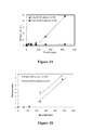
Figure 5 shows (a) the growth per cycle (GPC) of the PE-ALD Ru processes using various plasmas; (b) sheet resistance as function of thickness for Ru films deposited with various plasmas. -
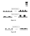
Figures 6 (a), (b), (c) illustrate schematically a few non-limitative examples wherein selective growth of Ru according to the method of the disclosure can be applied to simplify various device manufacturing flows. - The present disclosure will be described with respect to particular embodiments and with reference to certain drawings but the disclosure is not limited thereto but only by the claims. The drawings described are only schematic and are non-limiting. In the drawings, the size of some of the elements may be exaggerated and not drawn on scale for illustrative purposes. The dimensions and the relative dimensions do not necessarily correspond to actual reductions to practice of the disclosure.
- Furthermore, the terms first, second, third and the like in the description and in the claims, are used for distinguishing between similar elements and not necessarily for describing a sequential or chronological order. The terms are interchangeable under appropriate circumstances and the embodiments of the disclosure can operate in other sequences than described or illustrated herein.
- Moreover, the terms top, bottom, over, under and the like in the description and the claims are used for descriptive purposes and not necessarily for describing relative positions. The terms so used are interchangeable under appropriate circumstances and the embodiments of the disclosure described herein can operate in other orientations than described or illustrated herein.
- Furthermore, the various embodiments, although referred to as "preferred" are to be construed as exemplary manners in which the disclosure may be implemented rather than as limiting the scope of the disclosure.
- The term "comprising", used in the claims, should not be interpreted as being restricted to the elements or steps listed thereafter; it does not exclude other elements or steps. It needs to be interpreted as specifying the presence of the stated features, integers, steps or components as referred to, but does not preclude the presence or addition of one or more other features, integers, steps or components, or groups thereof. Thus, the scope of the expression "a device comprising A and B" should not be limited to devices consisting only of components A and B, rather with respect to the present disclosure, the only enumerated components of the device are A and B, and further the claim should be interpreted as including equivalents of those components.
- State of the art chemistry to deposit ruthenium by plasma enhanced atomic layer deposition (PE-ALD) is bis(ethylcyclopentadienyl)Ru or Ru(EtCp)2. However, the reported growth per cycle as well as the initial growth behavior varies strongly. This is likely due to the extreme sensitivity of the ALD Ru process to the substrate preparation and/or process specific conditions such as precursor dose and effective reactor temperature.
- In general, ALD growth of Ru on Si oxides surfaces suffers from a large incubation period. Eventually nucleation at isolated sites occurs with island growth as a result. Typically, applying a plasma pretreatment on the surface prior to Ru deposition can create more reactive sites towards the Ru(EtCp)2 precursor thereby reducing the incubation time. Whereas large incubation is reported on SiO2 substrates, metal nitrides are typically reported as better substrates from nucleation point of view. Consistently state of the art reports very short times to no incubation time on TiN substrates. The very short to no incubation times on TiN substrates are reported irrespective of the gasses present in PE-ALD reactor when exposing the substrate to the plasma. Both in the presence of e.g. Ar/NH3 and Ar/N2/H2 short to no incubation times of Ru on TiN are reported. It would be therefore expected that any mixture of these gasses would not lead to a different behavior in the initial growth on TiN.
- Moreover, the longer incubation time on SiO2 than on metal oxide or nitride substrates has been used in state of the art for selective growth of Ru on specific areas of a device, such as electrode. Thus, the selective growth is triggered in the state of the art by the nature of the substrate.
- In various embodiments the disclosure describes a method for depositing by PE-ALD a noble metal (ruthenium)-comprising layer whereby the incubation time with respect to a substrate is controlled by the plasma species that are present in the PE-ALD chamber during the deposition cycle of the noble metal (ruthenium)-comprising layer.
- Throughout the disclosure Plasma enhanced ALD refers either to the "direct plasma" configuration or to the "remote plasma" configuration, both suitable to be applied in the method of the disclosure.
- Advantageously by changing the plasma composition the selectivity of the noble metal (ruthenium) deposition/growth is changed with respect to a substrate, i.e. an initial selective growth can be turned into a non-selective growth and vice-versa, without taking the substrate out from the deposition chamber.
- In different embodiments of the disclosure, when depositing Ru using a N2/NH3 plasma a very large incubation period was observed on metal nitride substrates (TiN, TaN), while nearly no incubation is observed on Ru-based substrates (Ru, Ru(Ta)) for the same deposition process, i.e. for the same plasma composition and sequence of steps in the deposition cycle.
- When depositing Ru using a N2/H2 plasma, ruthenium growth is observed on metal nitrides (TiN, TaN) after a short incubation period. This short incubation period can be further tuned (made shorter/longer) by adapting amount of Ru precursor provided in the chamber (i.e. the Ru precursor pulse length). No incubation is observed for the same conditions (N2/H2 plasma) on Ru-based substrates (Ru, Ru(Ta)).
- These findings can be applied for the selective growth of PE-ALD Ru on substrates comprising metal nitride and Ru-based materials by using N2/NH3 plasma that enables the deposition of Ru on top of Ru-based substrates, while showing a very large incubation period on metal nitride substrates.
- It is further disclosed that by modifying the composition of the plasma from N2/NH3 to N2/H2, one can initiate the growth on the metal nitride and as such switch from a selective deposition to a non-selective one. Advantageously modifying the plasma composition can take place while the substrate is kept in the deposition chamber.
- In embodiments of the disclosure an additional plasma treatment is performed when switching from the N2/NH3 composition to the N2/H2 composition. The additional plasma treatment is aimed to reactivate the surface de-activated by the N2/NH3 plasma and thereby prepare the surface for the non-selective deposition with N2/H2. The additional plasma treatment is a N2, H2 or H2/H2 plasma or inert gas plasma such as Ar or He. The plasma treatment may be performed before starting the non-selective deposition cycle with N2 and/or H2 plasma.
- The switch in growth selectivity with respect to metal nitride surfaces can be applied to fill complex structures with a Ru-comprising material by simply changing the plasma composition during the growth, i.e. replacing NH3 with H2. For example, 3D structures can be filled taking advantage of the ALD conformality and switch in selectivity with respect to metal nitrides, replacing thereby several patterning steps.
- In specific embodiments Ru thin films were deposited by PE-ALD in a 300 mm ALD chamber with direct plasma capability. The plasma is generated between the substrate and the showerhead using a high frequency generator. The power is typically 400W and can be varied within a range from 50W to 600W, or within the more limited range from 100W to 600W. The ALD chamber is attached to a multiple chamber platform. The pressure in the chamber during ALD deposition was 3.5 Torr and the wafer temperature was kept at 330 °C unless mentioned otherwise. The temperature in the chamber during ALD deposition can be varied within a range from 200 °C -450 °C.
- Prior to the deposition, the substrates were optionally degassed for 1 minute in an Ar ambient at 350 °C and low pressure (about 2 Torr). The degas step is performed in an anneal chamber attached to the same platform.
- The method of the disclosure can be performed with any Ru precursor comprising bis-cyclopentadienyl and having none, 1 or more alkyl (methyl, ethyl, n-propyl, n-butyl, i-propyl, i-butyl, t-butyl, neopentyl, allyl, trimethylsilyl) substituents. Alternatively, other noble metals such as Rh, Pd, Os, Ir or Pt can be deposited using the method of the disclosure using a noble metal precursor comprising cyclopentadienyl and an alkyl substituent.
- For supplying the Ru or noble metal precursor into the PE-ALD chamber nitrogen (N2) is used as carrier gas. In specific embodiments Ru(EtCp)2 was used as Ru-source which is a substance in liquid state. Alternatively the Ru (or other noble metal) source can be a substance in solid or gas phase. The carrier gas (N2) passed through a bubbler containing Ru(EtCp)2 at a temperature of 50 °C which was sufficient to saturate the ALD process.
- Both N2 and one of NH3 or H2 are supplied continuously to the PE-ALD chamber during the deposition cycle as shown schematically in
Fig 1(a) and (b) . Alternatively, instead of N2, a mixture of N2 and an inert gas such as Ar or He can be supplied continuously. - For the selective deposition of Ru (or other noble metal) on a noble metal surface while no deposition/growth is performed on a metal nitride surface ammonia was supplied additionally to the chamber during the whole cycle. Plasma exposure was performed in the presence of nitrogen and ammonia (N2/NH3) either before supplying the Ru-precursor or after supplying and purging the Ru-precursor.
- For the non-selective deposition of Ru (or other noble metal) on noble metal surface and metal nitride surface plasma exposure was performed in the presence of nitrogen and hydrogen (N2/H2) either before supplying the Ru-precursor or after supplying and purging the Ru-precursor.
- In different embodiments the total pressure (process pressure) in the PE-ALD chamber was 3.5 Torr. For this process pressure, the partial pressure of NH3 can be varied between 0.04 Torr up to about 3.2 Torr, or alternatively between 0.1Torr and 2.5 Torr, or also between 0.4 Torr and 1.5Torr. In the particular examples shown in
Fig 4 the partial pressure of NH3 was selected to be 0.4 Torr, 0.9 Torr and, respectively 1.5 Torr. - Alternatively, for a process pressure of 3.5 Torr in the PE-ALD chamber, the partial pressure of H2 can be varied between 0.1 Torr up to about 1 Torr, or within the more limited range between 0.2 Torr and 0.5 Torr. In the particular examples shown in
Fig 4 the partial pressure of H2 was selected to be 0.2 Torr, and 0.5 Torr. - In different embodiments of the disclosure the NH3 flow is between 250sccm to 1500sccm, and in one embodiment, 750sccm. In different embodiments of the disclosure the H2 flow is between 150sccm to 450sccm, with one embodiment being 300sccm.
-
Figure 1 shows schematically the PE-ALD Ru cycle for Ru selective/non-selective deposition according to a method of the disclosure: (a) plasma strike after providing Ru-precursor and purge in the presence of N2/NH3 (selective) or N2/H2 (non-selective); (b) plasma strike before providing Ru-precursor in the presence of N2/NH3 (selective) or N2/H2 (non-selective). - In the embodiments wherein the growth is non-selective the plasma exposure is performed in a N2/H2 ambient.
- A purge may also be performed after the plasma strike and exposure to the second reactant (N2/NH3 or N2/H2). However, adding a purge after the second reactant does not influence the results. Due to the short life time of the excited species and the plasma generation at the wafer level (direct plasma), the purge after the plasma strike can be omitted since the byproducts are removed during the plasma pulse.
- In specific embodiments the substrate is a Si wafer. Substrates comprising other semiconductor materials or material compatible with semiconductor manufacturing can be used.
- According to embodiments of the disclosure, 10 nm TiN layer was deposited ex-situ by physical vapor deposition (PVD) on a Si wafer forming the herein further labeled 'metal nitride substrate'. In some other examples an in-situ PE-ALD TiN formed with tetrakis(dimethylamino)titanium (TDMAT)-precursor and N2/H2 plasma is used.
- A metal nitride substrate comprises TiN, TaN, WN or any mixtures or alloys thereof. In alternative embodiments AlN can be used. The metal nitrides are either stoichiometric or non-stoichiometric compounds. Alternatively the metal nitride substrate can comprise a metal which can be easily converted (or at least a top layer thereof can be easily converted) to metal nitride, by e.g. a plasma nitridation process, also referred to as "nitridable" metal. Non-limiting examples of such nitridable metals are Ti, Ta W, Al and any mixtures or alloys thereof. A metal nitride substrate may comprise further other elements such as carbon and/or oxygen.
- In some examples, a Ru-CVD seed or Ru-rich PVD Ru(Ta) layer was deposited on top of the TiN substrates prior to PE-ALD Ru deposition thereby forming the 'Ru-based substrates'. The Ru/Ta atomic ratio was about 10/1.
- In the context of the present disclosure other noble metal substrates or substrates comprising an upper layer of metals like Cu which cannot be easily nitrided will behave similarly with the Ru-based substrate.
- In other embodiments of the disclosure, 20 nm thermally grown SiO2 substrates (on a Si wafer) also referred to 'as silicon oxide substrates' were formed. Alternatively the 'silicon oxide substrate' may comprise SiON.
- The thickness of the Ru films and their within wafer non-uniformity (WiWNU) was determined by spectroscopic ellipsometry (SE) using a KLA-Tencor™ Aleris. 49 point maps with 10 mm edge exclusions were collected. In this way Ru films up to 10 nm on 10 nm TiN substrates could be measured reliably. The thickness limitation is set by the limited penetration depth of light in metals.
- Film thickness values were also determined by x-ray reflectometry with a Jordan Valley™ x-ray diffractometer using Cu Kα radiation. The same diffractometer was used to assess the crystallinity by x-ray diffraction (XRD). The sheet resistance (Rs) was measured using an Rs100 KLA-Tencor™ 4-points prober.
- Impurity levels were measured by time of flight secondary ion mass spectroscopy (ToFSIMS) using an ION-TOF-IV instrument with a Ga source operating at a beam energy of 15 keV (area of 80 x 80 µm2) for analysis and a Xe beam with an energy of 350eV (sputter area of 500x500 µm2) for depth profiling. Rutherford backscattering (RBS) using a 1 MeV He+ beam was used to determine the deposited amount of metal atoms.
- On Ru-based substrates (Ru seed or RuTa), Ru-growth shows a linear behavior for PE-ALD using N2/NH3 plasma. No significant incubation was observed, as shown in
Figure 2(a) . - On TiN-substrates a very long incubation of Ru growth, i.e. more than 480 cycles, was found, as shown in
Figure 2(b) . Even for very long precursor Ru(EtCp)2 pulse times (i.e. 10x longer), and high source temperature (Ru ampoule at 35 °C and higher), no significant growth was obtained the first 480 cycles. Similarly large incubation times were observed on TaN substrates. The effect observed is very pronounced and 'tuning' the incubation time by increasing the amount of precursor provided does not lead to any significant growth. - In the presence of N2/NH3 plasma, the incubation time of Ru growth on the metal nitride substrates was even larger than that on SiO2 substrates as can be concluded when comparing
Figs 2(b) and2(c) . This is highly unexpected in the light of the state of the art which typically reports an opposite behavior. Although the growth on SiO2 shows a significant incubation, the incubation period is still sufficiently different from that on TiN in presence of N2/NH3, thereby allowing selective deposition on SiO2 while no growth is observed on TiN. - A similarly large incubation was found for Ru growth with N2/NH3 plasma process on in-situ deposited TiN from TDMAT and N2/H2 plasma. In this particular example, there is no O contamination on the TiN surface due to air exposure as might be the case for the ex-situ formed TiN with formation of an oxidized TiN. Therefore O contamination on the TiN surface as growth inhibition factor can be excluded.
- Thus, in different embodiments, Ru growth from Ru(EtCp)2 was performed using a N2/NH3 plasma on Ru-based substrates, while no growth was observed on metal nitride and oxidized metal nitride substrates.
- The same behavior was found after a pretreatment with N2/HH3 plasma (prior to supplying the Ru precursor in the chamber) as shown in
Figure 1(b) . Without wishing to be bound by theory we believe this indicates that the incubation inhibition is due to a hinder in the absorption/chemisorption of Ru(EtCp)2 on the TiN substrates after exposure to a N2/NH3 plasma before or after supplying and purging the Ru (or other noble metal) precursor in the chamber. - The selective growth on metal (Ru) with respect to metal nitride (TiN) was demonstrated by having a wafer which is already covered with TiN partially covered with a thin Ru seed. At edge areas of the wafer, the Ru seed was lacking. About 11 nm PE-ALD Ru deposition could be obtained on the area where the seed is present, whereas no deposition is obtained where the seed is not present, as shown in
Figure 2(d) . A similar deposition process on a uniformly deposited Ru seed showed a uniform PE-ALD Ru deposition from center to edge. - When replacing in the experiments above the N2/NH3 plasma, with N2/H2 plasma different results are obtained. Ru deposition can be obtained on TiN substrates as shown in
Figure 3(a) . When comparing the impact of the plasma on SiO2 substrates (Figure 3(b) ), a similar trend has been observed as on TiN. Comparing with N2/NH3 plasma, N2/H2 plasma on SiO2 substrates leads to shorter incubation times. Although, the difference in incubation time on SiO2 is smaller than on TiN substrates, it illustrates the effect of plasma selection used during the ALD growth of Ru (or any other noble metal) on the incubation time. - The incubation time can be tuned by increasing the Ru exposure per ALD cycle as shown in
Figure 3(c) . A low and high dose of Ru/pulse was obtained by changing the Ru ampoule temperature from 50 °C to 85 °C, respectively. This corresponds to a ∼10x increase in vapor pressure which is a measure of the Ru dose. All the other parameters such as pulse, purge times were kept fixed. - A N2/H2 plasma pretreatment prior to Ru deposition did not significantly reduce the inhibition observed in the case of deposition by N2/NH3 plasma.
- Differences in growth incubation are typically attributed to differences in active sites on substrate on which the Ru(EtCp)2 chemisorbs after the plasma exposure. In that case, N2/H2 plasma would be more effective than N2/NH3 to create these active sites. A plasma pretreatment with the effective N2/H2 should create these active sites. However, we have observed similarly long incubation times for N2/NH3 plasma on TiN substrates that have undergone first a N2/H2 plasma treatment similar to the plasma exposure the wafers receive during the first 40 and 120 cycles of the Ru deposition with N2/H2 plasma. There was no air break between the plasma treatment and subsequent Ru deposition with N2/NH3 plasma. Surprisingly, no significant difference was observed with respect to the samples which were not treated first with N2/H2 plasma. The latter suggests that if reactive sites were present after the N2/H2 plasma treatment, the N2/NH3 plasma has deactivated them.
- In
Figure 4 , the impact of the plasma composition (from N2/NH3 1500sccm towards N2/H2 450sccm) on the Ru thickness after 240 ALD cycles on TiN substrates is shown. As soon as NH3 is added to the N2, very long incubation occurs. - For pure N2 ALD growth was observed without incubation, but the growth per cycle (GPC) was reduced suggesting that pure N2 plasma is less suited to remove the ligands from the Ru precursor, possibly resulting in less dense films and more C impurities. For pure N2 plasma, the resistivity is also higher in agreement with less dense, less pure layers as shown in
Figure 5(b) . As soon as H2 plasma is added, the expected thickness is obtained indicating that activated H species a more effective to remove the ligands. - When switching the plasma composition from N2/NH3 and N2/H2 no difference has been found in the growth per cycle values of Ru. GPC of about 0.016 nm is found for both N2/NH3 (on RuTa/TiN) and N2/H2 plasma (on TiN) as shown in
Figure 5(a) . A higher precursor dose, longer plasma exposure, or higher plasma power (data not shown) did not significantly influence the GPC or resistivity indicating that the process is saturated. The only parameter that influenced the GPC was the reactor temperature. An increase in GPC to about 0.025 nm with increasing temperature up to about 400°C was found. Note that for N2 plasma (on TiN) a lower GPC was found as already discussed above. - The resistivity of the Ru films deposited by N2/NH3 and N2/H2 plasma is similar, even besides the ultra-thin film range, as shown in
Figure 5(b) . Therefore switching the plasma composition from N2/NH3 and N2/H2 does not lead to differences in the quality (physical properties) of the Ru layer formed. For N2 plasma, the resistivity is higher. This is likely due to more in-film impurities due to incomplete surface reactions. This suggests that the physical properties of the deposited Ru films are similar. XRD patterns show in all cases polycrystalline hexagonal Ru films. Thicker films show texture along the (101) direction on TiN. -
Figure 6 illustrates schematically few non-limitative examples wherein selective growth of Ru according to the method of the disclosure can be applied to simplify various process flows: (a) selective growth of Ru (red) on top of Ru-comprising material (red), bottom up fill of a patterned structure defined in TiN (blue) or pillars grown on top of predefined Ru dots/structures on a TiN substrate (blue); (b) selective grown of Ru (red) on SiO2 (light green), bottom up fill with Ru of patterned structure defined in TiN, (c) Ru T-shape structures grown by PE-ALD by modifying the plasma composition according to the method of the disclosure, possibly without taking the substrate out of the PE-ALD chamber. - The various process flows referred above can be any manufacturing flows of a semiconductor device such as DRAM, MIMCAP, RRAM, interconnect metallization of advanced scaled devices as well as any other application wherein Ru selective growth and/or a switch between selective and non-selective growth can be advantageously applied.
Claims (15)
- A method for forming a noble metal layer by Plasma Enhanced Atomic Layer Deposition, PE-ALD, comprising the steps of:- providing a substrate in a PE-ALD chamber, the substrate comprising a first region having an exposed first material and a second region having an exposed second material, wherein the first material comprises a metal nitride or a nitridable metal, and the second material comprises a non-nitritable metal or silicon oxide;- selective deposition by PE-ALD of a noble metal layer on the second region, by repeatedly performing a deposition cycle comprising the following steps:(a) supplying a noble metal precursor to the PE-ALD chamber and contacting the noble metal precursor with the substrate in the presence of a carrier gas followed by purging the noble metal precursor, and(b) exposing the substrate to plasma in the PE-ALD chamber while supplying ammonia and the carrier gas into the PE-ALD chamber.
- The method according to claim 1, wherein the deposition cycle is performed with step (a) as the first step.
- The method according to claim 1, wherein the deposition cycle is performed with step (b) as the first step.
- The method according to claims 1-3, further comprising after the selective deposition, performing a non-selective deposition by PE-ALD of a noble metal layer on the second region and on the first region, by repeatedly performing the deposition cycle wherein at step (b) the ammonia is replaced by hydrogen (H2).
- The method according to claims 4, wherein the non-selective deposition is performed after the selective deposition in the same PE-ALD chamber while the substrate is kept in the chamber.
- The method according to any of the claims 4 or 5, further comprising performing an additional plasma treatment of the substrate prior to the non-selective deposition of the noble metal layer.
- The method according to claim 6, wherein the additional plasma treatment is a N2, H2 or H2/H2 plasma or inert gas plasma such as Ar or He.
- The method according to any one of the preceding claims, wherein the carrier gas is N2 or a mixture of N2 and an inert gas such as Ar or He.
- The method according to any one of the preceding claims, characterized in that the noble metal comprises Ru, Rh, Pd, Os, Ir or Pt.
- The method according to claim 9, wherein the noble metal is Ru or RuTa alloy.
- The method according to any one of the preceding claims, characterized in that the metal nitride comprises TiN, TaN or WN.
- The method according to claim 11, characterized in that the metal nitride comprises further carbon and/or oxygen.
- The method according to any one of the preceding claims, wherein the nitridable metals are selected from the group of Ti, Ta, W, Al and any mixtures or alloys thereof.
- The method according to any one of the preceding claims, characterized in that during the deposition cycle, the PE-ALD chamber may be continuously supplied with nitrogen and one of ammonia or hydrogen.
- The method according to any one of the preceding claims, characterized in that the noble metal precursor is chosen from the group consisting of: bis(ethylcyclopentadienyl)Me and bis(cyclopentadienyl)Me having one or more alkyl substituents.
Applications Claiming Priority (1)
| Application Number | Priority Date | Filing Date | Title |
|---|---|---|---|
| US201161542876P | 2011-10-04 | 2011-10-04 |
Publications (2)
| Publication Number | Publication Date |
|---|---|
| EP2578723A1 true EP2578723A1 (en) | 2013-04-10 |
| EP2578723B1 EP2578723B1 (en) | 2015-05-06 |
Family
ID=47010334
Family Applications (1)
| Application Number | Title | Priority Date | Filing Date |
|---|---|---|---|
| EP20120187296 Active EP2578723B1 (en) | 2011-10-04 | 2012-10-04 | Method for selectively depositing noble metals on metal/metal nitride substrates |
Country Status (3)
| Country | Link |
|---|---|
| US (1) | US8921228B2 (en) |
| EP (1) | EP2578723B1 (en) |
| JP (1) | JP6116849B2 (en) |
Families Citing this family (41)
| Publication number | Priority date | Publication date | Assignee | Title |
|---|---|---|---|---|
| TWI661072B (en) | 2014-02-04 | 2019-06-01 | 荷蘭商Asm Ip控股公司 | Selective deposition of metals, metal oxides, and dielectrics |
| US9425078B2 (en) * | 2014-02-26 | 2016-08-23 | Lam Research Corporation | Inhibitor plasma mediated atomic layer deposition for seamless feature fill |
| US10047435B2 (en) | 2014-04-16 | 2018-08-14 | Asm Ip Holding B.V. | Dual selective deposition |
| CN106537510B (en) | 2014-04-30 | 2019-03-01 | 慧与发展有限责任合伙企业 | Resistive memory device with multi-component electrodes |
| WO2016120957A1 (en) * | 2015-01-26 | 2016-08-04 | 株式会社日立国際電気 | Semiconductor-device manufacturing method, substrate treating apparatus, and recording medium |
| US9490145B2 (en) | 2015-02-23 | 2016-11-08 | Asm Ip Holding B.V. | Removal of surface passivation |
| US10428421B2 (en) | 2015-08-03 | 2019-10-01 | Asm Ip Holding B.V. | Selective deposition on metal or metallic surfaces relative to dielectric surfaces |
| US10790141B2 (en) | 2015-09-19 | 2020-09-29 | Applied Materials, Inc. | Surface-selective atomic layer deposition using hydrosilylation passivation |
| JP6417051B2 (en) * | 2015-09-29 | 2018-10-31 | 株式会社Kokusai Electric | Semiconductor device manufacturing method, substrate processing apparatus, and program |
| US10814349B2 (en) | 2015-10-09 | 2020-10-27 | Asm Ip Holding B.V. | Vapor phase deposition of organic films |
| US10695794B2 (en) | 2015-10-09 | 2020-06-30 | Asm Ip Holding B.V. | Vapor phase deposition of organic films |
| US11028477B2 (en) | 2015-10-23 | 2021-06-08 | Applied Materials, Inc. | Bottom-up gap-fill by surface poisoning treatment |
| US10192775B2 (en) | 2016-03-17 | 2019-01-29 | Applied Materials, Inc. | Methods for gapfill in high aspect ratio structures |
| US11081342B2 (en) | 2016-05-05 | 2021-08-03 | Asm Ip Holding B.V. | Selective deposition using hydrophobic precursors |
| US10373820B2 (en) | 2016-06-01 | 2019-08-06 | Asm Ip Holding B.V. | Deposition of organic films |
| US10453701B2 (en) | 2016-06-01 | 2019-10-22 | Asm Ip Holding B.V. | Deposition of organic films |
| RU2633894C1 (en) * | 2016-06-24 | 2017-10-19 | Акционерное общество "Научно-производственное предприятие "Пульсар" | Method of plasma-stimulated atomic-layer deposition of insulating dielectric coatings on heterostructures of nitrid-gallium semiconductor devices |
| US20180053688A1 (en) * | 2016-08-16 | 2018-02-22 | Tokyo Electron Limited | Method of metal filling recessed features in a substrate |
| US11430656B2 (en) | 2016-11-29 | 2022-08-30 | Asm Ip Holding B.V. | Deposition of oxide thin films |
| US10176984B2 (en) | 2017-02-14 | 2019-01-08 | Lam Research Corporation | Selective deposition of silicon oxide |
| JP7169072B2 (en) | 2017-02-14 | 2022-11-10 | エーエスエム アイピー ホールディング ビー.ブイ. | Selective passivation and selective deposition |
| US10242866B2 (en) | 2017-03-08 | 2019-03-26 | Lam Research Corporation | Selective deposition of silicon nitride on silicon oxide using catalytic control |
| US10043656B1 (en) * | 2017-03-10 | 2018-08-07 | Lam Research Corporation | Selective growth of silicon oxide or silicon nitride on silicon surfaces in the presence of silicon oxide |
| US9911595B1 (en) | 2017-03-17 | 2018-03-06 | Lam Research Corporation | Selective growth of silicon nitride |
| US10559461B2 (en) | 2017-04-19 | 2020-02-11 | Lam Research Corporation | Selective deposition with atomic layer etch reset |
| US11501965B2 (en) | 2017-05-05 | 2022-11-15 | Asm Ip Holding B.V. | Plasma enhanced deposition processes for controlled formation of metal oxide thin films |
| JP7183187B2 (en) * | 2017-05-16 | 2022-12-05 | エーエスエム アイピー ホールディング ビー.ブイ. | Selective PEALD of oxides on dielectrics |
| CN111032908B (en) * | 2017-06-23 | 2024-01-30 | 默克专利有限公司 | Atomic layer deposition method for selective film growth |
| US10460930B2 (en) | 2017-11-22 | 2019-10-29 | Lam Research Corporation | Selective growth of SiO2 on dielectric surfaces in the presence of copper |
| US11404275B2 (en) | 2018-03-02 | 2022-08-02 | Lam Research Corporation | Selective deposition using hydrolysis |
| JP2020056104A (en) | 2018-10-02 | 2020-04-09 | エーエスエム アイピー ホールディング ビー.ブイ. | Selective passivation and selective deposition |
| US12482648B2 (en) | 2018-10-02 | 2025-11-25 | Asm Ip Holding B.V. | Selective passivation and selective deposition |
| US11965238B2 (en) | 2019-04-12 | 2024-04-23 | Asm Ip Holding B.V. | Selective deposition of metal oxides on metal surfaces |
| US11133178B2 (en) | 2019-09-20 | 2021-09-28 | Applied Materials, Inc. | Seamless gapfill with dielectric ALD films |
| US11139163B2 (en) | 2019-10-31 | 2021-10-05 | Asm Ip Holding B.V. | Selective deposition of SiOC thin films |
| WO2021187485A1 (en) * | 2020-03-18 | 2021-09-23 | 東ソー株式会社 | Method for producing metal-containing thin film, and metal-containing thin film |
| TWI865747B (en) | 2020-03-30 | 2024-12-11 | 荷蘭商Asm Ip私人控股有限公司 | Simultaneous selective deposition of two different materials on two different surfaces |
| TWI862807B (en) | 2020-03-30 | 2024-11-21 | 荷蘭商Asm Ip私人控股有限公司 | Selective deposition of silicon oxide on dielectric surfaces relative to metal surfaces |
| TW202140832A (en) | 2020-03-30 | 2021-11-01 | 荷蘭商Asm Ip私人控股有限公司 | Selective deposition of silicon oxide on metal surfaces |
| CN117467975B (en) * | 2023-10-11 | 2026-01-02 | 西安近代化学研究所 | Method for preparing metal films on quartz substrates based on metal transition layers |
| KR102957923B1 (en) * | 2023-10-19 | 2026-04-27 | 한국과학기술연구원 | Area-selective growth method for noble metal thin films using atomic layer deposition |
Citations (1)
| Publication number | Priority date | Publication date | Assignee | Title |
|---|---|---|---|---|
| US20100136776A1 (en) | 2005-03-15 | 2010-06-03 | Asm International N.V. | Selective deposition of noble metal thin films |
Family Cites Families (7)
| Publication number | Priority date | Publication date | Assignee | Title |
|---|---|---|---|---|
| US7279423B2 (en) * | 2002-10-31 | 2007-10-09 | Intel Corporation | Forming a copper diffusion barrier |
| US7186446B2 (en) | 2003-10-31 | 2007-03-06 | International Business Machines Corporation | Plasma enhanced ALD of tantalum nitride and bilayer |
| US7476618B2 (en) * | 2004-10-26 | 2009-01-13 | Asm Japan K.K. | Selective formation of metal layers in an integrated circuit |
| KR101379015B1 (en) * | 2006-02-15 | 2014-03-28 | 한국에이에스엠지니텍 주식회사 | METHOD OF DEPOSITING Ru FILM USING PEALD AND DENSE Ru FILM |
| JP2008205325A (en) * | 2007-02-22 | 2008-09-04 | Hitachi Kokusai Electric Inc | Semiconductor device manufacturing method and substrate processing apparatus |
| US7829454B2 (en) | 2007-09-11 | 2010-11-09 | Tokyo Electron Limited | Method for integrating selective ruthenium deposition into manufacturing of a semiconductior device |
| US7939421B2 (en) * | 2009-07-08 | 2011-05-10 | Nanya Technology Corp. | Method for fabricating integrated circuit structures |
-
2012
- 2012-10-03 US US13/644,075 patent/US8921228B2/en active Active
- 2012-10-04 EP EP20120187296 patent/EP2578723B1/en active Active
- 2012-10-04 JP JP2012221882A patent/JP6116849B2/en active Active
Patent Citations (1)
| Publication number | Priority date | Publication date | Assignee | Title |
|---|---|---|---|---|
| US20100136776A1 (en) | 2005-03-15 | 2010-06-03 | Asm International N.V. | Selective deposition of noble metal thin films |
Non-Patent Citations (2)
| Title |
|---|
| SWERTS J ET AL: "Scalability of plasma enhanced atomic layer deposited ruthenium films for interconnect applications", JOURNAL OF VACUUM SCIENCE & TECHNOLOGY A (VACUUM, SURFACES, AND FILMS) PUBLISHED FOR THE AMERICAN VACUUM SOCIETY BY THE AMERICAN INSTITUTE OF PHYSICS USA, vol. 30, no. 1, 2 September 2011 (2011-09-02), US, pages 01A103-1 - 01A103-6, XP002690473, ISSN: 0734-2101 * |
| YIM SUNG-SOO ET AL: "Nucleation kinetics of Ru on silicon oxide and silicon nitride surfaces deposited by atomic layer deposition", JOURNAL OF APPLIED PHYSICS, AMERICAN INSTITUTE OF PHYSICS. NEW YORK, US, vol. 103, no. 11, 10 June 2008 (2008-06-10), pages 113509 - 113509, XP012108860, ISSN: 0021-8979, DOI: 10.1063/1.2938052 * |
Also Published As
| Publication number | Publication date |
|---|---|
| US20130084700A1 (en) | 2013-04-04 |
| JP6116849B2 (en) | 2017-04-19 |
| JP2013079447A (en) | 2013-05-02 |
| EP2578723B1 (en) | 2015-05-06 |
| US8921228B2 (en) | 2014-12-30 |
Similar Documents
| Publication | Publication Date | Title |
|---|---|---|
| EP2578723B1 (en) | Method for selectively depositing noble metals on metal/metal nitride substrates | |
| US7595270B2 (en) | Passivated stoichiometric metal nitride films | |
| KR101540077B1 (en) | Atomic layer deposition of metal carbide films using aluminum hydrocarbon compounds | |
| US7220451B2 (en) | Process for producing metal thin films by ALD | |
| US7160817B2 (en) | Dielectric material forming methods | |
| US7713874B2 (en) | Periodic plasma annealing in an ALD-type process | |
| KR101506019B1 (en) | Vapor deposition of metal carbide film | |
| US7550385B2 (en) | Amine-free deposition of metal-nitride films | |
| TW201936980A (en) | Deposition method | |
| TW201728779A (en) | NbMC layer | |
| US20060177601A1 (en) | Method of forming a ruthenium thin film using a plasma enhanced atomic layer deposition apparatus and the method thereof | |
| KR20140112440A (en) | Deposition of smooth metal nitride films | |
| KR20170001617A (en) | Structures including metal carbide material, devices including the structures, and methods of forming same | |
| TW201142946A (en) | NMOS metal gate materials, manufacturing methods, and equipment using CVD and ALD processes with metal based precursors | |
| Choi et al. | Thermal atomic layer deposition (ALD) of Ru films for Cu direct plating | |
| KR20170017779A (en) | Selective deposition of aluminum and nitrogen containing material | |
| TW202115270A (en) | Group vi metal deposition process | |
| Jeon et al. | Chemistry of active oxygen in RuO x and its influence on the atomic layer deposition of TiO 2 films | |
| WO2011159691A2 (en) | Chemical vapor deposition of ruthenium films containing oxygen or carbon | |
| US7808106B1 (en) | Nano-laminate difussion barrier for direct electrochemical deposition copper | |
| US7183649B1 (en) | Methods and procedures for engineering of composite conductive films by atomic layer deposition | |
| US7129580B1 (en) | Methods and procedures for engineering of composite conductive films by atomic layer deposition | |
| Swerts et al. | Plasma Enhanced Atomic Layer Deposited Ruthenium for MIMCAP Applications | |
| Kim et al. | Suppression of interfacial layers in ZrO 2/TiN capacitors by atomic layer deposition using ligand-engineered Zr precursors for scalable DRAM | |
| Matsushita et al. | b IBM, Fishkill, New York, 12533, USA |
Legal Events
| Date | Code | Title | Description |
|---|---|---|---|
| PUAI | Public reference made under article 153(3) epc to a published international application that has entered the european phase |
Free format text: ORIGINAL CODE: 0009012 |
|
| AK | Designated contracting states |
Kind code of ref document: A1 Designated state(s): AL AT BE BG CH CY CZ DE DK EE ES FI FR GB GR HR HU IE IS IT LI LT LU LV MC MK MT NL NO PL PT RO RS SE SI SK SM TR |
|
| AX | Request for extension of the european patent |
Extension state: BA ME |
|
| 17P | Request for examination filed |
Effective date: 20131010 |
|
| RBV | Designated contracting states (corrected) |
Designated state(s): AL AT BE BG CH CY CZ DE DK EE ES FI FR GB GR HR HU IE IS IT LI LT LU LV MC MK MT NL NO PL PT RO RS SE SI SK SM TR |
|
| GRAP | Despatch of communication of intention to grant a patent |
Free format text: ORIGINAL CODE: EPIDOSNIGR1 |
|
| INTG | Intention to grant announced |
Effective date: 20150122 |
|
| GRAS | Grant fee paid |
Free format text: ORIGINAL CODE: EPIDOSNIGR3 |
|
| GRAA | (expected) grant |
Free format text: ORIGINAL CODE: 0009210 |
|
| AK | Designated contracting states |
Kind code of ref document: B1 Designated state(s): AL AT BE BG CH CY CZ DE DK EE ES FI FR GB GR HR HU IE IS IT LI LT LU LV MC MK MT NL NO PL PT RO RS SE SI SK SM TR |
|
| REG | Reference to a national code |
Ref country code: GB Ref legal event code: FG4D |
|
| REG | Reference to a national code |
Ref country code: CH Ref legal event code: EP |
|
| REG | Reference to a national code |
Ref country code: IE Ref legal event code: FG4D |
|
| REG | Reference to a national code |
Ref country code: AT Ref legal event code: REF Ref document number: 725766 Country of ref document: AT Kind code of ref document: T Effective date: 20150615 |
|
| REG | Reference to a national code |
Ref country code: DE Ref legal event code: R096 Ref document number: 602012007111 Country of ref document: DE Effective date: 20150618 |
|
| REG | Reference to a national code |
Ref country code: AT Ref legal event code: MK05 Ref document number: 725766 Country of ref document: AT Kind code of ref document: T Effective date: 20150506 |
|
| REG | Reference to a national code |
Ref country code: FR Ref legal event code: PLFP Year of fee payment: 4 |
|
| REG | Reference to a national code |
Ref country code: NL Ref legal event code: MP Effective date: 20150506 |
|
| REG | Reference to a national code |
Ref country code: LT Ref legal event code: MG4D |
|
| PG25 | Lapsed in a contracting state [announced via postgrant information from national office to epo] |
Ref country code: NO Free format text: LAPSE BECAUSE OF FAILURE TO SUBMIT A TRANSLATION OF THE DESCRIPTION OR TO PAY THE FEE WITHIN THE PRESCRIBED TIME-LIMIT Effective date: 20150806 Ref country code: PT Free format text: LAPSE BECAUSE OF FAILURE TO SUBMIT A TRANSLATION OF THE DESCRIPTION OR TO PAY THE FEE WITHIN THE PRESCRIBED TIME-LIMIT Effective date: 20150907 Ref country code: LT Free format text: LAPSE BECAUSE OF FAILURE TO SUBMIT A TRANSLATION OF THE DESCRIPTION OR TO PAY THE FEE WITHIN THE PRESCRIBED TIME-LIMIT Effective date: 20150506 Ref country code: ES Free format text: LAPSE BECAUSE OF FAILURE TO SUBMIT A TRANSLATION OF THE DESCRIPTION OR TO PAY THE FEE WITHIN THE PRESCRIBED TIME-LIMIT Effective date: 20150506 Ref country code: HR Free format text: LAPSE BECAUSE OF FAILURE TO SUBMIT A TRANSLATION OF THE DESCRIPTION OR TO PAY THE FEE WITHIN THE PRESCRIBED TIME-LIMIT Effective date: 20150506 Ref country code: FI Free format text: LAPSE BECAUSE OF FAILURE TO SUBMIT A TRANSLATION OF THE DESCRIPTION OR TO PAY THE FEE WITHIN THE PRESCRIBED TIME-LIMIT Effective date: 20150506 |
|
| PG25 | Lapsed in a contracting state [announced via postgrant information from national office to epo] |
Ref country code: IS Free format text: LAPSE BECAUSE OF FAILURE TO SUBMIT A TRANSLATION OF THE DESCRIPTION OR TO PAY THE FEE WITHIN THE PRESCRIBED TIME-LIMIT Effective date: 20150906 Ref country code: GR Free format text: LAPSE BECAUSE OF FAILURE TO SUBMIT A TRANSLATION OF THE DESCRIPTION OR TO PAY THE FEE WITHIN THE PRESCRIBED TIME-LIMIT Effective date: 20150807 Ref country code: AT Free format text: LAPSE BECAUSE OF FAILURE TO SUBMIT A TRANSLATION OF THE DESCRIPTION OR TO PAY THE FEE WITHIN THE PRESCRIBED TIME-LIMIT Effective date: 20150506 Ref country code: LV Free format text: LAPSE BECAUSE OF FAILURE TO SUBMIT A TRANSLATION OF THE DESCRIPTION OR TO PAY THE FEE WITHIN THE PRESCRIBED TIME-LIMIT Effective date: 20150506 Ref country code: RS Free format text: LAPSE BECAUSE OF FAILURE TO SUBMIT A TRANSLATION OF THE DESCRIPTION OR TO PAY THE FEE WITHIN THE PRESCRIBED TIME-LIMIT Effective date: 20150506 Ref country code: BG Free format text: LAPSE BECAUSE OF FAILURE TO SUBMIT A TRANSLATION OF THE DESCRIPTION OR TO PAY THE FEE WITHIN THE PRESCRIBED TIME-LIMIT Effective date: 20150806 |
|
| PG25 | Lapsed in a contracting state [announced via postgrant information from national office to epo] |
Ref country code: DK Free format text: LAPSE BECAUSE OF FAILURE TO SUBMIT A TRANSLATION OF THE DESCRIPTION OR TO PAY THE FEE WITHIN THE PRESCRIBED TIME-LIMIT Effective date: 20150506 Ref country code: EE Free format text: LAPSE BECAUSE OF FAILURE TO SUBMIT A TRANSLATION OF THE DESCRIPTION OR TO PAY THE FEE WITHIN THE PRESCRIBED TIME-LIMIT Effective date: 20150506 |
|
| REG | Reference to a national code |
Ref country code: DE Ref legal event code: R097 Ref document number: 602012007111 Country of ref document: DE |
|
| PG25 | Lapsed in a contracting state [announced via postgrant information from national office to epo] |
Ref country code: RO Free format text: LAPSE BECAUSE OF NON-PAYMENT OF DUE FEES Effective date: 20150506 Ref country code: PL Free format text: LAPSE BECAUSE OF FAILURE TO SUBMIT A TRANSLATION OF THE DESCRIPTION OR TO PAY THE FEE WITHIN THE PRESCRIBED TIME-LIMIT Effective date: 20150506 Ref country code: SK Free format text: LAPSE BECAUSE OF FAILURE TO SUBMIT A TRANSLATION OF THE DESCRIPTION OR TO PAY THE FEE WITHIN THE PRESCRIBED TIME-LIMIT Effective date: 20150506 Ref country code: CZ Free format text: LAPSE BECAUSE OF FAILURE TO SUBMIT A TRANSLATION OF THE DESCRIPTION OR TO PAY THE FEE WITHIN THE PRESCRIBED TIME-LIMIT Effective date: 20150506 |
|
| PLBE | No opposition filed within time limit |
Free format text: ORIGINAL CODE: 0009261 |
|
| STAA | Information on the status of an ep patent application or granted ep patent |
Free format text: STATUS: NO OPPOSITION FILED WITHIN TIME LIMIT |
|
| 26N | No opposition filed |
Effective date: 20160209 |
|
| PG25 | Lapsed in a contracting state [announced via postgrant information from national office to epo] |
Ref country code: IT Free format text: LAPSE BECAUSE OF FAILURE TO SUBMIT A TRANSLATION OF THE DESCRIPTION OR TO PAY THE FEE WITHIN THE PRESCRIBED TIME-LIMIT Effective date: 20150506 |
|
| PG25 | Lapsed in a contracting state [announced via postgrant information from national office to epo] |
Ref country code: LU Free format text: LAPSE BECAUSE OF FAILURE TO SUBMIT A TRANSLATION OF THE DESCRIPTION OR TO PAY THE FEE WITHIN THE PRESCRIBED TIME-LIMIT Effective date: 20151004 Ref country code: SI Free format text: LAPSE BECAUSE OF FAILURE TO SUBMIT A TRANSLATION OF THE DESCRIPTION OR TO PAY THE FEE WITHIN THE PRESCRIBED TIME-LIMIT Effective date: 20150506 |
|
| REG | Reference to a national code |
Ref country code: CH Ref legal event code: PL |
|
| PG25 | Lapsed in a contracting state [announced via postgrant information from national office to epo] |
Ref country code: MC Free format text: LAPSE BECAUSE OF FAILURE TO SUBMIT A TRANSLATION OF THE DESCRIPTION OR TO PAY THE FEE WITHIN THE PRESCRIBED TIME-LIMIT Effective date: 20150506 |
|
| REG | Reference to a national code |
Ref country code: IE Ref legal event code: MM4A |
|
| PG25 | Lapsed in a contracting state [announced via postgrant information from national office to epo] |
Ref country code: CH Free format text: LAPSE BECAUSE OF NON-PAYMENT OF DUE FEES Effective date: 20151031 Ref country code: LI Free format text: LAPSE BECAUSE OF NON-PAYMENT OF DUE FEES Effective date: 20151031 |
|
| PG25 | Lapsed in a contracting state [announced via postgrant information from national office to epo] |
Ref country code: BE Free format text: LAPSE BECAUSE OF FAILURE TO SUBMIT A TRANSLATION OF THE DESCRIPTION OR TO PAY THE FEE WITHIN THE PRESCRIBED TIME-LIMIT Effective date: 20150506 |
|
| REG | Reference to a national code |
Ref country code: FR Ref legal event code: PLFP Year of fee payment: 5 |
|
| PG25 | Lapsed in a contracting state [announced via postgrant information from national office to epo] |
Ref country code: IE Free format text: LAPSE BECAUSE OF NON-PAYMENT OF DUE FEES Effective date: 20151004 |
|
| PG25 | Lapsed in a contracting state [announced via postgrant information from national office to epo] |
Ref country code: SM Free format text: LAPSE BECAUSE OF FAILURE TO SUBMIT A TRANSLATION OF THE DESCRIPTION OR TO PAY THE FEE WITHIN THE PRESCRIBED TIME-LIMIT Effective date: 20150506 Ref country code: HU Free format text: LAPSE BECAUSE OF FAILURE TO SUBMIT A TRANSLATION OF THE DESCRIPTION OR TO PAY THE FEE WITHIN THE PRESCRIBED TIME-LIMIT; INVALID AB INITIO Effective date: 20121004 |
|
| GBPC | Gb: european patent ceased through non-payment of renewal fee |
Effective date: 20161004 |
|
| PG25 | Lapsed in a contracting state [announced via postgrant information from national office to epo] |
Ref country code: NL Free format text: LAPSE BECAUSE OF FAILURE TO SUBMIT A TRANSLATION OF THE DESCRIPTION OR TO PAY THE FEE WITHIN THE PRESCRIBED TIME-LIMIT Effective date: 20150506 Ref country code: CY Free format text: LAPSE BECAUSE OF FAILURE TO SUBMIT A TRANSLATION OF THE DESCRIPTION OR TO PAY THE FEE WITHIN THE PRESCRIBED TIME-LIMIT Effective date: 20150506 Ref country code: SE Free format text: LAPSE BECAUSE OF FAILURE TO SUBMIT A TRANSLATION OF THE DESCRIPTION OR TO PAY THE FEE WITHIN THE PRESCRIBED TIME-LIMIT Effective date: 20150506 |
|
| PG25 | Lapsed in a contracting state [announced via postgrant information from national office to epo] |
Ref country code: GB Free format text: LAPSE BECAUSE OF NON-PAYMENT OF DUE FEES Effective date: 20161004 |
|
| PG25 | Lapsed in a contracting state [announced via postgrant information from national office to epo] |
Ref country code: MT Free format text: LAPSE BECAUSE OF FAILURE TO SUBMIT A TRANSLATION OF THE DESCRIPTION OR TO PAY THE FEE WITHIN THE PRESCRIBED TIME-LIMIT Effective date: 20150506 |
|
| REG | Reference to a national code |
Ref country code: FR Ref legal event code: PLFP Year of fee payment: 6 |
|
| PG25 | Lapsed in a contracting state [announced via postgrant information from national office to epo] |
Ref country code: MK Free format text: LAPSE BECAUSE OF FAILURE TO SUBMIT A TRANSLATION OF THE DESCRIPTION OR TO PAY THE FEE WITHIN THE PRESCRIBED TIME-LIMIT Effective date: 20150506 Ref country code: TR Free format text: LAPSE BECAUSE OF FAILURE TO SUBMIT A TRANSLATION OF THE DESCRIPTION OR TO PAY THE FEE WITHIN THE PRESCRIBED TIME-LIMIT Effective date: 20150506 |
|
| REG | Reference to a national code |
Ref country code: FR Ref legal event code: PLFP Year of fee payment: 7 |
|
| PG25 | Lapsed in a contracting state [announced via postgrant information from national office to epo] |
Ref country code: AL Free format text: LAPSE BECAUSE OF FAILURE TO SUBMIT A TRANSLATION OF THE DESCRIPTION OR TO PAY THE FEE WITHIN THE PRESCRIBED TIME-LIMIT Effective date: 20150506 |
|
| P01 | Opt-out of the competence of the unified patent court (upc) registered |
Effective date: 20230513 |
|
| PGFP | Annual fee paid to national office [announced via postgrant information from national office to epo] |
Ref country code: FR Payment date: 20250924 Year of fee payment: 14 |
|
| PGFP | Annual fee paid to national office [announced via postgrant information from national office to epo] |
Ref country code: DE Payment date: 20250923 Year of fee payment: 14 |