EP2575246B1 - Procédé pour décharger un condensateur de liaison CC dans un appareil convertisseur CC-CC et dispositif convertisseur CC-CC correspondant - Google Patents
Procédé pour décharger un condensateur de liaison CC dans un appareil convertisseur CC-CC et dispositif convertisseur CC-CC correspondant Download PDFInfo
- Publication number
- EP2575246B1 EP2575246B1 EP12185612.4A EP12185612A EP2575246B1 EP 2575246 B1 EP2575246 B1 EP 2575246B1 EP 12185612 A EP12185612 A EP 12185612A EP 2575246 B1 EP2575246 B1 EP 2575246B1
- Authority
- EP
- European Patent Office
- Prior art keywords
- winding
- voltage
- switches
- battery
- current
- Prior art date
- Legal status (The legal status is an assumption and is not a legal conclusion. Google has not performed a legal analysis and makes no representation as to the accuracy of the status listed.)
- Active
Links
- 238000000034 method Methods 0.000 title claims description 20
- 238000007599 discharging Methods 0.000 title claims description 19
- 239000003990 capacitor Substances 0.000 title description 19
- 238000004804 winding Methods 0.000 claims description 89
- 238000006243 chemical reaction Methods 0.000 claims description 8
- 230000000903 blocking effect Effects 0.000 claims description 6
- 230000009466 transformation Effects 0.000 claims description 6
- 238000004146 energy storage Methods 0.000 claims description 4
- 238000010586 diagram Methods 0.000 description 10
- 230000006870 function Effects 0.000 description 9
- 230000004913 activation Effects 0.000 description 2
- 230000001939 inductive effect Effects 0.000 description 2
- 238000012544 monitoring process Methods 0.000 description 2
- HBBGRARXTFLTSG-UHFFFAOYSA-N Lithium ion Chemical compound [Li+] HBBGRARXTFLTSG-UHFFFAOYSA-N 0.000 description 1
- 230000002411 adverse Effects 0.000 description 1
- 238000004891 communication Methods 0.000 description 1
- 238000010276 construction Methods 0.000 description 1
- 230000007423 decrease Effects 0.000 description 1
- 230000008571 general function Effects 0.000 description 1
- 229910001416 lithium ion Inorganic materials 0.000 description 1
- 230000003071 parasitic effect Effects 0.000 description 1
- 230000010363 phase shift Effects 0.000 description 1
- 239000004065 semiconductor Substances 0.000 description 1
- 230000001360 synchronised effect Effects 0.000 description 1
- 230000002123 temporal effect Effects 0.000 description 1
Images


Classifications
-
- H—ELECTRICITY
- H02—GENERATION; CONVERSION OR DISTRIBUTION OF ELECTRIC POWER
- H02M—APPARATUS FOR CONVERSION BETWEEN AC AND AC, BETWEEN AC AND DC, OR BETWEEN DC AND DC, AND FOR USE WITH MAINS OR SIMILAR POWER SUPPLY SYSTEMS; CONVERSION OF DC OR AC INPUT POWER INTO SURGE OUTPUT POWER; CONTROL OR REGULATION THEREOF
- H02M3/00—Conversion of DC power input into DC power output
- H02M3/22—Conversion of DC power input into DC power output with intermediate conversion into AC
- H02M3/24—Conversion of DC power input into DC power output with intermediate conversion into AC by static converters
- H02M3/28—Conversion of DC power input into DC power output with intermediate conversion into AC by static converters using discharge tubes with control electrode or semiconductor devices with control electrode to produce the intermediate AC
- H02M3/325—Conversion of DC power input into DC power output with intermediate conversion into AC by static converters using discharge tubes with control electrode or semiconductor devices with control electrode to produce the intermediate AC using devices of a triode or a transistor type requiring continuous application of a control signal
- H02M3/335—Conversion of DC power input into DC power output with intermediate conversion into AC by static converters using discharge tubes with control electrode or semiconductor devices with control electrode to produce the intermediate AC using devices of a triode or a transistor type requiring continuous application of a control signal using semiconductor devices only
- H02M3/33507—Conversion of DC power input into DC power output with intermediate conversion into AC by static converters using discharge tubes with control electrode or semiconductor devices with control electrode to produce the intermediate AC using devices of a triode or a transistor type requiring continuous application of a control signal using semiconductor devices only with automatic control of the output voltage or current, e.g. flyback converters
- H02M3/33523—Conversion of DC power input into DC power output with intermediate conversion into AC by static converters using discharge tubes with control electrode or semiconductor devices with control electrode to produce the intermediate AC using devices of a triode or a transistor type requiring continuous application of a control signal using semiconductor devices only with automatic control of the output voltage or current, e.g. flyback converters with galvanic isolation between input and output of both the power stage and the feedback loop
-
- H—ELECTRICITY
- H02—GENERATION; CONVERSION OR DISTRIBUTION OF ELECTRIC POWER
- H02M—APPARATUS FOR CONVERSION BETWEEN AC AND AC, BETWEEN AC AND DC, OR BETWEEN DC AND DC, AND FOR USE WITH MAINS OR SIMILAR POWER SUPPLY SYSTEMS; CONVERSION OF DC OR AC INPUT POWER INTO SURGE OUTPUT POWER; CONTROL OR REGULATION THEREOF
- H02M1/00—Details of apparatus for conversion
- H02M1/0048—Circuits or arrangements for reducing losses
- H02M1/0054—Transistor switching losses
- H02M1/0058—Transistor switching losses by employing soft switching techniques, i.e. commutation of transistors when applied voltage is zero or when current flow is zero
-
- Y—GENERAL TAGGING OF NEW TECHNOLOGICAL DEVELOPMENTS; GENERAL TAGGING OF CROSS-SECTIONAL TECHNOLOGIES SPANNING OVER SEVERAL SECTIONS OF THE IPC; TECHNICAL SUBJECTS COVERED BY FORMER USPC CROSS-REFERENCE ART COLLECTIONS [XRACs] AND DIGESTS
- Y02—TECHNOLOGIES OR APPLICATIONS FOR MITIGATION OR ADAPTATION AGAINST CLIMATE CHANGE
- Y02B—CLIMATE CHANGE MITIGATION TECHNOLOGIES RELATED TO BUILDINGS, e.g. HOUSING, HOUSE APPLIANCES OR RELATED END-USER APPLICATIONS
- Y02B70/00—Technologies for an efficient end-user side electric power management and consumption
- Y02B70/10—Technologies improving the efficiency by using switched-mode power supplies [SMPS], i.e. efficient power electronics conversion e.g. power factor correction or reduction of losses in power supplies or efficient standby modes
Definitions
- the present invention relates to a method for discharging a DC-link capacitance in an insulated DC-DC converter apparatus comprising: a high-voltage side comprising an H-network of switches, connected between an input node on which there is set up a d.c.
- a low-voltage side comprising a second winding of said transformer with a smaller number of turns than the first winding, with a centre tap, departing from which are a first half-winding and a second half-winding, an energy-storage reactive circuit, in particular an inductor, connected in series between said centre tap and a node configured for connection of a battery designed to apply a d.c. battery voltage, and a switching network for switching said first and second half-windings, which comprises devices arranged for connecting selectively the first and second half-windings to a fixed voltage reference, in particular a ground reference.
- a DC-DC converter is a circuit that converts a d.c. source from one voltage level or value to another.
- Said type of converters constitutes a class of power converters.
- DC-DC converters are important in mobile electronic instruments, such as cellphones and laptop computers, which are battery-supplied. Said electronic instruments frequently contain different sub-circuits, in which each one requires a level of voltage different from the one supplied by the battery (typically higher or lower than the battery voltage, and sometimes even a negative voltage). Furthermore, the battery voltage decreases as the power is drawn off.
- DC-DC converters offer a method for generating different controlled voltage levels starting from a battery with variable voltage, in this way saving space and avoiding use of a lot of batteries for supplying energy to the various parts of the instrument.
- two electrical networks are usually present, respectively an electrical network of a traditional type for loads such as lights or the electronic control unit for control of the thermal engine and a high-voltage electrical network for the electric engine, which can operate, for example, at voltages of around 600 V.
- systems are required for converting energy, preferably bi-directional systems, which set the two electrical networks in communication, in particular for transferring energy from the high-voltage network supplied by a specific battery, for example, a lithium-ion battery, to the conventional lower-voltage network, which uses a converter.
- a specific battery for example, a lithium-ion battery
- Figure 1 illustrates the block diagram of an insulated DC/DC converter, designated by the reference 10, characterized by a transformation ratio k between the high-voltage world, designated by HV, and the low-voltage world, designated by LV.
- V HV Designated by V HV is a high voltage, at input to the converter 10, on which a DC-link capacitance C L , in particular a capacitor, is set in parallel, whereas designated by I HV is a charge/discharge current of the DC-link capacitance C L , as illustrated more fully in what follows.
- the voltage is defined as high with respect to the voltage at the other end of the converter 10, which is, instead, a lower voltage.
- the DC-link capacitance corresponds in general to the capacitor connected at input to the DC-DC converter 10, where it reaches the d.c. voltage to be converted to a lower voltage.
- the DC-link capacitance is usually obtained via an electrolytic or film capacitor, which decouples the input of the DC-DC converter.
- the DC-DC converter apparatus 10 can in general function in two different modes.
- a first mode is the so-called "buck" mode.
- the energy travels from the high-voltage side HV to the low-voltage side LV.
- Said mode is used, for example, for replacing the alternator of a motor vehicle and recharging the batteries of the motor vehicle, or else for discharging and bringing to a safety regime the DC-link capacitor C L recovering on the battery 14 the energy stored therein.
- the charge/discharge current I HV will have a negative sign.
- boost In a second mode, referred to as "boost", the energy travels from the low-voltage side LV to the high-voltage side HV.
- Said mode is used, for example, for charging, using lower-voltage batteries, batteries that operate in a higher voltage range, or else for carrying out a pre-charging of the DC-link capacitor.
- the charge/discharge current I HV is positive according to the convention of the signs used in Figure 1 .
- said DC/DC converter apparatus 10 has functional limits due to the ratio of turns of the transformer that characterizes it and to the voltage value of the batteries on the low-voltage side LV.
- FIG. 1b Represented in this connection in Figure 1b is a diagram that shows the charge/discharge current I HV as a function of the values assumed by the high voltage V HV .
- Said diagram shows the threshold at the value of battery voltage V LV multiplied by the transformation ratio k both for the buck mode, in a quadrant designated by the reference 100, and for the boost mode, in a quadrant designated by the reference 200.
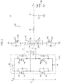
- FIG. 2 Illustrated in detail in Figure 2 is an architecture of an example of the converter apparatus 10, of an insulated bi-directional switching type.
- a converter with the features of the preamble of claim 1 is disclosed e.g. in document US 5,255,174 A .
- designated by the reference 11 is a transformer with a ratio of turns, or transformation ratio, k between the primary and the secondary windings greater than one.
- Said transformer 11 hence comprises a primary winding, designated by the reference 12, whereas designated by the reference 13 is a secondary winding.
- the secondary winding 13 is of the centre-tap type with double winding, i.e., respectively two half-windings 13a and 13b that depart from a centre tap 13c, which constitutes a common terminal.
- Designated by 14 is a battery, which applies a battery voltage V LV to be converted, which is brought back, through an energy-storage reactive circuit, here obtained via a series inductor 15, to the centre tap 13c of the secondary winding 13 of the transformer 11.
- the two half-windings 13a and 13b of the secondary 13 that depart from the centre tap 13c are connected via the other terminals thereof to a ground reference 16 via respective main switches M1 and M2, which identify a switching network for the low voltage, i.e., for carrying out boost conversion.
- Said first main switch M2 and said second main switch M1 are obtained via transistors, in particular MOSFETs, driven by a controller module, not illustrated in Figure 1 , which sends respective driving signals, V1 and V2, in particular voltage levels, on their control electrode, for example, the gate of the MOSFET, to cause opening and closing thereof.
- the converter apparatus 10 can thus operate as a switching insulated DC-DC boost converter, with operation of the main switches M1, M2 of a push-pull type.
- an H-bridge 20 comprising a first pair of MOSFETs MA, MC, connected between the input voltage and the ground reference 16, which form a first leg of the H-bridge 20 and are connected to the positive terminal of the primary 12 via their common (source) terminal.
- the H-bridge 20 moreover comprises further MOSFETs MB and MD, which form the second leg of the bridge 20 and are connected to the negative terminal of the primary 12 via their common node.
- the DC-link capacitance C L can be discharged with a driving of a buck type until the high voltage V HV on the capacitor C L reaches the value V LV of the battery 14 multiplied by the ratio of turns k of the transformer 11.
- the primary voltage V p is brought back onto the secondary winding 13 divided by the ratio of turns k, and corresponds in this case to the voltage V s1 on the half-winding 13b connected to the switch M2.
- the passage of the energy of the capacitor C L to the inductance 15 and to an output node 17 of the converter to which an output capacitor C o is connected and on which the battery 14 can be connected, as illustrated in Figure 1 occurs with the conduction of the MOSFET switch M1 or only of the body diode of the MOSFET switch M1.
- the inductance 15 is recharged via the voltage V s2 on the other half-winding 13a via the main MOSFET switch M2; discharging thereof will occur in a way similar to what has been described above.
- the energy stored by the DC-link capacitance C L is hence transferred directly via the transformer 11 to the inductance 15 and to the battery 14.
- Illustrated in Figure 3 are the time plots of the pairs of driving voltages VA, VD and VB, VC, corresponding to the transistors MA, MD and MB, MC on the two diagonals of the bridge 20, the voltage on the primary winding V P , and the current I L in the inductor 15. Said plots are obtained from driving of a buck type. Likewise represented are the currents I 1 and I 2 that flow in the main MOSFETs M1 and M2.
- the discharge of the DC-link capacitance C L could thus proceed in a dissipative way, for example, exploiting the parasitic resistances of the bridge and/or of the transformer, or else short-circuiting the legs of the bridge, or yet again via driving of one of the semiconductor devices in linear regime.
- said type of circuit presents the drawback of not enabling complete use of a driving of a buck type for discharging the capacitor, it being necessary to resort to dissipative methods when the voltage on the capacitor drops below the level of the battery voltage multiplied by the ratio of turns.
- Document US 3 388 311 A discloses a converter operating as buck converter, which is configured in a way that avoids using a transistor in series on the winding.
- An inductor is provided to store the excess voltage energy.
- the converter includes also circuit paths which can be selectively activated in order to make the current flow in opposite directions in the primary winding of the circuit.
- the European patent application EP 567 108 A1 discloses a control circuit for a discharge lamp in which, on the input stage, it is provided a H bridge of switches connected to the lamp that is driven with a 50% duty cycle to transfer the power to the lamp.
- EP 2 338 903 A1 is an European patent application, in the name of the Applicant, published after the priority date of the outstanding application, therefore prior art under art. 54(3) EPC, that discloses a circuit for the limitation of the in-rush current.
- the object of the present invention is to provide a process solution for discharging a DC-link capacitance in a DC-DC converter apparatus that will overcome the drawbacks of the known art, and, in particular, will enable discharge of the DC-link capacitance to be carried out, avoiding the need to resort to dissipative methods when the voltage on the DC-link capacitance drops below the battery voltage multiplied by the ratio of turns.
- the above object is achieved thanks to a discharging method, as well as a corresponding converter apparatus, which present the characteristics recalled specifically in the ensuing claims.
- the discharging method envisages using a converter apparatus comprising a respective additional switch for discharging the DC-link capacitance in addition to the main switches of the switching network of the DC-DC converter.
- a converter apparatus comprising a respective additional switch for discharging the DC-link capacitance in addition to the main switches of the switching network of the DC-DC converter.
- This driving in boost mode is obtained by exploiting driving of the additional switches for charging the inductance to the voltage value brought back onto the secondary and driving of the main switches for discharging the reactive circuit to the voltage present on one or the other secondary half-winding of the transformer and thus determine an alternative electrical path for the flow of the current through an additional switch and the corresponding half-winding towards the node to which the battery is connected in order to carry out a complete discharge of said DC-link capacitance.
- Figure 4 hence illustrates a converter apparatus suited to implementing the discharging method according to the invention.
- Said circuit designated by the reference 30, corresponds substantially to the circuit of Figure 1 ; however, it comprises the additional switches M3 and M4.
- each of the half-windings 13a and 13b that depart from the centre tap 13c of the secondary 13 and go to one and the other terminal of the secondary is both:
- the additional switch M4 connects the half-winding 13a to the node 17 to which the battery 14 is connected, in parallel to the inductor 15.
- the additional switch M3 connects the half-winding 13b to the node 17 to which the battery 14 is connected, in parallel to the inductor 15.
- a series diode D1 which enables flow of the current to said half-winding 13b and blocks the current to the battery 14.
- Set between the half-winding 13a and the additional switch M4 is a series diode D2, which enables flow of the current to said half-winding 13a and blocks the current to the battery 14.
- Said series diodes D1 and D2 prevent - with the additional MOSFETs M3 and M4 alone on the respective branches, in the buck mode, - the respective body diodes from possibly short-circuiting the drain electrodes of the main MOSFET switches M1 and M2 on the battery 14.
- Illustrated in Figure 5 are diagrams representing the time plots of the signals in the converter apparatus 30 of Figure 4 , in particular the time plots of the pairs of driving voltages VA, VD and VB, VC, corresponding to the transistors MA, MD and MB, MC on the two diagonals of the bridge 20, and the current I L in the inductor 15.
- the currents I 1 and I 2 that flow in the main MOSFETs M1 and M2 and the currents I 3 and I 4 that flow in the additional MOSFETs M3 and M4.
- Said currents are determined by the states of opening and closing described here and imposed on the driving inputs, or gate electrodes, of the MOSFETs, by corresponding driving signals generated by a controller (not represented in the figures).
- Said apparatus 40 enables complete discharging of the DC-link capacitance C L , thus recovering all the energy stored in the capacitor in so far as, when the voltage on the secondary drops below the battery voltage, the converter apparatus starts to be driven in boost mode exploiting driving of the additional MOSFETs M4 and M3.
- MOSFETs MA, MB, MC, MD on the high-voltage side are always driven in a balanced way, i.e., with a 50% duty cycle or in any case a duty cycle synchronous with the secondary winding and longer than or equal to the latter; consequently
- the additional switch M3 is opened to carry out discharge of the energy stored in the inductor 15 onto the battery 14.
- the main switch M1 corresponding the half-winding 13b is closed to enable flow of the current. Possibly, the current can travel on the body diode of the main MOSFET switch M1, which may not necessarily be closed.
- Modulation of the duty cycle occurs only on the MOSFET switches on the low-voltage side LV by monitoring the peak value of the current I L on the inductance 15. Modulation of the duty cycle can be made, for example, according to the classic "current mode", that is, by monitoring the inductor current via a corresponding sensor and by turning off the additional MOSFETs M3 and M4, respectively, when said current reaches a pre-set threshold.
- Figure 6 illustrates a preferred embodiment of the invention, where for each half-winding 13a, 13b the respective additional switch M3 or M4 is envisaged but which moreover comprises, set between the respective half-winding 13a or 13b and the additional switch M3 or M4, a further switch M5 or M6, which is connected in the circuit in the place of the series diode D1 or D2 of Figure 4 , and also this is preferably obtained through a MOSFET, set in back-to-back configuration with respect to the additional switch M3 or M4, with which it has the source electrode in common.
- the further switch M5 is connected to the additional switch M3, whilst the further switch M6 is connected to the additional switch M4.
- Said circuit performs both the function of discharge of the DC-link capacitance C L and a function of limitation of the in-rush current.
- each of the half-windings 13a and 13b that go from the centre tap 13a of the secondary 13 to one and the other terminal thereof is both:
- driving envisages governing said switches of the low-voltage side LV according to the following steps, to limit the in-rush current:
- the in-rush current is a current that is generated upon turning-on of the converter; consequently, the switches M5 and M6 are used for limiting the in-rush current in a temporal step that in general does not overlap the period in which, instead, it is necessary to carry out discharge of the DC-link capacitor.
- the body diode of the additional MOSFETs M3, M4 performs the function of a series blocking diode, which in the aforesaid prior architecture for limiting the in-rush current had to be purposely inserted, whereas the body diode of the further MOSFETs M5, M6 operates as the series diode D1, D2 that blocks the current in the embodiment of Figure 4 during discharge of the DC-link capacitor.
- the driving signals that determine the current plots of Figure 5 are the same for the switch M5 during the discharging mode; i.e., they are governed in the same way, in opening and closing.
- the gates of the MOSFETs M4, M6 and M3, M5 must, instead, be driven with a modulation scheme different from the one used for the discharging mode.
- Figure 7 represents a diagram similar to that of Figure 1b , which shows how with the circuit of Figure 6 it is possible to work on the entire high-voltage positive range V HV , both in buck mode and in boost mode. Below the threshold V LV *k it is necessary to operate in buck mode to limit the in-rush current (quadrant 150), whereas it is necessary to operate in boost mode to carry out complete discharge of the DC-link capacitor (quadrant 250).
- the proposed solution hence advantageously rules out the need to resort to dissipative methods when the voltage on the DC-link capacitor drops below the battery voltage, since a driving in boost mode is carried out for discharge exploiting driving of the additional switches.
- the architecture proposed is suited to being integrated easily with a converter-apparatus architecture suited to limiting the in-rush current.
- the converter apparatus proposed can be used in an extremely wide range of fields where there is required a DC-DC conversion, for example, in the field of mobile electronic instruments, such as cellphones and laptops.
- the converter apparatus proposed finds particular preferred application in the automotive sector, for example, in the aforesaid electric or hybrid vehicles, with thermal and electric engines, which comprise two electrical networks, namely, an electrical network of a traditional type, for example, for loads such as lights or the electronic control unit for controlling the thermal engine and a high-voltage electrical network for the electric engine.
- the H-bridge of switches of the full-bridge type may also be, according to the applications, a bridge of the half-bridge type, in which some switches are replaced by capacitors.
Landscapes
- Engineering & Computer Science (AREA)
- Power Engineering (AREA)
- Dc-Dc Converters (AREA)
Claims (11)
- Procédé pour décharger un condensateur de liaison CC (CL) dans un appareil convertisseur CC-CC isolé, comprenant :un côté haute tension (HV) comportantun réseau en H (20) de commutateurs (MA, MB, MC, MD) commandés par des tensions de commande (VA, VB, VC, VD) correspondantes, connectés entre un noeud d'entrée (25) sur lequel une tension CC (VHV) est appliquée et un premier enroulement (12) d'un transformateur (11), etun condensateur de liaison CC (CL) connecté en parallèle au noeud d'entrée (25) de l'appareil convertisseur (10 ; 30 ; 50), etun côté basse tension (LV) comportantun deuxième enroulement (13) du transformateur (11) avec un nombre de spires (k) inférieur à celui du premier enroulement (12), avec un point de connexion central (13c) à partir duquel partent un premier demi-enroulement (13a) et un second demi-enroulement (13b),un circuit réactif de stockage d'énergie (15), notamment une inductance connectée en série entre le point de connexion central (13c) et un noeud (17) configuré pour le branchement d'une batterie (14) adaptée pour appliquer une tension de batterie CC (VLV), etun réseau de commutation (M1, M2) pour commuter le premier demi-enroulement (13a) et le second demi-enroulement (13b), comportant des dispositifs principaux de commutation (M1, M2) adaptés pour connecter sélectivement le premier demi-enroulement (13a) et le second demi-enroulement (13b) à une référence de tension fixe (16), notamment une référence de masse,le procédé pour décharger étant caractérisé en ce qu'il comprend les actions de :- effectuer, dans une étape initiale, une conversion de l'énergie du côté haute tension (HV) à un côté basse tension (LV) de l'appareil convertisseur (10 ; 30 ; 50), comprenant moduler les temps de fonctionnement des commutateurs en diagonale (MA, MD ; MB, MC) du pont en H (20) pour transférer la tension (VHV) au noeud d'entrée (25) vers le circuit réactif (15), et- à la suite de l'étape initiale, commander les commutateurs principaux (M1, M2) et les commutateurs supplémentaires (M3, M4) compris dans l'appareil convertisseur (10 ; 30 ; 50) et adaptés pour mettre sélectivement en connexion électrique, par leur état ouvert et leur état fermé, le premier demi-enroulement (13a) et le second demi-enroulement (13b) correspondant du deuxième enroulement (13) du transformateur (11) avec le noeud de sortie (17) - configuré pour le branchement d'une batterie (14) - selon une configuration de branchement qui, dans un premier état de configuration, charge le circuit réactif (15) à la tension (Vs1, Vs2) présente au demi-enroulement (13a, 13b) correspondant et, dans un autre état de configuration, détermine un chemin électrique pour le flux de courant passant par le commutateur principal (M1, M2) et le demi-enroulement (13a, 13b) correspondant dans le noeud (17) configuré pour le branchement d'une batterie (14), afin d'effectuer un déchargement complet du condensateur de liaison CC (CL).
- Procédé selon la revendication 1, caractérisé en ce que l'action, qui suit l'étape initiale, de commander les commutateurs principaux (M1, M2) et les commutateurs supplémentaires (M3, M4) survient, lorsque la valeur de la tension (VHV) au condensateur de liaison CC (CL) tombe en-dessous de la valeur de tension (VLV) de la batterie (14) multipliée par le coefficient de transformation (k) du transformateur (11).
- Procédé selon la revendication 1 ou 2, caractérisé en ce que l'opération de commander les commutateurs principaux (MA, M2) et les commutateurs supplémentaires (M3, M4) comprend :lorsque la tension (VHV) au condensateur de liaison CC (CL) est ramenée au premier demi-enroulement (13a) ou second demi-enroulement (13b), obtenant ainsi une tension correspondante (Vs1, Vs2), fermer le commutateur supplémentaire (M3, M4) connecté au demi-enroulement (13a, 13b) pour recharger le circuit réactif (15) à la tension correspondante (Vs1, Vs2), maintenant ouvert le commutateur principal connecté au demi-enroulement (13a, 13b),ouvrir le commutateur (M3, M4) connecté au demi-enroulement (13a, 13b) pour effectuer le déchargement de l'énergie stockée dans la batterie (14), tout en fermant le commutateur principal (M1, M2) connecté au demi-enroulement (13a, 13b) pour faire couler un courant au noeud (17) configuré pour le branchement d'une batterie (14).
- Procédé selon l'une des revendications précédentes, caractérisé en ce qu'il comprend bloquer (D1, D2 ; M5, M6) le courant qui coule du demi-enroulement (13a, 13b) à la batterie (14) par les commutateurs supplémentaires.
- Procédé selon l'une des revendications précédentes, caractérisé en ce qu'il comprend gérer les états d'ouverture et de fermeture d'autres commutateurs (M5, M6) mis en configuration dos-à-dos par rapport aux commutateurs supplémentaires (M3, M4) pour bloquer (D1, D2) le courant qui coule du demi-enroulement ((13a, 13b) à la batterie (14) par les commutateurs supplémentaires (M3, M4) et pour mettre en oeuvre une fonction pour commander le courant d'enclenchement pendant une étape de mise en marche de l'appareil convertisseur (30).
- Procédé selon l'une des revendications précédentes, caractérisé en ce que l'action, qui suit l'étape initiale, de commander les commutateurs principaux (M1, M2) et les commutateurs supplémentaires (M3, M4) comprend en outre commander les commutateurs (MA, MB, MC, MD) du pont en H (20) selon une commutation équilibrée pour ramener la tension (VHV) au condensateur de liaison CC (CL) alternativement au premier demi-enroulement (13a) ou au second demi-enroulement (13b), la commutation équilibrée comprenant une commutation équilibrée de fermeture des commutateurs (MA, MD) d'une première diagonale du pont (20) pour ramener la tension (VHV) du condensateur de liaison CC (CL) à la tension (Vs1) du second demi-enroulement (13b) et de fermeture des commutateurs (MB, MC) d'une seconde diagonale du pont (20) pour ramener la tension (VHV) du condensateur de liaison CC (CL) à la tension (Vs2) du premier demi-enroulement (13a).
- Appareil convertisseur CC-CC isolé comprenant :un côté haute tension (HV) comportantun réseau en H (20) de commutateurs (MA, MB, MC, MD) commandés par des tensions de commande (VA, VB, VC, VD) correspondantes, connectés entre un noeud d'entrée (25) sur lequel une tension CC (VHV) est appliquée et un premier enroulement (12) d'un transformateur (11), etun condensateur de liaison CC (CL) connecté en parallèle au noeud d'entrée (25) de l'appareil convertisseur (10 ; 30 ; 50), etun côté basse tension (LV) comportantun deuxième enroulement (13) du transformateur (11) avec un nombre de spires (k) inférieur à celui du premier enroulement (12), avec un point de connexion central (13c) à partir duquel partent un premier demi-enroulement (13a) et un second demi-enroulement (13b),un circuit réactif de stockage d'énergie (15), notamment une inductance connectée en série entre le point de connexion central (13c) et un noeud (17) configuré pour le branchement d'une batterie (14) adaptée pour appliquer une tension de batterie CC (VLV), etun réseau de commutation (M1, M2) pour commuter le premier demi-enroulement (13a) et le second demi-enroulement (13b), comportant des dispositifs principaux de commutation (M1, M2) adaptés pour connecter sélectivement le premier demi-enroulement (13a) et le second demi-enroulement (13b) à une référence de tension fixe (16), notamment une référence de masse,l'appareil étant caractérisé en ce qu'il comprend des commutateurs supplémentaires (M3, M4) adaptés pour mettre sélectivement en connexion électrique, par leur état ouvert et leur état fermé, le premier demi-enroulement (13a) et le second demi-enroulement (13b) correspondant du deuxième enroulement (13) du transformateur (11) avec le noeud de sortie (17) configuré pour le branchement d'une batterie (14),et comprend un circuit de commande configuré pour fournir des signaux de commande au réseau en H (20), au réseau de commutation (M1, M2) et aux commutateurs supplémentaires (M3, M4) pour mettre en oeuvre le procédé selon les revendications 1 à 6.
- Appareil selon la revendication 7, caractérisé en ce qu'il effectue la conversion entre deux réseaux, l'un à une tension plus élevée et l'autre à une tension moindre, d'un véhicule à moteur, notamment dans des réseaux électriques d'un véhicule à motorisation hybride d'entraînement thermique et d'entraînement électrique ou d'un véhicule purement électrique.
- Appareil selon la revendication 7 ou 8, caractérisé en ce que chacun des commutateurs supplémentaires (M3, M4) respectifs est un MOSFET, l'électrode de source duquel étant connectée à un demi-enroulement (13a, 13b) correspondant, et l'électrode de drain duquel étant connectée au noeud de batterie (14).
- Appareil selon l'une des revendications 7 à 9, caractérisé en ce qu'il comprend, intercalée entre chaque demi-enroulement (13a, 13b) et le commutateur supplémentaire (M3, M4) respectif, une diode en série (D1, D2) pour bloquer le courant du demi-enroulement (13a, 13b) à la batterie (14) par les commutateurs supplémentaires (M3, M4).
- Appareil selon la revendication 9, caractérisé en ce qu'il comprend les autres commutateurs MOSFET (M5, M6), mis en une configuration dos-à-dos en mettant en commun l'électrode de source respective, par rapport aux commutateurs supplémentaires MOSFET (M3, M4) pour bloquer le courant qui coule de la batterie (14) au demi-enroulement (13a, 13b) par les commutateurs supplémentaires (M3, M4) pendant une étape de limitation du courant d'enclenchement et pour bloquer le courant qui coule du demi-enroulement (13a, 13b) à la batterie (14) pendant le déchargement du condensateur de liaison CC (CL).
Applications Claiming Priority (1)
| Application Number | Priority Date | Filing Date | Title |
|---|---|---|---|
| IT000862A ITTO20110862A1 (it) | 2011-09-28 | 2011-09-28 | Procedimento di scarica di un condensatore dc-link in un apparato convertitore dc-dc e relativo apparato convertitore dc-dc |
Publications (2)
| Publication Number | Publication Date |
|---|---|
| EP2575246A1 EP2575246A1 (fr) | 2013-04-03 |
| EP2575246B1 true EP2575246B1 (fr) | 2018-09-05 |
Family
ID=44908022
Family Applications (1)
| Application Number | Title | Priority Date | Filing Date |
|---|---|---|---|
| EP12185612.4A Active EP2575246B1 (fr) | 2011-09-28 | 2012-09-24 | Procédé pour décharger un condensateur de liaison CC dans un appareil convertisseur CC-CC et dispositif convertisseur CC-CC correspondant |
Country Status (2)
| Country | Link |
|---|---|
| EP (1) | EP2575246B1 (fr) |
| IT (1) | ITTO20110862A1 (fr) |
Families Citing this family (1)
| Publication number | Priority date | Publication date | Assignee | Title |
|---|---|---|---|---|
| DE102019212351A1 (de) | 2019-08-19 | 2021-02-25 | Robert Bosch Gmbh | Batteriesystem für ein Kraftfahrzeug, Verfahren zum Betreiben eines Batteriesystems und Kraftfahrzeug |
Citations (1)
| Publication number | Priority date | Publication date | Assignee | Title |
|---|---|---|---|---|
| US5255174A (en) * | 1991-10-18 | 1993-10-19 | Allied-Signal Inc. | Regulated bi-directional DC-to-DC voltage converter which maintains a continuous input current during step-up conversion |
Family Cites Families (3)
| Publication number | Priority date | Publication date | Assignee | Title |
|---|---|---|---|---|
| US3388311A (en) * | 1966-05-27 | 1968-06-11 | Sbd Systems Inc | Power converter for converting an unregulated dc input voltage into a regulated output voltage |
| IT1259553B (it) * | 1992-04-23 | 1996-03-20 | Marelli Autronica | Circuito di comando per una lampada a scarica di gas, particolarmente per l'impiego a bordo di autoveicoli |
| IT1400164B1 (it) * | 2010-05-19 | 2013-05-17 | Torino Politecnico | Apparato convertitore dc-dc con circuito di limitazione della corrente di in-rush e relativo procedimento di conversione dc-dc |
-
2011
- 2011-09-28 IT IT000862A patent/ITTO20110862A1/it unknown
-
2012
- 2012-09-24 EP EP12185612.4A patent/EP2575246B1/fr active Active
Patent Citations (1)
| Publication number | Priority date | Publication date | Assignee | Title |
|---|---|---|---|---|
| US5255174A (en) * | 1991-10-18 | 1993-10-19 | Allied-Signal Inc. | Regulated bi-directional DC-to-DC voltage converter which maintains a continuous input current during step-up conversion |
Also Published As
| Publication number | Publication date |
|---|---|
| EP2575246A1 (fr) | 2013-04-03 |
| ITTO20110862A1 (it) | 2013-03-29 |
Similar Documents
| Publication | Publication Date | Title |
|---|---|---|
| US11772505B2 (en) | System and method for charging using motor driving system | |
| Park et al. | Design and control of a bidirectional resonant dc–dc converter for automotive engine/battery hybrid power generators | |
| US11152852B2 (en) | Bidirectional DC/DC converter and method for charging the intermediate circuit capacitor of a DC/DC converter from the low-voltage battery | |
| US9425641B2 (en) | Battery charging apparatus | |
| US8891254B2 (en) | Power converter and battery charger using the same | |
| US8350523B2 (en) | Charging system with galvanic isolation and multiple operating modes | |
| CN103503292B (zh) | 电力变换装置以及具备该电力变换装置的车载电源装置 | |
| US8487664B2 (en) | System and method for driving a switch | |
| US20120133420A1 (en) | System and Method for Bootstrapping a Switch Driver | |
| US20140268903A1 (en) | System and Method for a Switched-Mode Power Converter | |
| KR101769335B1 (ko) | 멀티 토플러지를 이용한 dc/dc 컨버터 | |
| US9209698B2 (en) | Electric power conversion device | |
| US12512762B2 (en) | Control method for a DC-DC converter and DC-DC converter | |
| US10243455B2 (en) | Bidirectional DC-DC converter | |
| EP2575247B1 (fr) | Procédé pour la conversion CC-CC à modulation par déplacement de phase et appareil de conversion correspondant | |
| WO2013093963A1 (fr) | Appareil de charge | |
| KR101734210B1 (ko) | 양방향 직류-직류 컨버터 | |
| Rathore et al. | A high-gain multilevel dc–dc converter for interfacing electric vehicle battery and inverter | |
| US11496042B2 (en) | Method and device for matching the voltage of the smoothing capacitor of a DC/DC converter before a high-voltage battery is connected | |
| KR20100115087A (ko) | 양방향 dc-dc 컨버터 및 그의 제어방법 | |
| WO2018070496A1 (fr) | Systeme de conversion de puissance | |
| US7116012B2 (en) | Stable power conversion circuits | |
| KR101817903B1 (ko) | 전기 자동차용 고강압 직류/직류 전력변환기 | |
| EP2575246B1 (fr) | Procédé pour décharger un condensateur de liaison CC dans un appareil convertisseur CC-CC et dispositif convertisseur CC-CC correspondant | |
| JP6953634B2 (ja) | Dc/dcコンバータを備える車両充電器 |
Legal Events
| Date | Code | Title | Description |
|---|---|---|---|
| PUAI | Public reference made under article 153(3) epc to a published international application that has entered the european phase |
Free format text: ORIGINAL CODE: 0009012 |
|
| AK | Designated contracting states |
Kind code of ref document: A1 Designated state(s): AL AT BE BG CH CY CZ DE DK EE ES FI FR GB GR HR HU IE IS IT LI LT LU LV MC MK MT NL NO PL PT RO RS SE SI SK SM TR |
|
| AX | Request for extension of the european patent |
Extension state: BA ME |
|
| RAP1 | Party data changed (applicant data changed or rights of an application transferred) |
Owner name: MAGNETI MARELLI S.P.A. |
|
| 17P | Request for examination filed |
Effective date: 20130917 |
|
| RBV | Designated contracting states (corrected) |
Designated state(s): AL AT BE BG CH CY CZ DE DK EE ES FI FR GB GR HR HU IE IS IT LI LT LU LV MC MK MT NL NO PL PT RO RS SE SI SK SM TR |
|
| STAA | Information on the status of an ep patent application or granted ep patent |
Free format text: STATUS: EXAMINATION IS IN PROGRESS |
|
| 17Q | First examination report despatched |
Effective date: 20161124 |
|
| GRAP | Despatch of communication of intention to grant a patent |
Free format text: ORIGINAL CODE: EPIDOSNIGR1 |
|
| STAA | Information on the status of an ep patent application or granted ep patent |
Free format text: STATUS: GRANT OF PATENT IS INTENDED |
|
| RIC1 | Information provided on ipc code assigned before grant |
Ipc: H02M 3/335 20060101AFI20180405BHEP Ipc: H02M 1/00 20060101ALI20180405BHEP |
|
| INTG | Intention to grant announced |
Effective date: 20180426 |
|
| GRAS | Grant fee paid |
Free format text: ORIGINAL CODE: EPIDOSNIGR3 |
|
| GRAA | (expected) grant |
Free format text: ORIGINAL CODE: 0009210 |
|
| STAA | Information on the status of an ep patent application or granted ep patent |
Free format text: STATUS: THE PATENT HAS BEEN GRANTED |
|
| AK | Designated contracting states |
Kind code of ref document: B1 Designated state(s): AL AT BE BG CH CY CZ DE DK EE ES FI FR GB GR HR HU IE IS IT LI LT LU LV MC MK MT NL NO PL PT RO RS SE SI SK SM TR |
|
| REG | Reference to a national code |
Ref country code: GB Ref legal event code: FG4D |
|
| REG | Reference to a national code |
Ref country code: CH Ref legal event code: EP |
|
| REG | Reference to a national code |
Ref country code: AT Ref legal event code: REF Ref document number: 1039006 Country of ref document: AT Kind code of ref document: T Effective date: 20180915 |
|
| REG | Reference to a national code |
Ref country code: DE Ref legal event code: R096 Ref document number: 602012050592 Country of ref document: DE |
|
| REG | Reference to a national code |
Ref country code: IE Ref legal event code: FG4D |
|
| REG | Reference to a national code |
Ref country code: FR Ref legal event code: PLFP Year of fee payment: 7 |
|
| REG | Reference to a national code |
Ref country code: NL Ref legal event code: MP Effective date: 20180905 |
|
| REG | Reference to a national code |
Ref country code: LT Ref legal event code: MG4D |
|
| PG25 | Lapsed in a contracting state [announced via postgrant information from national office to epo] |
Ref country code: BG Free format text: LAPSE BECAUSE OF FAILURE TO SUBMIT A TRANSLATION OF THE DESCRIPTION OR TO PAY THE FEE WITHIN THE PRESCRIBED TIME-LIMIT Effective date: 20181205 Ref country code: RS Free format text: LAPSE BECAUSE OF FAILURE TO SUBMIT A TRANSLATION OF THE DESCRIPTION OR TO PAY THE FEE WITHIN THE PRESCRIBED TIME-LIMIT Effective date: 20180905 Ref country code: GR Free format text: LAPSE BECAUSE OF FAILURE TO SUBMIT A TRANSLATION OF THE DESCRIPTION OR TO PAY THE FEE WITHIN THE PRESCRIBED TIME-LIMIT Effective date: 20181206 Ref country code: NO Free format text: LAPSE BECAUSE OF FAILURE TO SUBMIT A TRANSLATION OF THE DESCRIPTION OR TO PAY THE FEE WITHIN THE PRESCRIBED TIME-LIMIT Effective date: 20181205 Ref country code: FI Free format text: LAPSE BECAUSE OF FAILURE TO SUBMIT A TRANSLATION OF THE DESCRIPTION OR TO PAY THE FEE WITHIN THE PRESCRIBED TIME-LIMIT Effective date: 20180905 Ref country code: LT Free format text: LAPSE BECAUSE OF FAILURE TO SUBMIT A TRANSLATION OF THE DESCRIPTION OR TO PAY THE FEE WITHIN THE PRESCRIBED TIME-LIMIT Effective date: 20180905 Ref country code: SE Free format text: LAPSE BECAUSE OF FAILURE TO SUBMIT A TRANSLATION OF THE DESCRIPTION OR TO PAY THE FEE WITHIN THE PRESCRIBED TIME-LIMIT Effective date: 20180905 |
|
| REG | Reference to a national code |
Ref country code: AT Ref legal event code: MK05 Ref document number: 1039006 Country of ref document: AT Kind code of ref document: T Effective date: 20180905 |
|
| PG25 | Lapsed in a contracting state [announced via postgrant information from national office to epo] |
Ref country code: AL Free format text: LAPSE BECAUSE OF FAILURE TO SUBMIT A TRANSLATION OF THE DESCRIPTION OR TO PAY THE FEE WITHIN THE PRESCRIBED TIME-LIMIT Effective date: 20180905 Ref country code: LV Free format text: LAPSE BECAUSE OF FAILURE TO SUBMIT A TRANSLATION OF THE DESCRIPTION OR TO PAY THE FEE WITHIN THE PRESCRIBED TIME-LIMIT Effective date: 20180905 Ref country code: HR Free format text: LAPSE BECAUSE OF FAILURE TO SUBMIT A TRANSLATION OF THE DESCRIPTION OR TO PAY THE FEE WITHIN THE PRESCRIBED TIME-LIMIT Effective date: 20180905 |
|
| PG25 | Lapsed in a contracting state [announced via postgrant information from national office to epo] |
Ref country code: PL Free format text: LAPSE BECAUSE OF FAILURE TO SUBMIT A TRANSLATION OF THE DESCRIPTION OR TO PAY THE FEE WITHIN THE PRESCRIBED TIME-LIMIT Effective date: 20180905 Ref country code: NL Free format text: LAPSE BECAUSE OF FAILURE TO SUBMIT A TRANSLATION OF THE DESCRIPTION OR TO PAY THE FEE WITHIN THE PRESCRIBED TIME-LIMIT Effective date: 20180905 Ref country code: ES Free format text: LAPSE BECAUSE OF FAILURE TO SUBMIT A TRANSLATION OF THE DESCRIPTION OR TO PAY THE FEE WITHIN THE PRESCRIBED TIME-LIMIT Effective date: 20180905 Ref country code: IS Free format text: LAPSE BECAUSE OF FAILURE TO SUBMIT A TRANSLATION OF THE DESCRIPTION OR TO PAY THE FEE WITHIN THE PRESCRIBED TIME-LIMIT Effective date: 20190105 Ref country code: RO Free format text: LAPSE BECAUSE OF FAILURE TO SUBMIT A TRANSLATION OF THE DESCRIPTION OR TO PAY THE FEE WITHIN THE PRESCRIBED TIME-LIMIT Effective date: 20180905 Ref country code: CZ Free format text: LAPSE BECAUSE OF FAILURE TO SUBMIT A TRANSLATION OF THE DESCRIPTION OR TO PAY THE FEE WITHIN THE PRESCRIBED TIME-LIMIT Effective date: 20180905 Ref country code: AT Free format text: LAPSE BECAUSE OF FAILURE TO SUBMIT A TRANSLATION OF THE DESCRIPTION OR TO PAY THE FEE WITHIN THE PRESCRIBED TIME-LIMIT Effective date: 20180905 Ref country code: EE Free format text: LAPSE BECAUSE OF FAILURE TO SUBMIT A TRANSLATION OF THE DESCRIPTION OR TO PAY THE FEE WITHIN THE PRESCRIBED TIME-LIMIT Effective date: 20180905 |
|
| REG | Reference to a national code |
Ref country code: CH Ref legal event code: PL |
|
| PG25 | Lapsed in a contracting state [announced via postgrant information from national office to epo] |
Ref country code: SK Free format text: LAPSE BECAUSE OF FAILURE TO SUBMIT A TRANSLATION OF THE DESCRIPTION OR TO PAY THE FEE WITHIN THE PRESCRIBED TIME-LIMIT Effective date: 20180905 Ref country code: SM Free format text: LAPSE BECAUSE OF FAILURE TO SUBMIT A TRANSLATION OF THE DESCRIPTION OR TO PAY THE FEE WITHIN THE PRESCRIBED TIME-LIMIT Effective date: 20180905 Ref country code: PT Free format text: LAPSE BECAUSE OF FAILURE TO SUBMIT A TRANSLATION OF THE DESCRIPTION OR TO PAY THE FEE WITHIN THE PRESCRIBED TIME-LIMIT Effective date: 20190105 |
|
| REG | Reference to a national code |
Ref country code: DE Ref legal event code: R097 Ref document number: 602012050592 Country of ref document: DE |
|
| REG | Reference to a national code |
Ref country code: BE Ref legal event code: MM Effective date: 20180930 |
|
| REG | Reference to a national code |
Ref country code: IE Ref legal event code: MM4A |
|
| PG25 | Lapsed in a contracting state [announced via postgrant information from national office to epo] |
Ref country code: LU Free format text: LAPSE BECAUSE OF NON-PAYMENT OF DUE FEES Effective date: 20180924 |
|
| PLBE | No opposition filed within time limit |
Free format text: ORIGINAL CODE: 0009261 |
|
| STAA | Information on the status of an ep patent application or granted ep patent |
Free format text: STATUS: NO OPPOSITION FILED WITHIN TIME LIMIT |
|
| PG25 | Lapsed in a contracting state [announced via postgrant information from national office to epo] |
Ref country code: DK Free format text: LAPSE BECAUSE OF FAILURE TO SUBMIT A TRANSLATION OF THE DESCRIPTION OR TO PAY THE FEE WITHIN THE PRESCRIBED TIME-LIMIT Effective date: 20180905 Ref country code: MC Free format text: LAPSE BECAUSE OF FAILURE TO SUBMIT A TRANSLATION OF THE DESCRIPTION OR TO PAY THE FEE WITHIN THE PRESCRIBED TIME-LIMIT Effective date: 20180905 Ref country code: IE Free format text: LAPSE BECAUSE OF NON-PAYMENT OF DUE FEES Effective date: 20180924 |
|
| 26N | No opposition filed |
Effective date: 20190606 |
|
| GBPC | Gb: european patent ceased through non-payment of renewal fee |
Effective date: 20181205 |
|
| PG25 | Lapsed in a contracting state [announced via postgrant information from national office to epo] |
Ref country code: SI Free format text: LAPSE BECAUSE OF FAILURE TO SUBMIT A TRANSLATION OF THE DESCRIPTION OR TO PAY THE FEE WITHIN THE PRESCRIBED TIME-LIMIT Effective date: 20180905 Ref country code: BE Free format text: LAPSE BECAUSE OF NON-PAYMENT OF DUE FEES Effective date: 20180930 Ref country code: LI Free format text: LAPSE BECAUSE OF NON-PAYMENT OF DUE FEES Effective date: 20180930 Ref country code: CH Free format text: LAPSE BECAUSE OF NON-PAYMENT OF DUE FEES Effective date: 20180930 |
|
| PG25 | Lapsed in a contracting state [announced via postgrant information from national office to epo] |
Ref country code: GB Free format text: LAPSE BECAUSE OF NON-PAYMENT OF DUE FEES Effective date: 20181205 |
|
| PG25 | Lapsed in a contracting state [announced via postgrant information from national office to epo] |
Ref country code: MT Free format text: LAPSE BECAUSE OF NON-PAYMENT OF DUE FEES Effective date: 20180924 |
|
| PG25 | Lapsed in a contracting state [announced via postgrant information from national office to epo] |
Ref country code: HU Free format text: LAPSE BECAUSE OF FAILURE TO SUBMIT A TRANSLATION OF THE DESCRIPTION OR TO PAY THE FEE WITHIN THE PRESCRIBED TIME-LIMIT; INVALID AB INITIO Effective date: 20120924 |
|
| PG25 | Lapsed in a contracting state [announced via postgrant information from national office to epo] |
Ref country code: MK Free format text: LAPSE BECAUSE OF NON-PAYMENT OF DUE FEES Effective date: 20180905 Ref country code: CY Free format text: LAPSE BECAUSE OF FAILURE TO SUBMIT A TRANSLATION OF THE DESCRIPTION OR TO PAY THE FEE WITHIN THE PRESCRIBED TIME-LIMIT Effective date: 20180905 |
|
| PGFP | Annual fee paid to national office [announced via postgrant information from national office to epo] |
Ref country code: TR Payment date: 20220825 Year of fee payment: 11 Ref country code: IT Payment date: 20220825 Year of fee payment: 11 Ref country code: DE Payment date: 20220818 Year of fee payment: 11 |
|
| PGFP | Annual fee paid to national office [announced via postgrant information from national office to epo] |
Ref country code: FR Payment date: 20220819 Year of fee payment: 11 |
|
| REG | Reference to a national code |
Ref country code: DE Ref legal event code: R119 Ref document number: 602012050592 Country of ref document: DE |
|
| PG25 | Lapsed in a contracting state [announced via postgrant information from national office to epo] |
Ref country code: FR Free format text: LAPSE BECAUSE OF NON-PAYMENT OF DUE FEES Effective date: 20230930 Ref country code: DE Free format text: LAPSE BECAUSE OF NON-PAYMENT OF DUE FEES Effective date: 20240403 |
|
| PG25 | Lapsed in a contracting state [announced via postgrant information from national office to epo] |
Ref country code: IT Free format text: LAPSE BECAUSE OF NON-PAYMENT OF DUE FEES Effective date: 20230924 |
|
| PG25 | Lapsed in a contracting state [announced via postgrant information from national office to epo] |
Ref country code: IT Free format text: LAPSE BECAUSE OF NON-PAYMENT OF DUE FEES Effective date: 20230924 |