EP2573821A1 - Thin film solar cell - Google Patents
Thin film solar cell Download PDFInfo
- Publication number
- EP2573821A1 EP2573821A1 EP10851770A EP10851770A EP2573821A1 EP 2573821 A1 EP2573821 A1 EP 2573821A1 EP 10851770 A EP10851770 A EP 10851770A EP 10851770 A EP10851770 A EP 10851770A EP 2573821 A1 EP2573821 A1 EP 2573821A1
- Authority
- EP
- European Patent Office
- Prior art keywords
- electrode layer
- collector
- apertures
- thin film
- insulating substrate
- Prior art date
- Legal status (The legal status is an assumption and is not a legal conclusion. Google has not performed a legal analysis and makes no representation as to the accuracy of the status listed.)
- Withdrawn
Links
Images





Classifications
-
- H—ELECTRICITY
- H10—SEMICONDUCTOR DEVICES; ELECTRIC SOLID-STATE DEVICES NOT OTHERWISE PROVIDED FOR
- H10F—INORGANIC SEMICONDUCTOR DEVICES SENSITIVE TO INFRARED RADIATION, LIGHT, ELECTROMAGNETIC RADIATION OF SHORTER WAVELENGTH OR CORPUSCULAR RADIATION
- H10F19/00—Integrated devices, or assemblies of multiple devices, comprising at least one photovoltaic cell covered by group H10F10/00, e.g. photovoltaic modules
- H10F19/90—Structures for connecting between photovoltaic cells, e.g. interconnections or insulating spacers
- H10F19/902—Structures for connecting between photovoltaic cells, e.g. interconnections or insulating spacers for series or parallel connection of photovoltaic cells
-
- H—ELECTRICITY
- H10—SEMICONDUCTOR DEVICES; ELECTRIC SOLID-STATE DEVICES NOT OTHERWISE PROVIDED FOR
- H10F—INORGANIC SEMICONDUCTOR DEVICES SENSITIVE TO INFRARED RADIATION, LIGHT, ELECTROMAGNETIC RADIATION OF SHORTER WAVELENGTH OR CORPUSCULAR RADIATION
- H10F77/00—Constructional details of devices covered by this subclass
- H10F77/10—Semiconductor bodies
- H10F77/16—Material structures, e.g. crystalline structures, film structures or crystal plane orientations
- H10F77/169—Thin semiconductor films on metallic or insulating substrates
-
- H—ELECTRICITY
- H10—SEMICONDUCTOR DEVICES; ELECTRIC SOLID-STATE DEVICES NOT OTHERWISE PROVIDED FOR
- H10F—INORGANIC SEMICONDUCTOR DEVICES SENSITIVE TO INFRARED RADIATION, LIGHT, ELECTROMAGNETIC RADIATION OF SHORTER WAVELENGTH OR CORPUSCULAR RADIATION
- H10F77/00—Constructional details of devices covered by this subclass
- H10F77/10—Semiconductor bodies
- H10F77/16—Material structures, e.g. crystalline structures, film structures or crystal plane orientations
- H10F77/169—Thin semiconductor films on metallic or insulating substrates
- H10F77/1692—Thin semiconductor films on metallic or insulating substrates the films including only Group IV materials
-
- H—ELECTRICITY
- H10—SEMICONDUCTOR DEVICES; ELECTRIC SOLID-STATE DEVICES NOT OTHERWISE PROVIDED FOR
- H10F—INORGANIC SEMICONDUCTOR DEVICES SENSITIVE TO INFRARED RADIATION, LIGHT, ELECTROMAGNETIC RADIATION OF SHORTER WAVELENGTH OR CORPUSCULAR RADIATION
- H10F77/00—Constructional details of devices covered by this subclass
- H10F77/10—Semiconductor bodies
- H10F77/16—Material structures, e.g. crystalline structures, film structures or crystal plane orientations
- H10F77/169—Thin semiconductor films on metallic or insulating substrates
- H10F77/1698—Thin semiconductor films on metallic or insulating substrates the metallic or insulating substrates being flexible
-
- H—ELECTRICITY
- H10—SEMICONDUCTOR DEVICES; ELECTRIC SOLID-STATE DEVICES NOT OTHERWISE PROVIDED FOR
- H10F—INORGANIC SEMICONDUCTOR DEVICES SENSITIVE TO INFRARED RADIATION, LIGHT, ELECTROMAGNETIC RADIATION OF SHORTER WAVELENGTH OR CORPUSCULAR RADIATION
- H10F77/00—Constructional details of devices covered by this subclass
- H10F77/20—Electrodes
- H10F77/206—Electrodes for devices having potential barriers
- H10F77/211—Electrodes for devices having potential barriers for photovoltaic cells
-
- H—ELECTRICITY
- H10—SEMICONDUCTOR DEVICES; ELECTRIC SOLID-STATE DEVICES NOT OTHERWISE PROVIDED FOR
- H10F—INORGANIC SEMICONDUCTOR DEVICES SENSITIVE TO INFRARED RADIATION, LIGHT, ELECTROMAGNETIC RADIATION OF SHORTER WAVELENGTH OR CORPUSCULAR RADIATION
- H10F77/00—Constructional details of devices covered by this subclass
- H10F77/93—Interconnections
- H10F77/933—Interconnections for devices having potential barriers
- H10F77/935—Interconnections for devices having potential barriers for photovoltaic devices or modules
- H10F77/937—Busbar structures for modules
-
- Y—GENERAL TAGGING OF NEW TECHNOLOGICAL DEVELOPMENTS; GENERAL TAGGING OF CROSS-SECTIONAL TECHNOLOGIES SPANNING OVER SEVERAL SECTIONS OF THE IPC; TECHNICAL SUBJECTS COVERED BY FORMER USPC CROSS-REFERENCE ART COLLECTIONS [XRACs] AND DIGESTS
- Y02—TECHNOLOGIES OR APPLICATIONS FOR MITIGATION OR ADAPTATION AGAINST CLIMATE CHANGE
- Y02E—REDUCTION OF GREENHOUSE GAS [GHG] EMISSIONS, RELATED TO ENERGY GENERATION, TRANSMISSION OR DISTRIBUTION
- Y02E10/00—Energy generation through renewable energy sources
- Y02E10/50—Photovoltaic [PV] energy
Definitions
- the present invention relates to a photovoltaic configured to generate electric power by utilizing solar light, and more particularly to a thin film photovoltaic having a structure in which a plurality of unit photovoltaic cells (unit cells) are connected in series.
- a photovoltaic having a photoelectric conversion layer comprising amorphous silicon, microcrystalline silicon, a compound such as CdTe (cadmium telluride) or CIGS (copper-indium-gallium-selenium), or an organic material because such a photoelectric conversion layer can be formed of a thin film having a thickness of the order of several hundred nm to several ⁇ m and, hence, the photovoltaic can substantially reduce the amount of material to be used therein as compared to a conventional photovoltaic.
- a photovoltaic is called a "thin film photovoltaic".
- One advantage of the thin film photovoltaic is that the thin film photovoltaic can be formed on various types of substrates unlike a conventional crystalline silicon photovoltaic.
- Patent Document 1 describes a thin film photovoltaic having a structure constructed by forming a plurality of unit cells on a sheet (film) substrate and connecting the unit cells in series by utilizing collector apertures and connection apertures which extend through the sheet (film) substrate.
- SCAF Series-Connection through Apertures formed on Film
- FIG. 10 is a plan view illustrating a conventional thin film photovoltaic having the SCAF structure
- FIG. 11 is a sectional view (corresponding to a sectional view taken on line Y-Y of FIG. 10 ) illustrating a method of fabricating the conventional thin film photovoltaic having the SCAF structure step by step.
- electrode layers which assume the same potential when the thin film photovoltaic generates electric power by irradiation with light are given the same hatching. As shown in FIGS.
- the thin film photovoltaic 70 includes an insulating substrate 71 having a front side on which a photoelectric conversion section 75 is formed by stacking a first electrode layer 72, a photoelectric conversion layer 73 and a second electrode layer 74 sequentially and a reverse side on which a back electrode layer 78 is formed by stacking a third electrode layer 76 and a fourth electrode layer 77 sequentially.
- the first electrode layer 72 and the photoelectric conversion layer 73 are stacked over the same region on the front side of the insulating substrate 71, while the third electrode layer 76 and the fourth electrode layer 77 stacked over the same region on the reverse side of the insulating substrate 71.
- transversely opposite end regions on the front side of the insulating film 71 are each formed with a portion comprising a double-layered structure having the first electrode layer 72 and the photoelectric conversion layer 73, while the central region exclusive of the double-layered structure portions is wholly formed with the photoelectric conversion section 75 comprising a triple-layered structure having the first electrode layer 72, photoelectric conversion layer 73 and second electrode layer 74 by stacking the second electrode layer 74 over the photoelectric conversion layer 73.
- the stacks of layers on the front and reverse sides of the insulating substrate 71 are each divided into plural segments by being removed linearly, to form a plurality of unit cells (UC) on the insulating substrate 71 each having the photoelectric conversion section 75 and the back electrode layer 78.
- UC unit cells
- the second electrode layer 74 and the back electrode 78 are electrically connected to each other through collector apertures 79.
- one unit cell (UC n ) has an extension of the first electrode layer 72 electrically connected to an extension of the back electrode layer 78 of the other unit cell (UC n+1 ) through a connection aperture 80.
- connection apertures 80 are formed at plural predetermined locations on the insulating substrate 71.
- Examples of usable materials for the insulating substrate 71 include polyimide films, polyethylene naphthalate (PEN) films, polyethersulfone films (PES), polyethylene terephthalate (PET) films, and aramid films.
- PEN polyethylene naphthalate
- PES polyethersulfone films
- PET polyethylene terephthalate
- aramid films aramid films.
- Each of the connection apertures 80 is shaped circular having a diameter of the order of 1 mm.
- the connection apertures 80 can be formed by mechanical means such as a punch.
- the first electrode layer 72 is formed on the front side of the insulating substrate 71, followed by formation of the third electrode layer 76 on the reverse side of the insulating substrate 71. At that time, the first electrode layer 72 and the third electrode layer 76 overlap each other on the inner periphery of each connection aperture 80 to provide electrical continuity therebetween. Subsequently, as shown in FIG. 11 (c) , a plurality of collector apertures 79 are formed on the insulating substrate 71. Like the connection apertures 80, the collector apertures 79 are each shaped circular having a diameter of the order of 1 mm and can be formed by mechanical means such as a punch.
- the photoelectric conversion layer 73 is formed over the first electrode layer 72.
- the photoelectric conversion layer 73 is a thin film semiconductor layer which can be formed of an amorphous silicon (a-Si) film for example.
- the second electrode layer 74 is formed over the photoelectric conversion layer 73.
- the second electrode layer 74 is a transparent electrode layer which can be formed of an indium tin oxide (ITO) film for example.
- ITO indium tin oxide
- the fourth electrode layer 77 is formed over the third electrode layer 76 formed on the reverse side of the insulating substrate 71.
- the fourth electrode layer 77 is an electrically conductive layer of low resistance which can be formed of a metal film for example.
- the second electrode layer 74 and the fourth electrode layer 77 overlap each other on the inner periphery of each collector aperture 79 to provide electrical continuity therebetween.
- the photoelectric conversion section 75 comprising a stack of the first electrode layer 72, photoelectric conversion layer 73 and second electrode layer 74 is formed on the front side of the insulating substrate 71, while the back electrode layer 78 comprising a stack of the third electrode layer 76 and fourth electrode layer 77 is formed on the reverse side of the insulating substrate 71.
- the stack of layers on the front side of the insulating substrate 71 is removed linearly to form a first line-like removed portion 81, while the stack of layers on the reverse side of the insulating substrate 71 is removed linearly to form a second line-like removed portion 82.
- the plurality of unit cells (UC) each having the photoelectric conversion section 75 stacked on the front side of the insulating substrate 71 and the back electrode layer 78 stacked on the reverse side of the insulating substrate 71 are formed on the insulating substrate 71.
- the second electrode layer 74 and the fourth electrode layer 77 (i.e., back electrode layer 78) in each unit cell (UC) are electrically connected to each other through the collector apertures 79, while the first electrode layer 72 of one unit cell (UC n ) of two adjacent unit cells (UC n and UC n+1 ) has the extension electrically connected to the extension of the third electrode layer 76 (i.e., back electrode layer 78) of the other unit cell (UC n+1 ) through the connection apertures 80.
- the photoelectric conversion layer 73 can be regarded virtually as an insulating layer, the first electrode layer 72 and the second electrode layer 74 are insulated from each other virtually.
- the carriers having traveled to the reverse side of the insulating substrate 71 travel directly to each connection aperture 80.
- the second electrode layer 74 is absent in the regions in which the connection apertures 80 are formed and, hence, the first electrode layer 72 and the third electrode layer 76 (i.e. back electrode layer 78) have electrical continuity therebetween through the inner periphery of each connection hole 80. Therefore, the carriers travel to reach the front side of the insulating substrate 71 again through the connection apertures 80. Thereafter, the carriers travel on the front side of the insulating substrate 71 toward the photoelectric conversion layer 73 of an adjacent unit cell (UC).
- the conventional thin film photovoltaic 70 having the SCAF structure has a structure in which the plurality of unit cells (UCs) are connected in series through the collector apertures 79 and the connection apertures 80.
- Patent Document 1 Japanese Patent Application Laid-open No. H10-233517
- each of the unit cells has the second electrode layer as the transparent electrode layer and the back electrode layer which are electrically connected to each other through the collector apertures and, hence, a power loss (i.e., collection loss) at the transparent electrode layer of high resistance is reduced to a certain extent.
- an object of the present invention is to provide a thin film photovoltaic having a structure including a plurality of unit photovoltaic cells connected in series which allows the conversion efficiency thereof to be improved as compared to the conventional thin film photovoltaic by optimizing the placement of the collector apertures.
- a thin film photovoltaic includes a plurality of unit photovoltaic cells each having a photoelectric conversion section in which a first electrode layer, a photoelectric conversion layer and a transparent second electrode layer are stacked sequentially on a front side of an insulating substrate, and a back electrode layer stacked on a reverse side of the insulating substrate, the unit photovoltaic cells being arranged in such a manner that two adjacent unit photovoltaic cells define therebetween a first overlap region in which a portion of the first electrode layer which fails to form the photoelectric conversion section of one of the two adjacent unit photovoltaic cells and a portion of the back electrode layer of the other unit photovoltaic are opposed to each other across the insulating substrate, and the plurality of unit photovoltaic cells being connected in series by an arrangement such that in each of the unit photovoltaic cells, the second electrode layer and the back electrode layer are electrically connected to each other through a plurality of collector apertures extending through the insulating substrate while the first electrode layer of
- the thin film photovoltaic according to the present invention allows output characteristics (conversion efficiency) thereof to be improved by optimizing the collector aperture placement.
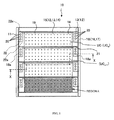
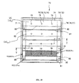
- FIG. 1 is a plan view schematically illustrating the configuration of a thin film photovoltaic 10 according to one embodiment of the present invention
- FIG. 2 is a sectional view taken on line X-X of FIG. 1
- the thin film photovoltaic 10 according to the present embodiment is of the SCAF structure and has basically the same configuration as the conventional thin film photovoltaic 70 shown in FIGS. 10 and 11 .
- the thin film photovoltaic 10 includes a flexible insulating substrate 11.
- the insulating substrate 11 has a front side on which a photoelectric conversion section 15 is formed by stacking a first electrode layer 12, a photoelectric conversion layer 13 and a second electrode layer 14 sequentially and a reverse side on which a back electrode layer 18 is formed by stacking a third electrode layer 16 and a fourth electrode layer 17 sequentially.
- the stacks of layers on the front and reverse sides of the insulating substrate 11 are each divided into plural segments by being removed linearly by a laser patterning process for example, to form a plurality of unit photovoltaic cells (unit cells: UC) on the insulating substrate 11, the unit photovoltaic cells each having the photoelectric conversion section 15 stacked on the front side of the insulating substrate 11 and the back electrode layer 18 stacked on the reverse side of the insulating substrate 11.
- unit photovoltaic cells unit cells: UC
- first line-like removed portions 21 and 22 are first line-like removed portions 21, while the portions of the stack of layers on the reverse side of the insulating substrate 11 which are removed linearly (depicted by broken line) are second line-like removed portions 22.
- the shapes of the first and second line-like removed portions 21 and 22 will be described later.
- the second electrode layer 14 and the fourth electrode layer 17 are electrically connected to each other through a plurality of collector apertures 19.
- the first electrode layer 12 of one unit cell (UC n ) of two adjacent unit cells (UC n and UC n+1) has an extension electrically connected to an extension of the third electrode layer 16 of the other unit cell (UC n-+1 ) through connection apertures 20.
- the thin filmphotovoltaic 10 of this arrangement according to the present embodiment also realizes the structure in which the plurality of unit cells (UC) are connected in series.
- the extension of the first electrode layer 12 of each unit cell (UC) is meant by that region of the first electrode layer 12 formed on the front side of the substrate which fails to form the photoelectric conversion section 15 (i.e., the region which fails to form a triple-layered structure), or a portion thereof, while the extension of the third electrode layer 16 of each unit cell (UC) is meant by that region of the third electrode layer 16 formed on the reverse side of the substrate which is exclusive of that region of the third electrode layer 16 which is coincident with the photoelectric conversion section 15 on the front side of the substrate, or a portion thereof.
- the electrical connection between the first electrode layer 12 of one unit cell (UC n ) and the third electrode layer 16 of the other unit cell (UC n+1 ) through the connection apertures 20 can be expressed otherwise as follows.
- the unit cells are arranged in such a manner that two adjacent unit cells define therebetween an overlap region in which a portion of the first electrode layer 12 which fails to form the photoelectric conversion section 15 of one of the two adjacent unit cells and a portion of the third electrode layer 16 of the other unit cell are opposed to each other across the insulating substrate 11 (hereinafter will be referred to as a "first overlap portion") while the first electrode layer 12 of one of the two adjacent unit cells and the third electrode layer 16 of the other unit cell are electrically connected to each other through the connection apertures 20 extending through the insulating substrate 11 in the first overlap region.
- the insulating substrate 11 is a plastic substrate for example.
- examples of usable materials for such a plastic substrate include polyimide films, polyethylene naphthalate (PEN) films, polyethersulfone films (PES), polyethylene terephthalate (PET) films, and aramid films.
- the thickness of the insulating substrate 11 is 50 ⁇ m for example, which is not limited. In cases where the insulating substrate does not need flexibility, use may be made of a glass substrate or the like.
- the first and third electrode layers 12 and 16 are each a layer of silver (Ag) having a thickness of several hundred nm for example, which is formed by a sputtering process. Though not shown, the first electrode layer 12 has a surface which may be imparted with a texture form for increasing the absorption of light at the photoelectric conversion layer 13 by scattering incident light. While the present embodiment uses the silver (Ag) electrode as the first electrode layer 12, there is no limitation to this feature.
- the first electrode layer 12 may comprise a stacked film formed by depositing titanium dioxide (TiO 2 ) , which is resistant to plasma, on the surface of a silver (Ag) electrode, a tin dioxide (SnO 2 ) film, a zinc oxide (ZnO) film, or a like film.
- TiO 2 titanium dioxide
- a material which can be shaped into an optimal texture form may be used to form the first electrode layer 12.
- the photoelectric conversion layer 13 is a thin film semiconductor layer which has a two-layer tandem structure comprising an amorphous silicon (a-Si) layer and an amorphous silicon-germanium (a-SiGe) layer according to the present embodiment.
- a-Si amorphous silicon
- a-SiGe amorphous silicon-germanium
- amorphous silicon carbide a-SiC
- amorphous silicon oxide a-SiO
- amorphous siliconnitride a-SiN
- microcrystalline silicon ⁇ c-Si
- microcrystalline silicon-germanium ⁇ c-SiGe
- microcrystalline silicon carbide ⁇ c-SiC
- microcrystalline silicon oxide ⁇ c-SiO
- microcrystalline silicon nitride ⁇ c-SiN
- Compound materials and organic materials may also be used.
- Each of the layers forming the photoelectric conversion layer 13 can be formed by plasma chemical vapor deposition (plasma CVD), sputtering, vapor deposition, catalytic chemical vapor deposition (Cat-CVD), photochemical vapor deposition (photo CVD), or a like process.
- plasma CVD plasma chemical vapor deposition
- Cat-CVD catalytic chemical vapor deposition
- photo CVD photochemical vapor deposition
- the second electrode layer 14 is a transparent electrode layer for which the present embodiment uses an indium tin oxide (ITO) film deposited by sputtering.
- ITO indium tin oxide
- there is no limitation to such an indium tin oxide film but use may be made of a tin dioxide (SnO 2 ) film, a zinc oxide (ZnO) film, and a like film.
- the fourth electrode layer 17 is a low-resistant conductive film comprising a metal film.
- the present embodiment uses a nickel (Ni) film deposited by sputtering for the fourth electrode layer 17.
- Ni nickel
- the fourth electrode layer 17 may be formed by using a material other than nickel.
- the collector apertures 19 are placed in such a manner as to be distributed over the entire overlap region in which the photoelectric conversion section 15 and the back electrode layer 18 which form each unit cell (UC) are opposed to each other across the insulating substrate 11 (hereinafter will be referred to as a "second overlap region").
- the connection apertures 20 are placed in the above-described first overlap region, and each unit cell (UC) is provided with six connection apertures 20 (three connection apertures on each of the transversely opposite end sides).
- the collector apertures 19 and the connection apertures 20 are formed by mechanical means such as a punch. In the present embodiment, the collector apertures 19 and the connection apertures 20 are both shaped circular.
- collector apertures 19 and connection apertures 20 may be appropriately changed in shape, size and number so as to meet the specifications and the like of the thin film photovoltaic 10.
- the placement of the collector apertures 19 according to the present embodiment i.e., distributed placement
- Amethodof fabricating the thin filmphotovoltaic 10 according to the present embodiment is basically the same as the method of fabricating the conventional thin film photovoltaic shown in FIG. 10 (see FIG. 11 ) and, for this reason, description thereof is omitted.
- Feature A the shapes of the first and second line-like removed portions
- the conventional thin film photovoltaic 70 is formed with the first and second line-like removed portions 81 and 82 extending like straight lines.
- Each of the connection apertures 80 is placed in a region a of regions a and b defined in plan view between each first line-like removed portion 81 and an adjacent second line-like removed portion 82.
- the second electrode layer 74 and the back electrode layer 78 (including the third and fourth electrode layers 76 and 77) provide electrical continuity therebetween through that collector aperture 79 while the first electrode layer 73 and the back electrode layer 78 provide electrical continuity therebetween through the connection aperture 80, so that electrical continuity is provided between the first electrode layer 73 and the second electrode layer 74, thus causing leakage to occur.
- the collector aperture 79 it is necessary for the collector aperture 79 to be placed in the region b which is different from the region a in which the connection aperture 80 is placed.
- the region which allows the collector aperture 79 to be placed in the conventional thin film photovoltaic 70 is limited to a region c in which the region b and a unit photoelectric conversion section 75 overlap each other.
- the distance over which the carriers generated at a part of the photoelectric conversion section 75 in a region other than the region c, that is, a region near the region a have to travel in the second electrode layer 74 of high resistance up to the collector aperture 79, is long enough to cause a large collection loss.
- each second line-like removed portion 22 is formed to have a bend portion 22a as shown in FIG. 1 , though each first line-like removed portion 21 is formed to extend like a straight line as in the conventional thin film photovoltaic.
- each second line-like removed portion 22 according to the present embodiment has a bend structure on each of the transversely opposite sides of FIG. 1 , the bend structure being formed to have two 90° bends. This feature is provided for the purpose of expanding the second overlap region which allows the collector apertures 19 to be placed therein as compared with that of the conventional thin film photovoltaic while securing the first overlap region for placement of the connection apertures 20.
- each second line-like removed portion 22 is bent (to have bend portions 22a) in plan view so as to embrace the region in which the back electrode layer 18 forming each unit cell (UC) and the whole or a major part of the corresponding photoelectric conversion section 15 are opposed to each other across the insulating substrate 11 as well as to secure the first overlap region for placement of connection apertures 20 on each of the transversely opposite sides of FIG. 1 .
- the back electrode layer 18 of each unit cell (UC) has a bend portion defining the first overlap region (i.e., the region for placement of connection apertures 20 therein) on the side near each adjacent unit cell.
- the back electrode 18 partially projects toward the unit cells adjacent thereto to have projecting portions 18a defining the first overlap regions (i.e., the regions for placement of connection apertures 20 therein) on both of the transversely opposite sides of FIG. 1 .
- the second overlap region which allows the collector apertures 19 to be placed therein is a region A of FIG. 1 , namely, the whole or a major part of the photoelectric conversion section 15.
- the thin film photovoltaic 10 makes the region which allows the collector apertures 19 to be placed therein larger than that of the conventional thin film photovoltaic, thus allowing a desired number of collector apertures 19 to be placed at desired locations in each unit photoelectric conversion section (i.e., second electrode layer 14) to meet the photovoltaic fabrication conditions and the like.
- This feature can shorten the distance over which the carriers generated at each unit photoelectric conversion section have to travel in the second electrode layer 74 of high resistance, thereby making it possible to reduce the collection loss.
- each second line-like removed portion 22 is not limited to that in the present embodiment.
- each second line-like removed portion 22 may be bent not at a right angle but in a slanting direction, or may have a curve which may be folded.
- the "bend portion", as used in the present embodiment, is meant to include these shapes as well as the shape described in the present embodiment.
- each first line-like removed portion 21 has a bend portion while each second line-like removed portion 22 formed to extend like a straight line.
- both the first and second line-like removed portions 21 and 22 may have bend portions.
- each unit cell (UC) at least one of the first and second line-like removed portions 21 and 22 is formed to have the bend portion so that the whole or a major part of the photoelectric conversion section 15 serves as the second overlap region which allows the collector apertures 19 to be placed therein.
- at least one of the first electrode layer 12 and the back electrode layer 18 is formed to have a bend portion so that the whole or a major part of the photoelectric conversion section 15 is opposed to (or overlaps) the back electrode 18 across the insulating substrate 11.
- the bend portion is preferably located within a region around the connection apertures 20 in which the second electrode layer 14 is absent.
- the "region in which the second electrode layer 14 is absent" is meant to include the region on the front side of the insulating substrate 11 in which the second electrode layer 14 is not formed and the region on the reverse side of the insulating substrate 11 which is coincident with the former region.
- each first line-like removed portion 21 or that of each second line-like removed portion 22 can be positioned in the region in which the second electrode layer 14 is absent.
- the stacks of layers on the observe and reverse sides of the insulating substrate 11 are removed linearly to form the first and second line-like removed portions 21 and 22, thereby forming the plurality of unit cells (UC) each having the photoelectric conversion section 15 stacked on the front side of the insulating substrate 11 and the back electrode layer 18 stacked on the reverse side of the insulating substrate 11.
- the plurality of unit cells may be formed on the insulating substrate 11 by stacking the layers on the front and reverse sides of the insulating substrate 11 with use of masks. In this case, the regions in which the masks have prevented the layers from being stacked correspond to the first and second line-like removed portions 21 and 22.
- Feature B the distributed placement of collector apertures
- area loss is meant by a decrease in generated current corresponding to a decrease in power generating area which is caused by the presence of the collector apertures (i.e., a decrease corresponding to the total area of the collector apertures).
- collection loss is meant by a power loss which is incurred when the carriers generated at the photoelectric conversion section travel in the second electrode layer (i.e., transparent electrode layer) and/or when the carriers pass through the collector apertures.
- Factors which are considered to exercise particular effects on the collection loss include the placement and size of the collector apertures, the sheet resistance of the second electrode layer, and the like.
- the simulation was carried out using a finite element method. A voltage drop was calculated by analysis of current in each of mesh regions to derive the current-voltage characteristics (IV characteristics) of the thin film photovoltaic.
- the region which allows the collector apertures to be placed therein is the second overlap region in which the photoelectric conversion section and the back electrode layer which form each unit cell are opposed to each other across the insulating substrate and which corresponds to the region A (rectangular region) in FIG. 1 .
- the characteristics were checked under some conditions by using actually fabricated thin film photovoltaics each having the SCAF structure.
- the output powers of thin film photovoltaics were compared to each other by varying the row number of collector apertures while keeping constant the ratio of the total aperture area of the collector apertures to the whole area of a unit photoelectric conversion section (i.e., power generating region) (hereinafter will be referred to as the "aperture ratio").
- the direction along the long side of the region A is referred to as "X-direction", while the direction along the short side of the region A referred to as "Y-direction”.
- the "the row number”, as mentioned above, is equal to the number of collector apertures aligned in the Y-direction.
- the output power difference i.e., the difference in conversion efficiency
- the output powers of the thin film photovoltaics were compared to each other by varying the row number of collector apertures with three aperture ratios (1%, 2% and 4%) used.
- Each of the aperture ratios was realized by adjusting the number of collector apertures while fixing the diameter of each collector aperture to 1 mm.
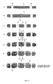
- step (2) the number of collector apertures forming each row is determined.
- the total number of collector apertures is determined in accordance with the aperture ratio and the number of collector apertures forming each row is determined by dividing the total number thus determined by the row number n.
- the total number of collector aperture was adjusted to obtain an integer which is closest to the value calculated.
- step (3) the region A is divided into ⁇ the number of collector apertures forming each row determined in step (2) +1) ⁇ in the X-direction.
- step (4) the collector apertures are placed in such a manner that their respective centers coincide with the points of intersection of the first division lines and the second division lines (i.e., lattice points).
- the collector apertures the number of which realizes a predetermined aperture ratio, are placed in a lattice form in the region A.
- the predetermined number of collector apertures are distributed in the region A, or placed all over the region A, while the plurality of collector apertures thus placed are equally spaced from each other in the X-direction and in the Y-direction. Note that the regions resulting from the division by the steps (1) to (3) are different from mesh regions used in the infinite element method. FIG.
- the positions of all the collector apertures in the X-direction are adjusted so that the distance (L2) in the X-direction from each of the opposite ends of a unit photoelectric conversion section (i.e., power generating region) to those collector apertures which are located most closely thereto is as large as about 1/2 of the distance (L1) in the X-direction between those collector apertures which are located most closely to each other.
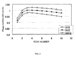
- FIG. 4 illustrates the relationship at an aperture ratio of 2% between the row number of collector apertures and the output power (Pmax) of a thin film photovoltaic calculated.
- the output power (Pmax) of the thin film photovoltaic assumes the highest value at any one of the sheet resistances when the row number of collector apertures is 3 to 4.
- the output power of the thin film photovoltaic lowers as the sheet resistance of the second electrode layer increases.
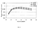
- FIG. 5 illustrates the relationship at an aperture ratio of 4% between the row number of collector apertures and the output power (Pmax) of a thin film photovoltaic calculated.
- the output power (Pmax) assumes the highest value at any one of the sheet resistances when the row number of collector apertures is 5 to 6 and, hence, the row number of collector apertures with which the thin film photovoltaic generates the highest output power (Pmax) is increased as compared with the case of 2% aperture ratio (see FIG. 3 ).
- the range of change in the output power of the thin film photovoltaic with change in the sheet resistance of the second electrode layer is reduced as compared with the case of 2% aperture ratio.
- FIG. 6 illustrates the relationship at an aperture ratio of 1% between the row number of collector apertures and the output power (Pmax) of a thin film photovoltaic calculated.
- the output power (Pmax) assumes the highest value at any one of the sheet resistances when the row number of collector apertures is 2 to 3 and, hence, the row number of collector apertures with which the thin film photovoltaic generates the highest output power (Pmax) is decreased as compared with the case of 2% aperture ratio (see FIG. 4 ).
- the range of change in the output power of the thin film photovoltaic with change in the sheet resistance of the second electrode layer is increased as compared with the case of 2% aperture ratio.
- the optimal row number of collector apertures differs according to the aperture ratio (i.e., the number of collector apertures)
- the plurality of collector apertures are preferably placed in such a manner that the collector apertures are distributed in the overlap region in which the unit photoelectric conversion section and the unit back electrode section which form each unit cell overlap each other while those collector apertures which are located most closely to each other are equally spaced from each other.
- the range of change in the output power of the thin film photovoltaic with change in sheet resistance is considered as follows. As the aperture ratio increases, the number of collector apertures placed in the region A increases and, hence, the spacing between the collector apertures becomes relatively small. This makes the current collecting area per collector aperture decrease, so that the output power of the thin film photovoltaic becomes less susceptible to the sheet resistance of the second electrode layer. Therefore, the range of change in output power with change in the sheet resistance of the second electrode layer decreases with increasing aperture ratio. Within the sheet resistance range from 20 ⁇ to 100 ⁇ , however, the row number of collector apertures with which the thin film photovoltaic generates the highest output power (Pmax) remains substantially the same at each aperture ratio, as can be seen from FIGS. 4 to 6 .
- the plurality of collector apertures are preferably placed in such a manner that the collector apertures are distributed in the overlap region in which the unit photoelectric conversion section and the unit back electrode section which form each unit cell overlap each other while those collector apertures which are located most closely to each other are equally spaced from each other.
- Such a second electrode layer having a sheet resistance ranging from 20 ⁇ to 100 ⁇ is often used in an actual thin film photovoltaic.
- the plurality of collector apertures are placed in such a manner that the collector apertures are distributed in the region A (i.e., the region allowing the collector apertures to be placed therein) while those collector apertures which are located most closely to each other are equally spaced from each other.
- the region A i.e., the region allowing the collector apertures to be placed therein
- those collector apertures which are located most closely to each other are equally spaced from each other.
- the thin film photovoltaic 10 according to the present embodiment which has substantially the same specifications as the thin film photovoltaic subjected to the present study, has an aperture ratio of about 2%.
- the optimal aperture ratio may vary depending on the sheet resistance of the second electrode layer and a like factor. For this reason, it is preferable to establish the aperture ratio after having conducted a study similar to the present study under varied conditions (e.g., in sheet resistance) that are different from those used in the present study.
- FIG. 7 illustrates the relationship between the diameter of each collector aperture and the output power (Pmax) of a thin film photovoltaic.
- the output power (Pmax) of the thin film photovoltaic assumes the highest value when the collector aperture diameter is 1.0 mm.
- the area loss increases as each collector aperture becomes larger, while the resistance at the collector apertures increases as each collector aperture becomes smaller (i.e., as the circumference of each collector aperture becomes shorter). It can be considered from this fact that when the collector aperture diameter is more than 1 mm, the effect of the area loss becomes predominant, which causes the output power (Pmax) to lower, while when the collector aperture diameter is less than 1 mm, the resistance loss at the collector apertures becomes predominant, which causes the output power (Pmax) to lower.
- the output power (Pmax) of the thin film photovoltaic can be said to be sufficiently high (Pmax of not less than 0.99) when the collector aperture diameter falls within the range from 0.6 mm to 1.0 mm.
- the collector aperture diameter is more than 1 mm, on the other hand, the range of change in the output power of the thin film photovoltaic with change in collector aperture diameter becomes larger. Therefore, it is also preferable that the collector aperture diameter is set to fall within the range from 0.6 mm to 1.0 mm (preferably 1.0 mm) for the thin filmphotovoltaic 10 according to the present embodiment which has substantially the same specifications as the thin film photovoltaic subjected to the present study.
- the second electrode layer i.e., transparent electrode layer
- the fourth electrode layer overlap each other on the inner periphery of each collector aperture to provide electrical continuity therebetween. Since the second electrode layer has a high resistance inherently, the sheet resistance of the fourth electrode is considered to be predominant over the resistance change at the collector apertures. Therefore, even when the collector aperture diameter remains the same, the resistance at the collector apertures changes if the material or the thickness of the fourth electrode layer is changed. Though the resistance at the collector apertures (1 mm ⁇ ) was about 0.8 ⁇ according to the present study, it is possible that the optimal collector aperture diameter shifts toward a lower value when the resistance at the collector apertures is decreased by, for example, changing the material for the fourth electrode layer or increasing the film thickness of the fourth electrode layer.
- the optimal collector aperture diameter shifts toward a still lower value because the amount of current collected by each collector aperture decreases as the number of collector apertures increases and, hence, the resistance loss at the collector apertures decreases relatively. Even in such a case, the optimal collector aperture diameter is not considered to become far beyond the above-mentioned range from 0.6 mm to 1 mm. However, a study similar to the present study may be conducted to find out a smaller optimal aperture diameter.
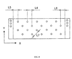
- the collector apertures were arranged in a staggered placement in which the collector apertures forming each even-numbered row (or each odd-numbered row) were displaced in the X-direction in such a manner that each of the collector apertures forming each even-numbered row (or each odd-numbered row) was positioned on the center of gravity of a minimum quadrangle defined by four collector apertures forming part of odd-number rows.
- the positions of all the collector apertures in the X-direction are adjusted so that the distance (L4) in the X-direction between those collector apertures which are located most closely to each other is substantially equal to the distance (L5 or L6) in the X-direction from each of the opposite ends of a unit photoelectric conversion section (i.e., power generating region) to those collector apertures which are located most closely thereto.
- FIG. 9 illustrates the relationship between the row number of collector apertures arranged in a staggered placement and the output power (Pmax) of a thin film photovoltaic.
- FIG. 9 excerpts only the cases where the collector aperture diameter is 1 mm and the sheet resistance of the second electrode layer is 50 ⁇ .
- a preferable placement was such that at least a plurality of collector apertures of a thin film photovoltaic were distributed uniformly in the overlap region in which the unit photoelectric conversion section and the unit back electrode section which formed each unit cell overlapped each other. More specifically, the plurality of collector apertures are placed in a lattice form or a staggered form in such a manner that those collector apertures which are located most closely to each other are equally spaced from each other. Whether in the lattice form or in the staggered form the plurality of collector apertures are to be placed can be appropriately chosen to meet the number of collector apertures or the size and shape of the region allowing the collector apertures to be placed therein.
- the collector apertures are placed in such a manner that the distance from each of the opposite ends of the unit photoelectric conversion section to those collector apertures which are located most closely thereto is equal to or less than the spacing between those collector apertures which are located most closely to each other.
- the optimal row number of collector apertures and the optimal aperture ratio vary with change in the shape or size of the region allowing the collector apertures to be placed therein, it can be considered from the above-described studies that the effect that the conversion efficiency can be improved by the placement in which a plurality of collector apertures are distributed in the second overlap region (i.e., rectangular region A) which allows the collector apertures to be placed therein while those collector apertures which are located most closely to each other are equally spaced from each other, remains the same.
- the change in the shape or size of the region allowing the collector apertures to be placed therein includes not only a simple change in shape or size, but also changes in relation to the connection apertures and their peripheral regions (i.e., mask regions) and changes in the shape of the first line-like removed portions and in the shape of the second line-like removed portions. Since the thin film photovoltaic having the SCAF structure has the region allowing the collector apertures to be placed therein which can be thus changed by the presence of the connection apertures and the presence of the first and second line-like removed portions, an optimal placement of collector apertures has to be determined by simulations conducted taking such conditions into consideration. It is needless to say that the size and number of the connection apertures are preferably established with the area loss incurred by the presence of the connection apertures and the resistance loss at the connection apertures taken into consideration.
Landscapes
- Photovoltaic Devices (AREA)
Abstract
Description
- The present invention relates to a photovoltaic configured to generate electric power by utilizing solar light, and more particularly to a thin film photovoltaic having a structure in which a plurality of unit photovoltaic cells (unit cells) are connected in series.
- In recent years, attention has been focused on photovoltaics as means for solving global environmental problems. Particularly from the viewpoint of reduction in the cost of photovoltaics, attention has been paid to a photovoltaic having a photoelectric conversion layer comprising amorphous silicon, microcrystalline silicon, a compound such as CdTe (cadmium telluride) or CIGS (copper-indium-gallium-selenium), or an organic material because such a photoelectric conversion layer can be formed of a thin film having a thickness of the order of several hundred nm to several µm and, hence, the photovoltaic can substantially reduce the amount of material to be used therein as compared to a conventional photovoltaic. Such a photovoltaic is called a "thin film photovoltaic". One advantage of the thin film photovoltaic is that the thin film photovoltaic can be formed on various types of substrates unlike a conventional crystalline silicon photovoltaic.
- Because the voltage generated by a single photovoltaic is low, it is a general practice to adopt a structure for raising the generated voltage by connecting a plurality of unit photovoltaic cells (unit cells) in series. In the case of the thin film photovoltaic, the series connection structure of unit cells is often realized by forming an electrode layer and a photoelectric conversion layer on a single substrate and dividing the layers thus formed into a plurality of unit cells by laser patterning or the like. For example,
Patent Document 1 describes a thin film photovoltaic having a structure constructed by forming a plurality of unit cells on a sheet (film) substrate and connecting the unit cells in series by utilizing collector apertures and connection apertures which extend through the sheet (film) substrate. Such a photovoltaic structure is called an "SCAF (Series-Connection through Apertures formed on Film) structure". -
FIG. 10 is a plan view illustrating a conventional thin film photovoltaic having the SCAF structure, andFIG. 11 is a sectional view (corresponding to a sectional view taken on line Y-Y ofFIG. 10 ) illustrating a method of fabricating the conventional thin film photovoltaic having the SCAF structure step by step. InFIG. 11 , electrode layers which assume the same potential when the thin film photovoltaic generates electric power by irradiation with light are given the same hatching.
As shown inFIGS. 10 and11 , the thin film photovoltaic 70 includes aninsulating substrate 71 having a front side on which aphotoelectric conversion section 75 is formed by stacking afirst electrode layer 72, aphotoelectric conversion layer 73 and asecond electrode layer 74 sequentially and a reverse side on which aback electrode layer 78 is formed by stacking athird electrode layer 76 and afourth electrode layer 77 sequentially. In this example, thefirst electrode layer 72 and thephotoelectric conversion layer 73 are stacked over the same region on the front side of theinsulating substrate 71, while thethird electrode layer 76 and thefourth electrode layer 77 stacked over the same region on the reverse side of theinsulating substrate 71. InFIG. 10 , transversely opposite end regions on the front side of theinsulating film 71 are each formed with a portion comprising a double-layered structure having thefirst electrode layer 72 and thephotoelectric conversion layer 73, while the central region exclusive of the double-layered structure portions is wholly formed with thephotoelectric conversion section 75 comprising a triple-layered structure having thefirst electrode layer 72,photoelectric conversion layer 73 andsecond electrode layer 74 by stacking thesecond electrode layer 74 over thephotoelectric conversion layer 73.
The stacks of layers on the front and reverse sides of theinsulating substrate 71 are each divided into plural segments by being removed linearly, to form a plurality of unit cells (UC) on theinsulating substrate 71 each having thephotoelectric conversion section 75 and theback electrode layer 78.
In each of the unit cells (UC), thesecond electrode layer 74 and the back electrode 78 (including thethird electrode layer 76 and the fourth electrode layer 77) are electrically connected to each other throughcollector apertures 79. Of two adjacent unit cells (represented by UCn and UC n+1), one unit cell (UCn) has an extension of thefirst electrode layer 72 electrically connected to an extension of theback electrode layer 78 of the other unit cell (UCn+1) through aconnection aperture 80. - With reference to
FIG. 11 , description will be made of a method of fabricating the conventional thin film photovoltaic step by step.
Initially, as shown inFIG. 11(a) , a plurality ofconnection apertures 80 are formed at plural predetermined locations on theinsulating substrate 71. Examples of usable materials for theinsulating substrate 71 include polyimide films, polyethylene naphthalate (PEN) films, polyethersulfone films (PES), polyethylene terephthalate (PET) films, and aramid films. Each of theconnection apertures 80 is shaped circular having a diameter of the order of 1 mm. Theconnection apertures 80 can be formed by mechanical means such as a punch.
Subsequently, as shown inFIG. 11(b) , thefirst electrode layer 72 is formed on the front side of theinsulating substrate 71, followed by formation of thethird electrode layer 76 on the reverse side of theinsulating substrate 71. At that time, thefirst electrode layer 72 and thethird electrode layer 76 overlap each other on the inner periphery of eachconnection aperture 80 to provide electrical continuity therebetween.
Subsequently, as shown inFIG. 11 (c) ,a plurality ofcollector apertures 79 are formed on theinsulating substrate 71. Like theconnection apertures 80, thecollector apertures 79 are each shaped circular having a diameter of the order of 1 mm and can be formed by mechanical means such as a punch. - Subsequently, as shown in
FIG. 11 (d), thephotoelectric conversion layer 73 is formed over thefirst electrode layer 72. Thephotoelectric conversion layer 73 is a thin film semiconductor layer which can be formed of an amorphous silicon (a-Si) film for example.
Subsequently, as shown inFIG. 11(e) , thesecond electrode layer 74 is formed over thephotoelectric conversion layer 73. Thesecond electrode layer 74 is a transparent electrode layer which can be formed of an indium tin oxide (ITO) film for example. During the formation of thesecond electrode layer 74, the connection apertures 80 and peripheral regions thereof are covered with a mask or the like to prevent thesecond electrode layer 74 from being deposited thereon. - Subsequently, as shown in
FIG. 11(f) , thefourth electrode layer 77 is formed over thethird electrode layer 76 formed on the reverse side of theinsulating substrate 71. Thefourth electrode layer 77 is an electrically conductive layer of low resistance which can be formed of a metal film for example. At that time, thesecond electrode layer 74 and thefourth electrode layer 77 overlap each other on the inner periphery of eachcollector aperture 79 to provide electrical continuity therebetween.
By the process steps described above, thephotoelectric conversion section 75 comprising a stack of thefirst electrode layer 72,photoelectric conversion layer 73 andsecond electrode layer 74 is formed on the front side of theinsulating substrate 71, while theback electrode layer 78 comprising a stack of thethird electrode layer 76 andfourth electrode layer 77 is formed on the reverse side of theinsulating substrate 71. - Subsequently, as shown in
FIG. 11(g) , the stack of layers on the front side of theinsulating substrate 71 is removed linearly to form a first line-like removedportion 81, while the stack of layers on the reverse side of theinsulating substrate 71 is removed linearly to form a second line-like removedportion 82. In this way, the plurality of unit cells (UC) each having thephotoelectric conversion section 75 stacked on the front side of theinsulating substrate 71 and theback electrode layer 78 stacked on the reverse side of theinsulating substrate 71 are formed on theinsulating substrate 71. As described above, thesecond electrode layer 74 and the fourth electrode layer 77 (i.e., back electrode layer 78) in each unit cell (UC) are electrically connected to each other through thecollector apertures 79, while thefirst electrode layer 72 of one unit cell (UCn) of two adjacent unit cells (UCn and UC n+1) has the extension electrically connected to the extension of the third electrode layer 76 (i.e., back electrode layer 78) of the other unit cell (UCn+1) through theconnection apertures 80. - When carriers (electrons and positive holes) are generated in the
photoelectric conversion layer 73 of each unit cell (UC) by irradiation of the thin film photovoltaic 70 with light, an electric field in the pn junction causes carriers of one type to flow toward the second electrode layer (i.e., transparent electrode layer) 74. Since thesecond electrode layer 74 has electrical continuity with the fourth electrode layer 77 (i.e., back electrode 78) through the inner periphery of eachcollector aperture 79, the carriers having flowed into thesecond electrode layer 74 travel toward the reverse side of theinsulating substrate 71 through thecollector apertures 79. Because thephotoelectric conversion layer 73 can be regarded virtually as an insulating layer, thefirst electrode layer 72 and thesecond electrode layer 74 are insulated from each other virtually. The carriers having traveled to the reverse side of theinsulating substrate 71 travel directly to eachconnection aperture 80. Thesecond electrode layer 74 is absent in the regions in which theconnection apertures 80 are formed and, hence, thefirst electrode layer 72 and the third electrode layer 76 (i.e. back electrode layer 78) have electrical continuity therebetween through the inner periphery of eachconnection hole 80. Therefore, the carriers travel to reach the front side of theinsulating substrate 71 again through theconnection apertures 80. Thereafter, the carriers travel on the front side of theinsulating substrate 71 toward thephotoelectric conversion layer 73 of an adjacent unit cell (UC). Thus, the conventional thin film photovoltaic 70 having the SCAF structure has a structure in which the plurality of unit cells (UCs) are connected in series through thecollector apertures 79 and theconnection apertures 80. - Patent Document 1 : Japanese Patent Application Laid-open No.
H10-233517 - In the conventional thin film photovoltaic described above, each of the unit cells has the second electrode layer as the transparent electrode layer and the back electrode layer which are electrically connected to each other through the collector apertures and, hence, a power loss (i.e., collection loss) at the transparent electrode layer of high resistance is reduced to a certain extent.
- However, absolutely no study has been made on how to place the collector apertures in the above-described conventional thin film photovoltaic. For this reason, the distance over which the carriers generated in a unit photoelectric conversion section have to travel in the transparent electrode layer of high resistance up to each collector aperture is long enough to leave the collection loss still large. Because the placement of the collector apertures is considered to exercise an effect on the output characteristics of a thin film photovoltaic, it is desired to optimize the placement as far as possible.
- The present invention has been made in view of such challenges. Accordingly, an object of the present invention is to provide a thin film photovoltaic having a structure including a plurality of unit photovoltaic cells connected in series which allows the conversion efficiency thereof to be improved as compared to the conventional thin film photovoltaic by optimizing the placement of the collector apertures.
- A thin film photovoltaic according to one aspect of the present invention includes a plurality of unit photovoltaic cells each having a photoelectric conversion section in which a first electrode layer, a photoelectric conversion layer and a transparent second electrode layer are stacked sequentially on a front side of an insulating substrate, and a back electrode layer stacked on a reverse side of the insulating substrate, the unit photovoltaic cells being arranged in such a manner that two adjacent unit photovoltaic cells define therebetween a first overlap region in which a portion of the first electrode layer which fails to form the photoelectric conversion section of one of the two adjacent unit photovoltaic cells and a portion of the back electrode layer of the other unit photovoltaic are opposed to each other across the insulating substrate, and the plurality of unit photovoltaic cells being connected in series by an arrangement such that in each of the unit photovoltaic cells, the second electrode layer and the back electrode layer are electrically connected to each other through a plurality of collector apertures extending through the insulating substrate while the first electrode layer of one of the two adjacent unit photovoltaic cells and the back electrode layer of the other unit photovoltaic are electrically connected to each other through at least one connection aperture extending through the insulating substrate in the first overlap region, wherein the plurality of collector apertures are placed in such a manner that the collector apertures are distributed in a second overlap region in which the photoelectric conversion section and the back electrode layer which form each of the unit photovoltaic cells are opposed to each other across the insulating substrate while those collector apertures which are placed most closely to each other are equally spaced from each other.
- It was confirmed from a study made by the inventors of the present invention that a thin film photovoltaic having a collector aperture placement in which a plurality of collector apertures are distributed in a target region (i.e., the region which allows the collector apertures to be placed therein) while those collector apertures which are placed most closely to each other are equally spaced from each other generated a higher output power than a thin film photovoltaic having any other collector aperture placement. Therefore, the thin film photovoltaic according to the present invention allows output characteristics (conversion efficiency) thereof to be improved by optimizing the collector aperture placement.
-
-
FIG. 1 is a plan view schematically illustrating the configuration of a thin film photovoltaic according to one embodiment of the present invention; -
FIG. 2 is a sectional view taken on line X-X ofFIG. 1 ; -
FIG. 3 is a view illustrating a placement of collector apertures in a lattice form; -
FIG. 4 is a diagram illustrating the relationship at an aperture ratio of 2% between the row number of collector apertures and the output power (Pmax) of a thin film photovoltaic; -
FIG. 5 is a diagram illustrating the relationship at an aperture ratio of 4% between the row number of collector apertures and the output power (Pmax) of a thin film photovoltaic; -
FIG. 6 is a diagram illustrating the relationship at an aperture ratio of 1% between the row number of collector apertures and the output power (Pmax) of a thin film photovoltaic; -
FIG. 7 is a diagram illustrating the relationship between the collector aperture diameter and the output power (Pmax) of a thin film photovoltaic; -
FIG. 8 is a view schematically illustrating a placement of collector apertures in a staggered form; -
FIG. 9 is a diagram illustrating the relationship between the row number of collector apertures placed in a staggered form and the output power (Pmax) of a thin film photovoltaic; -
FIG. 10 is a plan view of a conventional thin film photovoltaic; and -
FIG. 11 is a view, corresponding to a sectional view taken on line Y-Y ofFIG. 7 , illustrating a method of fabricating the conventional thin film photovoltaic step by step. - Hereinafter, embodiments of the present invention will be described with reference to the attached drawings.
FIG. 1 is a plan view schematically illustrating the configuration of a thin film photovoltaic 10 according to one embodiment of the present invention, andFIG. 2 is a sectional view taken on line X-X ofFIG. 1 . The thin film photovoltaic 10 according to the present embodiment is of the SCAF structure and has basically the same configuration as the conventional thin film photovoltaic 70 shown inFIGS. 10 and11 . In brief, the thin film photovoltaic 10 includes a flexible insulatingsubstrate 11. The insulatingsubstrate 11 has a front side on which aphotoelectric conversion section 15 is formed by stacking afirst electrode layer 12, aphotoelectric conversion layer 13 and asecond electrode layer 14 sequentially and a reverse side on which aback electrode layer 18 is formed by stacking athird electrode layer 16 and afourth electrode layer 17 sequentially. - The stacks of layers on the front and reverse sides of the insulating
substrate 11 are each divided into plural segments by being removed linearly by a laser patterning process for example, to form a plurality of unit photovoltaic cells (unit cells: UC) on the insulatingsubstrate 11, the unit photovoltaic cells each having thephotoelectric conversion section 15 stacked on the front side of the insulatingsubstrate 11 and theback electrode layer 18 stacked on the reverse side of the insulatingsubstrate 11. The portions of the stack of layers on the front side of the insulatingsubstrate 11 which are removed linearly (depicted by solid line) are first line-likeremoved portions 21, while the portions of the stack of layers on the reverse side of the insulatingsubstrate 11 which are removed linearly (depicted by broken line) are second line-likeremoved portions 22. The shapes of the first and second line-likeremoved portions - In each of the unit cells (UC), the
second electrode layer 14 and thefourth electrode layer 17 are electrically connected to each other through a plurality ofcollector apertures 19. Thefirst electrode layer 12 of one unit cell (UCn) of two adjacent unit cells (UCn and UCn+1) has an extension electrically connected to an extension of thethird electrode layer 16 of the other unit cell (UCn-+1) throughconnection apertures 20. Thethin filmphotovoltaic 10 of this arrangement according to the present embodiment also realizes the structure in which the plurality of unit cells (UC) are connected in series. The extension of thefirst electrode layer 12 of each unit cell (UC) is meant by that region of thefirst electrode layer 12 formed on the front side of the substrate which fails to form the photoelectric conversion section 15 (i.e., the region which fails to form a triple-layered structure), or a portion thereof, while the extension of thethird electrode layer 16 of each unit cell (UC) is meant by that region of thethird electrode layer 16 formed on the reverse side of the substrate which is exclusive of that region of thethird electrode layer 16 which is coincident with thephotoelectric conversion section 15 on the front side of the substrate, or a portion thereof.
The electrical connection between thefirst electrode layer 12 of one unit cell (UCn) and thethird electrode layer 16 of the other unit cell (UCn+1) through theconnection apertures 20 can be expressed otherwise as follows.
The unit cells are arranged in such a manner that two adjacent unit cells define therebetween an overlap region in which a portion of thefirst electrode layer 12 which fails to form thephotoelectric conversion section 15 of one of the two adjacent unit cells and a portion of thethird electrode layer 16 of the other unit cell are opposed to each other across the insulating substrate 11 (hereinafter will be referred to as a "first overlap portion") while thefirst electrode layer 12 of one of the two adjacent unit cells and thethird electrode layer 16 of the other unit cell are electrically connected to each other through theconnection apertures 20 extending through the insulatingsubstrate 11 in the first overlap region. - Further description is directed to the components of the above-described thin film photovoltaic 10.
The insulatingsubstrate 11 is a plastic substrate for example. Examples of usable materials for such a plastic substrate include polyimide films, polyethylene naphthalate (PEN) films, polyethersulfone films (PES), polyethylene terephthalate (PET) films, and aramid films. The thickness of the insulatingsubstrate 11 is 50 µm for example, which is not limited. In cases where the insulating substrate does not need flexibility, use may be made of a glass substrate or the like. - The first and third electrode layers 12 and 16 are each a layer of silver (Ag) having a thickness of several hundred nm for example, which is formed by a sputtering process. Though not shown, the
first electrode layer 12 has a surface which may be imparted with a texture form for increasing the absorption of light at thephotoelectric conversion layer 13 by scattering incident light. While the present embodiment uses the silver (Ag) electrode as thefirst electrode layer 12, there is no limitation to this feature. For example, thefirst electrode layer 12 may comprise a stacked film formed by depositing titanium dioxide (TiO2) , which is resistant to plasma, on the surface of a silver (Ag) electrode, a tin dioxide (SnO2) film, a zinc oxide (ZnO) film, or a like film. Alternatively, a material which can be shaped into an optimal texture form may be used to form thefirst electrode layer 12. - The
photoelectric conversion layer 13 is a thin film semiconductor layer which has a two-layer tandem structure comprising an amorphous silicon (a-Si) layer and an amorphous silicon-germanium (a-SiGe) layer according to the present embodiment. However, there is no limitation to this feature. Other usable materials for thephotoelectric conversion layer 13 include amorphous silicon carbide (a-SiC), amorphous silicon oxide (a-SiO), amorphous siliconnitride (a-SiN), microcrystalline silicon (µc-Si), microcrystalline silicon-germanium (µc-SiGe), microcrystalline silicon carbide (µc-SiC), microcrystalline silicon oxide (µc-SiO), microcrystalline silicon nitride (µc-SiN), and a like material. Compound materials and organic materials may also be used. Each of the layers forming thephotoelectric conversion layer 13 can be formed by plasma chemical vapor deposition (plasma CVD), sputtering, vapor deposition, catalytic chemical vapor deposition (Cat-CVD), photochemical vapor deposition (photo CVD), or a like process. - The
second electrode layer 14 is a transparent electrode layer for which the present embodiment uses an indium tin oxide (ITO) film deposited by sputtering. However, there is no limitation to such an indium tin oxide film, but use may be made of a tin dioxide (SnO2) film, a zinc oxide (ZnO) film, and a like film. - The
fourth electrode layer 17 is a low-resistant conductive film comprising a metal film. The present embodiment uses a nickel (Ni) film deposited by sputtering for thefourth electrode layer 17. However, there is no limitation to such a nickel film, but thefourth electrode layer 17 may be formed by using a material other than nickel. - The collector apertures 19 are placed in such a manner as to be distributed over the entire overlap region in which the
photoelectric conversion section 15 and theback electrode layer 18 which form each unit cell (UC) are opposed to each other across the insulating substrate 11 (hereinafter will be referred to as a "second overlap region"). The connection apertures 20 are placed in the above-described first overlap region, and each unit cell (UC) is provided with six connection apertures 20 (three connection apertures on each of the transversely opposite end sides). The collector apertures 19 and theconnection apertures 20 are formed by mechanical means such as a punch. In the present embodiment, thecollector apertures 19 and theconnection apertures 20 are both shaped circular. However, thecollector apertures 19 andconnection apertures 20 may be appropriately changed in shape, size and number so as to meet the specifications and the like of the thin film photovoltaic 10. The placement of thecollector apertures 19 according to the present embodiment (i.e., distributed placement) will be described later.
Amethodof fabricating thethin filmphotovoltaic 10 according to the present embodiment is basically the same as the method of fabricating the conventional thin film photovoltaic shown inFIG. 10 (seeFIG. 11 ) and, for this reason, description thereof is omitted. - Description will be made of some features of the thin film photovoltaic 10 which are characteristic of the present embodiment while making comparison with the conventional thin film photovoltaic (see
FIG. 10 ). Here, description is directed particularly to feature A: the shapes of the first and second line-like removed portions and feature B: the distributed placement of collector apertures. - Feature A: the shapes of the first and second line-like removed portions
As shown inFIG. 10 , the conventional thin film photovoltaic 70 is formed with the first and second line-likeremoved portions connection apertures 80 is placed in a region a of regions a and b defined in plan view between each first line-like removedportion 81 and an adjacent second line-like removedportion 82. If acollector aperture 79 is placed in the region a, thesecond electrode layer 74 and the back electrode layer 78 (including the third and fourth electrode layers 76 and 77) provide electrical continuity therebetween through thatcollector aperture 79 while thefirst electrode layer 73 and theback electrode layer 78 provide electrical continuity therebetween through theconnection aperture 80, so that electrical continuity is provided between thefirst electrode layer 73 and thesecond electrode layer 74, thus causing leakage to occur. For this reason, it is necessary for thecollector aperture 79 to be placed in the region b which is different from the region a in which theconnection aperture 80 is placed. As a result, the region which allows thecollector aperture 79 to be placed in the conventional thin film photovoltaic 70 is limited to a region c in which the region b and a unitphotoelectric conversion section 75 overlap each other. In this case, the distance over which the carriers generated at a part of thephotoelectric conversion section 75 in a region other than the region c, that is, a region near the region a have to travel in thesecond electrode layer 74 of high resistance up to thecollector aperture 79, is long enough to cause a large collection loss. - In the thin film photovoltaic 10 according to the present embodiment, by contrast, each second line-like removed
portion 22 is formed to have abend portion 22a as shown inFIG. 1 , though each first line-like removedportion 21 is formed to extend like a straight line as in the conventional thin film photovoltaic. Specifically, each second line-like removedportion 22 according to the present embodiment has a bend structure on each of the transversely opposite sides ofFIG. 1 , the bend structure being formed to have two 90° bends. This feature is provided for the purpose of expanding the second overlap region which allows thecollector apertures 19 to be placed therein as compared with that of the conventional thin film photovoltaic while securing the first overlap region for placement of theconnection apertures 20. That is, each second line-like removedportion 22 is bent (to havebend portions 22a) in plan view so as to embrace the region in which theback electrode layer 18 forming each unit cell (UC) and the whole or a major part of the correspondingphotoelectric conversion section 15 are opposed to each other across the insulatingsubstrate 11 as well as to secure the first overlap region for placement ofconnection apertures 20 on each of the transversely opposite sides ofFIG. 1 .
Stated otherwise, theback electrode layer 18 of each unit cell (UC) has a bend portion defining the first overlap region (i.e., the region for placement ofconnection apertures 20 therein) on the side near each adjacent unit cell. More specifically, theback electrode 18 partially projects toward the unit cells adjacent thereto to have projectingportions 18a defining the first overlap regions (i.e., the regions for placement ofconnection apertures 20 therein) on both of the transversely opposite sides ofFIG. 1 . In each unit cell (UC), the second overlap region which allows thecollector apertures 19 to be placed therein is a region A ofFIG. 1 , namely, the whole or a major part of thephotoelectric conversion section 15. For this reason, the thin film photovoltaic 10 according to the present embodiment makes the region which allows thecollector apertures 19 to be placed therein larger than that of the conventional thin film photovoltaic, thus allowing a desired number ofcollector apertures 19 to be placed at desired locations in each unit photoelectric conversion section (i.e., second electrode layer 14) to meet the photovoltaic fabrication conditions and the like. This feature can shorten the distance over which the carriers generated at each unit photoelectric conversion section have to travel in thesecond electrode layer 74 of high resistance, thereby making it possible to reduce the collection loss. - The shape of each second line-like removed
portion 22 is not limited to that in the present embodiment. For example, each second line-like removedportion 22 may be bent not at a right angle but in a slanting direction, or may have a curve which may be folded. The "bend portion", as used in the present embodiment, is meant to include these shapes as well as the shape described in the present embodiment. It is also possible that each first line-like removedportion 21 has a bend portion while each second line-like removedportion 22 formed to extend like a straight line. Alternatively, both the first and second line-likeremoved portions
Simply speaking, in each unit cell (UC) at least one of the first and second line-likeremoved portions photoelectric conversion section 15 serves as the second overlap region which allows thecollector apertures 19 to be placed therein. As a result, in each unit cell (UC) at least one of thefirst electrode layer 12 and theback electrode layer 18 is formed to have a bend portion so that the whole or a major part of thephotoelectric conversion section 15 is opposed to (or overlaps) theback electrode 18 across the insulatingsubstrate 11. - When each first line-like removed
portion 21 or each second line-like removedportion 22 has the bend portion, the bend portion is preferably located within a region around theconnection apertures 20 in which thesecond electrode layer 14 is absent. The "region in which thesecond electrode layer 14 is absent", as used herein, is meant to include the region on the front side of the insulatingsubstrate 11 in which thesecond electrode layer 14 is not formed and the region on the reverse side of the insulatingsubstrate 11 which is coincident with the former region. When each first line-like removedportion 21 has the bend portion, the region of concern is the former region, while when each second line-like removedportion 22 has the bend portion, the region of concern is the latter region. By locating the bend portion of each first line-like removedportion 21 or that of each second line-like removedportion 22 in the region in which thesecond electrode layer 14 is absent, the region which allows thecollector apertures 19 to be placed therein (i.e. , the second overlap region) can be expanded. - In the present embodiment, the stacks of layers on the observe and reverse sides of the insulating
substrate 11 are removed linearly to form the first and second line-likeremoved portions photoelectric conversion section 15 stacked on the front side of the insulatingsubstrate 11 and theback electrode layer 18 stacked on the reverse side of the insulatingsubstrate 11. There is no limitation to this feature. For example, the plurality of unit cells may be formed on the insulatingsubstrate 11 by stacking the layers on the front and reverse sides of the insulatingsubstrate 11 with use of masks. In this case, the regions in which the masks have prevented the layers from being stacked correspond to the first and second line-likeremoved portions - Feature B: the distributed placement of collector apertures
In order to study an optimal placement of the collector apertures, a simulation on the output characteristics of a thin film photovoltaic was carried out with an area loss and a collection loss taken into consideration. The "area loss", as used herein, is meant by a decrease in generated current corresponding to a decrease in power generating area which is caused by the presence of the collector apertures (i.e., a decrease corresponding to the total area of the collector apertures). The "collection loss", as used herein, is meant by a power loss which is incurred when the carriers generated at the photoelectric conversion section travel in the second electrode layer (i.e., transparent electrode layer) and/or when the carriers pass through the collector apertures. Factors which are considered to exercise particular effects on the collection loss include the placement and size of the collector apertures, the sheet resistance of the second electrode layer, and the like. The simulation was carried out using a finite element method. A voltage drop was calculated by analysis of current in each of mesh regions to derive the current-voltage characteristics (IV characteristics) of the thin film photovoltaic. The region which allows the collector apertures to be placed therein is the second overlap region in which the photoelectric conversion section and the back electrode layer which form each unit cell are opposed to each other across the insulating substrate and which corresponds to the region A (rectangular region) inFIG. 1 . The characteristics were checked under some conditions by using actually fabricated thin film photovoltaics each having the SCAF structure. - Initially, a study was conducted on the row number of collector apertures placed in the region A.
Specifically, the output powers of thin film photovoltaics were compared to each other by varying the row number of collector apertures while keeping constant the ratio of the total aperture area of the collector apertures to the whole area of a unit photoelectric conversion section (i.e., power generating region) (hereinafter will be referred to as the "aperture ratio"). In the following description, the direction along the long side of the region A is referred to as "X-direction", while the direction along the short side of the region A referred to as "Y-direction". The "the row number", as mentioned above, is equal to the number of collector apertures aligned in the Y-direction. - When the aperture ratio is constant, the area loss remains substantially the same and, therefore, the output power difference (i.e., the difference in conversion efficiency) between the thin film photovoltaics depends on how to place the collector apertures. In the present study, the output powers of the thin film photovoltaics were compared to each other by varying the row number of collector apertures with three aperture ratios (1%, 2% and 4%) used. Each of the aperture ratios was realized by adjusting the number of collector apertures while fixing the diameter of each collector aperture to 1 mm. In the present study, the output powers (Pmax) of the thin film photovoltaics were calculated under the conditions: the size of the region A allowing the collector apertures to be placed therein (rectangular region) = 195.6 mm (X) × 26.8 (Y) mm; and the sheet resistance of the second electrode layer = 20 Q, 50 Ω and 100 Ω for each of the aperture ratios.
- Specifically, a plurality of collector apertures were placed in the region A according to the following process steps (1) to (4) and the output powers (Pmax) of the thin film photovoltaics were calculated with the collector apertures in different placements.
In step (1), the row number n of collector apertures is determined and the region A is divided into (n+1) regions in the Y-direction. For example, when five rows of collector apertures are to be placed, it follows that 26.8/(5+1) = 4.47. Therefore, five division lines in parallel with the long side of the region A (hereinafter will be referred to as "first division lines") are drawn at intervals of 4.47 mm in the Y-direction to divide the region A into six regions. Thus, six rectangular regions each sized 195.6 mm × 4.47 mm are formed in the region A. - In step (2), the number of collector apertures forming each row is determined. Here, the total number of collector apertures is determined in accordance with the aperture ratio and the number of collector apertures forming each row is determined by dividing the total number thus determined by the row number n. For example, when five rows of collector apertures are to be placed with the aperture ratio set to 2%, the 2% aperture ratio corresponds to about 130 collector apertures (1 mmφ) formed in the region A and, hence, the number of collector apertures forming each row is 130/5 = 26. In the present study, when the value obtained by dividing the total number of collector apertures by the row number n was not an integer, the total number of collector aperture was adjusted to obtain an integer which is closest to the value calculated.
- In step (3), the region A is divided into {the number of collector apertures forming each row determined in step (2) +1) } in the X-direction. For example, when five rows of collector apertures are to be placed with the aperture ratio set to 2%, it follows that 195. 6/ (26+1) = 7.24. Therefore, 26 division lines in parallel with the short side of the region A (hereinafter will be referred to as "second division lines") are drawn at intervals of 7.24 mm in the X-direction to divide the region A into 27 regions. As a result, the region A is divided in a lattice form by the first and second division lines to form 162 (= 6 × 27) rectangular regions each sized 7.24 mm × 4.47 mm in the region A.
- In step (4), the collector apertures are placed in such a manner that their respective centers coincide with the points of intersection of the first division lines and the second division lines (i.e., lattice points).
By the steps (1) to (4), the collector apertures, the number of which realizes a predetermined aperture ratio, are placed in a lattice form in the region A. By this placement, the predetermined number of collector apertures are distributed in the region A, or placed all over the region A, while the plurality of collector apertures thus placed are equally spaced from each other in the X-direction and in the Y-direction. Note that the regions resulting from the division by the steps (1) to (3) are different from mesh regions used in the infinite element method.
FIG. 3 is a view schematically illustrating a placement of plural collector apertures in a lattice form (row number = 4). In the lattice-form placement shown inFIG. 3 , the positions of all the collector apertures in the X-direction are adjusted so that the distance (L2) in the X-direction from each of the opposite ends of a unit photoelectric conversion section (i.e., power generating region) to those collector apertures which are located most closely thereto is as large as about 1/2 of the distance (L1) in the X-direction between those collector apertures which are located most closely to each other. -
FIG. 4 illustrates the relationship at an aperture ratio of 2% between the row number of collector apertures and the output power (Pmax) of a thin film photovoltaic calculated. The output power (Pmax) inFIG. 4 is normalized to assume a value of 1.0 under the conditions: the row number of collector apertures = 4; and the sheet resistance of the second electrode layer = 50 Ω.
As can be seen fromFIG. 4 , in the case of 2% aperture ratio the output power (Pmax) of the thin film photovoltaic assumes the highest value at any one of the sheet resistances when the row number of collector apertures is 3 to 4. Moreover, the output power of the thin film photovoltaic lowers as the sheet resistance of the second electrode layer increases. -
FIG. 5 illustrates the relationship at an aperture ratio of 4% between the row number of collector apertures and the output power (Pmax) of a thin film photovoltaic calculated. As inFIG. 4 , the output power (Pmax) inFIG. 5 is normalized to assume a value of 1.0 under the conditions: the aperture ratio = 2%; the row number of collector apertures = 4; and the sheet resistance of the second electrode layer = 50 Ω.
As can be seen fromFIG. 5 , in the case of 4% aperture ratio the output power (Pmax) assumes the highest value at any one of the sheet resistances when the row number of collector apertures is 5 to 6 and, hence, the row number of collector apertures with which the thin film photovoltaic generates the highest output power (Pmax) is increased as compared with the case of 2% aperture ratio (seeFIG. 3 ). As can also be seen, the range of change in the output power of the thin film photovoltaic with change in the sheet resistance of the second electrode layer is reduced as compared with the case of 2% aperture ratio. -
FIG. 6 illustrates the relationship at an aperture ratio of 1% between the row number of collector apertures and the output power (Pmax) of a thin film photovoltaic calculated. As inFIGS. 4 and5 , the output power (Pmax) inFIG. 6 is normalized to assume a value of 1.0 under the conditions: the aperture ratio = 2%; the row number of collector apertures = 4; and the sheet resistance of the second electrode layer = 50 Ω.
As can be seen fromFIG. 6 , in the case of 1% aperture ratio the output power (Pmax) assumes the highest value at any one of the sheet resistances when the row number of collector apertures is 2 to 3 and, hence, the row number of collector apertures with which the thin film photovoltaic generates the highest output power (Pmax) is decreased as compared with the case of 2% aperture ratio (seeFIG. 4 ). As can also be seen, the range of change in the output power of the thin film photovoltaic with change in the sheet resistance of the second electrode layer is increased as compared with the case of 2% aperture ratio. - It can be confirmed from
FIGS. 4 to 6 that as the aperture ratio increases, the row number of collector apertures with which the thin film photovoltaic generates the highest output power (Pmax) shifts toward a higher row number while the range of change in the output power of the thin film photovoltaic with change in the sheet resistance of the second electrode layer decreases. - With respect to the spacing between collector apertures, it was confirmed that in the case of the row number of collector apertures with which the thin f ilmphotovoltaic generated the highest output power (Pmax) at each aperture ratio, the spacing between the collector apertures aligned in the X-direction was substantially equal to that between the collector apertures aligned in the Y-direction. This means that the output power (Pmax) of the thin film photovoltaic becomes highest at any one of the aperture ratios when the plurality of collector apertures are placed in such a manner that the collector apertures are distributed all over the region A while the spacing between the collector apertures aligned in the X-direction and that between the collector apertures aligned in the Y-direction are substantially equal to each other, that is, L1 = L3 in
FIG. 3 .
Stated otherwise, though the optimal row number of collector apertures differs according to the aperture ratio (i.e., the number of collector apertures), all the cases share the feature that at any one of the aperture ratios the plurality of collector apertures are preferably placed in such a manner that the collector apertures are distributed in the overlap region in which the unit photoelectric conversion section and the unit back electrode section which form each unit cell overlap each other while those collector apertures which are located most closely to each other are equally spaced from each other. - The range of change in the output power of the thin film photovoltaic with change in sheet resistance is considered as follows. As the aperture ratio increases, the number of collector apertures placed in the region A increases and, hence, the spacing between the collector apertures becomes relatively small. This makes the current collecting area per collector aperture decrease, so that the output power of the thin film photovoltaic becomes less susceptible to the sheet resistance of the second electrode layer. Therefore, the range of change in output power with change in the sheet resistance of the second electrode layer decreases with increasing aperture ratio. Within the sheet resistance range from 20 Ω to 100 Ω, however, the row number of collector apertures with which the thin film photovoltaic generates the highest output power (Pmax) remains substantially the same at each aperture ratio, as can be seen from
FIGS. 4 to 6 .
Thus, it can be said that at any one of the sheet resistances the plurality of collector apertures are preferably placed in such a manner that the collector apertures are distributed in the overlap region in which the unit photoelectric conversion section and the unit back electrode section which form each unit cell overlap each other while those collector apertures which are located most closely to each other are equally spaced from each other. Such a second electrode layer having a sheet resistance ranging from 20 Ω to 100 Ω is often used in an actual thin film photovoltaic. ThoughFIGS. 4 to 6 illustrate the cases where the sheet resistance of the second electrode layer ranges from 20 Ω to 100 Ω, calculation on the collector aperture placement was performed using other resistance value falling out of that sheet resistance range and, as a result, the calculation was confirmed to obtain substantially the same result as the present study with respect to the placement of the collector apertures for which the output power exhibits the highest value (Pmax). - Thus, irrespective of the aperture ratio (the number of collector apertures) and the sheet resistance of the second electrode layer it is preferable that the plurality of collector apertures are placed in such a manner that the collector apertures are distributed in the region A (i.e., the region allowing the collector apertures to be placed therein) while those collector apertures which are located most closely to each other are equally spaced from each other. Such a placement enables the conversion efficiency of the thin film photovoltaic to be improved.
Thin film photovoltaics were actually fabricated under some of the above-described conditions and then comparison as to output characteristics was made between these thin film photovoltaics. It was confirmed from the comparison that substantially the same result as the result of the above-described simulation was obtained. - According to comparisons between
FIGS. 4 to 6 , when the aperture ratio is 2% in the aperture ratio range from 1% to 4%, the thin film photovoltaic generates the highest output power (Pmax). Therefore, it can also be said to be preferable that the thin film photovoltaic 10 according to the present embodiment, which has substantially the same specifications as the thin film photovoltaic subjected to the present study, has an aperture ratio of about 2%. However, the optimal aperture ratio may vary depending on the sheet resistance of the second electrode layer and a like factor. For this reason, it is preferable to establish the aperture ratio after having conducted a study similar to the present study under varied conditions (e.g., in sheet resistance) that are different from those used in the present study. - Next, a study was carried out on the collector aperture diameter.
Specifically, comparison was made between the output powers of thin film photovoltaics by varying the collector aperture diameter. A simulation was conducted using a placement of collector apertures having a row number of four at 2% aperture ratio (FIG. 4 ).
FIG. 7 illustrates the relationship between the diameter of each collector aperture and the output power (Pmax) of a thin film photovoltaic. As inFIGS. 4 to 6 , the output power (Pmax) inFIG. 7 is normalized to assume a value of 1.0 under the conditions: the aperture ratio = 2%; the row number of collector apertures = 4; and the sheet resistance of the second electrode layer = 50 Ω.
As can be seen fromFIG. 7 , the output power (Pmax) of the thin film photovoltaic assumes the highest value when the collector aperture diameter is 1.0 mm. The area loss increases as each collector aperture becomes larger, while the resistance at the collector apertures increases as each collector aperture becomes smaller (i.e., as the circumference of each collector aperture becomes shorter). It can be considered from this fact that when the collector aperture diameter is more than 1 mm, the effect of the area loss becomes predominant, which causes the output power (Pmax) to lower, while when the collector aperture diameter is less than 1 mm, the resistance loss at the collector apertures becomes predominant, which causes the output power (Pmax) to lower. - In
FIG. 7 , the output power (Pmax) of the thin film photovoltaic can be said to be sufficiently high (Pmax of not less than 0.99) when the collector aperture diameter falls within the range from 0.6 mm to 1.0 mm. When the collector aperture diameter is more than 1 mm, on the other hand, the range of change in the output power of the thin film photovoltaic with change in collector aperture diameter becomes larger. Therefore, it is also preferable that the collector aperture diameter is set to fall within the range from 0.6 mm to 1.0 mm (preferably 1.0 mm) for thethin filmphotovoltaic 10 according to the present embodiment which has substantially the same specifications as the thin film photovoltaic subjected to the present study. - Meanwhile, the second electrode layer (i.e., transparent electrode layer) and the fourth electrode layer overlap each other on the inner periphery of each collector aperture to provide electrical continuity therebetween. Since the second electrode layer has a high resistance inherently, the sheet resistance of the fourth electrode is considered to be predominant over the resistance change at the collector apertures. Therefore, even when the collector aperture diameter remains the same, the resistance at the collector apertures changes if the material or the thickness of the fourth electrode layer is changed. Though the resistance at the collector apertures (1 mmφ) was about 0.8 Ω according to the present study, it is possible that the optimal collector aperture diameter shifts toward a lower value when the resistance at the collector apertures is decreased by, for example, changing the material for the fourth electrode layer or increasing the film thickness of the fourth electrode layer. It is alsopossible that the optimal collector aperture diameter shifts toward a still lower value because the amount of current collected by each collector aperture decreases as the number of collector apertures increases and, hence, the resistance loss at the collector apertures decreases relatively. Even in such a case, the optimal collector aperture diameter is not considered to become far beyond the above-mentioned range from 0.6 mm to 1 mm. However, a study similar to the present study may be conducted to find out a smaller optimal aperture diameter.
- A study was conducted on the above-described collector aperture placing method by using different collector aperture diameters. As a result, it was confirmed that the collector aperture diameter exercised no effect on the optimal placement of the collector apertures because at any one of the collector aperture diameters the output power (Pmax) of the thin film photovoltaic assumed the highest value when the plurality of collector apertures were placed in such a manner that the collector apertures were distributed in the region A while those collector apertures which were located most closely to each other were equally spaced from each other. Thin film photovoltaics were actually fabricated and then an experiment was for comparison as to the collector aperture diameter between these thin film photovoltaics. It was confirmed from the experiment that the same result as the result of the above-described simulation was obtained.
- A study was made on a staggered placement of plural collector apertures as a variation of the above-described placement of the plurality of collector apertures (i.e., lattice-form placement).
Specifically, in contrast to the lattice-form placement of collector apertures subjected to each of the above-described studies (FIGS. 4 to 7 ), the collector apertures were arranged in a staggered placement in which the collector apertures forming each even-numbered row (or each odd-numbered row) were displaced in the X-direction in such a manner that each of the collector apertures forming each even-numbered row (or each odd-numbered row) was positioned on the center of gravity of a minimum quadrangle defined by four collector apertures forming part of odd-number rows.
FIG. 8 is a view schematically illustrating a staggered placement of plural collector apertures (row number = 4). In the staggered placement shown inFIG. 8 , the positions of all the collector apertures in the X-direction are adjusted so that the distance (L4) in the X-direction between those collector apertures which are located most closely to each other is substantially equal to the distance (L5 or L6) in the X-direction from each of the opposite ends of a unit photoelectric conversion section (i.e., power generating region) to those collector apertures which are located most closely thereto. -
FIG. 9 illustrates the relationship between the row number of collector apertures arranged in a staggered placement and the output power (Pmax) of a thin film photovoltaic.FIG. 9 excerpts only the cases where the collector aperture diameter is 1 mm and the sheet resistance of the second electrode layer is 50 Ω. As inFIGS. 4 to 7 , the output power (Pmax) inFIG. 9 is normalized to assume a value of 1.0 under the conditions: the aperture ratio = 2%; the row number of collector apertures = 4; and the sheet resistance of the second electrode layer = 50 Ω.
It was confirmed that with any one of the row numbers the output power (Pmax) of the thin film photovoltaic was enhanced by changing the placement of collector apertures from the lattice-form placement to the staggered placement, as can be seen fromFIG. 9 . As in the case of the lattice-form placement, it was also confirmed that with the row number of collector apertures with which the output power (Pmax) of the thin film photovoltaic assumed the highest value at each aperture ratio, those collector apertures which were located most closely to each other were substantially equally spaced from each other (L7 inFIG. 8 ). Thin film photovoltaics were actually fabricated and then an experiment on the staggered placement of collector apertures was conducted for comparison between these thin film photovoltaics. It was confirmed from the experiment that the same result as the result of the above-described simulation was obtained. - It was confirmed by the studies described above that a preferable placement was such that at least a plurality of collector apertures of a thin film photovoltaic were distributed uniformly in the overlap region in which the unit photoelectric conversion section and the unit back electrode section which formed each unit cell overlapped each other. More specifically, the plurality of collector apertures are placed in a lattice form or a staggered form in such a manner that those collector apertures which are located most closely to each other are equally spaced from each other. Whether in the lattice form or in the staggered form the plurality of collector apertures are to be placed can be appropriately chosen to meet the number of collector apertures or the size and shape of the region allowing the collector apertures to be placed therein. With the collection loss taken into consideration, it can be said to be more preferable that the collector apertures are placed in such a manner that the distance from each of the opposite ends of the unit photoelectric conversion section to those collector apertures which are located most closely thereto is equal to or less than the spacing between those collector apertures which are located most closely to each other.
- While the foregoing studies were made on the methods of placing collector apertures in the region allowing the collector apertures to be placed therein (i.e., rectangular region A) which was sized 195.6 mm × 26.8 mm, a specific optimal placement of collector aperture can be found out by the above-described series of studies even when the region allowing the collector apertures to be placed therein is different in shape or size from that in the foregoing studies. Though the optimal row number of collector apertures and the optimal aperture ratio (i.e., the optimal number of collector apertures) vary with change in the shape or size of the region allowing the collector apertures to be placed therein, it can be considered from the above-described studies that the effect that the conversion efficiency can be improved by the placement in which a plurality of collector apertures are distributed in the second overlap region (i.e., rectangular region A) which allows the collector apertures to be placed therein while those collector apertures which are located most closely to each other are equally spaced from each other, remains the same.
- In the thin film photovoltaic having the SCAF structure, the change in the shape or size of the region allowing the collector apertures to be placed therein includes not only a simple change in shape or size, but also changes in relation to the connection apertures and their peripheral regions (i.e., mask regions) and changes in the shape of the first line-like removed portions and in the shape of the second line-like removed portions. Since the thin film photovoltaic having the SCAF structure has the region allowing the collector apertures to be placed therein which can be thus changed by the presence of the connection apertures and the presence of the first and second line-like removed portions, an optimal placement of collector apertures has to be determined by simulations conducted taking such conditions into consideration. It is needless to say that the size and number of the connection apertures are preferably established with the area loss incurred by the presence of the connection apertures and the resistance loss at the connection apertures taken into consideration.
- While the foregoing description has been directed to the thin film photovoltaic having a plurality of unit cells formed on a single insulating substrate, there is no limitation to this arrangement. For example, unlike the arrangement in which the plurality of unit cells are formed on the single insulating substrate, an alternative arrangement is possible in which a plurality of unit cells are formed on a plurality of insulating substrates. This means that the scope of the present invention encompasses any thin film photovoltaic that has a structure in which a plurality of unit cells are connected in series.
- 10 thin film photovoltaic, 11 insulating substrate, 12 first electrode layer, 13 photoelectric conversion layer, 14 second electrode layer (transparent electrode layer), 15 photoelectric conversion section, 16 third electrode layer, 17 fourth electrode layer, 18 back electrode layer, 18a projecting portion, 19 collector aperture, 20 connection aperture, 21 first line-like removed portion, 22 second line-like removed portion, 22a bend portion, UC unit cell (unit photovoltaic)
Claims (2)
- A thin film photovoltaic comprising a plurality of unit photovoltaic cells each having a photoelectric conversion section in which a first electrode layer, a photoelectric conversion layer and a transparent second electrode layer are stacked sequentially on a front side of an insulating substrate, and a back electrode layer stacked on a reverse side of the insulating substrate,
the unit photovoltaic cells being arranged in such a manner that two adjacent unit photovoltaics cells define therebetween a first overlap region in which a portion of the first electrode layer which does not form the photoelectric conversion section of one of the two adjacent unit photovoltaic cells and a portion of the back electrode layer of the other unit photovoltaic are opposed to each other across the insulating substrate, and
the plurality of unit photovoltaic cells being connected in series by an arrangement such that in each of the unit photovoltaic cells, the second electrode layer and the back electrode layer are electrically connected to each other through a plurality of connection holes extending through the insulating substrate while the first electrode layer of one of the two adjacent unit photovoltaic cells and the back electrode layer of the other unit photovoltaic are electrically connected to each other through at least one connection aperture extending through the insulating substrate in the first overlap region,
wherein the plurality of collector apertures are placed in such a manner that the current collection holes are distributed in a second overlap region in which the photoelectric conversion section and the back electrode layer which form each of the unit photovoltaic cells are opposed to each other across the insulating substrate while those collector apertures which are placed most closely to each other are equally spaced from each other. - The thin film photovoltaic according to claim 1, wherein at least one of the first electrode layer and the back electrode layer in each of the unit photovoltaic cells has a bend portion defining the first overlap region on an adjacent unit cell side, while a whole or a major part of the photoelectric conversion section is opposed to the back electrode corresponding thereto across the insulating substrate.
Applications Claiming Priority (1)
| Application Number | Priority Date | Filing Date | Title |
|---|---|---|---|
| PCT/JP2010/058612 WO2011145206A1 (en) | 2010-05-21 | 2010-05-21 | Thin film solar cell |
Publications (2)
| Publication Number | Publication Date |
|---|---|
| EP2573821A1 true EP2573821A1 (en) | 2013-03-27 |
| EP2573821A4 EP2573821A4 (en) | 2014-03-19 |
Family
ID=44991330
Family Applications (1)
| Application Number | Title | Priority Date | Filing Date |
|---|---|---|---|
| EP10851770.7A Withdrawn EP2573821A4 (en) | 2010-05-21 | 2010-05-21 | THIN FILM PHOTOPILE |
Country Status (3)
| Country | Link |
|---|---|
| EP (1) | EP2573821A4 (en) |
| CN (1) | CN102770964A (en) |
| WO (1) | WO2011145206A1 (en) |
Families Citing this family (1)
| Publication number | Priority date | Publication date | Assignee | Title |
|---|---|---|---|---|
| CN104900737B (en) * | 2015-06-12 | 2017-09-12 | 郑州塞恩电气有限公司 | The thin-film solar cells of spelling formula can be cut |
Family Cites Families (5)
| Publication number | Priority date | Publication date | Assignee | Title |
|---|---|---|---|---|
| JP2755281B2 (en) * | 1992-12-28 | 1998-05-20 | 富士電機株式会社 | Thin film solar cell and method of manufacturing the same |
| JPH06350115A (en) * | 1993-06-08 | 1994-12-22 | Fuji Electric Co Ltd | Thin film solar cell and method of manufacturing the same |
| JP3111805B2 (en) * | 1994-05-25 | 2000-11-27 | 富士電機株式会社 | Thin film solar cell and method of manufacturing the same |
| JP2000223727A (en) * | 1999-01-28 | 2000-08-11 | Fuji Electric Co Ltd | Thin film solar cell and manufacturing method |
| JP4830288B2 (en) * | 2004-11-22 | 2011-12-07 | 富士電機株式会社 | Plasma control method and plasma control apparatus |
-
2010
- 2010-05-21 CN CN2010800632919A patent/CN102770964A/en active Pending
- 2010-05-21 WO PCT/JP2010/058612 patent/WO2011145206A1/en not_active Ceased
- 2010-05-21 EP EP10851770.7A patent/EP2573821A4/en not_active Withdrawn
Also Published As
| Publication number | Publication date |
|---|---|
| EP2573821A4 (en) | 2014-03-19 |
| WO2011145206A1 (en) | 2011-11-24 |
| CN102770964A (en) | 2012-11-07 |
Similar Documents
| Publication | Publication Date | Title |
|---|---|---|
| US10164127B2 (en) | Module fabrication of solar cells with low resistivity electrodes | |
| US20170194516A1 (en) | Advanced design of metallic grid in photovoltaic structures | |
| US10074755B2 (en) | High efficiency solar panel | |
| US8878055B2 (en) | Efficient nanoscale solar cell and fabrication method | |
| US8158878B2 (en) | Thin film solar cell module | |
| US9947822B2 (en) | Bifacial photovoltaic module using heterojunction solar cells | |
| EP3095139B1 (en) | High efficiency solar panel | |
| US20170162722A1 (en) | Photovoltaic structures with electrodes having variable width and height | |
| US20170256661A1 (en) | Method of manufacturing photovoltaic panels with various geometrical shapes | |
| EP2341548B1 (en) | Solar cell module | |
| US20180019349A1 (en) | Gridless photovoltaic cells and methods of producing a string using the same | |
| US20200313019A1 (en) | Solar cell and solar cell module | |
| US20120291860A1 (en) | Solar cell and method of manufacturing the same | |
| US20110011448A1 (en) | Thin film solar cell and method of manufacturing the same | |
| EP2214208A2 (en) | Solar cell module and method for manufacturing the same | |
| TWI502756B (en) | Solar cell with thick and thin bus bar electrodes | |
| KR102497067B1 (en) | Thin film device having additional conductive line and manufacturing method thereof | |
| US20120192911A1 (en) | Thin-film solar cell | |
| US20110253189A1 (en) | Thin-film solar cell | |
| CN102770964A (en) | Thin film solar cell | |
| EP2362427A2 (en) | Thin-film solar cell | |
| CN103229311A (en) | Thin film type solar cell and method for manufacturing the same | |
| US20130340818A1 (en) | Photovoltaic device including flexible substrate or inflexible substrate and method for manufacturing the same | |
| US20130167918A1 (en) | Photovoltaic device | |
| US20170110622A1 (en) | Apparatus for electroplating of electrodes on photovoltaic structures |
Legal Events
| Date | Code | Title | Description |
|---|---|---|---|
| PUAI | Public reference made under article 153(3) epc to a published international application that has entered the european phase |
Free format text: ORIGINAL CODE: 0009012 |
|
| 17P | Request for examination filed |
Effective date: 20120807 |
|
| AK | Designated contracting states |
Kind code of ref document: A1 Designated state(s): AL AT BE BG CH CY CZ DE DK EE ES FI FR GB GR HR HU IE IS IT LI LT LU LV MC MK MT NL NO PL PT RO SE SI SK SM TR |
|
| DAX | Request for extension of the european patent (deleted) | ||
| A4 | Supplementary search report drawn up and despatched |
Effective date: 20140213 |
|
| RIC1 | Information provided on ipc code assigned before grant |
Ipc: H01L 31/0392 20060101ALI20140207BHEP Ipc: H01L 31/0224 20060101ALI20140207BHEP Ipc: H01L 31/05 20140101ALI20140207BHEP Ipc: H01L 31/02 20060101AFI20140207BHEP Ipc: H01L 27/142 20140101ALI20140207BHEP |
|
| STAA | Information on the status of an ep patent application or granted ep patent |
Free format text: STATUS: THE APPLICATION HAS BEEN WITHDRAWN |
|
| 18W | Application withdrawn |
Effective date: 20140328 |