EP2572539B1 - Electronic device comprising an operating mode switching unit - Google Patents
Electronic device comprising an operating mode switching unit Download PDFInfo
- Publication number
- EP2572539B1 EP2572539B1 EP11727910.9A EP11727910A EP2572539B1 EP 2572539 B1 EP2572539 B1 EP 2572539B1 EP 11727910 A EP11727910 A EP 11727910A EP 2572539 B1 EP2572539 B1 EP 2572539B1
- Authority
- EP
- European Patent Office
- Prior art keywords
- circuit
- detection device
- uhf
- signal
- electronic appliance
- Prior art date
- Legal status (The legal status is an assumption and is not a legal conclusion. Google has not performed a legal analysis and makes no representation as to the accuracy of the status listed.)
- Active
Links
- 238000001514 detection method Methods 0.000 claims description 44
- 239000010453 quartz Substances 0.000 claims description 30
- VYPSYNLAJGMNEJ-UHFFFAOYSA-N silicon dioxide Inorganic materials O=[Si]=O VYPSYNLAJGMNEJ-UHFFFAOYSA-N 0.000 claims description 30
- 230000002618 waking effect Effects 0.000 claims description 5
- 239000013078 crystal Substances 0.000 description 17
- 239000003990 capacitor Substances 0.000 description 10
- 238000005265 energy consumption Methods 0.000 description 4
- 238000004891 communication Methods 0.000 description 3
- 230000002238 attenuated effect Effects 0.000 description 1
- 238000012790 confirmation Methods 0.000 description 1
- 230000008878 coupling Effects 0.000 description 1
- 238000010168 coupling process Methods 0.000 description 1
- 238000005859 coupling reaction Methods 0.000 description 1
- 238000010586 diagram Methods 0.000 description 1
- 238000004146 energy storage Methods 0.000 description 1
- 238000001914 filtration Methods 0.000 description 1
- 230000004044 response Effects 0.000 description 1
- 239000004065 semiconductor Substances 0.000 description 1
Images


Classifications
-
- H—ELECTRICITY
- H04—ELECTRIC COMMUNICATION TECHNIQUE
- H04B—TRANSMISSION
- H04B1/00—Details of transmission systems, not covered by a single one of groups H04B3/00 - H04B13/00; Details of transmission systems not characterised by the medium used for transmission
- H04B1/06—Receivers
- H04B1/16—Circuits
-
- H—ELECTRICITY
- H04—ELECTRIC COMMUNICATION TECHNIQUE
- H04W—WIRELESS COMMUNICATION NETWORKS
- H04W52/00—Power management, e.g. TPC [Transmission Power Control], power saving or power classes
- H04W52/02—Power saving arrangements
- H04W52/0209—Power saving arrangements in terminal devices
- H04W52/0225—Power saving arrangements in terminal devices using monitoring of external events, e.g. the presence of a signal
- H04W52/0235—Power saving arrangements in terminal devices using monitoring of external events, e.g. the presence of a signal where the received signal is a power saving command
-
- Y—GENERAL TAGGING OF NEW TECHNOLOGICAL DEVELOPMENTS; GENERAL TAGGING OF CROSS-SECTIONAL TECHNOLOGIES SPANNING OVER SEVERAL SECTIONS OF THE IPC; TECHNICAL SUBJECTS COVERED BY FORMER USPC CROSS-REFERENCE ART COLLECTIONS [XRACs] AND DIGESTS
- Y02—TECHNOLOGIES OR APPLICATIONS FOR MITIGATION OR ADAPTATION AGAINST CLIMATE CHANGE
- Y02D—CLIMATE CHANGE MITIGATION TECHNOLOGIES IN INFORMATION AND COMMUNICATION TECHNOLOGIES [ICT], I.E. INFORMATION AND COMMUNICATION TECHNOLOGIES AIMING AT THE REDUCTION OF THEIR OWN ENERGY USE
- Y02D30/00—Reducing energy consumption in communication networks
- Y02D30/70—Reducing energy consumption in communication networks in wireless communication networks
Definitions
- the device 1 also has a receiver for receiving a radio signal transmitted from a base station 5 or other device 1.
- the radio signal comprises a UHF carrier that is amplitude modulated with an approximately rectangular modulation signal.
- the carrier frequency of the carrier is about 868 MHz.
- the modulation signal has a carrier signal of 125 kHz, which is OOK-modulated with a digital information signal.
- the LC resonant circuit is a series resonant circuit in which the oscillating crystal 12 and the capacitance 13 are connected in series in a current path connecting the antenna 6 to the input of the rectifier circuit 8.
- the capacitance 1 3 between the antenna 6 and the quartz crystal 12 is arranged.
- the output of the rectifier circuit 8 is in this case connected directly to the input of the detection device 16.
- a surface wave resonator SAW or surface acoustic wafe
- BRW volume-acoustic resonator
Landscapes
- Engineering & Computer Science (AREA)
- Computer Networks & Wireless Communication (AREA)
- Signal Processing (AREA)
- Transceivers (AREA)
- Circuits Of Receivers In General (AREA)
Description
Die Erfindung betrifff ein elektronisches Gerät mit einer elektrischen Schaltung und einer dieser zugeordneten Betriebsartenumschalteinrichtung, mittels der die Schaltung aus einem Ruhezustand in einen Arbeitszustand aufweckbar ist, in welchem die Stromaufnahme der Schaltung größer ist als im Ruhezustand, mit einem Empfänger zum Empfangen eines Funksignals, das einen Träger aufweist, der mit einem Modulationssignal amplitudenmoduliert ist, wobei der Empfänger eine UHF-Antenne hat, die über eine passive Impedanzwandlerstufe mit einem Eingang einer passiven Gleichrichterschaltung verbunden ist, wobei ein Ausgang der Gleichrichterschaltung mit einer Detektionseinrichtung für das Modulationssignal verbunden ist, und wobei die Betriebsartenumschalteinrichtung zum Aufwecken der im Ruhezustand befindlichen elektrischen Schaltung mit der Detektionseinrichtung in Steuerverbindung steht.The invention relates to an electronic device having an electrical circuit and associated therewith operating mode switching means by means of which the circuit is woken from a rest state to a working state in which the current consumption of the circuit is greater than at rest, with a receiver for receiving a radio signal a carrier amplitude modulated with a modulation signal, the receiver having a UHF antenna connected to an input of a passive rectifier circuit via a passive impedance converter stage, an output of the rectifier circuit being connected to a modulation signal detector, and wherein the operating mode switching device is in control connection with the detection device for waking up the idle electrical circuit.
Ein derartiges elektronisches Gerät das als batteriebetriebener Funksensorknoten für ein drahtloses Sensor-Netzwerk ausgestaltet ist und als elektrische Schaltung einen Transceiver aufweist, ist aus Bas
Um die Energieaufnahme zu reduzieren, ist die elektrische Schaltung des vorbekannten Geräts mit Hilfe einer Betriebsartenumschalteinrichtung in einen Ruhe- und in einen Arbeitszustand bringbar. Im Ruhezustand ist die Energieaufnahme gegenüber dem Arbeitszustand reduziert. Dies kann beispielsweise dadurch erreicht werden, das Teile der Schaltung im Ruhezustand abgeschaltet sind. Das sogenannte Aufwecken des Geräts erfolgt drahtlos mittels eines beispielsweise von einer Basisstation ausgesendeten Funksignals. Dieses weist einen Träger im 868 MHz-Band auf, der mit einem 125 kHz Modulationssignal OOK-amplitudenmoduliert ist. Bei der OOK-Amplitudenmodulation wird der Träger mit einer Rate von 862 Hz periodisch ein- und ausgeschaltet. Da der Träger im UHF-Band liegt, kann das Gerät über eine relativ große Entfernung aufgeweckt werden.In order to reduce the energy consumption, the electrical circuit of the previously known device by means of a mode switching device in a rest and in a working state can be brought. At rest, the energy consumption is reduced compared to the working condition. This can be achieved, for example, that parts of the circuit are turned off in the idle state. The so-called Waking up of the device is wireless by means of an example sent by a base station radio signal. This has a carrier in the 868 MHz band which is OOK amplitude modulated with a 125 kHz modulation signal. In OOK amplitude modulation, the carrier is periodically turned on and off at a rate of 862 Hz. Since the carrier is in the UHF band, the device can be woken up over a relatively long distance.
Zum Empfangen des Funksignals hat das Gerät einen Empfünger, der eine UHF-Antenne aufweist, die über eine passive Impedanzwandlerstufe mit einem Eingang einer passiven Gleichrichterschaltung verbunden ist. Der Ausgang der Gleichrichterschaltung ist über einen Operationsverstärker mit einem Interrupt-Eingang eines Mikrocontrollers verbunden, der als Detektionseinrichtung für das Modulationssignal bzw. das Aufwecksignal dient. Der Mikrocontroller ist mit einem Interrupt-Eingang eines Mikrocomputers verbunden, der den Transceiver steuert. Beim Detektieren des Modulationssignals wird der Mikrocomputer über den Interrupt-Eingang aufgeweckt. Das Gerät weist jedoch auch im Ruhezustand noch eine relativ hohe Stromaufnahme auf Insbesondere benötigt der Operationsverstärker, der auch im Ruhezustand ständig in Betrieb sein muss, damit das Gerät jederzeit aufgeweckt werden kann, relativ viel Energie.To receive the radio signal, the device has a receiver comprising a UHF antenna connected to an input of a passive rectifier circuit via a passive impedance converter stage. The output of the rectifier circuit is connected via an operational amplifier to an interrupt input of a microcontroller, which serves as a detection device for the modulation signal or the wake-up signal. The microcontroller is connected to an interrupt input of a microcomputer which controls the transceiver. Upon detection of the modulation signal, the microcomputer is woken up via the interrupt input. However, even at rest, the device still has a relatively high power consumption. In particular, the operational amplifier, which must be constantly in operation even in idle mode, so that the device can be woken up at any time, requires relatively much energy.
Aus
Es besteht deshalb die Aufgabe, ein Gerät der eingangs genannten Art zu schaffen, das eine geringe Stromaufnahme ermöglicht.There is therefore the task of creating a device of the type mentioned, which allows a low power consumption.
Diese Aufgabe wird dadurch gelöst, dass zur Anpassung der Ausgangsimpedanz der Gleichrichterschaltung an die Eingangsimpedanz der Detektionseinrichtung zwischen dem Ausgang der Gleichrichterschaltung und der Detektionseinrichtung ein für das Modulationssignal durchlässiges passives Filter angeordnet ist und dass das Filter und/oder die Filterstufe einen LC-Schwingkreis mit einem Schwingquarz und/oder einem mikroakustischen Resonator aufweist.This object is achieved in that for adapting the output impedance of the rectifier circuit to the input impedance of the detection device between the output of the rectifier circuit and the detection device for the modulation signal permeable passive filter is arranged and that the filter and / or the filter stage an LC resonant circuit with a Having quartz crystal and / or a microacoustic resonator.
Dabei ist der LC-Schwingkreis derart dimensioniert, dass der Schwingquarz und/oder der mikroakustische Resonator zwischen seiner Serien- und seiner Parallelresonanzfrequenz betrieben wird, d.h. bei der Filterstufe befindet sich die Trägerfrequenz zwischen der Serien- und der Parallelresonanzfrequenz des LC-Schwingkreises und/oder bei dem Filter befindet sich die Modulationstrequenz zwischen der Serien- und der Parallelresonanzfrequenz des LC-Schwingkreises. Der Schwingquarz und/oder der mikroakustische Resonator wird als Induktivität hoher Güte verwendet. Somit transformiert die den Schwingquarz und/oder den mikroakustischen Resonator aufweisende Filterstufe die Antennenimpedanz mit hoher Güte in die Eingangsimpedanz der Gleichrichterschaltung bzw. das den Schwingquarz und/oder den mikroakustischen Resonator aufweisende passive Filter transformiert die Ausgangsimpedanz der Gleichrichterschaltung in die Eingangsimpedanz der Detektionseinrichtung. Das passive Filter ist zu diesem Zweck derart dimensioniert, dass im Frequenzbereich des Modulationssignals die Ausgangsimpedanz des über die Gleichrichterschaltung mit der UHF-Antenne verbundenen Filters näher an der Eingangsimpedanz der Detektionseinrichtung liegt als die Ausgangsimpedanz der Gleichrichterschaltung. Der Frequenzgang des Filters ist derart gewählt, dass das Filter für den Frequenzbereich des Modulationssignals durchlässig ist und dass außerhalb dieses Frequenzbereichs liegende Frequenzen abgeschwächt werden. Somit werden Rauschen und Störsignale, wie z.B. Mobilfunksignale, unterdrückt, wodurch die Stromaufnahme der Detektionseinrichtung zusätzlich reduziert wird. Bevorzugt kommt ein Schwingquarz mit einer Resonanzfrequenz von 32768 Hz zum Einsatz, der auch in Quarzuhren Verwendung findet und daher kostengünstig in großer Stückzahl verfügbar ist.In this case, the LC resonant circuit is dimensioned such that the quartz oscillator and / or the microacoustic resonator is operated between its series and its parallel resonance frequency, ie in the filter stage is the carrier frequency between the series and parallel resonant frequency of the LC resonant circuit and / or at the filter is the modulation frequency between the series and the parallel resonance frequency of the LC resonant circuit. The quartz crystal and / or the microacoustic resonator is used as a high-quality inductor. Thus, the filter stage comprising the crystal oscillator and / or the microacoustic resonator transforms the antenna impedance into the input impedance of the rectifier circuit with high quality, or the passive filter comprising the quartz crystal and / or the microacoustic resonator transforms the output impedance of the rectifier circuit into the input impedance of the detection device. For this purpose, the passive filter is dimensioned such that in the frequency range of the modulation signal, the output impedance of the filter connected to the UHF antenna via the rectifier circuit is closer to the input impedance of the detection device than the output impedance of the rectifier circuit. The frequency response of the filter is chosen such that the filter is transparent to the frequency range of the modulation signal and that frequencies lying outside this frequency range are attenuated. Thus, noise and interference signals, such as mobile radio signals, suppressed, whereby the current consumption of the detection device is additionally reduced. Preference is given to a quartz resonator with a resonant frequency of 32768 Hz is used, which is also used in quartz watches and therefore cost is available in large quantities.
Vorteilhalft ist, wenn das Filter für ein Modulationssignal durchlässig ist, dessen Frequenz oder Frequenzbereich zwischen 10 kHz und 1,3 MHz liegt, insbesondere oberhalb von 30 kHz und bevorzugt oberhalb von 1 00 kHz. Das passive Filter ermöglicht dann kompakte Abmessungen. Da die Umschaltverluste der Detektionseinrichtung in etwa proportional zur Frequenz sind, kann die Detektionseinrichtung bei diesen relativ kleinen Frequenzen energiesparend betrieben werden. Da das Funksignal in einem höheren Frequenzbereich, nämlich im UHF-Bereich liegt, wird die niedrige Energieaufnahme der Detektionseinrichtung mit dem Vorteil einer großen Funkreichweite kombiniert. Außerdem ergeben sich für die Antenne kompakte Abmessungen.Vorteilhalft is when the filter is transparent to a modulation signal whose frequency or frequency range between 10 kHz and 1.3 MHz, in particular above 30 kHz and preferably above 1 00 kHz. The passive filter then allows compact dimensions. Since the switching losses of the detection device are approximately proportional to the frequency, the detection device can be operated energy-saving at these relatively low frequencies. Since the radio signal is in a higher frequency range, namely in the UHF range, the low energy consumption of the detection device is combined with the advantage of a large radio range. In addition, the antenna compact dimensions.
Bei einer zweckmäßigen Ausgestaltung der Erfindung weist der LC-Schwingkreis eine Kapazität auf, die mit dem Schwingquarz und/oder dem mikroakustischen Resonator in einem Strompfad in Reihe geschaltet ist, der die UHF-Antenne mit einem Anschluss für ein konstantes Potential verbindet, wobei der Schwingquarz und/oder der mikroakustische Resonator und die Kapazität mit einem Knoten verbunden sind, der am Eingang der Gleichrichterschaltung angeschlossen ist. Dabei kann der Schwingquarz bzw. der mikroakustische Resonator die Antenne mit dem Eingang der Gleichrichterschaltung und die Kapazität den Eingang der Gleichrichterschaltung mit dem Anschluss für das konstante Potential verbinden. Es ist aber auch eine umgekehrte Anordnung möglich, bei welcher die Kapazität die Antenne mit dem Eingang der Gleichrichterschaltung und der Schwingquarz bzw. der mikroakustische Resonator den Eingang der Gleichrichterschaltung mit dem Anschluss für das konstante Potential verbindet.In an expedient embodiment of the invention, the LC resonant circuit has a capacitance which is connected in series with the quartz oscillator and / or the microacoustic resonator in a current path which connects the UHF antenna to a terminal for a constant potential, the quartz oscillator and / or the microacoustic resonator and the capacitance are connected to a node connected to the input of the rectifier circuit. In this case, the oscillating quartz or the microacoustic resonator can connect the antenna to the input of the rectifier circuit and the capacitance to connect the input of the rectifier circuit to the connection for the constant potential. But it is also possible a reverse arrangement in which the capacitance connects the antenna to the input of the rectifier circuit and the quartz crystal or the micro-acoustic resonator, the input of the rectifier circuit to the terminal for the constant potential.
Bei einer vorteilhaften Ausführungsform der Erfindung weist der LC-Schwingkreis eine Kapazität auf, die mit dem Schwingquarz und/oder dem mikroakustischen Resonator in einem Strompfad in Reihe geschaltet ist, der den Ausgang der Gleichrichterschaltung mit einem Anschluss für ein konstantes Potential verbindet, wobei der Schwingquarz und/oder der mikroakustische Resonator und die Kapazität mit einem Knoten verbunden sind, der am Eingang der Detektionseinrichtung angeschlossen ist. Dabei kann der Schwingquarz bzw. der mikroakustische Resonator den Ausgang der Gleichrichterschaltung mit dem Eingang der Detektionseinrichtung und die Kapazität den Eingang der Detektionseinrichtung mit dem Anschluss für das konstante Potential verbinden. Es ist aber auch eine umgekehrte Anordnung möglich, bei welcher die Kapazität den Ausgang der Gleichrichterschaltung mit dem Eingang der Detektionseinrichtung und der Schwingquarz bzw. der mikroakustische Resonator den Eingang der Detektionseinrichtung mit dem Anschluss für das konstante Potential verbindet.In an advantageous embodiment of the invention, the LC resonant circuit has a capacitor which is connected in series with the quartz crystal and / or the microacoustic resonator in a current path which connects the output of the rectifier circuit to a terminal for a constant potential, wherein the quartz crystal and / or the microacoustic resonator and the capacitance are connected to a node connected to the input of the detection device. In this case, the quartz oscillator or the microacoustic resonator can connect the output of the rectifier circuit to the input of the detection device and the capacitance to connect the input of the detection device to the connection for the constant potential. However, a reverse arrangement is also possible in which the capacitance connects the output of the rectifier circuit to the input of the detection device and the quartz crystal or the microacoustic resonator connects the input of the detection device to the connection for the constant potential.
Bei einer anderen vorteilhaften Ausführungsform der Erfindung ist der LC-Schwingkreis ein Serienschwingkreis ist, der in einem Strompfad angeordnet ist, der die UHF-Antenne mit der passiven Gleichrichterschaltung verbindet. Dabei sind der durch die Antenne gebildete Resonator und der durch den LC-Schwingkreis gebildete Resonator miteinander gekoppelt. Auch durch diese Maßnahme kann das an der Antenne anliegende Signal verlustarm mit einer relativ hohen Leistung in die Detektionseinrichtung eingekoppelt werden.In another advantageous embodiment of the invention, the LC resonant circuit is a series resonant circuit arranged in a current path connecting the UHF antenna to the passive rectifier circuit. In this case, the resonator formed by the antenna and the resonator formed by the LC resonant circuit are coupled together. Also by this measure, the voltage applied to the antenna signal can be coupled with low loss with a relatively high power in the detection device.
Vorteilhaft ist, wenn in dem die UHF-Antenne mit der passiven Gleichrichterschaltung verbinden Strompfad eine Schaltvorrichtung angeordnet ist, mittels welcher dieser Strompfad periodisch unterbrochen werden kann. Dadurch kann die Antennenimpedanz noch besser in die Eingangsimpedanz der Detektionseinrichtung transformiert werden.It is advantageous if in which the UHF antenna with the passive rectifier circuit connecting current path a switching device is arranged, by means of which This current path can be interrupted periodically. As a result, the antenna impedance can be better transformed into the input impedance of the detection device.
Bei einer bevorzugten Ausgestaltung der Erfindung weist das Trägersignal ein Modulationssignal auf, das mit einem Informationssignal moduliert ist, wobei die Detektionseinrichtung eine Demodulationseinrichtung zum Demodulieren des Informationssignals hat, wobei die Detektionseinrichtung eine Korrelationseinrichtung zum Vergleichen des Informationssignals mit einer vorbestimmten, dem elektronischen Gerät zugeordneten Adresssignals aufweist, und wobei die Korrelationseinrichtung derart mit der Betriebsartenumschalteinrichtung in Steuerverbindung steht, dass die elektrische Schaltung nur bei einer Übereinstimmung des Datensignals mit dem Adresssignal aufgeweckt wird. In vorteilhafter Weise ist es dadurch möglich, in einem Netzwerk, das mehrere der erfindungsgemäßen elektronischen Gerät umfasst, gezielt ein einzelnes Gerät oder eine Gruppe von Geräten mit Hilfe des Funksignals aufzuwecken. Dabei können die übrigen Geräte des Netzwerks im Ruhezustand bleiben. Die Demodulationseinrichtung und die Korrelationseinrichtung sind bevorzugt in einen sogenannten Wakeup-Receiver integriert. Dabei ist es sogar möglich, dass ein handelsüblicher Wakeup-Receiver zum Einsatz kommt, der auch bei Funkfrequenz-Identifikationssystemen, beispielsweise bei Kraftfahrzeugen Verwendung findet. Derartige Identifikationssysteme sind auch unter der Bezeichnung "Komfortzugang" oder "keyless go" bekannt.In a preferred embodiment of the invention, the carrier signal has a modulation signal which is modulated with an information signal, the detection device having a demodulation device for demodulating the information signal, the detection device having a correlation device for comparing the information signal with a predetermined, the electronic device associated address signal and wherein the correlation device is in control connection with the mode switching device such that the electrical circuit is woken up only if the data signal matches the address signal. In an advantageous manner, this makes it possible to purposefully wake up a single device or a group of devices in a network comprising a plurality of electronic devices according to the invention with the aid of the radio signal. The remaining devices of the network can remain idle. The demodulation device and the correlation device are preferably integrated in a so-called wakeup receiver. It is even possible that a commercial Wakeup receiver is used, which is also used in radio frequency identification systems, for example in motor vehicles use. Such identification systems are also known as "comfort access" or "keyless go".
Vorteilhaft ist, wenn das Gerät als Funkknoten ausgestaltet ist, bei dem die elektrische Schaltung einen mit der UHF-Antenne verbundenen UHF-Transceiver aufweist. Nach dem Aufwecken des Geräts können dann von einer Basisstation oder von einem entsprechenden weiteren Gerät mit relativ hoher Datenrate im UHF-Band Informationen an das zuerst genannte Gerät gesendet und/oder von diesem empfangen werden. Dabei ist es sogar möglich, dass das Gerät nach dem Empfangen der Informationen diese wieder aussendet und an ein anderes Gerät weiterleitet.It is advantageous if the device is configured as a radio node, in which the electrical circuit has a UHF transceiver connected to the UHF antenna. After waking up the device, information may then be sent to and / or received from the first-mentioned device from a base station or from a corresponding further relatively high data rate device in the UHF band. It is even possible that after receiving the information the device sends it out again and forwards it to another device.
Bei einer zweckmäßigen Ausgestaltung der Erfindung weist die elektrische Schaltung einen Mikrocomputer auf Dieser kann mit mindestens einem Sensor und/oder einem Aktor verbunden sein. Nach dem Aufwecken des elektronischen Geräts können dann mit Hilfe des Sensors erfasste Daten über das Funksignal an ein anderes Gerät und/oder eine Basisstation übermittelt werden. Ferner besteht die Möglichkeit Informationen zum Steuern des Aktors, wie zum Beispiel Ein-/Ausschaltbefehle, über das Funksignal an den Mikrocomputer zu übermitteln und den Aktor mittels eines auf dem Mikrocomputer ablaufenden Betriebsprogramms in Abhängigkeit von den Informationen zu steuern.In an expedient embodiment of the invention, the electrical circuit on a microcomputer on this can be connected to at least one sensor and / or an actuator. After waking up the electronic Device can then be transmitted using the sensor data recorded via the radio signal to another device and / or a base station. It is also possible to transmit information for controlling the actuator, such as on / off commands, via the radio signal to the microcomputer and to control the actuator by means of an operating program running on the microcomputer in dependence on the information.
Bei einer bevorzugten Ausführungsform der Erfindung ist die UHF-Antenne mittels einer Schalteinrichtung wahl- oder wechselweise mit dem UHF-Transceiver und der passiven Filterstufe verbindbar, wobei die Schalteinrichtung derart mit der Detektionseinrichtung in Steuerverbindung steht, dass die UHF-Antenne im Ruhezustand der elektrischen Schaltung mit der der passiven Filterstufe und im Arbeitszustand mit dem UHF-Transceiver verbunden ist. Die UHF-Antenne ist also nur im Ruhezustand mit der passiven Filterstufe verbunden. Dadurch wird vermieden, dass von dem UHF-Transceiver an die UHF-Antenne angelegte Funksignale zu der passiven Filterstufe und somit zur Detektionseinrichtung des Geräts gelangen können. Somit wird die Energieaufnahme des Geräts zusätzlich reduziert.In a preferred embodiment of the invention, the UHF antenna is selectively or alternately connectable by means of a switching device to the UHF transceiver and the passive filter stage, wherein the switching device is so in control connection with the detection device that the UHF antenna in the idle state of the electrical circuit connected to the passive filter stage and in the working state with the UHF transceiver. The UHF antenna is thus connected to the passive filter stage only when at rest. This avoids that radio signals applied by the UHF transceiver to the UHF antenna can reach the passive filter stage and thus the device's detection device. Thus, the energy consumption of the device is additionally reduced.
Nachfolgend ist ein Ausführungsbeispiel der Erfindung anhand der Zeichnung näher erläutert. Es zeigt
- Fig.1
- ein Blockschaltbild eines elektronisches Geräts, das über eine UHF-Funkstrecke mit einer Basisstation verbunden ist, und
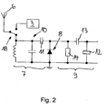
- Fig. 2
bis 7 - Schaltbilder von Empfängern zum Empfangen eines auf ein Funksignal amplitudenmodulierten Modulationssignals, die eine Gleichrichterschaltung aufweisen, die zur Anpassung ihrer Ausgangsimpedanz an die Eingangsimpedanz einer Detektionseinrichtung ein passives Filter hat,
- Fig.1
- a block diagram of an electronic device, which is connected via a UHF radio link to a base station, and
- Fig. 2 to 7
- Schematics of receivers for receiving a modulation signal modulated in amplitude to a radio signal, comprising a rectifier circuit having a passive filter for matching its output impedance to the input impedance of a detection device,
Ein als Funksensorknoten ausgestaltetes, in
Der elektrischen Schaltung ist eine in der Zeichnung nicht näher dargestellte Betriebsartenumschalteinrichtung zugeordnet, mittels der die Schaltung in einen Ruhezustand und in einen Arbeitszustand bringbar ist. Um Energie zu sparen, ist die Stromaufnahme der Schaltung im Ruhezustand gegenüber dem Arbeitszustand reduziert.The electrical circuit is associated with a not shown in the drawing operating mode switching device by means of which the circuit can be brought into a state of rest and in a working state. To save energy, the power consumption of the circuit is at rest compared to the working state reduced.
Das Gerät 1 hat außerdem einen Empfänger zum Empfangen eines von einer Basisstation 5 oder einem anderen Gerät 1 ausgesendeten Funksignals. Das Funksignal weist einen UHF-Träger auf, der mit einem etwa rechteckigen Modulationssignal amplitudenmoduliert ist. Die Trägerfrequenz des Trägers beträgt etwa 868 MHz. Das Modulationssignal hat ein Trägersignal von 125 kHz, das mit einem digitalen Informationssignal OOK-moduliert ist.The
In
Bei dem in
Bei dem in
Bei den in
In
Die Detektionseinrichtung 16 weist einen Aufweckempfänger vom Typ AS3932 des Herstellers austriamicrosystems auf Zum Aufwecken der im Ruhezustand befindlichen elektrischen Schaltung steht die Detektionseinrichtung 16 mit der Betriebsartenumschalteinrichtung in Steuerverbindung.The
Die Detektionseinrichtung 16 weist eine in der Zeichnung nicht näher dargestellte Demodulationseinrichtung zum Demodulieren des auf das 125 kHz-Trägersignal aufmodulierten OOK-Informationssignals auf Mit Hilfe der Demodulationseinrichtung kann das Informationssignal als digitales Signal in der Detektionseinrichtung 16 bereitgestellt werden.The
Die Demodulationseinrichtung ist mit einer Korrelationseinrichtung verbunden, die dazu dient, das Informationssignal mit einer vorbestimmten, dem elektronischen Gerät 1 eindeutig zugeordneten Adresssignal zu vergleichen. Das Adresssignal kann beispielsweise in einem nichtflüchtigen Datenspeicher abgelegt sein, aus dem es in die Korrelationseinrichtung geladen werden kann.The demodulation device is connected to a correlation device, which serves to compare the information signal with a predetermined, the
Die Korrelationseinrichtung steht derart mit der Betriebsartenumschalteinrichtung in Steuerverbindung, dass die elektrische Schaltung nur bei einer Übereinstimmung des Datensignals mit dem Adresssignal aufgeweckt wird.The correlation device is in control connection with the mode switching device such that the electrical circuit is woken up only if the data signal matches the address signal.
Bei den in
In
Bei den in
Bei dem Ausführungsbeispiel gemäß
In
Nachfolgend wird die Arbeitsweise des Geräts 1 beschrieben: Nach einem Reset des Mikrocomputers 2 fährt dieser entsprechend einem in einem Programmspeicher abgelegten Betriebsprogramm hoch. Auch der UHF-Transceiver 3, der einen Halbleiterchip vom Typ C1101 aufweist, und der Aufweckempfänger werden hochgefahren. Dabei werden Registereinstellungen vorgenommen. Mit Hilfe des Mikrocomputers 2 wird die Schalteinrichtung 18 so eingestellt, dass sie die UHF-Antenne 6 mit der Filterstufe 7 verbindet. Danach werden der UHF-Transceiver 3 und der Mikrocomputer 2 in den Ruhezustand versetzt. Die Detektionseinrichtung 16 bleibt aktiv, nimmt aber nur wenige µA Strom auf Während des Ruhemodus wird der logische Pegel am Steuereingang 18 der Schalteinrichtung 18 beibehalten.Hereinafter, the operation of the
Sobald über die UHF-Antenne 6 ein 868 MHz Funksignal empfangen wird, wird dieses über die Schalteinrichtung 18 und die passive Filterstufe 7 der Gleichrichterschaltung zugeführt. Das demodulierte Funksignal wird nach Filterung im passiven Filter 13 an den Eingang der Detektionseinrichtung angelegt. Wenn das Funksignal mit einem 125 kHz Modulationssignal amplitudenmoduliert ist, erkennt die Detektionseinrichtung 16 ein gültiges Aufwecksignal und dekodiert die Adresse. Wenn die Adresse mit der dem Gerät 1 zugeordneten Adresse übereinstimmt, sendet die Detektionseinrichtung 16 ein Aufwecksignal an den Mikrocomputer 2, woraufhin dieser in den Arbeitszustand geschaltet wird. Der Mikrocomputer 2 verbindet nun die UHF-Antenne 6 über die Schalteinrichtung 18 mit dem UHF-Transceiver 3. Außerdem übermittelt der Mikrocomputer 2 eine Bestätigungsmeldung über das Aufwecken an den UHF-Transceiver 3.As soon as an 868 MHz radio signal is received via the
Danach findet über den UHF-Transceiver 3 eine Datenkommunikation zwischen der Basisstation 5 oder dem weiteren Gerät und einem Sensor 20 statt, der über eine drahtgebundene Kommunikationsleitung an dem UHF-Transceiver 3 angeschlossen ist. Bei der Datenkommunikation können verschiedene Modulationsarten, Pakte-Handling und/oder CRC-Check zur Anwendung kommen.Thereafter, data communication takes place via the
Nach erfolgtem Datenaustausch verbindet der Mikrocomputer 2 die UHF-Antenne 6 wieder über die Schalteinrichtung 18 mit der passive Filterstufe. Außerdem werden der Mikrocomputer 2 und der UHF-Transceiver 3 in den Ruhezustand geschaltet.After the data exchange, the
Das Gerät 1 kann auch ein entsprechendes anderes Gerät aufwecken, indem der UHF-Transceiver 3 einen 868 MHz Träger bereitstellt, auf den durch Amplitudenmodulation ein Modulationssignal aufmoduliert wird, das zuvor mit einem Datensignal OOK-moduliert wurde, welches mit dem Adresssignal des anderen Geräts übereinstimmt. Dabei ist die UHF-Antenne 6 über die Schalteinrichtung 18 mit dem UHF-Transceiver 3 verbunden.The
Erwähnt werden soll noch, dass zwischen der UHF-Antenne und der Filterstufe 7 und/oder dem UHF-Transceiver ein hochohmiger, schmalbandiger UHF-Verstärker angeordnet sein kann.It should also be mentioned that a high-impedance, narrow-band UHF amplifier can be arranged between the UHF antenna and the
Claims (10)
- Electronic appliance (1) having an electrical circuit and an operating mode switching device which is associated with the latter and which can be used to wake the circuit from a quiescent state into an operating state in which the current draw of the circuit is greater than in the quiescent state, having a receiver for receiving a radio signal which has a UHF carrier which has been subjected to amplitude modulation with a modulation signal, wherein the receiver has a UHF antenna (6) which is connected to an input of a passive rectifier circuit (8) via a passive filter stage (7), wherein an output of the rectifier circuit (8) is connected to a detection device (16) for the modulation signal, and wherein the operating mode switching device has a control connection to the detection device (16) for the purpose of waking the electrical circuit which is in the quiescent state, characterized in that for the purpose of matching the output impedance of the rectifier circuit (8) to the input impedance of the detection device the output of the rectifier circuit (8) and the detection device (16) have a passive filter (9) arranged between them which passes the modulation signal, and in that the filter stage (7) and/or the filter (9) has/have an LC resonant circuit having a quartz oscillator (12) and/or a microacoustic resonator.
- Electronic appliance (1) according to Claim 1, characterized in that the filter (9) passes a modulation signal, the frequency or frequency range of which is between 10 kHz and 1.3 MHz, particularly above 30 kHz and preferably above 100 kHz.
- Electronic appliance (1) according to Claim 1 or 2, characterized in that the LC resonant circuit has a capacitance (13) which is connected in series with the quartz oscillator (12) and/or the microacoustic resonator in a current path which connects the UHF antenna (6) to a connection for a constant potential, and in that the quartz oscillator (12) and/or the microacoustic resonator and the capacitance (13) are connected to a node (17) which is connected to the input of the rectifier circuit (8).
- Electronic appliance (1) according to one of Claims 1 to 3, characterized in that the LC resonant circuit has a capacitance (13) which is connected in series with the quartz oscillator (12) and/or the microacoustic resonator in a current path which connects the output of the rectifier circuit (8) to a connection for a constant potential, and in that the quartz oscillator (12) and/or the microacoustic resonator and the capacitance (13) are connected to a node (15) to which the detection device (16) is connected.
- Electronic appliance (1) according to one of Claims 1 to 4, characterized in that the LC resonant circuit is a series resonant circuit which is arranged in a current path which connects the UHF antenna (6) to the passive rectifier circuit (8).
- Electronic appliance (1) according to Claim 5, characterized in that the current path which connects the UHF antenna (6) to the passive rectifier circuit (8) contains a switching apparatus which can be used to periodically interrupt this current path.
- Electronic appliance (1) according to one of Claims 1 to 6, characterized in that the modulation signal has a carrier signal which is modulated with an information signal, in that the detection device (16) has a demodulation device for demodulating the information signal, in that the detection device (16) has a correlation device for comparing the information signal with a predetermined address signal that is associated with the electronic appliance (1), and in that the correlation device has a control connection to the operating mode switching device such that the electrical circuit is woken only when the data signal matches the address signal.
- Electronic appliance (1) according to one of Claims 1 to 7, characterized in that it is in the form of a radio node in which the electrical circuit has a UHF transceiver that is connected to the UHF antenna.
- Electronic appliance (1) according to one of Claims 1 to 8, characterized in that the electrical circuit has a microcomputer (2).
- Electronic appliance (1) according to one of Claims 1 to 9, characterized in that the UHF antenna (6) can be selectively or alternately connected to the UHF transceiver (3) and the passive filter stage (7) by means of a switching device (18), and in that the switching device (18) has a control connection to the detection device (16) such that the UHF antenna (6) is connected to the passive filter stage (7) in the quiescent state of the electrical circuit and to the UHF transceiver (3) in the operating state.
Applications Claiming Priority (2)
| Application Number | Priority Date | Filing Date | Title |
|---|---|---|---|
| DE102010020733A DE102010020733A1 (en) | 2010-05-17 | 2010-05-17 | Electronic device |
| PCT/EP2011/002443 WO2011144320A1 (en) | 2010-05-17 | 2011-05-17 | Electronic device comprising an operating mode switching unit |
Publications (2)
| Publication Number | Publication Date |
|---|---|
| EP2572539A1 EP2572539A1 (en) | 2013-03-27 |
| EP2572539B1 true EP2572539B1 (en) | 2014-04-02 |
Family
ID=44454845
Family Applications (1)
| Application Number | Title | Priority Date | Filing Date |
|---|---|---|---|
| EP11727910.9A Active EP2572539B1 (en) | 2010-05-17 | 2011-05-17 | Electronic device comprising an operating mode switching unit |
Country Status (5)
| Country | Link |
|---|---|
| US (1) | US8958766B2 (en) |
| EP (1) | EP2572539B1 (en) |
| DE (1) | DE102010020733A1 (en) |
| ES (1) | ES2473268T3 (en) |
| WO (1) | WO2011144320A1 (en) |
Cited By (1)
| Publication number | Priority date | Publication date | Assignee | Title |
|---|---|---|---|---|
| EP3070982A1 (en) | 2015-03-19 | 2016-09-21 | Albert-Ludwigs-Universität Freiburg | Receiving device and method for operating a receiving device |
Families Citing this family (5)
| Publication number | Priority date | Publication date | Assignee | Title |
|---|---|---|---|---|
| DE102013220713B4 (en) * | 2013-10-14 | 2017-02-09 | Ihp Gmbh - Innovations For High Performance Microelectronics / Leibniz-Institut Für Innovative Mikroelektronik | Aufweckempfängerschaltung |
| JP6269863B2 (en) * | 2015-02-03 | 2018-01-31 | 株式会社村田製作所 | ANTENNA DEVICE AND ELECTRONIC DEVICE |
| US11211711B2 (en) | 2016-06-30 | 2021-12-28 | Hrl Laboratories, Llc | Antenna dynamically matched with electromechanical resonators |
| US11145982B2 (en) | 2016-06-30 | 2021-10-12 | Hrl Laboratories, Llc | Antenna loaded with electromechanical resonators |
| WO2023114304A1 (en) * | 2021-12-14 | 2023-06-22 | Northeastern University | Low impedance radio frequency antennas |
Family Cites Families (5)
| Publication number | Priority date | Publication date | Assignee | Title |
|---|---|---|---|---|
| EP0828306A3 (en) * | 1996-09-03 | 2000-03-22 | Lk-Products Oy | A matched impedance filter |
| SG54559A1 (en) * | 1996-09-13 | 1998-11-16 | Hitachi Ltd | Power transmission system ic card and information communication system using ic card |
| WO2004077761A1 (en) * | 2003-02-27 | 2004-09-10 | Nokia Corporation | Method and device for activating bluetooth devices through signaling |
| US7596367B2 (en) * | 2005-02-09 | 2009-09-29 | Sony Corporation | System and method for standby mode in directional signal receiver |
| CA2729910A1 (en) * | 2008-07-09 | 2010-01-14 | Secureall Corporation | Low power radio communication system |
-
2010
- 2010-05-17 DE DE102010020733A patent/DE102010020733A1/en not_active Ceased
-
2011
- 2011-05-17 EP EP11727910.9A patent/EP2572539B1/en active Active
- 2011-05-17 ES ES11727910.9T patent/ES2473268T3/en active Active
- 2011-05-17 WO PCT/EP2011/002443 patent/WO2011144320A1/en active Application Filing
-
2013
- 2013-01-14 US US13/740,435 patent/US8958766B2/en active Active
Cited By (3)
| Publication number | Priority date | Publication date | Assignee | Title |
|---|---|---|---|---|
| EP3070982A1 (en) | 2015-03-19 | 2016-09-21 | Albert-Ludwigs-Universität Freiburg | Receiving device and method for operating a receiving device |
| DE102015104141A1 (en) | 2015-03-19 | 2016-09-22 | Albert-Ludwigs-Universität Freiburg | Receiving device and method for operating a receiving device |
| US9985730B2 (en) | 2015-03-19 | 2018-05-29 | Albert-Ludwigs-Universität Freiburg | Wake-up circuit in receiving device and method of operating the receiving device |
Also Published As
| Publication number | Publication date |
|---|---|
| US8958766B2 (en) | 2015-02-17 |
| WO2011144320A1 (en) | 2011-11-24 |
| EP2572539A1 (en) | 2013-03-27 |
| ES2473268T3 (en) | 2014-07-04 |
| US20130130636A1 (en) | 2013-05-23 |
| DE102010020733A1 (en) | 2011-11-17 |
Similar Documents
| Publication | Publication Date | Title |
|---|---|---|
| EP2572539B1 (en) | Electronic device comprising an operating mode switching unit | |
| EP1691320B1 (en) | Circuitry and procedure for the power supply of a transponder | |
| DE60125100T2 (en) | Impedance matching network | |
| EP3966945B1 (en) | Tuning of an electromagnetic resonant circuit of a configuration interface of a subscriber of a communication system | |
| DE102014204065A1 (en) | CONTACTLESS COMMUNICATION DEVICE AND USER DEVICE CONTAINING THEREOF | |
| WO2009063056A1 (en) | Method for operating a field device, and communication unit and field device | |
| DE102008026845B3 (en) | Arrangement and method for reducing the power consumption of a control circuit | |
| DE112019003334T5 (en) | WIRELESS CHARGING SYSTEM WITH MULTIPLE COMMUNICATION MODES | |
| EP3918729B1 (en) | Bidirectional configuration of sensor nodes with mobile telephone without expansion | |
| DE102012214699A1 (en) | Electronic component circuit board with a radio-slave memory component | |
| DE10334765A1 (en) | Communication device for establishing a data connection between intelligent devices | |
| DE102010016066A1 (en) | Portable unit | |
| EP2591557A1 (en) | Energy-saving receiver assembly for the wireless reception of data | |
| EP3966944A1 (en) | Efficient communication for configuring sensor nodes | |
| DE102005028396B4 (en) | Transponder device and tire pressure monitoring system with transponder device | |
| DE102019217410A1 (en) | Configuration of a hardware component for the industrial control of a field device | |
| DE102013220713B4 (en) | Aufweckempfängerschaltung | |
| DE10119489C1 (en) | Transponder uses rectification of received HF interrogation pulses for providing operating energy eliminating need for battery | |
| EP2871616B1 (en) | Method and device for access control | |
| DE602005001243T2 (en) | Taktkalibrierungsverfahren a mobile phone, as well as mobile phone for it | |
| DE19528599A1 (en) | Method for controlling access from a terminal to mobile data carriers | |
| DE10231340B3 (en) | transponder circuit | |
| DE102022121872A1 (en) | DUAL BAND OPERATION OF A RADIO | |
| DE102021205187A1 (en) | WAVEFORM FOR A SIGNAL WITH CONSTANT ENVELOPE | |
| DE102006044015A1 (en) | Radio frequency transmitter and method for its operation |
Legal Events
| Date | Code | Title | Description |
|---|---|---|---|
| PUAI | Public reference made under article 153(3) epc to a published international application that has entered the european phase |
Free format text: ORIGINAL CODE: 0009012 |
|
| 17P | Request for examination filed |
Effective date: 20121207 |
|
| AK | Designated contracting states |
Kind code of ref document: A1 Designated state(s): AL AT BE BG CH CY CZ DE DK EE ES FI FR GB GR HR HU IE IS IT LI LT LU LV MC MK MT NL NO PL PT RO RS SE SI SK SM TR |
|
| DAX | Request for extension of the european patent (deleted) | ||
| RAP1 | Party data changed (applicant data changed or rights of an application transferred) |
Owner name: ALBERT-LUDWIGS-UNIVERSITAET FREIBURG |
|
| GRAP | Despatch of communication of intention to grant a patent |
Free format text: ORIGINAL CODE: EPIDOSNIGR1 |
|
| INTG | Intention to grant announced |
Effective date: 20131119 |
|
| GRAS | Grant fee paid |
Free format text: ORIGINAL CODE: EPIDOSNIGR3 |
|
| GRAA | (expected) grant |
Free format text: ORIGINAL CODE: 0009210 |
|
| AK | Designated contracting states |
Kind code of ref document: B1 Designated state(s): AL AT BE BG CH CY CZ DE DK EE ES FI FR GB GR HR HU IE IS IT LI LT LU LV MC MK MT NL NO PL PT RO RS SE SI SK SM TR |
|
| REG | Reference to a national code |
Ref country code: GB Ref legal event code: FG4D Free format text: NOT ENGLISH |
|
| REG | Reference to a national code |
Ref country code: AT Ref legal event code: REF Ref document number: 660762 Country of ref document: AT Kind code of ref document: T Effective date: 20140415 Ref country code: CH Ref legal event code: EP |
|
| REG | Reference to a national code |
Ref country code: IE Ref legal event code: FG4D Free format text: LANGUAGE OF EP DOCUMENT: GERMAN |
|
| REG | Reference to a national code |
Ref country code: DE Ref legal event code: R096 Ref document number: 502011002623 Country of ref document: DE Effective date: 20140522 |
|
| REG | Reference to a national code |
Ref country code: ES Ref legal event code: FG2A Ref document number: 2473268 Country of ref document: ES Kind code of ref document: T3 Effective date: 20140704 |
|
| REG | Reference to a national code |
Ref country code: NL Ref legal event code: VDEP Effective date: 20140402 |
|
| REG | Reference to a national code |
Ref country code: LT Ref legal event code: MG4D |
|
| REG | Reference to a national code |
Ref country code: CH Ref legal event code: NV Representative=s name: PATENTANWALT DIPL.-ING. (UNI.) WOLFGANG HEISEL, CH |
|
| PG25 | Lapsed in a contracting state [announced via postgrant information from national office to epo] |
Ref country code: GR Free format text: LAPSE BECAUSE OF FAILURE TO SUBMIT A TRANSLATION OF THE DESCRIPTION OR TO PAY THE FEE WITHIN THE PRESCRIBED TIME-LIMIT Effective date: 20140703 Ref country code: NO Free format text: LAPSE BECAUSE OF FAILURE TO SUBMIT A TRANSLATION OF THE DESCRIPTION OR TO PAY THE FEE WITHIN THE PRESCRIBED TIME-LIMIT Effective date: 20140702 Ref country code: CY Free format text: LAPSE BECAUSE OF FAILURE TO SUBMIT A TRANSLATION OF THE DESCRIPTION OR TO PAY THE FEE WITHIN THE PRESCRIBED TIME-LIMIT Effective date: 20140402 Ref country code: NL Free format text: LAPSE BECAUSE OF FAILURE TO SUBMIT A TRANSLATION OF THE DESCRIPTION OR TO PAY THE FEE WITHIN THE PRESCRIBED TIME-LIMIT Effective date: 20140402 Ref country code: IS Free format text: LAPSE BECAUSE OF FAILURE TO SUBMIT A TRANSLATION OF THE DESCRIPTION OR TO PAY THE FEE WITHIN THE PRESCRIBED TIME-LIMIT Effective date: 20140802 Ref country code: LT Free format text: LAPSE BECAUSE OF FAILURE TO SUBMIT A TRANSLATION OF THE DESCRIPTION OR TO PAY THE FEE WITHIN THE PRESCRIBED TIME-LIMIT Effective date: 20140402 Ref country code: FI Free format text: LAPSE BECAUSE OF FAILURE TO SUBMIT A TRANSLATION OF THE DESCRIPTION OR TO PAY THE FEE WITHIN THE PRESCRIBED TIME-LIMIT Effective date: 20140402 Ref country code: CZ Free format text: LAPSE BECAUSE OF FAILURE TO SUBMIT A TRANSLATION OF THE DESCRIPTION OR TO PAY THE FEE WITHIN THE PRESCRIBED TIME-LIMIT Effective date: 20140402 Ref country code: BG Free format text: LAPSE BECAUSE OF FAILURE TO SUBMIT A TRANSLATION OF THE DESCRIPTION OR TO PAY THE FEE WITHIN THE PRESCRIBED TIME-LIMIT Effective date: 20140702 |
|
| PG25 | Lapsed in a contracting state [announced via postgrant information from national office to epo] |
Ref country code: HR Free format text: LAPSE BECAUSE OF FAILURE TO SUBMIT A TRANSLATION OF THE DESCRIPTION OR TO PAY THE FEE WITHIN THE PRESCRIBED TIME-LIMIT Effective date: 20140402 Ref country code: RS Free format text: LAPSE BECAUSE OF FAILURE TO SUBMIT A TRANSLATION OF THE DESCRIPTION OR TO PAY THE FEE WITHIN THE PRESCRIBED TIME-LIMIT Effective date: 20140402 Ref country code: SE Free format text: LAPSE BECAUSE OF FAILURE TO SUBMIT A TRANSLATION OF THE DESCRIPTION OR TO PAY THE FEE WITHIN THE PRESCRIBED TIME-LIMIT Effective date: 20140402 Ref country code: LV Free format text: LAPSE BECAUSE OF FAILURE TO SUBMIT A TRANSLATION OF THE DESCRIPTION OR TO PAY THE FEE WITHIN THE PRESCRIBED TIME-LIMIT Effective date: 20140402 Ref country code: PL Free format text: LAPSE BECAUSE OF FAILURE TO SUBMIT A TRANSLATION OF THE DESCRIPTION OR TO PAY THE FEE WITHIN THE PRESCRIBED TIME-LIMIT Effective date: 20140402 |
|
| PG25 | Lapsed in a contracting state [announced via postgrant information from national office to epo] |
Ref country code: PT Free format text: LAPSE BECAUSE OF FAILURE TO SUBMIT A TRANSLATION OF THE DESCRIPTION OR TO PAY THE FEE WITHIN THE PRESCRIBED TIME-LIMIT Effective date: 20140804 |
|
| REG | Reference to a national code |
Ref country code: DE Ref legal event code: R097 Ref document number: 502011002623 Country of ref document: DE |
|
| PG25 | Lapsed in a contracting state [announced via postgrant information from national office to epo] |
Ref country code: DK Free format text: LAPSE BECAUSE OF FAILURE TO SUBMIT A TRANSLATION OF THE DESCRIPTION OR TO PAY THE FEE WITHIN THE PRESCRIBED TIME-LIMIT Effective date: 20140402 Ref country code: MC Free format text: LAPSE BECAUSE OF FAILURE TO SUBMIT A TRANSLATION OF THE DESCRIPTION OR TO PAY THE FEE WITHIN THE PRESCRIBED TIME-LIMIT Effective date: 20140402 Ref country code: RO Free format text: LAPSE BECAUSE OF FAILURE TO SUBMIT A TRANSLATION OF THE DESCRIPTION OR TO PAY THE FEE WITHIN THE PRESCRIBED TIME-LIMIT Effective date: 20140402 Ref country code: EE Free format text: LAPSE BECAUSE OF FAILURE TO SUBMIT A TRANSLATION OF THE DESCRIPTION OR TO PAY THE FEE WITHIN THE PRESCRIBED TIME-LIMIT Effective date: 20140402 Ref country code: SK Free format text: LAPSE BECAUSE OF FAILURE TO SUBMIT A TRANSLATION OF THE DESCRIPTION OR TO PAY THE FEE WITHIN THE PRESCRIBED TIME-LIMIT Effective date: 20140402 |
|
| PLBE | No opposition filed within time limit |
Free format text: ORIGINAL CODE: 0009261 |
|
| STAA | Information on the status of an ep patent application or granted ep patent |
Free format text: STATUS: NO OPPOSITION FILED WITHIN TIME LIMIT |
|
| REG | Reference to a national code |
Ref country code: IE Ref legal event code: MM4A |
|
| 26N | No opposition filed |
Effective date: 20150106 |
|
| PG25 | Lapsed in a contracting state [announced via postgrant information from national office to epo] |
Ref country code: IT Free format text: LAPSE BECAUSE OF FAILURE TO SUBMIT A TRANSLATION OF THE DESCRIPTION OR TO PAY THE FEE WITHIN THE PRESCRIBED TIME-LIMIT Effective date: 20140402 |
|
| REG | Reference to a national code |
Ref country code: DE Ref legal event code: R097 Ref document number: 502011002623 Country of ref document: DE Effective date: 20150106 |
|
| PG25 | Lapsed in a contracting state [announced via postgrant information from national office to epo] |
Ref country code: IE Free format text: LAPSE BECAUSE OF NON-PAYMENT OF DUE FEES Effective date: 20140517 |
|
| PG25 | Lapsed in a contracting state [announced via postgrant information from national office to epo] |
Ref country code: RS Free format text: LAPSE BECAUSE OF FAILURE TO SUBMIT A TRANSLATION OF THE DESCRIPTION OR TO PAY THE FEE WITHIN THE PRESCRIBED TIME-LIMIT Effective date: 20141119 |
|
| PG25 | Lapsed in a contracting state [announced via postgrant information from national office to epo] |
Ref country code: SI Free format text: LAPSE BECAUSE OF FAILURE TO SUBMIT A TRANSLATION OF THE DESCRIPTION OR TO PAY THE FEE WITHIN THE PRESCRIBED TIME-LIMIT Effective date: 20140402 |
|
| PG25 | Lapsed in a contracting state [announced via postgrant information from national office to epo] |
Ref country code: MT Free format text: LAPSE BECAUSE OF FAILURE TO SUBMIT A TRANSLATION OF THE DESCRIPTION OR TO PAY THE FEE WITHIN THE PRESCRIBED TIME-LIMIT Effective date: 20140402 |
|
| PG25 | Lapsed in a contracting state [announced via postgrant information from national office to epo] |
Ref country code: SM Free format text: LAPSE BECAUSE OF FAILURE TO SUBMIT A TRANSLATION OF THE DESCRIPTION OR TO PAY THE FEE WITHIN THE PRESCRIBED TIME-LIMIT Effective date: 20140402 |
|
| REG | Reference to a national code |
Ref country code: FR Ref legal event code: PLFP Year of fee payment: 6 |
|
| PG25 | Lapsed in a contracting state [announced via postgrant information from national office to epo] |
Ref country code: BE Free format text: LAPSE BECAUSE OF FAILURE TO SUBMIT A TRANSLATION OF THE DESCRIPTION OR TO PAY THE FEE WITHIN THE PRESCRIBED TIME-LIMIT Effective date: 20140531 Ref country code: HU Free format text: LAPSE BECAUSE OF FAILURE TO SUBMIT A TRANSLATION OF THE DESCRIPTION OR TO PAY THE FEE WITHIN THE PRESCRIBED TIME-LIMIT; INVALID AB INITIO Effective date: 20110517 Ref country code: LU Free format text: LAPSE BECAUSE OF NON-PAYMENT OF DUE FEES Effective date: 20140517 Ref country code: TR Free format text: LAPSE BECAUSE OF FAILURE TO SUBMIT A TRANSLATION OF THE DESCRIPTION OR TO PAY THE FEE WITHIN THE PRESCRIBED TIME-LIMIT Effective date: 20140402 |
|
| REG | Reference to a national code |
Ref country code: FR Ref legal event code: PLFP Year of fee payment: 7 |
|
| REG | Reference to a national code |
Ref country code: FR Ref legal event code: PLFP Year of fee payment: 8 |
|
| PG25 | Lapsed in a contracting state [announced via postgrant information from national office to epo] |
Ref country code: MK Free format text: LAPSE BECAUSE OF FAILURE TO SUBMIT A TRANSLATION OF THE DESCRIPTION OR TO PAY THE FEE WITHIN THE PRESCRIBED TIME-LIMIT Effective date: 20140402 |
|
| PG25 | Lapsed in a contracting state [announced via postgrant information from national office to epo] |
Ref country code: AL Free format text: LAPSE BECAUSE OF FAILURE TO SUBMIT A TRANSLATION OF THE DESCRIPTION OR TO PAY THE FEE WITHIN THE PRESCRIBED TIME-LIMIT Effective date: 20140402 |
|
| REG | Reference to a national code |
Ref country code: DE Ref legal event code: R082 Ref document number: 502011002623 Country of ref document: DE |
|
| PGFP | Annual fee paid to national office [announced via postgrant information from national office to epo] |
Ref country code: FR Payment date: 20230517 Year of fee payment: 13 Ref country code: ES Payment date: 20230621 Year of fee payment: 13 Ref country code: CH Payment date: 20230602 Year of fee payment: 13 |
|
| PGFP | Annual fee paid to national office [announced via postgrant information from national office to epo] |
Ref country code: GB Payment date: 20230522 Year of fee payment: 13 |
|
| PGFP | Annual fee paid to national office [announced via postgrant information from national office to epo] |
Ref country code: DE Payment date: 20240517 Year of fee payment: 14 |
|
| PGFP | Annual fee paid to national office [announced via postgrant information from national office to epo] |
Ref country code: AT Payment date: 20240517 Year of fee payment: 14 |