EP2570521A2 - Manufacturing method of group 13 nitride crystal - Google Patents
Manufacturing method of group 13 nitride crystal Download PDFInfo
- Publication number
- EP2570521A2 EP2570521A2 EP12181565A EP12181565A EP2570521A2 EP 2570521 A2 EP2570521 A2 EP 2570521A2 EP 12181565 A EP12181565 A EP 12181565A EP 12181565 A EP12181565 A EP 12181565A EP 2570521 A2 EP2570521 A2 EP 2570521A2
- Authority
- EP
- European Patent Office
- Prior art keywords
- crystal
- group
- nitride crystal
- plane
- gallium nitride
- Prior art date
- Legal status (The legal status is an assumption and is not a legal conclusion. Google has not performed a legal analysis and makes no representation as to the accuracy of the status listed.)
- Withdrawn
Links
- 239000013078 crystal Substances 0.000 title claims abstract description 721
- 150000004767 nitrides Chemical class 0.000 title claims abstract description 159
- 238000004519 manufacturing process Methods 0.000 title claims abstract description 57
- JMASRVWKEDWRBT-UHFFFAOYSA-N Gallium nitride Chemical compound [Ga]#N JMASRVWKEDWRBT-UHFFFAOYSA-N 0.000 claims abstract description 152
- 229910002601 GaN Inorganic materials 0.000 claims abstract description 150
- 238000000034 method Methods 0.000 claims abstract description 117
- 230000012010 growth Effects 0.000 claims abstract description 95
- 230000008569 process Effects 0.000 claims abstract description 82
- IJGRMHOSHXDMSA-UHFFFAOYSA-N Atomic nitrogen Chemical compound N#N IJGRMHOSHXDMSA-UHFFFAOYSA-N 0.000 claims description 101
- 239000000463 material Substances 0.000 claims description 65
- 239000007789 gas Substances 0.000 claims description 59
- 239000000203 mixture Substances 0.000 claims description 57
- 229910052757 nitrogen Inorganic materials 0.000 claims description 39
- 229910052783 alkali metal Inorganic materials 0.000 claims description 22
- 150000001340 alkali metals Chemical class 0.000 claims description 22
- 229910052795 boron group element Inorganic materials 0.000 claims description 14
- 238000011900 installation process Methods 0.000 claims description 3
- 239000000758 substrate Substances 0.000 description 94
- ZOXJGFHDIHLPTG-UHFFFAOYSA-N Boron Chemical compound [B] ZOXJGFHDIHLPTG-UHFFFAOYSA-N 0.000 description 66
- 229910052796 boron Inorganic materials 0.000 description 66
- 239000003085 diluting agent Substances 0.000 description 22
- 229910001873 dinitrogen Inorganic materials 0.000 description 21
- 239000011734 sodium Substances 0.000 description 17
- 238000005424 photoluminescence Methods 0.000 description 16
- PZNSFCLAULLKQX-UHFFFAOYSA-N Boron nitride Chemical compound N#B PZNSFCLAULLKQX-UHFFFAOYSA-N 0.000 description 15
- GYHNNYVSQQEPJS-UHFFFAOYSA-N Gallium Chemical compound [Ga] GYHNNYVSQQEPJS-UHFFFAOYSA-N 0.000 description 14
- DGAQECJNVWCQMB-PUAWFVPOSA-M Ilexoside XXIX Chemical compound C[C@@H]1CC[C@@]2(CC[C@@]3(C(=CC[C@H]4[C@]3(CC[C@@H]5[C@@]4(CC[C@@H](C5(C)C)OS(=O)(=O)[O-])C)C)[C@@H]2[C@]1(C)O)C)C(=O)O[C@H]6[C@@H]([C@H]([C@@H]([C@H](O6)CO)O)O)O.[Na+] DGAQECJNVWCQMB-PUAWFVPOSA-M 0.000 description 14
- 229910052733 gallium Inorganic materials 0.000 description 14
- 229910052708 sodium Inorganic materials 0.000 description 14
- 229910052582 BN Inorganic materials 0.000 description 13
- 238000000295 emission spectrum Methods 0.000 description 13
- 230000004907 flux Effects 0.000 description 11
- 238000005259 measurement Methods 0.000 description 11
- XKRFYHLGVUSROY-UHFFFAOYSA-N Argon Chemical compound [Ar] XKRFYHLGVUSROY-UHFFFAOYSA-N 0.000 description 10
- 230000001276 controlling effect Effects 0.000 description 10
- 238000007716 flux method Methods 0.000 description 10
- 239000012535 impurity Substances 0.000 description 10
- 239000000654 additive Substances 0.000 description 9
- 238000010894 electron beam technology Methods 0.000 description 9
- 230000005284 excitation Effects 0.000 description 9
- 238000010309 melting process Methods 0.000 description 9
- PXIPVTKHYLBLMZ-UHFFFAOYSA-N Sodium azide Chemical compound [Na+].[N-]=[N+]=[N-] PXIPVTKHYLBLMZ-UHFFFAOYSA-N 0.000 description 8
- 239000012298 atmosphere Substances 0.000 description 8
- 230000007547 defect Effects 0.000 description 8
- 230000003595 spectral effect Effects 0.000 description 7
- 229910052784 alkaline earth metal Inorganic materials 0.000 description 6
- PMHQVHHXPFUNSP-UHFFFAOYSA-M copper(1+);methylsulfanylmethane;bromide Chemical compound Br[Cu].CSC PMHQVHHXPFUNSP-UHFFFAOYSA-M 0.000 description 6
- 239000011261 inert gas Substances 0.000 description 6
- 239000011777 magnesium Substances 0.000 description 6
- 239000004065 semiconductor Substances 0.000 description 6
- 229910052782 aluminium Inorganic materials 0.000 description 5
- XAGFODPZIPBFFR-UHFFFAOYSA-N aluminium Chemical compound [Al] XAGFODPZIPBFFR-UHFFFAOYSA-N 0.000 description 5
- 229910052786 argon Inorganic materials 0.000 description 5
- 150000001875 compounds Chemical class 0.000 description 5
- 238000013507 mapping Methods 0.000 description 5
- 230000035040 seed growth Effects 0.000 description 5
- WHXSMMKQMYFTQS-UHFFFAOYSA-N Lithium Chemical compound [Li] WHXSMMKQMYFTQS-UHFFFAOYSA-N 0.000 description 4
- FYYHWMGAXLPEAU-UHFFFAOYSA-N Magnesium Chemical compound [Mg] FYYHWMGAXLPEAU-UHFFFAOYSA-N 0.000 description 4
- NBIIXXVUZAFLBC-UHFFFAOYSA-N Phosphoric acid Chemical compound OP(O)(O)=O NBIIXXVUZAFLBC-UHFFFAOYSA-N 0.000 description 4
- QAOWNCQODCNURD-UHFFFAOYSA-N Sulfuric acid Chemical compound OS(O)(=O)=O QAOWNCQODCNURD-UHFFFAOYSA-N 0.000 description 4
- 239000002253 acid Substances 0.000 description 4
- JNDMLEXHDPKVFC-UHFFFAOYSA-N aluminum;oxygen(2-);yttrium(3+) Chemical compound [O-2].[O-2].[O-2].[Al+3].[Y+3] JNDMLEXHDPKVFC-UHFFFAOYSA-N 0.000 description 4
- 239000011575 calcium Substances 0.000 description 4
- 239000011651 chromium Substances 0.000 description 4
- 238000005520 cutting process Methods 0.000 description 4
- 230000008020 evaporation Effects 0.000 description 4
- 238000001704 evaporation Methods 0.000 description 4
- 238000010438 heat treatment Methods 0.000 description 4
- 229910052738 indium Inorganic materials 0.000 description 4
- APFVFJFRJDLVQX-UHFFFAOYSA-N indium atom Chemical compound [In] APFVFJFRJDLVQX-UHFFFAOYSA-N 0.000 description 4
- 238000009434 installation Methods 0.000 description 4
- 229910052744 lithium Inorganic materials 0.000 description 4
- 229910052749 magnesium Inorganic materials 0.000 description 4
- 239000011572 manganese Substances 0.000 description 4
- 230000001105 regulatory effect Effects 0.000 description 4
- 229910052594 sapphire Inorganic materials 0.000 description 4
- 239000010980 sapphire Substances 0.000 description 4
- 229910052712 strontium Inorganic materials 0.000 description 4
- CIOAGBVUUVVLOB-UHFFFAOYSA-N strontium atom Chemical compound [Sr] CIOAGBVUUVVLOB-UHFFFAOYSA-N 0.000 description 4
- 229910019901 yttrium aluminum garnet Inorganic materials 0.000 description 4
- ZLMJMSJWJFRBEC-UHFFFAOYSA-N Potassium Chemical compound [K] ZLMJMSJWJFRBEC-UHFFFAOYSA-N 0.000 description 3
- PNEYBMLMFCGWSK-UHFFFAOYSA-N aluminium oxide Inorganic materials [O-2].[O-2].[O-2].[Al+3].[Al+3] PNEYBMLMFCGWSK-UHFFFAOYSA-N 0.000 description 3
- 238000010276 construction Methods 0.000 description 3
- 229910021482 group 13 metal Inorganic materials 0.000 description 3
- 125000005842 heteroatom Chemical group 0.000 description 3
- 238000002248 hydride vapour-phase epitaxy Methods 0.000 description 3
- 239000007791 liquid phase Substances 0.000 description 3
- 238000002844 melting Methods 0.000 description 3
- 230000008018 melting Effects 0.000 description 3
- 238000005498 polishing Methods 0.000 description 3
- 229910052700 potassium Inorganic materials 0.000 description 3
- 239000011591 potassium Substances 0.000 description 3
- 230000000717 retained effect Effects 0.000 description 3
- -1 sintered BN Chemical class 0.000 description 3
- PIGFYZPCRLYGLF-UHFFFAOYSA-N Aluminum nitride Chemical compound [Al]#N PIGFYZPCRLYGLF-UHFFFAOYSA-N 0.000 description 2
- OYPRJOBELJOOCE-UHFFFAOYSA-N Calcium Chemical compound [Ca] OYPRJOBELJOOCE-UHFFFAOYSA-N 0.000 description 2
- VYZAMTAEIAYCRO-UHFFFAOYSA-N Chromium Chemical compound [Cr] VYZAMTAEIAYCRO-UHFFFAOYSA-N 0.000 description 2
- 229910052691 Erbium Inorganic materials 0.000 description 2
- 229910052693 Europium Inorganic materials 0.000 description 2
- XEEYBQQBJWHFJM-UHFFFAOYSA-N Iron Chemical compound [Fe] XEEYBQQBJWHFJM-UHFFFAOYSA-N 0.000 description 2
- PWHULOQIROXLJO-UHFFFAOYSA-N Manganese Chemical compound [Mn] PWHULOQIROXLJO-UHFFFAOYSA-N 0.000 description 2
- XUIMIQQOPSSXEZ-UHFFFAOYSA-N Silicon Chemical compound [Si] XUIMIQQOPSSXEZ-UHFFFAOYSA-N 0.000 description 2
- 229910052771 Terbium Inorganic materials 0.000 description 2
- 229910052775 Thulium Inorganic materials 0.000 description 2
- 229910000147 aluminium phosphate Inorganic materials 0.000 description 2
- QVGXLLKOCUKJST-UHFFFAOYSA-N atomic oxygen Chemical compound [O] QVGXLLKOCUKJST-UHFFFAOYSA-N 0.000 description 2
- 229910052788 barium Inorganic materials 0.000 description 2
- DSAJWYNOEDNPEQ-UHFFFAOYSA-N barium atom Chemical compound [Ba] DSAJWYNOEDNPEQ-UHFFFAOYSA-N 0.000 description 2
- UIZLQMLDSWKZGC-UHFFFAOYSA-N cadmium helium Chemical compound [He].[Cd] UIZLQMLDSWKZGC-UHFFFAOYSA-N 0.000 description 2
- 229910052791 calcium Inorganic materials 0.000 description 2
- 229910052804 chromium Inorganic materials 0.000 description 2
- 239000003086 colorant Substances 0.000 description 2
- 239000000039 congener Substances 0.000 description 2
- 239000000470 constituent Substances 0.000 description 2
- 230000007423 decrease Effects 0.000 description 2
- 238000001739 density measurement Methods 0.000 description 2
- 230000000694 effects Effects 0.000 description 2
- UYAHIZSMUZPPFV-UHFFFAOYSA-N erbium Chemical compound [Er] UYAHIZSMUZPPFV-UHFFFAOYSA-N 0.000 description 2
- OGPBJKLSAFTDLK-UHFFFAOYSA-N europium atom Chemical compound [Eu] OGPBJKLSAFTDLK-UHFFFAOYSA-N 0.000 description 2
- 239000007792 gaseous phase Substances 0.000 description 2
- 229910052732 germanium Inorganic materials 0.000 description 2
- GNPVGFCGXDBREM-UHFFFAOYSA-N germanium atom Chemical compound [Ge] GNPVGFCGXDBREM-UHFFFAOYSA-N 0.000 description 2
- 239000001307 helium Substances 0.000 description 2
- 229910052734 helium Inorganic materials 0.000 description 2
- SWQJXJOGLNCZEY-UHFFFAOYSA-N helium atom Chemical compound [He] SWQJXJOGLNCZEY-UHFFFAOYSA-N 0.000 description 2
- 238000005286 illumination Methods 0.000 description 2
- 150000002500 ions Chemical group 0.000 description 2
- 239000004973 liquid crystal related substance Substances 0.000 description 2
- 229910052748 manganese Inorganic materials 0.000 description 2
- 238000001451 molecular beam epitaxy Methods 0.000 description 2
- 238000012544 monitoring process Methods 0.000 description 2
- 239000001301 oxygen Substances 0.000 description 2
- 229910052760 oxygen Inorganic materials 0.000 description 2
- 229910052761 rare earth metal Inorganic materials 0.000 description 2
- 230000009467 reduction Effects 0.000 description 2
- 229910052710 silicon Inorganic materials 0.000 description 2
- 239000010703 silicon Substances 0.000 description 2
- 229910001220 stainless steel Inorganic materials 0.000 description 2
- 239000010935 stainless steel Substances 0.000 description 2
- JBQYATWDVHIOAR-UHFFFAOYSA-N tellanylidenegermanium Chemical compound [Te]=[Ge] JBQYATWDVHIOAR-UHFFFAOYSA-N 0.000 description 2
- GZCRRIHWUXGPOV-UHFFFAOYSA-N terbium atom Chemical compound [Tb] GZCRRIHWUXGPOV-UHFFFAOYSA-N 0.000 description 2
- FRNOGLGSGLTDKL-UHFFFAOYSA-N thulium atom Chemical compound [Tm] FRNOGLGSGLTDKL-UHFFFAOYSA-N 0.000 description 2
- 229910052723 transition metal Inorganic materials 0.000 description 2
- 150000003624 transition metals Chemical class 0.000 description 2
- OKTJSMMVPCPJKN-UHFFFAOYSA-N Carbon Chemical compound [C] OKTJSMMVPCPJKN-UHFFFAOYSA-N 0.000 description 1
- 229910001218 Gallium arsenide Inorganic materials 0.000 description 1
- 208000012868 Overgrowth Diseases 0.000 description 1
- 235000005811 Viola adunca Nutrition 0.000 description 1
- 240000009038 Viola odorata Species 0.000 description 1
- 235000013487 Viola odorata Nutrition 0.000 description 1
- 235000002254 Viola papilionacea Nutrition 0.000 description 1
- 230000000996 additive effect Effects 0.000 description 1
- 229910001417 caesium ion Inorganic materials 0.000 description 1
- 229910052799 carbon Inorganic materials 0.000 description 1
- 238000005229 chemical vapour deposition Methods 0.000 description 1
- 238000007796 conventional method Methods 0.000 description 1
- 238000001816 cooling Methods 0.000 description 1
- 230000003247 decreasing effect Effects 0.000 description 1
- 238000001514 detection method Methods 0.000 description 1
- 238000009826 distribution Methods 0.000 description 1
- 239000002019 doping agent Substances 0.000 description 1
- 238000005516 engineering process Methods 0.000 description 1
- 238000010884 ion-beam technique Methods 0.000 description 1
- 239000007788 liquid Substances 0.000 description 1
- 229910052751 metal Inorganic materials 0.000 description 1
- 239000002184 metal Substances 0.000 description 1
- 150000001247 metal acetylides Chemical class 0.000 description 1
- 238000012986 modification Methods 0.000 description 1
- 230000004048 modification Effects 0.000 description 1
- 238000009740 moulding (composite fabrication) Methods 0.000 description 1
- 239000012299 nitrogen atmosphere Substances 0.000 description 1
- 230000000737 periodic effect Effects 0.000 description 1
- 238000002360 preparation method Methods 0.000 description 1
- 238000012545 processing Methods 0.000 description 1
- 230000006798 recombination Effects 0.000 description 1
- 238000005215 recombination Methods 0.000 description 1
- 238000007493 shaping process Methods 0.000 description 1
- 150000003388 sodium compounds Chemical class 0.000 description 1
- 238000001228 spectrum Methods 0.000 description 1
- 238000004381 surface treatment Methods 0.000 description 1
- 230000008646 thermal stress Effects 0.000 description 1
- 238000011282 treatment Methods 0.000 description 1
- 238000001947 vapour-phase growth Methods 0.000 description 1
Images






Classifications
-
- C—CHEMISTRY; METALLURGY
- C30—CRYSTAL GROWTH
- C30B—SINGLE-CRYSTAL GROWTH; UNIDIRECTIONAL SOLIDIFICATION OF EUTECTIC MATERIAL OR UNIDIRECTIONAL DEMIXING OF EUTECTOID MATERIAL; REFINING BY ZONE-MELTING OF MATERIAL; PRODUCTION OF A HOMOGENEOUS POLYCRYSTALLINE MATERIAL WITH DEFINED STRUCTURE; SINGLE CRYSTALS OR HOMOGENEOUS POLYCRYSTALLINE MATERIAL WITH DEFINED STRUCTURE; AFTER-TREATMENT OF SINGLE CRYSTALS OR A HOMOGENEOUS POLYCRYSTALLINE MATERIAL WITH DEFINED STRUCTURE; APPARATUS THEREFOR
- C30B9/00—Single-crystal growth from melt solutions using molten solvents
- C30B9/04—Single-crystal growth from melt solutions using molten solvents by cooling of the solution
- C30B9/08—Single-crystal growth from melt solutions using molten solvents by cooling of the solution using other solvents
- C30B9/12—Salt solvents, e.g. flux growth
-
- C—CHEMISTRY; METALLURGY
- C30—CRYSTAL GROWTH
- C30B—SINGLE-CRYSTAL GROWTH; UNIDIRECTIONAL SOLIDIFICATION OF EUTECTIC MATERIAL OR UNIDIRECTIONAL DEMIXING OF EUTECTOID MATERIAL; REFINING BY ZONE-MELTING OF MATERIAL; PRODUCTION OF A HOMOGENEOUS POLYCRYSTALLINE MATERIAL WITH DEFINED STRUCTURE; SINGLE CRYSTALS OR HOMOGENEOUS POLYCRYSTALLINE MATERIAL WITH DEFINED STRUCTURE; AFTER-TREATMENT OF SINGLE CRYSTALS OR A HOMOGENEOUS POLYCRYSTALLINE MATERIAL WITH DEFINED STRUCTURE; APPARATUS THEREFOR
- C30B29/00—Single crystals or homogeneous polycrystalline material with defined structure characterised by the material or by their shape
- C30B29/10—Inorganic compounds or compositions
- C30B29/38—Nitrides
-
- C—CHEMISTRY; METALLURGY
- C30—CRYSTAL GROWTH
- C30B—SINGLE-CRYSTAL GROWTH; UNIDIRECTIONAL SOLIDIFICATION OF EUTECTIC MATERIAL OR UNIDIRECTIONAL DEMIXING OF EUTECTOID MATERIAL; REFINING BY ZONE-MELTING OF MATERIAL; PRODUCTION OF A HOMOGENEOUS POLYCRYSTALLINE MATERIAL WITH DEFINED STRUCTURE; SINGLE CRYSTALS OR HOMOGENEOUS POLYCRYSTALLINE MATERIAL WITH DEFINED STRUCTURE; AFTER-TREATMENT OF SINGLE CRYSTALS OR A HOMOGENEOUS POLYCRYSTALLINE MATERIAL WITH DEFINED STRUCTURE; APPARATUS THEREFOR
- C30B19/00—Liquid-phase epitaxial-layer growth
-
- C—CHEMISTRY; METALLURGY
- C30—CRYSTAL GROWTH
- C30B—SINGLE-CRYSTAL GROWTH; UNIDIRECTIONAL SOLIDIFICATION OF EUTECTIC MATERIAL OR UNIDIRECTIONAL DEMIXING OF EUTECTOID MATERIAL; REFINING BY ZONE-MELTING OF MATERIAL; PRODUCTION OF A HOMOGENEOUS POLYCRYSTALLINE MATERIAL WITH DEFINED STRUCTURE; SINGLE CRYSTALS OR HOMOGENEOUS POLYCRYSTALLINE MATERIAL WITH DEFINED STRUCTURE; AFTER-TREATMENT OF SINGLE CRYSTALS OR A HOMOGENEOUS POLYCRYSTALLINE MATERIAL WITH DEFINED STRUCTURE; APPARATUS THEREFOR
- C30B29/00—Single crystals or homogeneous polycrystalline material with defined structure characterised by the material or by their shape
- C30B29/10—Inorganic compounds or compositions
- C30B29/40—AIIIBV compounds wherein A is B, Al, Ga, In or Tl and B is N, P, As, Sb or Bi
- C30B29/403—AIII-nitrides
- C30B29/406—Gallium nitride
-
- C—CHEMISTRY; METALLURGY
- C30—CRYSTAL GROWTH
- C30B—SINGLE-CRYSTAL GROWTH; UNIDIRECTIONAL SOLIDIFICATION OF EUTECTIC MATERIAL OR UNIDIRECTIONAL DEMIXING OF EUTECTOID MATERIAL; REFINING BY ZONE-MELTING OF MATERIAL; PRODUCTION OF A HOMOGENEOUS POLYCRYSTALLINE MATERIAL WITH DEFINED STRUCTURE; SINGLE CRYSTALS OR HOMOGENEOUS POLYCRYSTALLINE MATERIAL WITH DEFINED STRUCTURE; AFTER-TREATMENT OF SINGLE CRYSTALS OR A HOMOGENEOUS POLYCRYSTALLINE MATERIAL WITH DEFINED STRUCTURE; APPARATUS THEREFOR
- C30B9/00—Single-crystal growth from melt solutions using molten solvents
- C30B9/04—Single-crystal growth from melt solutions using molten solvents by cooling of the solution
- C30B9/08—Single-crystal growth from melt solutions using molten solvents by cooling of the solution using other solvents
- C30B9/10—Metal solvents
-
- H—ELECTRICITY
- H10—SEMICONDUCTOR DEVICES; ELECTRIC SOLID-STATE DEVICES NOT OTHERWISE PROVIDED FOR
- H10H—INORGANIC LIGHT-EMITTING SEMICONDUCTOR DEVICES HAVING POTENTIAL BARRIERS
- H10H20/00—Individual inorganic light-emitting semiconductor devices having potential barriers, e.g. light-emitting diodes [LED]
- H10H20/80—Constructional details
Definitions
- the present invention relates to a manufacturing method of group 13 nitride crystal.
- GaN gallium nitride
- blue color LED light-emitting diode
- white color LED white color LED
- a semiconductor device such as semiconductor laser (also called “LD: Laser Diode”).
- the white color LED is used for illumination purpose or back lighting of cell phones, LC (Liquid Crystal) display or the like.
- the blue color LED is used for traffic lights or other illumination purpose and so on.
- blue-violet semiconductor laser is used as light sources of Blu-ray discs.
- MO-CVD Metalorganic Chemical Vapor Deposition
- MBE Molecular Beam Epitaxy
- free-standing GaN substrates are manufactured in such a manner that a thick gallium nitride crystal is grown on a hetero-substrate such as sapphire substrate or GaAs substrate by HVPE (Hydride Vapor Phase Epitaxy) with employing ELO (Epitaxial Lateral Overgrowth) which is a method to reduce the dislocation density, and then the thick film of gallium nitride is separated from the hetero-substrate.
- the gallium nitride substrate manufactured as such has a dislocation density reduced to the order of 10 6 cm -2 , and allows a size up to 2 inches in practical use mainly for laser device purpose. Recently, there is a further need for much larger diameter of substrate up to 4 inches or 6 inches for electronic devices, or cost saving of white color LEDs.
- Warpage or cracks which may be induced by the difference of the thermal expansion coefficient or the lattice constant between the hetero-substrate and the gallium nitride hinders to enlarge the diameter of substrate.
- the aforementioned dislocation density still remains.
- a molten mixture containing the alkali metal such as sodium (Na) and potassium (K) and the group 13 metal such as gallium (Ga) is heated to about 600 to 900 degrees Celsius under an atmosphere where the nitrogen pressure is 10 MPa or less.
- the nitrogen is dissolved from the gaseous phase and reacts with the group 13 metal in the molten mixture to form the group 13 nitride crystal.
- the flux method allows a crystal growth with a lower temperature and lower pressure in comparison with other liquid phase methods.
- the crystal formed by the flux method has a low dislocation density advantageously lower than 10 6 cm - 2 .
- gallium nitride crystal is formed under conditions that sodium azide (NaN 3 ) and metal Ga which are used as source materials are put and sealed in a reactor vessel made of stainless steel (as for sizes inside of the vessel, inner diameter is 7.5 mm, length is 100 mm) under a nitrogen atmosphere, and the reactor vessel is retained at 600 to 800 degrees Celsius for 24 to 100 hours ( Chemistry of Materials Vol. 9 (1997) 413-416 ).
- Japanese Patent Application Laid-open No. 2008-94704 discloses a method of manufacturing a column-like crystal of gallium nitride by using a needle-like crystal of aluminum nitride (AlN) as seed crystal in order to provide a large crystal of gallium nitride.
- Japanese Patent Application Laid-open No. 2006-045047 discloses a method of manufacturing a needle-like crystal of aluminum nitride which becomes a seed crystal.
- Japanese Patent Application Laid-open No. 2009-126771 discloses a seed crystal of which a yellow emission effect is observed, and a gallium nitride crystal which is formed on the seed crystal and has a crystal layer of which a yellow emission effect is not observed.
- gallium nitride crystal is formed from aluminum nitride as seed crystal, however, the difference of lattice constant between aluminum nitride and gallium nitride may arise dislocations due to the lattice mismatch. Since thermal expansion coefficient is also different between aluminum nitride and gallium nitride, thermal stress may arise new dislocations or even cracks, in the course of cooling from a crystal growth temperature to a room temperature.
- gallium nitride crystal as seed crystal which has the same lattice constant or the same thermal expansion coefficient with the target crystal, in order to grow a high quality gallium nitride crystal with low dislocation density.
- a method of manufacturing a group 13 nitride crystal includes a crystal growth process to form the group 13 nitride crystal by growing the group 13 nitride crystal having a hexagonal crystal structure from a seed crystal which is a gallium nitride crystal having a hexagonal crystal structure in which a length "L" in a c-axis direction is 9.7 mm or more, and a ratio L/d of the length "L" to a crystal diameter "d" in a c-plane is larger than 0.813.
- the crystal growth process includes a process of forming an outer periphery containing a ⁇ 10-10 ⁇ plane and an outer periphery containing a ⁇ 10-11 ⁇ plane at side surfaces of the group 13 nitride crystal, and forming an outer periphery containing a ⁇ 0001 ⁇ plane at a bottom surface of the group 13 nitride crystal.
- a method of manufacturing a group 13 nitride crystal includes a crystal growth process to form the group 13 nitride crystal by growing the group 13 nitride crystal having a hexagonal crystal structure from a seed crystal which is a gallium nitride crystal having a hexagonal crystal structure in which a length "L" in a c-axis direction is 9.7 mm or more, and a ratio L/d of the length "L" to a crystal diameter "d" in a c-plane is larger than 0.813.
- the crystal growth process includes a process of forming outer peripheries containing a ⁇ 0001 ⁇ plane at a top surface and a bottom surface of the group 13 nitride crystal, and forming an outer periphery containing a ⁇ 10-10 ⁇ plane and an outer periphery containing a ⁇ 10-11 ⁇ plane at side surfaces of the group 13 nitride crystal.
- FIG. 1 schematically shows a crystal manufacturing apparatus 1 to produce a seed crystal 25 according to an embodiment.
- the crystal manufacturing apparatus has a double structure in which an inner vessel 11 is disposed in an outside pressure resistant vessel 28 made of stainless material, and a reactor vessel 12 is disposed in the inner vessel 11.
- the inner vessel 11 is attachable to and detachable from the outside pressure resistant vessel 28.
- the reactor vessel 12 is for maintaining a molten mixture 24 obtained by melting source material(s) or additive(s) in order to obtain the seed crystal 25.
- the configuration of the reactor vessel 12 will be described later.
- gas pipes 34 and 32 are respectively connected to supply nitrogen (N 2 ) gas which is source material of the group 13 nitride crystal and a diluent gas for controlling a whole pressure to an inner space 33 of the outside vessel 28 and an inner space 23 of the inner vessel 11.
- N 2 nitrogen
- a gas supplying pipe 14 is branched into a nitrogen supplying pipe 17 and a diluent gas supplying pipe 20 via valves 15 and 18, respectively. These pipes 17 and 20 can be separated at valves 15 and 18, respectively.
- Argon (Ar) gas which is inert gas is preferably used as the diluent gas.
- other inert gas such as helium (He) may be used as the diluent gas.
- the nitrogen gas is introduced from the nitrogen supplying pipe 17 which is connected to a gas canister or the like containing the nitrogen gas therein.
- the nitrogen gas from the pipe 17 is subjected to a pressure control by a pressure regulator 16 and then supplied to the gas supplying pipe 14 via the valve 15.
- the diluent gas e.g. Ar gas
- the diluent gas from the pipe 20 is introduced from the diluent gas supplying pipe 20 which is connected to a gas canister or the like containing the diluent gas therein.
- the diluent gas from the pipe 20 is subjected to a pressure control by a pressure regulator 19 and then supplied to the gas supplying pipe 14 via the valve 18.
- the pressure regulated nitrogen gas and the pressure regulated diluent gas are supplied to the gas pipe 14 to be mixed there.
- the gas mixture of the nitrogen gas and the diluent gas is supplied to the outside vessel 28 and the inner vessel 11 from the pipe 14 via the valves 31 and 29.
- the inner vessel 11 can be removed from the apparatus 1 at the valve 29.
- a pressure meter 22 is disposed on the pipe 14 for monitoring a whole pressure inside of the outside vessel 28 and the inner vessel 11 and controlling pressures inside of the outside vessel 28 and inner vessel 11.
- nitrogen partial pressure can be controlled by controlling the pressures of the nitrogen gas and the diluent gas by means of valves 15 and 18 and the pressure regulators 16 and 19. Since the whole pressure of the outside vessel 28 and the inner vessel 11 can be also controlled, it is possible to reduce evaporation of alkali metal (e.g. sodium) in the reactor vessel 12 by increasing the whole pressure of the inner vessel 11. In other words, it is possible to control separately the nitrogen partial pressure which becomes a nitrogen source affecting the crystal growth conditions of GaN and the whole pressure which affects the reduction of sodium evaporation.
- alkali metal e.g. sodium
- a heater 13 is disposed around the outer circumference of the inner vessel 11 inside of the outside vessel 28 for heating the inner vessel 11 and the reactor vessel 12 and controlling the temperature of the molten mixture 24.
- the manufacturing method according to the embodiment is a method of producing a seed crystal 25 of gallium nitride by the flux method.
- the seed crystal 25 may be simply referred to as gallium nitride crystal 25.
- the manufacturing method of crystal according to the embodiment includes the first process to grow the first region of gallium nitride crystal containing boron, and the second process to grow, outside of the first region, the second region of gallium nitride crystal having the boron density lower than that of the first region.
- the manufacturing method of crystal according to the embodiment includes a boron melting process to melt the boron into the molten mixture 24, a boron taking process to take the boron into the crystal during the growth of the gallium nitride crystal 25, and a boron reducing process to reduce the boron density in the molten mixture 24 in the course of the crystal growth.
- the boron is melted into the molten mixture 24 from boron nitride (BN) contained in the inner wall of the reactor vessel 12 or from a boron nitride component disposed inside of the reactor vessel 12. Then, a small amount of the melted boron is taken into the crystal while the gallium nitride crystal 25 grows (the boron taking process). An amount of boron taken into the gallium nitride crystal 25 is gradually reduced as the crystal grows (the boron reducing process).
- boron nitride boron nitride
- the gallium nitride crystal 25 Due to the boron reducing process, it is possible to reduce the boron density of the outer region in a cross section intersecting the c-axis in comparison with the boron density of the inner region in the cross section, while the gallium nitride crystal 25 grows with growing the m-planes ( ⁇ 10-10 ⁇ planes). Thereby, the density of boron as an impurity can be reduced and the dislocation density which may be induced by the impurities can be reduced, at the outer circumference surface comprised of the m-planes (six side surfaces of the hexagonal column) of the gallium nitride crystal 25. Thus, the outer circumference of the gallium nitride crystal 25 can be made of the higher quality crystal in comparison with the inner region.
- the group 13 nitride crystal 27 is grown mainly from side surfaces of the seed crystal 25 (the outer circumference surface comprised of m-planes) as start points of the crystal growth.
- the outer circumference surface comprised of m-planes of the seed crystal 25 is of a good quality as described above, the crystal 27 grown from the surface becomes of a good quality. Therefore, according to the embodiment, it is possible to grow a large and high quality seed crystal 25 and thereby a high quality group 13 nitride crystal 27.
- reactor vessel 12 contains boron nitride
- a reactor vessel 12 made of a sintered BN sintered boron nitride
- boron is melted from the reactor vessel 12 into the molten mixture 24 (the boron melting process).
- the boron in the molten mixture 24 is taken into the seed crystal 25 in the course of growing the seed crystal 25 (the boron taking process).
- the boron in the molten mixture is gradually reduced as the seed crystal 25 grows (the boron reducing process).
- the reactor vessel 12 made of the sintered BN is used.
- the reactor vessel 12 is not limited to this.
- the other part of the reactor vessel 12 may be made of nitride such as pyrolytic BN (P-BN) and the like, oxide such as alumina, YAG and the like, carbide such as SiC and the like.
- a BN-contained material may be placed in the reactor vessel 12.
- a sintered BN may be placed in the reactor vessel 12.
- Materials for the reactor vessel 12 are not limited to any particular one similarly to the process (1).
- crystal nuclei of GaN crystal 25 are likely to be formed on a surface of the BN-contained material contacting the molten mixture 24. Therefore, if the BN surface (i.e. the inner wall surface or the material surface) is gradually covered with the GaN crystal nuclei formed thereon, the amount of boron melted from the covered BN material into the molten mixture 24 gradually decreases (the boron reducing process). Furthermore, in accordance with the growth of the GaN crystal, a surface area of the crystal gradually increases and thereby the density of boron which is taken into the GaN crystal decreases 25 (the boron reducing process).
- the boron-contained material is used for melting the boron into the molten mixture 24.
- a method or process for melting the boron into the molten mixture 24 is not limited to this.
- boron may be added into the molten mixture 24, or any other process may be used.
- a method or process for reducing the boron density in the molten mixture 24 any other method or process may be used.
- the crystal manufacturing method according to the embodiment sufficiently includes the boron melting process, the boron taking process and the boron reducing process, as mentioned above at least.
- An operation to put the source material or the like into the reactor vessel 12 is conducted in such a manner that the pressure resistant vessel 11 is put into a glove box under an inert gas atmosphere such as Ar.
- the seed crystal 25 is grown by the method (1), a material used as a flux, and source material(s) are put into the reactor vessel 12 as explained in the method (1).
- the seed crystal 25 is grown by the process (2), a BN-contained material as explained in the method (2), a material used as a flux and source material(s) are put into the reactor vessel 12 as explained in the process (2).
- the material used as flux may be sodium, or sodium compound (e.g. sodium azide). Any other material including other alkali metals such as lithium and potassium, or compounds of these alkali metals may be used as the flux. Furthermore, alkali earth metals such as barium, strontium, and magnesium, or compounds of these alkali earth metals may be used as the flux. A plurality kind of alkali metals or alkali earth metals may be used.
- gallium is used as the source material. Any other materials including without limitation other group 13 elements such as boron, aluminum and indium, or mixtures thereof may be used as source material(s) to be put into the reactor vessel 12.
- the inner vessel 11 and the reactor vessel 12 inside of the inner vessel 11 are heated to a crystal growth temperature by turning on the heater 13. Then, the source material is melted with the material used as the flux in the reactor vessel 12 to form the molten mixture 24.
- Nitrogen as the source material of the seed crystal 25 can be supplied to the molten mixture 24 by bring the nitrogen having the aforementioned partial pressure into contact with the molten mixture 24 and thereby dissolving the nitrogen into the molten mixture 24.
- boron is melted into the molten mixture 24 as described above (the boron melting process and the molten mixture forming process).
- Crystal nuclei of gallium nitride crystal 25 are formed on the inner wall of the reactor vessel 12 from source materials melted in the molten mixture 24.
- the source materials and boron in the molten mixture 24 are supplied to these nuclei to grow the nuclei to the needle-like gallium nitride crystal 25.
- boron in the molten mixture 24 is taken into the gallium nitride crystal 25 (the boron taking process), so that the "boron-rich" first region 25a is likely to be formed at the inner side of the gallium nitride crystal 25 ( FIG. 2 ).
- the amount of boron taken into the crystal reduces (the boron reducing process).
- the "boron-poor" second region 25b is likely to be formed at the outside of the first region 25a.
- the partial pressure of nitrogen in the pressure resistant vessel 11 is 5 MPa to 10 MPa.
- the temperature in the molten mixture 24 (the crystal growth temperature) is 800 degrees Celsius to 900 degrees Celsius.
- a mol ratio of alkali metal to the total mol number of gallium and alkali metal is 75 % to 90 %
- the crystal growth temperature of the molten mixture 24 is 860 degrees Celsius to 900 degrees Celsius
- the partial pressure of nitrogen is 5 MPa to 8 MPa.
- the mol ratio of gallium to alkali metal is 0.25:0.75
- the crystal growth temperature is 860 degrees Celsius to 870 degrees Celsius
- the partial pressure of nitrogen is 7 MPa to 8 MPa (see Examples).
- the gallium nitride crystal according to the embodiment is a seed crystal 25 manufactured by the method [1] as mentioned above.
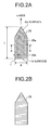
- FIG. 2A and FIG. 2B schematically show cross sections of gallium nitride crystal according to the embodiment.
- FIG. 2A and FIG. 2B illustrate cross sections parallel to the c-axis and the a-axis in the gallium nitride crystal 25 having a hexagonal crystal structure.
- the gallium nitride crystal 25 is elongated in the c-axis direction as illustrated in FIG. 2A , and has a "boron rich" region (the first region 25a) at inner side thereof and a "boron poor" region (the second region 25b) at outer side thereof.
- the gallium nitride crystal 25 may not have such a double layer structure made of the first region 25a and the second region 25b, as illustrate in FIG. 2B .
- the gallium nitride structure 25 may have a multiple layer structure more than double layers.
- the upper surface of the six-sided pyramid-like part is comprised of Ga (gallium) surface
- the bottom surface of the hexagonal column-like part is comprised of N (nitrogen) surface.
- the Ga surface and the N surface can be distinguished by comparing shapes of both edges of the needle-like crystal.
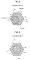
- FIG. 3 and FIG. 4 show examples of the c-plane ( ⁇ 0001 ⁇ plane) cross section of the gallium nitride crystal 25.
- FIG. 3 is a cross section along A-A line in FIG. 2A .
- the cross section orthogonal to the c-axis (c-plane) in the gallium nitride crystal 25 is a hexagon or almost hexagon.
- the surfaces of the gallium nitride crystal 25 corresponding to edges of the hexagon are comprised mainly of m-planes of the hexagonal crystal structure.
- the gallium nitride crystal 25 has preferably the boron rich region (the first region 25a) at inner side thereof in the c-plane cross section, and the boron poor region (the second region 25b) preferably surrounds at least a part of the first region 25a in the c-plane cross section.
- the gallium nitride crystal 25 in which the second region 25b surrounds at least a part of the outer periphery of the first region 25a is used as seed crystal, and the group 13 nitride crystal 27 is grown from the outer periphery of the seed crystal ( FIG. 10A ), the group 13 nitride crystal 27 grown from the second region 25b is likely to be of high quality.
- first region 25a and the second region 25b are included in the c-plane cross section.
- the embodiment is not limited to the precise c-plane cross section.
- the boron density of the first region 25a at the inner side is preferably 4 ⁇ 10 18 atms/cm 3 or more, the boron density of the second region 25b at the outer side is preferably less than 4 ⁇ 10 18 atms/cm 3 (see Examples).
- the second region 25b at the outer side preferably surrounds an entire outer periphery (i.e. all outer circumferential surfaces of the hexagonal shape comprised of generally m-planes) of the first region 25a at the inner side in a cross section intersecting the c-axis of the gallium nitride crystal 25 ( FIG. 4 ).
- FIG. 4 shows another example of the c-plane cross section of the gallium nitride crystal 25.
- the group 13 nitride crystal 27 can be grown from the second region 25b, and thereby the higher quality region can be increased in the group 13 nitride crystal 27.
- the thickness "t" ( FIG. 2A ) of the second region 25b at outer side is preferably 100 nm or more.
- melt-back of the seed crystal may arise. It is known that an amount of melt-back (melt-back amount) increases when the seed crystal has a low quality, especially the seed crystal includes an affected or damaged layer remained therein.
- the gallium nitride crystal 25 according to the embodiment has 100 nm or more thickness of the second region 25b which is a high quality crystal layer at the outer side of the crystal. Therefore, even in a case that the melt-back arises in the course of growing the seed crystal 25, the second region 25b is likely to be remained. Therefore, the group 13 nitride crystal 27 of high quality can be easily formed.
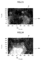
- FIG. 5 shows an example of emission spectra with electron beam or UV excitation of the first region 25a and the second region 25b (see Examples).
- the gallium nitride crystal 25 includes the first region 25a at an inner side of the cross section intersecting the c-axis of the gallium nitride crystal having the hexagonal crystal structure, and includes the second region 25b surrounding at least a part of the first region 25a in the cross section.
- the first peak including the band edge emission of GaN has the peak intensity smaller than that of the second peak which appears in longer wavelength area than the first peak.
- the first peak In emission spectrum of the second region 25b with electron beam or UV excitation, the first peak has the peak intensity greater than that of the second peak.
- the first peak refers to a peak which includes the band edge emission of GaN and which appears around about 365 nm in the measurement at a room temperature.
- the band edge emission of GaN is an emission due to a recombination of holes in an upper edge of the valence band and electrons in bottom of the conduction band in the gallium nitride crystal 25, and means that the light having energy (wavelength) equal to the band gap is emitted.
- the first peak is a peak due to a periodic structure of the crystal and a combination (status) of nitrogen and gallium in the gallium nitride crystal 25.
- the first peak may include an emission in the vicinity of the band edge in addition to the band edge emission.
- the second peak refers to at least one peak which appears in a longer wavelength area than the first peak, refers to a peak of emission spectrum due to reasons other than the band edge emission or the emission in the vicinity of the band edge of GaN, and refers to a peak due to reasons other than the combination of nitrogen and gallium.
- the second peak appears in a range from 450 nm to 650 nm with respect to an emission spectrum with electron beam or UV excitation when measured at a room temperature.
- the second peak appears in a range from 590 nm to 650 nm with respect to an emission spectrum with electron beam or UV excitation when measured at a room temperature.
- the room temperature refers to about 20 degrees Celsius, and refers to a range of about 10 degrees Celsius to 30 degrees Celsius.
- the second peak may split into a plurality of peaks.
- the second peak according to the embodiment may split into a plurality peak when measured at a temperature other than the room temperature, insofar as the second peak appears as a broad peak when measured at the room temperature.
- the emission spectra with electron beam or UV excitation can be obtained by measuring PL (Photoluminescence) using He-Cd laser (helium-cadmium laser) as exciting light source.
- PL Photoluminescence
- He-Cd laser helium-cadmium laser
- the embodiment is not limited to this. It is possible to observe colors or intensities of spectra by using fluorescence microscope.
- the first region 25a and the second region 25b can be distinguished or identified by observed colors.
- a fact that the second peak has a peak intensity greater than that of the first peak as shown in the emission spectrum of the first region 25a means that the first region 25a contains a relatively large amount of impurities or defects.
- a fact that the first peak has a peak intensity greater than that of the second peak as shown in the emission spectrum of the second region 25b means that the second region 25b contains less impurities or defects and thereby the second region 25b is a high quality crystal.
- the peak intensity of the first peak and the peak intensity of the second peak with respect to the first region 25a and second region 25b are not limited to any particular one, insofar as the aforementioned relationships are satisfied.
- the peak intensity of the first peak of the second region 25b is greater than the peak intensity of the first peak of the first region 25a.
- the peak intensity of the second peak of the second region 25b is smaller than the peak intensity of the second peak of the first region 25a.
- the second region 25b having less impurities or defects is located at an outer side in the cross section intersecting the c-axis of the gallium nitride crystal 25.
- the gallium nitride crystal 25 is not limited to the double-layered structure made of the first region 25a and the second region 25b.
- the gallium nitride crystal 25 may have a multi-layered structure more than double-layered (e.g. three-layered).
- the gallium nitride crystal 25 may include other regions different from the first region 25a and the second region 25b in its structures or properties.
- the gallium nitride crystal 25 may include a plurality of first regions or second regions.
- the gallium nitride crystal 25 may include a region whose emission spectrum with electron beam or UV excitation has a weak intensity.
- FIG. 6 schematically shows another example of the c-plane cross section of the gallium nitride crystal 25.
- the second region 25b may be made of the second region 25b1 and the second region 25b2.
- the first peak of the second region 25b2 has a peak intensity smaller than that of the first peak of the second region 25b1.
- the second region 25b2 may be formed so as to surround the first region 25a or the second region 25b1.
- Additives may be doped to the gallium nitride crystal 25 (the first region 25a and the second region 25b) according to the embodiment.
- Additives may be a doping impurity such as germanium (Ge), oxygen (O), silicon (Si) and the like, an acceptor impurity such as magnesium (Mg), lithium (Li), strontium (Sr), calcium (Ca), zinc (Zn) and so on, a transition metal for providing magnetic property such as iron (Fe), manganese (Mn), chromium (Cr) and the like, a rare earth element or the like for providing magnetic property or fluorescence such as europium (Eu), erbium (Er), terbium (Tb), thulium (Tm) and the like, congeners such as aluminum (Al), indium (In) and the like.
- Other additives may de selected and doped depending on the purpose.
- the c-plane cross section of the gallium nitride crystal 25, the c-plane cross section of the first region 25a, and the c-plane cross section of the second region 25b are illustrated as regular hexagon, respectively. However, these drawings are only for illustrating examples.
- the c-plane cross section is not limited to the regular hexagon.
- the c-plane cross section of the gallium nitride crystal 25, the c-plane cross section of the first region 25a, and the c-plane cross section of the second region 25b are formed in generally hexagon due to the cross section of the gallium nitride crystal having a hexagonal crystal structure. In a case that other structure arises inside or at a boundary of these cross section in the course of the crystal growth, the outline of each hexagon may deform at the boundary with other structure.
- the manufacturing method of crystal according to the embodiment is a method of manufacturing a group 13 nitride crystal (e.g. gallium nitride crystal) by a flux method in which the gallium nitride crystal 25 mentioned in [2] is used as a seed crystal (seed crystal 25) and the c-plane cross section of the seed crystal 25 is enlarged.
- a group 13 nitride crystal e.g. gallium nitride crystal
- FIG. 7 schematically shows a crystal manufacturing apparatus 2 to grow a seed crystal 25.
- the apparatus 2 has a double vessel structure in which an inner vessel 51 is disposed in an outside pressure resistant vessel 50 made of stainless material, and a reactor vessel 52 is disposed in the inner vessel 51.
- the inner vessel 51 is attachable to and detachable from the outside pressure resistant vessel 50.
- the reactor vessel 52 is for maintaining the seed crystal 25 with a molten mixture 24 of alkali metal and group 13 element-contained material in order to grow the seed crystal 25 (to grow the bulk crystal from seed crystal is referred to as SG or Seed Growth).
- Materials for the reactor vessel 52 are not limited to any particular material.
- nitrides such as sintered BN, P-BN and the like, oxides such as aluminum, YAG and the like, carbides such as SiC and the like, and so on may be used.
- An inner wall of the reactor vessel 52, that is, a portion or portions of the reactor vessel 52 which contact(s) the molten mixture 24 is/are preferably made of material(s) insensitive to the molten mixture 24.
- nitrides such as boron nitride (BN), pyrolytic BN (P-BN), aluminum nitride and the like, oxides such as alumina, yttrium-aluminum-garnet (YAG) and the like, stainless steel (SUS) and so on.
- gas pipes 65 and 66 are respectively connected to supply nitrogen (N 2 ) gas which is source material of the group 13 nitride crystal and a diluent gas for controlling a whole pressure to an inner space 67 of the outside vessel 50 and an inner space 68 of the inner vessel 51.
- a gas supplying pipe 54 is branched into a nitrogen supplying pipe 57 and a diluent gas supplying pipe 60 via valves 55 and 58, respectively. These pipes 57 and 60 can be separated at valves 55 and 58, respectively.
- Argon (Ar) gas which is inert gas is preferably used as the diluent gas.
- other inert gas such as helium (He) may be used as the diluent gas.
- the nitrogen gas is introduced from the nitrogen supplying pipe 57 which is connected to a gas canister or the like containing the nitrogen gas therein.
- the nitrogen gas from the pipe 57 is subjected to a pressure control by a pressure regulator 56 and then supplied to the gas supplying pipe 54 via the valve 55.
- the diluent gas e.g. Ar gas
- the diluent gas from the pipe 60 is introduced from the diluent gas supplying pipe 60 which is connected to a gas canister or the like containing the diluent gas therein.
- the diluent gas from the pipe 60 is subjected to a pressure control by a pressure regulator 59 and then supplied to the gas supplying pipe 54 via the valve 58.
- the pressure regulated nitrogen gas and the pressure regulated diluent gas are supplied to the gas pipe 54 to be mixed there.
- the gas mixture of the nitrogen gas and the diluent gas is supplied to the outside vessel 50 via the pipe 65 and the inner vessel 51 via the pipe 66.
- the inner vessel 51 can be removed from the apparatus 2 at the valve 61.
- a pressure meter 64 is disposed on the pipe 54 for monitoring a whole pressure inside of the outside vessel 50 and the inner vessel 51 and controlling pressures inside of the outside vessel 50 and inner vessel 51.
- nitrogen partial pressure can be controlled by controlling the pressures of the nitrogen gas and the diluent gas by means of valves 55 and 58 and the pressure regulators 56 and 59. Since the whole pressure of the outside vessel 50 and the inner vessel 51 can be controlled, it is possible to reduce evaporation of alkali metal (e.g. sodium) in the reactor vessel 52 by increasing the whole pressure of the inner vessel 51. In other words, it is possible to control separately the nitrogen partial pressure which becomes a nitrogen source affecting the crystal growth conditions of GaN and the whole pressure which affects the reduction of sodium evaporation.
- alkali metal e.g. sodium
- a heater 53 is disposed around the outer circumference of the inner vessel 51 inside of the outside vessel 50 for heating the inner vessel 51 and the reactor vessel 52 and controlling the temperature of the molten mixture 24.
- An operation to put the seed crystal 25, the source material, the flux material, additives and the like such as gallium (Ga), sodium (Na), and carbon (C) as dopant into the reactor vessel 52 is conducted in such a manner that the inner vessel 51 is put into a glove box under an inert gas atmosphere such as Ar. This operation may be conducted in a state that the reactor vessel 52 is set inside of the inner vessel 51.
- the seed crystal 25 mentioned in [2] is set or installed (the seed crystal installation process).
- FIG. 8 and FIG. 9 schematically illustrate examples of ways of installing the seed crystal 25 (showing in section).
- a hole (recess) having an inner diameter larger than an outer diameter of the seed crystal 25 is made in a bottom part of the reactor vessel 52.
- the seed crystal 25 is installed by inserting an edge of the seed crystal 25 into the hole (recess).
- the seed crystal 25 is installed in the reactor vessel 52 so that Ga surface faces upward, as shown in FIG. 8 .
- the seed crystal 25 is installed in the rector vessel 52 so that N surface faces upward, as shown in FIG. 9 .
- the seed crystal 25 is installed by inserting it into the hole or recess.
- the installation method is not limited to this. Other installation method may be used.
- the seed crystal 25 to be installed inside the reactor vessel 52 is a gallium nitride crystal 25 having a hexagonal crystal structure in which a length in the c-axis direction is 9.7 mm or more, and the ratio L/d of the length "L" to the crystal diameter "d" in the c-plane is larger than 0.813.
- Material used as flux may be sodium or compound thereof (e.g. sodium azide). Other alkali metals such as lithium, potassium and the like, or compounds of these alkali metals may be used as flux. Alkali earth metals such as barium, strontium, magnesium and the like, or compounds of these alkali earth metals may be used as flux. Plurality kinds of alkali metals or alkali earth metals may be used.
- the material containing group 13 element as source material may be gallium which is one of group 13 elements. Any other materials including without limitation other group 13 elements such as boron, aluminum and indium, or mixtures thereof may be used as source material(s).
- a mol ratio of the material containing or including the group 13 element to alkali metal is not limited to any particular one. However, the mol ratio of alkali metal to the total mol ratio of the alkali metal and the group 13 element is preferably 40 % to 95 %.
- the heater 53 is turned on to heat the inner vessel 51 and the reactor vessel 52 inside of the inner vessel 51 to a crystal growth temperature. Then, the source materials in the reactor vessel 52, which are the material containing or including group 13 element, alkali metal, and other additives, are melted in the reactor vessel 52 to form the molten mixture 24 (the molten mixture forming process).
- the nitrogen which is a source material of the group 13 nitride crystal 27 can be supplied to the molten mixture 24 (the nitrogen dissolving process).
- Source materials melted in the molten mixture 24 are supplied onto the outer circumference surface of the seed crystal 25, so that the group 13 nitride crystal 27 is grown from the outer circumference surface of the seed crystal 25 with the source materials.
- the group 13 nitride crystal 27 is grown from the seed crystal 25 with the source materials.
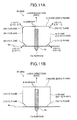
- FIG. 10A, FIG. 10B , FIG. 11A and FIG. 11B illustrate the growth processes and crystal shapes of the group 13 nitride crystal 80.
- a preferable crystal growth process includes a process of forming an outer side periphery mainly including ⁇ 10-10 ⁇ plane and an outer side periphery mainly including ⁇ 10-11 ⁇ plane at the sides of the crystal, and forming an outer periphery mainly including ⁇ 0001 ⁇ plane at the bottom of the crystal (see Example 1).
- a preferable crystal growth process includes a process of forming outer peripheries mainly including ⁇ 0001 ⁇ plane at the top face and the bottom face of the crystal, and forming an outer side periphery mainly including ⁇ 10-10 ⁇ plane and an outer side periphery mainly including ⁇ 10-11 ⁇ plane at the sides of the crystal (see Example 2).
- a growth rate in ⁇ 10-10> direction (the m-axis direction) is the fastest in the crystal growth rate of the group 13 nitride crystal 27.
- the growth rate in [0001] direction (the c-axis direction at Ga surface side), and the growth rate in ⁇ 10-11> direction having Ga surface side component follows.
- the growth rate in [000-1] direction (the c-axis direction at N surface side), and the growth rate in ⁇ 10-11> direction having N surface side component are slow in comparison with the other growth rates.
- the ⁇ 10-11> direction having Ga surface side component means a direction in which the value "1" of hexagonal crystal index [hkil] has a positive value in the ⁇ 10-11> direction.
- [10-11] direction and [-1011] direction are illustrated in FIG. 11A .
- the ⁇ 10-11> direction having N surface side component means a direction in which the value "1" of hexagonal crystal index [hkil] has a negative value in the ⁇ 10-11> direction.
- [10-1-1] direction and [-101-1] direction are illustrated in FIG. 11A .
- the growth rate in [0001] direction, the growth rate in ⁇ 10-10> direction and the growth rate in ⁇ 10-11> direction having Ga surface side component are relatively fast.
- the group 13 nitride crystal 27 is likely to be formed into a shape as illustrated in FIG. 10A or FIG. 10B .
- the crystal is likely to be formed into a shape as illustrated in FIG. 10A .
- the growth rate in ⁇ 10-11> direction having Ga surface side component is slower than the growth rate in [0001] direction, the crystal is likely to be formed into a shape as illustrated in FIG. 10B .
- the growth rate in a direction at N surface side that is, the growth rate in [000-1] direction and the growth rate in ⁇ 10-11> direction having N surface side component are slower than the growth rate in ⁇ 10-10> direction.
- the group 13 nitride crystal 27 is likely to be formed into shapes as illustrated by FIG. 11A and FIG. 11B .
- the crystal is likely to be formed into a shape as illustrated in FIG. 11A .
- the growth rate in ⁇ 10-11> direction having N surface side surface component is slower than the growth rate in [000-1] direction, the crystal is likely to be formed into a shape as illustrated in FIG. 11B .
- the group 13 nitride crystal 27 are illustrated with growth striations 71 which appears in accordance with the crystal growth. However, the group 13 nitride crystal 27 may or may not have the growth striation 71.
- the gallium nitride crystal 25 having a hexagonal crystal structure in which the length "L” in the c-axis direction is 9.7 mm or more, and the ratio L/d of the length "L” to the crystal diameter "d" is larger than 0.813 is used as seed crystal, and the group 13 nitride crystal 27 having a hexagonal crystal structure is grown to form the group 13 nitride crystal 80.
- the group 13 nitride crystal 80 By forming the group 13 nitride crystal 80 from the seed crystal 25 having such a shape, a crystal substrate can be fabricated with high quality and practical size. The detail about this will be described later in the following [7] and ]8].
- the partial pressure of nitrogen gas in the inner space 68 of the inner vessel 51 and the inner space 67 of the outer pressure resistant vessel 50 is at least 0.1 MPa or more. In a more preferred embodiment, the partial pressure of nitrogen gas in the inner space 68 of the inner vessel 51 and the inner space 67 of the outer pressure resistant vessel 50 is in a range of 2 MPa to 5 MPa.
- the temperature of the molten mixture 24 (the crystal growth temperature) is at least 700 degrees Celsius or more. In a more preferred embodiment, the crystal growth temperature is in a range of 850 degrees Celsius to 900 degrees Celsius.
- the dislocation density of the group 13 nitride crystal 27 grown mainly from the outer periphery comprised of m-planes of the seed crystal 25 is considered to be affected by the quality of the outer periphery comprised of m-planes of the seed crystal 25.
- the outer periphery comprised of m-planes of the seed crystal 25 is of high quality with low dislocation density.
- the same material e.g. gallium nitride
- the group 13 nitride crystal 27 grown from the seed crystal 25 may be used for the seed crystal 25 and the group 13 nitride crystal 27 grown from the seed crystal 25. Therefore, different from a case that hetero material such as aluminum nitride (AlN) is used as the seed crystal, the lattice constant and the thermal expansion coefficient can be matched and thereby the occurrence of the dislocation due to the difference in the lattice constant or thermal expansion coefficient can be suppressed.
- AlN aluminum nitride
- the seed crystal 25 and the group 13 nitride crystal 27 are manufactured by the same or similar crystal manufacturing method (flux method). Therefore, in comparison with a case that the seed crystal 25 and the group 13 nitride crystal 27 are manufactured by the different method from each other, it is possible to improve the matching of the lattice constant or the thermal expansion coefficient, and thereby easily suppress the occurrence of dislocation.
- the crystal manufacturing method of embodiment it is possible to manufacture the group 13 nitride crystal 80 of high quality with low dislocation density and of practical size.
- the explanation was focused on the flux method for the crystal manufacturing method.
- the crystal manufacturing method is not limited to any particular one.
- a vapor phase growth method such as HVPE, or any other liquid phase growth method than flux method may be used for the crystal growth.
- the group 13 nitride crystal according to the embodiment is a group 13 nitride crystal 80 manufactured by the manufacturing method as mentioned in [3]. Therefore, the group 13 nitride crystal 80 according to the embodiment includes, at the inner side thereof, at least a part of the gallium nitride crystal 25 mentioned in [2].
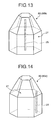
- FIG. 12 and FIG. 13 show perspective views or appearances of group 13 nitride crystals 80 (80a and 80b) according to the embodiment. As illustrated in FIG. 12 and FIG. 13 , the seed crystals 25 are contained in the group 13 nitride crystal 80a ( FIG. 12 ) and the group 13 nitride crystal 80b ( FIG. 13 ).
- FIG. 14 shows a perspective view or appearance of another example of the group 13 nitride crystal 80c.
- the seed crystal 25 is located inside of the group 13 nitride crystal 80.
- the seed crystal 25 maybe located around the center (around the center of the hexagonal cross section) of the group 13 nitride crystals 80a and 80b, as shown in FIG. 12 and FIG. 13 .
- the seed crystal 25 may be located around the periphery (in an area closer to edges of the hexagon than the center) of the group 13 nitride crystal 80c, as shown in FIG. 14 .
- the group 13 nitride crystal 80 may have a shape further enlarged to the m-axis direction.
- additives may be doped in the group 13 nitride crystal 27.
- additives include a doping impurity such as germanium (Ge), oxygen (O), silicon (Si) and the like, an acceptor impurity such as magnesium (Mg), lithium (Li), strontium (Sr), calcium (Ca), zinc (Zn) and the like, a transition metal for providing magnetic property such as iron (Fe), manganese (Mn), chromium (Cr) and the like, a rare earth element or the like for providing magnetic property or fluorescence such as europium (Eu), erbium (Er), terbium (Tb), thulium (Tm) and the like, congeners such as aluminum (Al), indium (In) and the like.
- Other additives may de selected and doped depending on the purpose.
- the group 13 nitride crystal 27 grown from the seed crystal and the gallium nitride crustal 25 used as the seed crystal can be of the same gallium nitride.
- the lattice constant or thermal expansion coefficient can be matched, and thereby the occurrence of the dislocation due to the difference in the lattice constant or the thermal expansion coefficient can be suppressed.
- the second region 25b having less impurities or defects is disposed at outer side in the cross section intersecting the c-axis of the gallium nitride crystal 25.
- the high quality group 13 nitride crystal 27 can be manufactured when the group 13 nitride crystal 27 is grown from the gallium nitride crystal 25 as seed crystal. Namely, it is further possible to suppress the dislocation which may occur at a boundary surface of the gallium nitride crystal 25 used as seed crystal.
- FIG. 15 schematically shows dislocations in a cross section parallel to the c-axis and the a-axis in the group 13 nitride crystal 80.
- FIG. 15 only shows an enlarged right part from the seed crystal 25 in a a-plane cross section of the group 13 nitride crystal 80.
- the group 13 nitride crystal 27 grown from the seed crystal 25 is grown mainly from m-planes comprising the outer periphery of the seed crystal 25 toward the m-axis direction (i.e. a direction in which the c-plane cross section of the hexagon enlarges). Therefore, the dislocations occurred at the growth boundary surface of the seed crystal 25 are likely to be oriented in ⁇ 11-20> direction parallel to the crystal growth direction and are not likely to be oriented in ⁇ 11-23> direction unparallel to the crystal growth direction.
- dislocation direction intersecting the c-plane cross section of the group 13 nitride crystal having a hexagonal crystal structure there are ⁇ 0001> direction and ⁇ 11-23> direction. In the embodiment, however, the dislocation in the ⁇ 0001> direction does not occur and the dislocation in the ⁇ 11-23> direction occurs quite a few.
- the dislocation density of the group 13 nitride crystal 27 (a region other than the seed crystal 25 in the group 13 nitride crystal 80) is smaller than that of the gallium nitride crystal 25 contained inside of the group 13 nitride crystal 27.
- the fabrication method of the crystal substrate according to the embodiment is a method of fabricating the crystal substrate 100 from the group 13 nitride crystal 80 mentioned in [4].
- FIG. 16 and FIG. 17 schematically show direction for slicing the group 13 nitride crystal 80b ( FIG. 13 ) and the group 13 nitride crystal 80c ( FIG. 14 ).
- FIGs. 18A to 18C , and FIGs. 19A to 19C schematically show examples of crystal substrate 100 (100a to 100f) obtained through slicing.
- the fabrication method according to the embodiment includes a process of cutting out the crystal substrate 100 so as to include at least a part of the seed crystal 25 when the group 13 nitride crystal 80 is sliced.
- the crystal substrate 100a as shown in FIG. 18A can be obtained by cutting or slicing the crystal 80 orthogonal to the c-axis of the seed crystal 25 as shown by a dotted-dashed line P1 in FIG. 16 .
- the crystal substrate 100b as shown in FIG. 18B can be obtained by cutting or slicing the crystal 80 oblique to the c-axis of the seed crystal 25 as shown by a dotted-dashed line P2 in FIG. 16 .
- the crystal substrate 100c as shown in FIG. 18C can be obtained by cutting or slicing the crystal 80 along the c-axis of the seed crystal 25 as shown by a dotted-dashed line P3 in FIG. 16 .
- the crystal substrate 100 as shown in FIGs. 18a to 18C and FIGs. 19A to 19C (100a to 100f can be obtained through various treatments such as forming or shaping process, surface treatment and the like after slicing.
- the fabrication method of the embodiment it is possible to obtain a large area of main face of the substrate, since the crystal substrate 100 is cut out from the group 13 nitride crystal 80 enlarged in the c-axis direction as mentioned above, whether the substrate is cut out along the c-plane or along a plane other than the c-plane.
- the crystal substrate 100 having a large area and a main face comprised of any crystal plane such as c-plane, m-plane, a-plane, ⁇ 10-11 ⁇ plane, ⁇ 20-21 ⁇ plane, ⁇ 11-22 ⁇ plane and so on. Therefore, it is possible to fabricate the crystal substrate 100 of practical size applicable to various semiconductor devices.
- the crystal substrate 100 is fabricated by slicing the bulk crystal of the group 13 nitride (the group 13 nitride crystals 80 to 83).
- the method does not include a process of separating a thick crystal film from the hetero material substrate on which the crystal is grown and which has a thermal expansion coefficient and a lattice constant considerably different from that of the crystal thereon. Thereby, cracks hardly occur in the crystal substrate 100 according to the fabrication method of the embodiment. Therefore, it is possible to fabricate the crystal substrate 100 of higher quality in comparison with the prior art.
- the crystal substrate according to the embodiment is a crystal substrate 100 fabricated by the fabrication method mentioned in [5].
- the crystal substrate 100 of the embodiment characteristically includes at least a part of the seed crystal 25 mentioned in [2].
- the seed crystal 25 used in the crystal manufacturing process mentioned in [3] is included in the crystal substrate 100 of the embodiments (100a to 100f). At least a part of the outer periphery comprised of m-planes of the seed crystal 25 is surrounded by the group 13 nitride crystal 27 grown from the seed crystal 25.
- an entire outer periphery comprised of m-planes of the seed crystal 25 is surrounded by the group 13 nitride crystal 27.
- the position thereof is not limited to any particular one.
- the seed crystal 25 may be disposed around the center part of the main face of the crystal substrate 100.
- the c-axis of the seed crystal 25 may be disposed perpendicular to the main face as shown in FIG. 18A , or may be disposed oblique to the main face as shown in FIG. 18B .
- the seed crystal 25 may be disposed so that the c-axis of the seed crystal 25 is parallel to the main face of the substrate. Furthermore, the seed crystal 25 may be disposed at a position other than the center area of the main face of the substrate 100. For example, as shown in FIG. 19A and FIG. 19B , the seed crystal 25 may be disposed near the periphery of the main face of the substrate 100.
- the c-plane of the hexagonal crystal structure becomes a main face of the crystal substrate 100.
- the dislocation extending through the c-plane (line defect) is likely to be reduced in the group 13 nitride crystal 27 in a preferred embodiment. Therefore, when the crystal substrate 100 having a main face comprised of c-plane is fabricated from the group 13 nitride crystal 80, the line defect extending in the c-axis direction can be reduced and a high quality crystal substrate 100 can be obtained.
- FIG. 20A and FIG. 20B schematically show examples of the crystal growth of the group 13 nitride crystal 27 from the seed crystal 25.
- a m-plane cross section of the group 13 nitride crystal 80 is illustrated in FIG. 20A and FIG. 20B , respectively.
- the group 13 nitride crystal 27 grown from the seed crystal 25 includes a region 27a and a region 27b.
- the region 27a is grown mainly toward the m-axis direction (i.e. a direction in which the c-plane cross section of the hexagon enlarges) from the m-plane comprising the outer periphery of the seed crystal 25.
- the region 27 b is grown mainly from a slanted surface including ⁇ 10-11 ⁇ plane of the seed crystal 25 or from a slanted surface including ⁇ 10-11 ⁇ plane on the top of the region 27a toward ⁇ 10-11> direction.
- the growth rate of forming ⁇ 10-11 ⁇ plane is considered to be the slowest or rate controlling.
- the group 13 nitride crystal 27 grown around the upper part of the seed crystal 25 is considered to often become a six-sided pyramid-like shape as shown in FIG. 20A .
- the upper part of the crystal 27 may be a truncated six-sided pyramid-like shape in which a top part of the pyramid is cut along the c-plane.
- FIG. 21A and FIG. 21B schematically show examples of the crystal growth when the length "L" ( FIG. 2A ) in the c-axis direction of the seed crystal 25 is short.
- the length "L" of the seed crystal 25 is not long enough, the ratio of the six-sided pyramid part to the hexagonal column-like part is large. Therefore, the region 27b grown toward the ⁇ 10-11> direction has a larger volume ratio to the region 27a grown toward the m-axis direction. Therefore, the group 13 nitride crystals 90, 91 are likely to be shapes illustrated FIG. 21A and FIG. 21B . In these cases, the region 27b is included all the c-planes.
- the region 27a is a region whose crystal growth is started from the outer periphery comprised of m-planes of the seed crystal 25.
- the group 13 nitride crystal 27 (the region 27a) grown mainly from the m-planes of the seed crystal 25 is considered to have relatively less dislocation extending through the c-axis direction. Therefore, when the crystal substrate 100 (100a, 100b, 100d, 100e) whose main face is a c-plane is fabricated, the region 27a is preferably contained or included as much as possible.
- the crystal substrate 100 is fabricated by using a lower par of the group 13 nitride crystal 80, that is, a hexagonal column-like part without including the region 27b, it is possible to obtain the crystal substrate 100 including no region 27b considered to be grown from planes other than m-planes.
- the obtained substrate 100 includes both the region 27a and the region 27b.
- regions grown toward different directions often have different properties from each other.
- the seed crystal and the crystal grown from the seed crystal often have different properties. Therefore, the substrate 100 fabricated from the crystal 90 or 91 as shown in FIG. 21A or 21B has three regions, that is, the regions 27a and 27b, and the seed crystal 25. This may lower the quality of the substrate 100.
- the group 13 nitride crystal 80 is of a shape including a hexagonal column-like part at the lower part of the crystal.
- the preferred shape is not limited to examples of FIG. 20A and FIG. 20B .
- the group 13 nitride crystal may grow from the seed crystal 25 mainly toward the m-axis direction and mainly have a hexagonal column-like shape.
- the gallium nitride crystal 25 has a hexagonal crystal shape in which an angle formed between the "a+c"-axis ( ⁇ 11-23> direction) and the c-plane is 58.4 degrees. If the ratio L/d of the length "L" ( FIG. 2A ) in the c-axis direction of the gallium nitride crystal 25 to the crystal diameter "d" in the c-plane cross section is 0.813, the gallium nitride crystal 25 becomes a six-sided pyramid-like shape.
- the group 13 nitride crystal 27 is preferably grown mainly from the outer surface comprised of m-planes of the seed crystal 25.
- the seed crystal 25 includes m-planes as the outer periphery.
- FIG. 22 schematically shows various relationships between the ratio L/d and the shape of the seed crystal 25.
- the seed crystal 25 becomes a six-sided pyramid-like shape.
- the ratio L/d is greater than 0.813 (L/d>0.813)
- the upper part becomes a six-sided pyramid-like shape and the lower part becomes a hexagonal column-like shape.
- the outer periphery (side surfaces) of the seed crystal 25 includes m-planes.
- the seed crystal 25 becomes a six-sided pyramid-like shape without including any m-plane, or becomes a shape having a truncated six-sided pyramid-like part without a top part of the pyramid and having a low profile hexagonal column-like part including the m-planes.
- the ratio L/d is greater than 0.813 in the seed crystal 25, in which "L" is the length in the c-axis direction and d is a crystal diameter in the c-plane.
- the practical size of the crystal substrate 100 is preferably a half-inch (12.7 mm) or 2 inches (5.08 cm).
- the explanation will be made on the size of the seed crystal 25 required in a case that group 13 nitride crystal substrate 100 having the c-plane as main face has a diameter of half-inch (12.7 mm) or more, or a diameter of 2 inches or more is to be fabricated.
- the required minimum thickness is not limited to this, and can be simulated as appropriate.
- the group 13 nitride crystal 27 is required to be grown to a radius direction (the m-axis direction) by 6.35 mm, if the diameter of the seed crystal 25 is neglected as zero.
- the crystal growth rate Vm in the m-axis direction is assumed to be twice of the crystal growth rate Vc in the c-axis direction, the crystal is grown about 3.2 mm in the c-axis direction while grown 6.35 mm in the m-axis direction.
- the minimum length of the seed crystal 25 required for obtaining the group 13 nitride crystal 80 having the six-sided pyramid-like shape as shown in FIG. 20 is 8.7 mm. It is desired that a hexagonal column-liked region is formed under the six-sided pyramid-like part. If the required thickness of the crystal substrate 100 is assumed as 1 mm or more, the required length "L" in the c-axis direction of the seed crystal 25 is estimated as 9.7 mm.
- the length "L" in the c-axis direction of the seed crystal 25 is preferably 9.7 mm or more.
- the ratio L/d (the ratio of the length "L” in the c-axis direction to the diameter d in the c-plane) is preferably greater than 0.813, and the length "L" is preferably 9.7 mm or more. More preferably, L/d is greater than 7, and still more preferably, L/d is greater than 30.
- the crystal substrate 100 having the diameter of the c-plane that is half-inch.
- the group 13 nitride crystal 80 grown from the m-plane of the seed crystal 25 is of high quality, a large and high quality crystal substrate 100 can be fabricated.
- the required length "L" in the c-axis direction of the seed crystal 25 is estimated as 37.4 mm or more.
- the length "L" in the c-axis direction of the seed crystal 25 is preferably 37.4 mm or more. Thereby, it is possible to fabricate the crystal substrate 100 having the diameter in the c-plane that is 2 inches. As mentioned above, since the group 13 nitride crystal 80 grown from the m-plane of the seed crystal 25 is of high quality, a large diameter and high quality crystal substrate 100 of the gallium nitride can be fabricated.
- the seed crystal 25 was manufactured by using the crystal manufacturing apparatus 1 illustrated in FIG. 1 . Reference numerals in the following explanation correspond to the construction of the apparatus 1 explained with reference to FIG. 1 .
- gallium having the nominal purity of 99.99999 % and sodium having the nominal purity of 99.95 % were input with a mol ratio as 0.25:0.75 into the reactor vessel 12 made of a sintered BN and having the inner diameter of 92 mm.
- the reactor vessel 12 was placed into the inner vessel 11 under a high purity Ar gas atmosphere.
- the valve 31 was closed to shut out the inner space of the reactor vessel 12 from the outer atmosphere, so that the inner vessel 11 was sealed under the state filled with Ar gas.
- the inner vessel 11 was taken out from the glove box and then assembled into the crystal manufacturing apparatus 1.
- the inner vessel 11 I was installed at a predetermined position with respect to the heater 13 and connected to the gas supplying pipe 14 of nitrogen gas and argon gas at the valve 31 portion.
- the nitrogen gas was introduced from the nitrogen supplying pipe 17.
- the nitrogen gas was subjected to the pressure control by the pressure regulator 16, and the valve 15 was opened, so that the nitrogen pressure in the inner vessel 11 was 3.2 MPa.
- the valve 15 was closed and the pressure regulator 16 was set at 8 MPa.
- the heater 13 was turned on to heat the reactor vessel 12 to a crystal growth temperature. In this Example, the crystal growth temperature was 870 degrees Celsius.
- gallium and sodium in the reactor vessel 12 were melted to form a molten mixture 24.
- the temperature of the molten mixture 24 was the same as the temperature of the reactor vessel 12. Until heated to this temperature, in the crystal manufacturing apparatus 1 of this Example, gas in the inner vessel 11 was heated so that the whole pressure was 8 MPa.
- valve 15 was opened so that the pressure of nitrogen gas was 8 MPa, and the pressure equilibrium state was established between the inside of the inner vessel 11 and the inside of the nitrogen supplying pipe 17.
- gallium nitride crystals 25 were formed. Grown gallium nitride crystals 25 were colorless and transparent, had the crystal diameter "d" of about 100 to 1500 ⁇ m, had the length "L” of about 10 to 40 mm, and had the ratio L/d of the length "L” to the crystal diameter d was about 20 to 300. The gallium nitride crystals 25 were grown generally parallel to the c-axis, and had the m-planes (see FIG. 3 ) formed on the side surfaces of each crystal.
- the gallium nitride crystal 25 manufactured in this Example was subject to various measurements. The measurement results were shown below.
- Photoluminescence (PL) was measured at a room temperature (25 degrees Celsius) with respect to the gallium nitride crystal manufactured in the Example. Photoluminescence was measured by using LabRAM HR-800 fabricated by HORIBA, Ltd. As an exciting light source, helium-cadmium (He-Cd) laser having a wavelength of 325 nm was used. Photoluminescence was measured with respect to the first region 25a which was an inner region of the seed crystal 25 and with respect to the second region 25b which was an outer region of the seed crystal 25, respectively.
- He-Cd helium-cadmium
- FIG. 5 shows one example of measurement result of emission spectra of PL with respect to the first region 25a and the second region 25b.
- the horizontal axis means wavelength (nm), and the vertical axis means emission intensity.
- a broad emission (the second peak) having a peak around 600 nm was observed in a range of 500 nm to 800 nm, while only a very weak intensity of emission was observed for an emission (the first peak) from a vicinity of band edge (365 nm) of gallium nitride.
- the peak intensity of the first peak was smaller than the peak intensity of the second peak in the first region 25a contained at inner side of the seed crystal 25. It was also confirmed that the peak intensity of the first peak was greater than the peak intensity of the second peak in the second region 25b located at outer side of the seed crystal 25.
- FIG. 23 and FIG. 24 show one example of photoluminescence measurement result which was measured as for the c-plane of the gallium nitride crystal 25 manufactured by the Example, showing spectral intensity with different wavelength band at the same measurement point on the c-plane cross section.
- FIG. 23 shows a mapping image of the spectral intensity in a range of 360 nm to 370 nm of photoluminescence. Darker color indicates stronger spectral intensity in a range of 360 nm to 370 nm.
- FIG. 24 shows a mapping image of the spectral intensity in a range of 500 nm to 800 nm of photoluminescence. Darker color indicates stronger spectral intensity in a range of 500 nm to 800 nm.
- the gallium nitride crystal 25 had the first region 25a at inner side thereof and the second region 25b at outer side thereof.
- the second region 25b surrounds a whole outer periphery of the first region 25a in some gallium nitride crystals 25, as shown in FIG. 4 .
- the second region 25b surrounds a part of the outer periphery of the first region 25a, as shown in FIG. 3 .
- the second region 25b surrounds at least a part of the outer periphery of the first region 25a, in the c-plane cross section of the gallium nitride crystal 25 manufactured by the Example.
- Boron density in the crystal was measured by using a secondary ion mass spectrometer (SIMS) with respect to the gallium nitride crystal 25 manufactured by the Example.
- SIMS IMS 7f (model name) fabricated by CAMECA was used.
- primary ion beam Cs + ion was used.
- the primary ion accelerating voltage was 15 kV, and the detection area was 30 ⁇ m ⁇ .
- the boron density was measured at a plurality of points with respect to the inner region (i.e. the first region 25a) and with respect to the outer region (i.e. the second region 25b) in the c-plane cross section of the gallium nitride crystal 25, respectively, as shown in FIG. 4 .
- the boron density in the first region 25a was approximately 5 ⁇ 10 18 cm -3 to 3 ⁇ 10 19 cm -3
- the boron density in the second region 25b was approximately 1 ⁇ 10 16 cm -3 to 8 ⁇ 10 17 cm -3 .
- the gallium nitride crystal 25 manufactured by the Example it was confirmed that the boron density in the second region 25b at outer side was lower than that of the first region 25a at inner side in the c-plane cross section. Thus, it was confirmed that there was a double layered structure made of the first region 25a and the second region 25b.
- a group 13 nitride crystals 80 having a structure as shown in FIG. 10A was formed by growing the seed crystal 25 in the crystal manufacturing apparatus 2 as illustrated in FIG. 7 .
- the gallium nitride crystal having a width of 1 mm and a length of 40 mm was used as the seed crystal 25.
- the seed crystal 25 used in this Example had a structure in which the second region 25b surrounds an entire periphery of the first region 25a, as shown in FIG. 4 , in at least a part of the c-planes.
- the thickness "t" the thickness in the m-axis direction, see FIG. 2A ) of the second region 25b was at least 10 ⁇ m or more.
- the inner vessel 51 was separated from the crystal manufacturing apparatus 2 at the valve 61 portion, and placed into the glove box under Ar atmosphere.
- the seed crystal 25 was placed in the reactor vessel 52 made of alumina and having an inner diameter of 140 mm and a depth of 100 mm.
- the seed crystal 25 was retained by inserting the crystal 25 into a hole having a depth of 4 mm made at the bottom of the reactor vessel 52.
- the seed crystal 25 was retained so that Ga surface faced upward, as shown in FIG. 8 .
- the reactor vessel 52 was placed into the inner vessel 51 under a high purity Ar gas atmosphere. Then, the valve 61 was closed to seal the inner vessel 51 filled with Ar gas, and shut out the inner space of the reactor vessel 52 from the outside atmosphere. Next, the inner vessel 51 was taken out from the glove box and then assembled into the crystal manufacturing apparatus 2. Specifically, the inner vessel 51 was installed at a predetermined place with respect to the heater 53, and connected to the gas supplying pipe 54 at the valve 61 portion.
- the heater 53 was turned on to heat the reactor vessel 52 to a crystal growth temperature.
- the crystal growth temperature was 870 degrees Celsius.
- the valve 55 was opened so that the nitrogen gas pressure became 3 MPa.
- Gallium nitride crystal 27 was formed by maintaining the reactor vessel 52 for 1300 hours under this state.
- a gallium nitride crystal 80a (single crystal) having a larger crystal diameter increased in a direction orthogonal to the c-axis was formed from the gallium nitride crystal 25 as the seed crystal.
- the gallium nitride crystal 80a was generally colorless and transparent, and had the crystal diameter "d" of 51 mm, the length "L" in the c-axis direction of 54 mm including the seed crystal part 25 which were inserted into the hole at the bottom of the reactor vessel 52.
- the gallium nitride crystal 80a had a shape in which the upper part was a six-sided pyramid-like shape and the lower part was a hexagonal column-like shape, as shown in FIG. 10A .
- the outer periphery mainly made of ⁇ 10-11 ⁇ planes was formed.
- the outer periphery mainly made of m-planes ( ⁇ 10-10 ⁇ planes) was formed.
- Example 1 in which the seed crystal 25 was installed in the reactor vessel 52 so that Ga surface faced upward as shown in FIG. 8 , it was confirmed that at the upper part of the crystal, the outer periphery mainly made of ⁇ 10-10 ⁇ plane and the outer periphery mainly made of ⁇ 10-11 ⁇ plane were formed, and at the bottom surface of the crystal, the outer periphery mainly made of ⁇ 0001 ⁇ plane was formed in the obtained gallium nitride crystal 80a.
- a gallium nitride crystal 80e was formed under the same conditions of Example 1 except that the seed crystal 25 was installed in the reactor vessel 52 so that N surface side faced upward, as shown in FIG. 9 .
- the gallium nitride crystal 25 used as the seed crystal in this Example had a diameter of 1.2 mm and a length of about 50 mm.
- a gallium nitride crystal 80e having a larger crystal diameter increased in a direction orthogonal to the c-axis was formed from the gallium nitride crystal 25 as the seed crystal.
- the gallium nitride crystal 80e was generally colorless and transparent, and had the crystal diameter "d" of 56 mm, the length "L” in the c-axis direction of 52 mm including the seed crystal part 25 which were inserted into the hole at the bottom of the reactor vessel 52.
- the gallium nitride crystal 80e had a shape in which the top surface mainly made of c-plane was formed at the top part of the crystal, as shown in FIG. 11B .
- the gallium nitride crystal 80e had a shape in which the outer peripheries mainly made of ⁇ 0001 ⁇ planes were made at the top part and the bottom part of the crystal, and the outer periphery mainly made of ⁇ 10-10 ⁇ plane and the outer periphery mainly made of ⁇ 10-11 ⁇ plane were formed at the side surfaces of the crystal, as shown in FIG. 11B .
- Example 2 in which the seed crystal 25 was installed in the reactor vessel 52 so that N surface faced upward as shown in FIG. 9 , it was confirmed that the outer peripheries mainly made of ⁇ 0001 ⁇ planes were formed at the top surface and the bottom surface of the crystal, and the outer periphery mainly made of ⁇ 10-10 ⁇ plane and the outer periphery mainly made of ⁇ 10-11 ⁇ plane were formed at the side surfaces of the crystal, in the obtained gallium nitride crystal 80e.
- a gallium nitride crystal substrate 100 (see FIG. 18A ) having an outer diameter ( ⁇ ) of 2 inches, a thickness of 400 ⁇ m, and the c-plane as main face was fabricated by grinding the outline of the gallium nitride crystal 80 manufactured by Example 1, slicing the grinded crystal parallel to the c-plane, polishing the sliced crystal surface, and treating surface(s) of the polished crystal.
- the dislocation density was obtained in such a manner that the c-plane surface of the crystal substrate 100 was etched with acid (mixed acid of phosphoric acid and sulfuric acid, 230 degrees Celsius) to obtain the etch pit density.
- the obtained etch pit density was evaluated as the dislocation density.
- the dislocation density of the seed crystal 25 was 6 ⁇ 10 7 Cm -2 or less.
- the dislocation density of the gallium nitride crystal 27 grown from the seed crystal 25 was in the order of 10 2 cm -2 . According to the microscopic observation, it was confirmed that the crystal substrate 100 had no crack.
- Half value width (full width at half maximum, FWHM) of X-ray rocking curve was measured with respect to the c-plane crystal substrate 100.
- an X-ray diffractometer an X-ray diffractometer X' Pert PRO MRD fabricated by PANalytical was used.
- FWHM in the c-plane was 30 to 60 arcsec. It was confirmed that an entire surface of the c-plane was a high quality gallium nitride crystal substrate.
- a crystal substrate 100 (see FIG. 18 ) having a height of 40 mm, a side width of 40 mm, a thickness of 400 ⁇ m, and the a-plane as main face was fabricated by grinding the outline of the gallium nitride crystal 80 manufactured by Example 2, slicing the grinded crystal parallel to the a-plane, polishing the sliced crystal surface, and treating surface(s) of the polished crystal. Furthermore, a crystal substrate 100 having m-plane as main face, and a crystal substrate 100 having ⁇ 10-11 ⁇ plane as main face were fabricated.
- Main faces of the a-plane crystal substrate 100, the m-plane crystal substrate 100, and the ⁇ 10-11 ⁇ plane crystal substrate 100 were etched with acid solution (mixed acid of phosphoric acid and sulfuric acid, 230 degrees Celsius) to obtain the etch pit densities.
- the obtained etch pit densities were evaluated as the dislocation densities.
- the dislocation densities were in the order of 10 6 cm -2 to 10 7 cm -2 , in any of the a-plane crystal substrate 100, the m-plane crystal substrate 100, and the ⁇ 10-11 ⁇ plane crystal substrate 100. Therefore, it was confirmed that these substrates had the dislocation densities greater than that of the c-plane crystal substrate 100 mentioned in Example 4. According to the microscopic observation, it was confirmed that the crystal substrate 100 had no crack.
- the crystal substrate with lower dislocation density can be obtained by processing the crystal so as to include c-plane as the main face.
- the c-plane crystal substrate can be obtained with lower dislocation density and no crack.
- the invention it is possible to reduce the dislocation extending in the c-axis direction, since the invention includes a process of forming the m-plane ( ⁇ 10-10 ⁇ plane). Therefore, by growing the group 13 nitride crystal from the gallium nitride crystal having such a m-plane as the seed crystal, the high quality group 13 nitride crystal can be manufactured with less dislocation density, and the high quality crystal substrate can be fabricated by using the group 13 nitride crystal.
Landscapes
- Chemical & Material Sciences (AREA)
- Engineering & Computer Science (AREA)
- Crystallography & Structural Chemistry (AREA)
- Materials Engineering (AREA)
- Metallurgy (AREA)
- Organic Chemistry (AREA)
- Inorganic Chemistry (AREA)
- Crystals, And After-Treatments Of Crystals (AREA)
Abstract
Description
- The present application claims priority to and incorporates by reference the entire contents of Japanese Patent Application No.
2011-201206 - The present invention relates to a manufacturing method of
group 13 nitride crystal. - Semiconductor materials based on gallium nitride (GaN) are used for blue color LED (light-emitting diode) or white color LED, and a semiconductor device such as semiconductor laser (also called "LD: Laser Diode"). The white color LED is used for illumination purpose or back lighting of cell phones, LC (Liquid Crystal) display or the like. The blue color LED is used for traffic lights or other illumination purpose and so on. On the other hand, blue-violet semiconductor laser is used as light sources of Blu-ray discs. Presently, most of semiconductor devices based on GaN used as light sources of UV or violet-blue-green color are fabricated by using MO-CVD (Metalorganic Chemical Vapor Deposition) method or MBE (Molecular Beam Epitaxy) method to grow crystal on sapphire or SiC substrate.
- There are problems in a case that sapphire or SiC is used as substrate. Crystal defects increases because of the significant difference of thermal expansion coefficient or lattice constant between the substrate and the
group 13 nitride. Such a defect affects device properties. For example, it becomes harder to elongate the lifetime of emitting device. And, the operating power may increase. In order to address these problems, it is the most preferable way to use a gallium nitride substrate which is made of the same material as crystal to be grown on the substrate. - Presently, free-standing GaN substrates are manufactured in such a manner that a thick gallium nitride crystal is grown on a hetero-substrate such as sapphire substrate or GaAs substrate by HVPE (Hydride Vapor Phase Epitaxy) with employing ELO (Epitaxial Lateral Overgrowth) which is a method to reduce the dislocation density, and then the thick film of gallium nitride is separated from the hetero-substrate. The gallium nitride substrate manufactured as such has a dislocation density reduced to the order of 106 cm-2, and allows a size up to 2 inches in practical use mainly for laser device purpose. Recently, there is a further need for much larger diameter of substrate up to 4 inches or 6 inches for electronic devices, or cost saving of white color LEDs.
- Warpage or cracks which may be induced by the difference of the thermal expansion coefficient or the lattice constant between the hetero-substrate and the gallium nitride hinders to enlarge the diameter of substrate. The aforementioned dislocation density still remains. There is also a problem of high manufacturing cost in processes of separating one thick film of gallium nitride from one hetero-substrate, and polishing it to form the gallium nitride substrate.
- On the other hand, as one of liquid phase methods to realize the gallium nitride substrate, many efforts have been made for developing the flux method in which the gallium nitride crystal is formed by dissolving the nitrogen from a gaseous phase into a molten mixture of
group 13 metal and alkali metal. - In the flux method, a molten mixture containing the alkali metal such as sodium (Na) and potassium (K) and the
group 13 metal such as gallium (Ga) is heated to about 600 to 900 degrees Celsius under an atmosphere where the nitrogen pressure is 10 MPa or less. Thus, the nitrogen is dissolved from the gaseous phase and reacts with thegroup 13 metal in the molten mixture to form thegroup 13 nitride crystal. The flux method allows a crystal growth with a lower temperature and lower pressure in comparison with other liquid phase methods. The crystal formed by the flux method has a low dislocation density advantageously lower than 106 cm-2 . - There is a report that gallium nitride crystal is formed under conditions that sodium azide (NaN3) and metal Ga which are used as source materials are put and sealed in a reactor vessel made of stainless steel (as for sizes inside of the vessel, inner diameter is 7.5 mm, length is 100 mm) under a nitrogen atmosphere, and the reactor vessel is retained at 600 to 800 degrees Celsius for 24 to 100 hours (Chemistry of Materials Vol. 9 (1997) 413-416).
- Japanese Patent Application Laid-open No.
2008-94704 2006-045047 2009-126771 - In a case that gallium nitride crystal is formed from aluminum nitride as seed crystal, however, the difference of lattice constant between aluminum nitride and gallium nitride may arise dislocations due to the lattice mismatch. Since thermal expansion coefficient is also different between aluminum nitride and gallium nitride, thermal stress may arise new dislocations or even cracks, in the course of cooling from a crystal growth temperature to a room temperature.
- Therefore, it is preferable to use gallium nitride crystal as seed crystal which has the same lattice constant or the same thermal expansion coefficient with the target crystal, in order to grow a high quality gallium nitride crystal with low dislocation density. However, it is difficult to grow a needle-like crystal of gallium nitride by the method disclosed in Japanese Patent Application Laid-open No.
2006-045047 - It is an object of the present invention to at least partially solve the problems in the conventional technology.
- A method of manufacturing a
group 13 nitride crystal includes a crystal growth process to form thegroup 13 nitride crystal by growing thegroup 13 nitride crystal having a hexagonal crystal structure from a seed crystal which is a gallium nitride crystal having a hexagonal crystal structure in which a length "L" in a c-axis direction is 9.7 mm or more, and a ratio L/d of the length "L" to a crystal diameter "d" in a c-plane is larger than 0.813. The crystal growth process includes a process of forming an outer periphery containing a {10-10} plane and an outer periphery containing a {10-11} plane at side surfaces of thegroup 13 nitride crystal, and forming an outer periphery containing a {0001} plane at a bottom surface of thegroup 13 nitride crystal. - A method of manufacturing a
group 13 nitride crystal includes a crystal growth process to form thegroup 13 nitride crystal by growing thegroup 13 nitride crystal having a hexagonal crystal structure from a seed crystal which is a gallium nitride crystal having a hexagonal crystal structure in which a length "L" in a c-axis direction is 9.7 mm or more, and a ratio L/d of the length "L" to a crystal diameter "d" in a c-plane is larger than 0.813. The crystal growth process includes a process of forming outer peripheries containing a {0001} plane at a top surface and a bottom surface of thegroup 13 nitride crystal, and forming an outer periphery containing a {10-10} plane and an outer periphery containing a {10-11} plane at side surfaces of thegroup 13 nitride crystal. -
-
FIG. 1 is a schematic sectional view illustrating a crystal manufacturing apparatus to form a seed crystal in an embodiment; -
FIG. 2A is a sectional view illustrating an example of a structure of a gallium nitride crystal according to the embodiment; -
FIG. 2B is a sectional view illustrating another example of a structure of a gallium nitride crystal according to the embodiment; -
FIG. 3 is a sectional view illustrating an example of a c-plane cross section of a gallium nitride crystal according to the embodiment; -
FIG. 4 is a sectional view illustrating another example of a c-plane cross section of a gallium nitride crystal according to the embodiment; -
FIG. 5 is exemplary light emission spectra of a first region and a second region with electron beam or UV excitation; -
FIG. 6 is a sectional view illustrating another example of a c-plane cross section of a gallium nitride crystal according to the embodiment; -
FIG. 7 is a schematic sectional view illustrating a crystal manufacturing apparatus to grow a seed crystal; -
FIG. 8 is a schematic view illustrating an example of installation of the seed crystal; -
FIG. 9 is a schematic view illustrating another example of installation of the seed crystal; -
FIG. 10A is a schematic sectional view illustrating a growing process ofgroup 13 nitride crystal and the crystal shape; -
FIG. 10B is a schematic sectional view illustrating a growing process ofgroup 13 nitride crystal and the crystal shape; -
FIG. 11A is a schematic sectional view illustrating a growing process ofgroup 13 nitride crystal and the crystal shape; -
FIG. 11B is a schematic sectional view illustrating a growing process ofgroup 13 nitride crystal and the crystal shape; -
FIG. 12 is a perspective view illustrating an example ofgroup 13 nitride crystal; -
FIG. 13 is a perspective view illustrating an example ofgroup 13 nitride crystal; -
FIG. 14 is a perspective view illustrating an example ofgroup 13 nitride crystal; -
FIG. 15 is a schematic sectional view illustrating dislocations in a cross section parallel to the c-axis and the a-axis of agroup 13 nitride crystal; -
FIG. 16 is a schematic view illustrating a direction to slice agroup 13 nitride crystal; -
FIG. 17 is a schematic view illustrating a direction to slice agroup 13 nitride crystal; -
FIG. 18A is a schematic view illustrating an example of crystal substrate; -
FIG. 18B is a schematic view illustrating an example of crystal substrate; -
FIG. 18C is a schematic view illustrating an example of crystal substrate; -
FIG. 19A is a schematic view illustrating an example of crystal substrate; -
FIG. 19B is a schematic view illustrating an example of crystal substrate; -
FIG. 19C is a schematic view illustrating an example of crystal substrate; -
FIG. 20A is a schematic view illustrating a process of growing agroup 13 nitride crystal from a seed crystal; -
FIG. 20B is a schematic view illustrating a process of growing agroup 13 nitride crystal from a seed crystal; -
FIG. 21A is a schematic view illustrating a process of growing agroup 13 nitride crystal from a seed crystal; -
FIG. 21B is a schematic view illustrating a process of growing agroup 13 nitride crystal from a seed crystal; -
FIG. 22 is a schematic view illustrating various relationships between a seed crystal shape and L/d; -
FIG. 23 is a mapping image of photoluminescence with respect to a spectral intensity of 360 nm to 370 nm;
and -
FIG. 24 is a mapping image of photoluminescence with respect to a spectral intensity of 500 nm to 800 nm. - Now an explanation will be made on a manufacturing method of
group 13 nitride crystal according to an embodiment, with reference to the accompanying drawings. The accompanying drawings herein only schematically show shapes, sizes and arrangements of constituents, elements or components to an extent necessary for a clear understanding of the present invention. However, these drawings shall not be considered any limitation to the present invention. Identical reference numerals are given to the same or corresponding constituents, elements or components among the plurality of drawings, while the redundant explanation may be omitted as appropriate. -
FIG. 1 schematically shows acrystal manufacturing apparatus 1 to produce aseed crystal 25 according to an embodiment. The crystal manufacturing apparatus has a double structure in which aninner vessel 11 is disposed in an outside pressure resistant vessel 28 made of stainless material, and areactor vessel 12 is disposed in theinner vessel 11. Theinner vessel 11 is attachable to and detachable from the outside pressure resistant vessel 28. - The
reactor vessel 12 is for maintaining amolten mixture 24 obtained by melting source material(s) or additive(s) in order to obtain theseed crystal 25. The configuration of thereactor vessel 12 will be described later. - To the outside pressure resistant vessel 28 and the
inner vessel 11,gas pipes group 13 nitride crystal and a diluent gas for controlling a whole pressure to aninner space 33 of the outside vessel 28 and aninner space 23 of theinner vessel 11. Agas supplying pipe 14 is branched into anitrogen supplying pipe 17 and a diluentgas supplying pipe 20 viavalves pipes valves - Argon (Ar) gas which is inert gas is preferably used as the diluent gas. However, the embodiment is not limited to this. For example, other inert gas such as helium (He) may be used as the diluent gas.
- The nitrogen gas is introduced from the
nitrogen supplying pipe 17 which is connected to a gas canister or the like containing the nitrogen gas therein. The nitrogen gas from thepipe 17 is subjected to a pressure control by apressure regulator 16 and then supplied to thegas supplying pipe 14 via thevalve 15. On the other hand, the diluent gas (e.g. Ar gas) is introduced from the diluentgas supplying pipe 20 which is connected to a gas canister or the like containing the diluent gas therein. The diluent gas from thepipe 20 is subjected to a pressure control by apressure regulator 19 and then supplied to thegas supplying pipe 14 via thevalve 18. Thus, the pressure regulated nitrogen gas and the pressure regulated diluent gas are supplied to thegas pipe 14 to be mixed there. - The gas mixture of the nitrogen gas and the diluent gas is supplied to the outside vessel 28 and the
inner vessel 11 from thepipe 14 via thevalves inner vessel 11 can be removed from theapparatus 1 at thevalve 29. - A
pressure meter 22 is disposed on thepipe 14 for monitoring a whole pressure inside of the outside vessel 28 and theinner vessel 11 and controlling pressures inside of the outside vessel 28 andinner vessel 11. - In the embodiment, nitrogen partial pressure can be controlled by controlling the pressures of the nitrogen gas and the diluent gas by means of
valves pressure regulators inner vessel 11 can be also controlled, it is possible to reduce evaporation of alkali metal (e.g. sodium) in thereactor vessel 12 by increasing the whole pressure of theinner vessel 11. In other words, it is possible to control separately the nitrogen partial pressure which becomes a nitrogen source affecting the crystal growth conditions of GaN and the whole pressure which affects the reduction of sodium evaporation. - As shown in
FIG. 1 , aheater 13 is disposed around the outer circumference of theinner vessel 11 inside of the outside vessel 28 for heating theinner vessel 11 and thereactor vessel 12 and controlling the temperature of themolten mixture 24. - The manufacturing method according to the embodiment is a method of producing a
seed crystal 25 of gallium nitride by the flux method. Incidentally, theseed crystal 25 may be simply referred to asgallium nitride crystal 25. - The manufacturing method of crystal according to the embodiment includes the first process to grow the first region of gallium nitride crystal containing boron, and the second process to grow, outside of the first region, the second region of gallium nitride crystal having the boron density lower than that of the first region.
- In order to grow the crystal with different boron densities between the inner side and the outer side of the
gallium nitride crystal 25, the manufacturing method of crystal according to the embodiment includes a boron melting process to melt the boron into themolten mixture 24, a boron taking process to take the boron into the crystal during the growth of thegallium nitride crystal 25, and a boron reducing process to reduce the boron density in themolten mixture 24 in the course of the crystal growth. - In the boron melting process, the boron is melted into the
molten mixture 24 from boron nitride (BN) contained in the inner wall of thereactor vessel 12 or from a boron nitride component disposed inside of thereactor vessel 12. Then, a small amount of the melted boron is taken into the crystal while thegallium nitride crystal 25 grows (the boron taking process). An amount of boron taken into thegallium nitride crystal 25 is gradually reduced as the crystal grows (the boron reducing process). - Due to the boron reducing process, it is possible to reduce the boron density of the outer region in a cross section intersecting the c-axis in comparison with the boron density of the inner region in the cross section, while the
gallium nitride crystal 25 grows with growing the m-planes ({10-10} planes). Thereby, the density of boron as an impurity can be reduced and the dislocation density which may be induced by the impurities can be reduced, at the outer circumference surface comprised of the m-planes (six side surfaces of the hexagonal column) of thegallium nitride crystal 25. Thus, the outer circumference of thegallium nitride crystal 25 can be made of the higher quality crystal in comparison with the inner region. - In a manufacturing method as described in the following [3] to grow the
group 13nitride crystal 27 from theseed crystal 25 to form thegroup 13nitride crystal 80, thegroup 13nitride crystal 27 is grown mainly from side surfaces of the seed crystal 25 (the outer circumference surface comprised of m-planes) as start points of the crystal growth. Thereby, if the outer circumference surface comprised of m-planes of theseed crystal 25 is of a good quality as described above, thecrystal 27 grown from the surface becomes of a good quality. Therefore, according to the embodiment, it is possible to grow a large and highquality seed crystal 25 and thereby ahigh quality group 13nitride crystal 27. - Next, a further detail explanation will be made on the boron melting process, the boron taking process and the boron reducing process.
- In an example of the boron melting process, a
reactor vessel 12 made of a sintered BN (sintered boron nitride) can be used as thereactor vessel 12. In the course of heating thereactor vessel 12 to a crystal growth temperature, boron is melted from thereactor vessel 12 into the molten mixture 24 (the boron melting process). Then, the boron in themolten mixture 24 is taken into theseed crystal 25 in the course of growing the seed crystal 25 (the boron taking process). The boron in the molten mixture is gradually reduced as theseed crystal 25 grows (the boron reducing process). - In the aforementioned example, the
reactor vessel 12 made of the sintered BN is used. However, thereactor vessel 12 is not limited to this. In a preferred embodiment, it is sufficient that thereactor vessel 12 includes a BN-contained material (e.g. sintered BN) at a part at least of its inner wall contacting themolten mixture 24. The other part of thereactor vessel 12 may be made of nitride such as pyrolytic BN (P-BN) and the like, oxide such as alumina, YAG and the like, carbide such as SiC and the like. - In another example of the boron melting process, a BN-contained material may be placed in the
reactor vessel 12. For example, a sintered BN may be placed in thereactor vessel 12. Materials for thereactor vessel 12 are not limited to any particular one similarly to the process (1). - In this method, in the course of heating the
reactor vessel 12 to a crystal growth temperature, boron is gradually melted from the material placed in thereactor vessel 12 into the molten mixture 24 (the boron melting process). - In the processes (1) and (2), crystal nuclei of
GaN crystal 25 are likely to be formed on a surface of the BN-contained material contacting themolten mixture 24. Therefore, if the BN surface (i.e. the inner wall surface or the material surface) is gradually covered with the GaN crystal nuclei formed thereon, the amount of boron melted from the covered BN material into themolten mixture 24 gradually decreases (the boron reducing process). Furthermore, in accordance with the growth of the GaN crystal, a surface area of the crystal gradually increases and thereby the density of boron which is taken into the GaN crystal decreases 25 (the boron reducing process). - In the processes (1) and (2), the boron-contained material is used for melting the boron into the
molten mixture 24. A method or process for melting the boron into themolten mixture 24 is not limited to this. For example, boron may be added into themolten mixture 24, or any other process may be used. As for a method or process for reducing the boron density in themolten mixture 24, any other method or process may be used. The crystal manufacturing method according to the embodiment sufficiently includes the boron melting process, the boron taking process and the boron reducing process, as mentioned above at least. - An operation to put the source material or the like into the
reactor vessel 12 is conducted in such a manner that the pressureresistant vessel 11 is put into a glove box under an inert gas atmosphere such as Ar. - In a case that the
seed crystal 25 is grown by the method (1), a material used as a flux, and source material(s) are put into thereactor vessel 12 as explained in the method (1). - In a case that the
seed crystal 25 is grown by the process (2), a BN-contained material as explained in the method (2), a material used as a flux and source material(s) are put into thereactor vessel 12 as explained in the process (2). - The material used as flux may be sodium, or sodium compound (e.g. sodium azide). Any other material including other alkali metals such as lithium and potassium, or compounds of these alkali metals may be used as the flux. Furthermore, alkali earth metals such as barium, strontium, and magnesium, or compounds of these alkali earth metals may be used as the flux. A plurality kind of alkali metals or alkali earth metals may be used.
- As the source material, gallium is used. Any other materials including without limitation
other group 13 elements such as boron, aluminum and indium, or mixtures thereof may be used as source material(s) to be put into thereactor vessel 12. - After setting the source material(s) and others as mentioned above, the
inner vessel 11 and thereactor vessel 12 inside of theinner vessel 11 are heated to a crystal growth temperature by turning on theheater 13. Then, the source material is melted with the material used as the flux in thereactor vessel 12 to form themolten mixture 24. Nitrogen as the source material of theseed crystal 25 can be supplied to themolten mixture 24 by bring the nitrogen having the aforementioned partial pressure into contact with themolten mixture 24 and thereby dissolving the nitrogen into themolten mixture 24. Furthermore, boron is melted into themolten mixture 24 as described above (the boron melting process and the molten mixture forming process). - Crystal nuclei of
gallium nitride crystal 25 are formed on the inner wall of thereactor vessel 12 from source materials melted in themolten mixture 24. The source materials and boron in themolten mixture 24 are supplied to these nuclei to grow the nuclei to the needle-likegallium nitride crystal 25. In the course of the crystal growth of thegallium nitride crystal 25, as described above, boron in themolten mixture 24 is taken into the gallium nitride crystal 25 (the boron taking process), so that the "boron-rich"first region 25a is likely to be formed at the inner side of the gallium nitride crystal 25 (FIG. 2 ). Then, as the crystal grows, the amount of boron taken into the crystal reduces (the boron reducing process). Thus, the "boron-poor"second region 25b is likely to be formed at the outside of thefirst region 25a. - Preferably, in the crystal manufacturing method according to the embodiment, the partial pressure of nitrogen in the pressure
resistant vessel 11 is 5 MPa to 10 MPa. - Preferably, in the crystal manufacturing method according to the embodiment, the temperature in the molten mixture 24 (the crystal growth temperature) is 800 degrees Celsius to 900 degrees Celsius.
- In a preferred embodiment, a mol ratio of alkali metal to the total mol number of gallium and alkali metal (e.g. sodium) is 75 % to 90 %, the crystal growth temperature of the
molten mixture 24 is 860 degrees Celsius to 900 degrees Celsius, and the partial pressure of nitrogen is 5 MPa to 8 MPa. - In a further preferred embodiment, the mol ratio of gallium to alkali metal is 0.25:0.75, the crystal growth temperature is 860 degrees Celsius to 870 degrees Celsius, and the partial pressure of nitrogen is 7 MPa to 8 MPa (see Examples).
- The gallium nitride crystal according to the embodiment is a
seed crystal 25 manufactured by the method [1] as mentioned above. -
FIG. 2A and FIG. 2B schematically show cross sections of gallium nitride crystal according to the embodiment. Incidentally,FIG. 2A and FIG. 2B illustrate cross sections parallel to the c-axis and the a-axis in thegallium nitride crystal 25 having a hexagonal crystal structure. In a preferred embodiment, thegallium nitride crystal 25 is elongated in the c-axis direction as illustrated inFIG. 2A , and has a "boron rich" region (thefirst region 25a) at inner side thereof and a "boron poor" region (thesecond region 25b) at outer side thereof. Alternatively, thegallium nitride crystal 25 may not have such a double layer structure made of thefirst region 25a and thesecond region 25b, as illustrate inFIG. 2B . Alternatively, thegallium nitride structure 25 may have a multiple layer structure more than double layers. - Generally, in the
gallium nitride crystal 25, the upper surface of the six-sided pyramid-like part is comprised of Ga (gallium) surface, and the bottom surface of the hexagonal column-like part is comprised of N (nitrogen) surface. The Ga surface and the N surface can be distinguished by comparing shapes of both edges of the needle-like crystal. -
FIG. 3 and FIG. 4 show examples of the c-plane ({0001} plane) cross section of thegallium nitride crystal 25. Namely,FIG. 3 is a cross section along A-A line inFIG. 2A . As illustrated inFIG. 3 and FIG. 4 , the cross section orthogonal to the c-axis (c-plane) in thegallium nitride crystal 25 is a hexagon or almost hexagon. The surfaces of thegallium nitride crystal 25 corresponding to edges of the hexagon are comprised mainly of m-planes of the hexagonal crystal structure. - As illustrated in
FIG. 3 , in a preferred embodiment, thegallium nitride crystal 25 has preferably the boron rich region (thefirst region 25a) at inner side thereof in the c-plane cross section, and the boron poor region (thesecond region 25b) preferably surrounds at least a part of thefirst region 25a in the c-plane cross section. Thus, in a case that thegallium nitride crystal 25 in which thesecond region 25b surrounds at least a part of the outer periphery of thefirst region 25a is used as seed crystal, and thegroup 13nitride crystal 27 is grown from the outer periphery of the seed crystal (FIG. 10A ), thegroup 13nitride crystal 27 grown from thesecond region 25b is likely to be of high quality. - Incidentally, the
first region 25a and thesecond region 25b are included in the c-plane cross section. However, the embodiment is not limited to the precise c-plane cross section. Thus, it is sufficient that thefirst region 25a and thesecond region 25b are included in at least a cross section intersecting the c-axis. - In the
gallium nitride crystal 25 of a preferred embodiment, the boron density of thefirst region 25a at the inner side is preferably 4×10¹⁸ atms/cm3 or more, the boron density of thesecond region 25b at the outer side is preferably less than 4×10¹⁸ atms/cm3 (see Examples). - In a further preferred embodiment, the
second region 25b at the outer side preferably surrounds an entire outer periphery (i.e. all outer circumferential surfaces of the hexagonal shape comprised of generally m-planes) of thefirst region 25a at the inner side in a cross section intersecting the c-axis of the gallium nitride crystal 25 (FIG. 4 ). -
FIG. 4 shows another example of the c-plane cross section of thegallium nitride crystal 25. As illustrated inFIG. 4 , in a case that thesecond region 25b surrounds an entire periphery of thefirst region 25a comprised of m-planes, thegroup 13nitride crystal 27 can be grown from thesecond region 25b, and thereby the higher quality region can be increased in thegroup 13nitride crystal 27. - In the
gallium nitride crystal 25 of a preferred embodiment, the thickness "t" (FIG. 2A ) of thesecond region 25b at outer side is preferably 100 nm or more. - In a case that the
group 13 nitride crystal is grown from GaN crystal as a seed crystal by a flux method, as described in Japanese Patent Application Laid-open No.2009-126771 - To the contrary, the
gallium nitride crystal 25 according to the embodiment has 100 nm or more thickness of thesecond region 25b which is a high quality crystal layer at the outer side of the crystal. Thereby, even in a case that the melt-back arises in the course of growing theseed crystal 25, thesecond region 25b is likely to be remained. Therefore, thegroup 13nitride crystal 27 of high quality can be easily formed. -
FIG. 5 shows an example of emission spectra with electron beam or UV excitation of thefirst region 25a and thesecond region 25b (see Examples). - The
gallium nitride crystal 25 according to the embodiment includes thefirst region 25a at an inner side of the cross section intersecting the c-axis of the gallium nitride crystal having the hexagonal crystal structure, and includes thesecond region 25b surrounding at least a part of thefirst region 25a in the cross section. In emission spectrum of thefirst region 25a with electron beam or UV excitation, the first peak including the band edge emission of GaN has the peak intensity smaller than that of the second peak which appears in longer wavelength area than the first peak. In emission spectrum of thesecond region 25b with electron beam or UV excitation, the first peak has the peak intensity greater than that of the second peak. - The first peak refers to a peak which includes the band edge emission of GaN and which appears around about 365 nm in the measurement at a room temperature. The band edge emission of GaN is an emission due to a recombination of holes in an upper edge of the valence band and electrons in bottom of the conduction band in the
gallium nitride crystal 25, and means that the light having energy (wavelength) equal to the band gap is emitted. In other words, the first peak is a peak due to a periodic structure of the crystal and a combination (status) of nitrogen and gallium in thegallium nitride crystal 25. The first peak may include an emission in the vicinity of the band edge in addition to the band edge emission. - The second peak refers to at least one peak which appears in a longer wavelength area than the first peak, refers to a peak of emission spectrum due to reasons other than the band edge emission or the emission in the vicinity of the band edge of GaN, and refers to a peak due to reasons other than the combination of nitrogen and gallium.
- In a more preferred embodiment, the second peak appears in a range from 450 nm to 650 nm with respect to an emission spectrum with electron beam or UV excitation when measured at a room temperature.
- In a still more preferred embodiment, the second peak appears in a range from 590 nm to 650 nm with respect to an emission spectrum with electron beam or UV excitation when measured at a room temperature.
- The room temperature refers to about 20 degrees Celsius, and refers to a range of about 10 degrees Celsius to 30 degrees Celsius. When the emission spectra with electron beam or UV excitation was measured at a temperature lower than the room temperature (e.g. -270 degrees Celsius), the second peak may split into a plurality of peaks. The second peak according to the embodiment may split into a plurality peak when measured at a temperature other than the room temperature, insofar as the second peak appears as a broad peak when measured at the room temperature.
- The emission spectra with electron beam or UV excitation can be obtained by measuring PL (Photoluminescence) using He-Cd laser (helium-cadmium laser) as exciting light source. However, the embodiment is not limited to this. It is possible to observe colors or intensities of spectra by using fluorescence microscope. The
first region 25a and thesecond region 25b can be distinguished or identified by observed colors. - A fact that the second peak has a peak intensity greater than that of the first peak as shown in the emission spectrum of the
first region 25a means that thefirst region 25a contains a relatively large amount of impurities or defects. On the other hand, a fact that the first peak has a peak intensity greater than that of the second peak as shown in the emission spectrum of thesecond region 25b means that thesecond region 25b contains less impurities or defects and thereby thesecond region 25b is a high quality crystal. - The peak intensity of the first peak and the peak intensity of the second peak with respect to the
first region 25a andsecond region 25b are not limited to any particular one, insofar as the aforementioned relationships are satisfied. In a prefer embodiment, the peak intensity of the first peak of thesecond region 25b is greater than the peak intensity of the first peak of thefirst region 25a. And, the peak intensity of the second peak of thesecond region 25b is smaller than the peak intensity of the second peak of thefirst region 25a. - Thus, in the embodiment, the
second region 25b having less impurities or defects is located at an outer side in the cross section intersecting the c-axis of thegallium nitride crystal 25. Thereby, it is possible to manufacture thehigh quality group 13nitride crystal 80, in a case that thegroup 13nitride crystal 27 is grown from thegallium nitride crystal 25 as seed crystal. - The
gallium nitride crystal 25 is not limited to the double-layered structure made of thefirst region 25a and thesecond region 25b. Thegallium nitride crystal 25 may have a multi-layered structure more than double-layered (e.g. three-layered). Specifically, thegallium nitride crystal 25 may include other regions different from thefirst region 25a and thesecond region 25b in its structures or properties. Alternatively, thegallium nitride crystal 25 may include a plurality of first regions or second regions. Alternatively, thegallium nitride crystal 25 may include a region whose emission spectrum with electron beam or UV excitation has a weak intensity. -
FIG. 6 schematically shows another example of the c-plane cross section of thegallium nitride crystal 25. As shown inFIG. 6 , thesecond region 25b may be made of the second region 25b1 and the second region 25b2. In this case, the first peak of the second region 25b2 has a peak intensity smaller than that of the first peak of the second region 25b1. The second region 25b2 may be formed so as to surround thefirst region 25a or the second region 25b1. - Additives may be doped to the gallium nitride crystal 25 (the
first region 25a and thesecond region 25b) according to the embodiment. Additives may be a doping impurity such as germanium (Ge), oxygen (O), silicon (Si) and the like, an acceptor impurity such as magnesium (Mg), lithium (Li), strontium (Sr), calcium (Ca), zinc (Zn) and so on, a transition metal for providing magnetic property such as iron (Fe), manganese (Mn), chromium (Cr) and the like, a rare earth element or the like for providing magnetic property or fluorescence such as europium (Eu), erbium (Er), terbium (Tb), thulium (Tm) and the like, congeners such as aluminum (Al), indium (In) and the like. Other additives may de selected and doped depending on the purpose. - In
FIG. 3 and FIG. 4 , the c-plane cross section of thegallium nitride crystal 25, the c-plane cross section of thefirst region 25a, and the c-plane cross section of thesecond region 25b are illustrated as regular hexagon, respectively. However, these drawings are only for illustrating examples. The c-plane cross section is not limited to the regular hexagon. The c-plane cross section of thegallium nitride crystal 25, the c-plane cross section of thefirst region 25a, and the c-plane cross section of thesecond region 25b are formed in generally hexagon due to the cross section of the gallium nitride crystal having a hexagonal crystal structure. In a case that other structure arises inside or at a boundary of these cross section in the course of the crystal growth, the outline of each hexagon may deform at the boundary with other structure. - The manufacturing method of crystal according to the embodiment is a method of manufacturing a
group 13 nitride crystal (e.g. gallium nitride crystal) by a flux method in which thegallium nitride crystal 25 mentioned in [2] is used as a seed crystal (seed crystal 25) and the c-plane cross section of theseed crystal 25 is enlarged. -
FIG. 7 schematically shows acrystal manufacturing apparatus 2 to grow aseed crystal 25. Theapparatus 2 has a double vessel structure in which aninner vessel 51 is disposed in an outside pressureresistant vessel 50 made of stainless material, and areactor vessel 52 is disposed in theinner vessel 51. Theinner vessel 51 is attachable to and detachable from the outside pressureresistant vessel 50. - The
reactor vessel 52 is for maintaining theseed crystal 25 with amolten mixture 24 of alkali metal andgroup 13 element-contained material in order to grow the seed crystal 25 (to grow the bulk crystal from seed crystal is referred to as SG or Seed Growth). - Materials for the
reactor vessel 52 are not limited to any particular material. For example, nitrides such as sintered BN, P-BN and the like, oxides such as aluminum, YAG and the like, carbides such as SiC and the like, and so on may be used. An inner wall of thereactor vessel 52, that is, a portion or portions of thereactor vessel 52 which contact(s) themolten mixture 24 is/are preferably made of material(s) insensitive to themolten mixture 24. As examples of materials allowing the crystal growth of gallium nitride, there may be nitrides such as boron nitride (BN), pyrolytic BN (P-BN), aluminum nitride and the like, oxides such as alumina, yttrium-aluminum-garnet (YAG) and the like, stainless steel (SUS) and so on. - To the outside pressure
resistant vessel 50 and theinner vessel 51,gas pipes group 13 nitride crystal and a diluent gas for controlling a whole pressure to aninner space 67 of theoutside vessel 50 and aninner space 68 of theinner vessel 51. Agas supplying pipe 54 is branched into anitrogen supplying pipe 57 and a diluentgas supplying pipe 60 viavalves pipes valves - Argon (Ar) gas which is inert gas is preferably used as the diluent gas. However, the embodiment is not limited to this. For example, other inert gas such as helium (He) may be used as the diluent gas.
- The nitrogen gas is introduced from the
nitrogen supplying pipe 57 which is connected to a gas canister or the like containing the nitrogen gas therein. The nitrogen gas from thepipe 57 is subjected to a pressure control by apressure regulator 56 and then supplied to thegas supplying pipe 54 via thevalve 55. On the other hand, the diluent gas (e.g. Ar gas) is introduced from the diluentgas supplying pipe 60 which is connected to a gas canister or the like containing the diluent gas therein. The diluent gas from thepipe 60 is subjected to a pressure control by apressure regulator 59 and then supplied to thegas supplying pipe 54 via thevalve 58. Thus, the pressure regulated nitrogen gas and the pressure regulated diluent gas are supplied to thegas pipe 54 to be mixed there. - The gas mixture of the nitrogen gas and the diluent gas is supplied to the
outside vessel 50 via thepipe 65 and theinner vessel 51 via thepipe 66. Theinner vessel 51 can be removed from theapparatus 2 at thevalve 61. - A
pressure meter 64 is disposed on thepipe 54 for monitoring a whole pressure inside of theoutside vessel 50 and theinner vessel 51 and controlling pressures inside of theoutside vessel 50 andinner vessel 51. - In the embodiment, nitrogen partial pressure can be controlled by controlling the pressures of the nitrogen gas and the diluent gas by means of
valves pressure regulators outside vessel 50 and theinner vessel 51 can be controlled, it is possible to reduce evaporation of alkali metal (e.g. sodium) in thereactor vessel 52 by increasing the whole pressure of theinner vessel 51. In other words, it is possible to control separately the nitrogen partial pressure which becomes a nitrogen source affecting the crystal growth conditions of GaN and the whole pressure which affects the reduction of sodium evaporation. - As shown in
FIG. 7 , aheater 53 is disposed around the outer circumference of theinner vessel 51 inside of theoutside vessel 50 for heating theinner vessel 51 and thereactor vessel 52 and controlling the temperature of themolten mixture 24. - An operation to put the
seed crystal 25, the source material, the flux material, additives and the like such as gallium (Ga), sodium (Na), and carbon (C) as dopant into thereactor vessel 52 is conducted in such a manner that theinner vessel 51 is put into a glove box under an inert gas atmosphere such as Ar. This operation may be conducted in a state that thereactor vessel 52 is set inside of theinner vessel 51. - To the
reactor vessel 52, theseed crystal 25 mentioned in [2] is set or installed (the seed crystal installation process). - An explanation will be made on the way of installing the
seed crystal 25 with reference toFIG. 8 and FIG. 9. FIG. 8 and FIG. 9 schematically illustrate examples of ways of installing the seed crystal 25 (showing in section). As shown inFIG. 8 and FIG. 9 , a hole (recess) having an inner diameter larger than an outer diameter of theseed crystal 25 is made in a bottom part of thereactor vessel 52. Theseed crystal 25 is installed by inserting an edge of theseed crystal 25 into the hole (recess). - In a preferred embodiment, the
seed crystal 25 is installed in thereactor vessel 52 so that Ga surface faces upward, as shown inFIG. 8 . - In a preferred embodiment, the
seed crystal 25 is installed in therector vessel 52 so that N surface faces upward, as shown inFIG. 9 . - In examples of
FIG. 8 and FIG. 9 , theseed crystal 25 is installed by inserting it into the hole or recess. However, the installation method is not limited to this. Other installation method may be used. - In a preferred embodiment, the
seed crystal 25 to be installed inside thereactor vessel 52 is agallium nitride crystal 25 having a hexagonal crystal structure in which a length in the c-axis direction is 9.7 mm or more, and the ratio L/d of the length "L" to the crystal diameter "d" in the c-plane is larger than 0.813. - Into the
reactor vessel 52, material containing atleast group 13 element (e.g. gallium) and material used as flux are put (the putting process). - Material used as flux may be sodium or compound thereof (e.g. sodium azide). Other alkali metals such as lithium, potassium and the like, or compounds of these alkali metals may be used as flux. Alkali earth metals such as barium, strontium, magnesium and the like, or compounds of these alkali earth metals may be used as flux. Plurality kinds of alkali metals or alkali earth metals may be used.
- The
material containing group 13 element as source material may be gallium which is one ofgroup 13 elements. Any other materials including without limitationother group 13 elements such as boron, aluminum and indium, or mixtures thereof may be used as source material(s). - A mol ratio of the material containing or including the
group 13 element to alkali metal is not limited to any particular one. However, the mol ratio of alkali metal to the total mol ratio of the alkali metal and thegroup 13 element is preferably 40 % to 95 %. - After the materials are set as mentioned above, the
heater 53 is turned on to heat theinner vessel 51 and thereactor vessel 52 inside of theinner vessel 51 to a crystal growth temperature. Then, the source materials in thereactor vessel 52, which are the material containing or includinggroup 13 element, alkali metal, and other additives, are melted in thereactor vessel 52 to form the molten mixture 24 (the molten mixture forming process). - By bring the nitrogen having the aforementioned partial pressure into contact with the
molten mixture 24 and thereby dissolving the nitrogen into themolten mixture 24, the nitrogen which is a source material of thegroup 13nitride crystal 27 can be supplied to the molten mixture 24 (the nitrogen dissolving process). - Source materials melted in the
molten mixture 24 are supplied onto the outer circumference surface of theseed crystal 25, so that thegroup 13nitride crystal 27 is grown from the outer circumference surface of theseed crystal 25 with the source materials. Thus, by growing thegroup 13nitride crystal 27 from theseed crystal 25, thegroup 13nitride crystal 80 as illustrated inFIG. 12 orFIG. 13 can be obtained (the crystal growth process). - Next, an explanation will be made on shapes of the
group 13nitride crystal 80 formed in the crystal growth process. -
FIG. 10A, FIG. 10B ,FIG. 11A and FIG. 11B illustrate the growth processes and crystal shapes of thegroup 13nitride crystal 80. - As illustrated in
FIG. 10A , a preferable crystal growth process includes a process of forming an outer side periphery mainly including {10-10} plane and an outer side periphery mainly including {10-11} plane at the sides of the crystal, and forming an outer periphery mainly including {0001} plane at the bottom of the crystal (see Example 1). - As illustrated in
FIG. 10B ,FIG. 11A and FIG. 11B , a preferable crystal growth process includes a process of forming outer peripheries mainly including {0001} plane at the top face and the bottom face of the crystal, and forming an outer side periphery mainly including {10-10} plane and an outer side periphery mainly including {10-11} plane at the sides of the crystal (see Example 2). - In the crystal growth process of the embodiment, a growth rate in <10-10> direction (the m-axis direction) is the fastest in the crystal growth rate of the
group 13nitride crystal 27. Next, the growth rate in [0001] direction (the c-axis direction at Ga surface side), and the growth rate in <10-11> direction having Ga surface side component follows. The growth rate in [000-1] direction (the c-axis direction at N surface side), and the growth rate in <10-11> direction having N surface side component are slow in comparison with the other growth rates. - In other words, the relationship (inequation) represented by (Growth Rate in <10-10> direction) > (Growth Rate in Ga Surface Direction) > (Growth Rate in N Surface Direction) is established. Thereby, the outer shape of the
group 13 nitride crystal obtained through the crystal growth process according to the embodiment becomes shapes as illustrated inFIG. 10A, FIG. 10B ,FIG. 11A and FIG. 11B . - The <10-11> direction having Ga surface side component means a direction in which the value "1" of hexagonal crystal index [hkil] has a positive value in the <10-11> direction. As examples, [10-11] direction and [-1011] direction are illustrated in
FIG. 11A . - The <10-11> direction having N surface side component means a direction in which the value "1" of hexagonal crystal index [hkil] has a negative value in the <10-11> direction. As examples, [10-1-1] direction and [-101-1] direction are illustrated in
FIG. 11A . - Next, an explanation will be made on shapes of crystal obtained through the crystal growth process according to the embodiment, with reference to
FIG. 10A and FIG. 10B . - As illustrated in
FIG. 10A and FIG. 10B , an explanation will be made on cases that thegallium nitride crystal 25 is installed in thereactor vessel 52 so that Ga surface faces upward. - As aforementioned, the growth rate in [0001] direction, the growth rate in <10-10> direction and the growth rate in <10-11> direction having Ga surface side component are relatively fast. Thereby, the
group 13nitride crystal 27 is likely to be formed into a shape as illustrated inFIG. 10A or FIG. 10B . - If the growth rate in <10-11> direction having Ga surface side component is faster than the growth rate in [0001] direction, the crystal is likely to be formed into a shape as illustrated in
FIG. 10A . On the other hand, if the growth rate in <10-11> direction having Ga surface side component is slower than the growth rate in [0001] direction, the crystal is likely to be formed into a shape as illustrated inFIG. 10B . - Next, an explanation will be made on cases that the
gallium nitride crystal 25 is installed into thereactor vessel 52 so that N surface faces upward. - As aforementioned, the growth rate in a direction at N surface side, that is, the growth rate in [000-1] direction and the growth rate in <10-11> direction having N surface side component are slower than the growth rate in <10-10> direction. Thereby, the
group 13nitride crystal 27 is likely to be formed into shapes as illustrated byFIG. 11A and FIG. 11B . - If the growth rate in <10-11> direction having N surface side component is faster than the growth rate in [000-1] direction, the crystal is likely to be formed into a shape as illustrated in
FIG. 11A . On the other hand, the growth rate in <10-11> direction having N surface side surface component is slower than the growth rate in [000-1] direction, the crystal is likely to be formed into a shape as illustrated inFIG. 11B . - In
FIG. 10A and FIG. 10B , thegroup 13nitride crystal 27 are illustrated withgrowth striations 71 which appears in accordance with the crystal growth. However, thegroup 13nitride crystal 27 may or may not have thegrowth striation 71. - Through the crystal growth process according to the preferred embodiment, the
gallium nitride crystal 25 having a hexagonal crystal structure in which the length "L" in the c-axis direction is 9.7 mm or more, and the ratio L/d of the length "L" to the crystal diameter "d" is larger than 0.813 is used as seed crystal, and thegroup 13nitride crystal 27 having a hexagonal crystal structure is grown to form thegroup 13nitride crystal 80. By forming thegroup 13nitride crystal 80 from theseed crystal 25 having such a shape, a crystal substrate can be fabricated with high quality and practical size. The detail about this will be described later in the following [7] and ]8]. - In a preferred embodiment, the partial pressure of nitrogen gas in the
inner space 68 of theinner vessel 51 and theinner space 67 of the outer pressureresistant vessel 50 is at least 0.1 MPa or more. In a more preferred embodiment, the partial pressure of nitrogen gas in theinner space 68 of theinner vessel 51 and theinner space 67 of the outer pressureresistant vessel 50 is in a range of 2 MPa to 5 MPa. - In a preferred embodiment, the temperature of the molten mixture 24 (the crystal growth temperature) is at least 700 degrees Celsius or more. In a more preferred embodiment, the crystal growth temperature is in a range of 850 degrees Celsius to 900 degrees Celsius.
- In a case that the
group 13nitride crystal 27 is grown from theseed crystal 25, the dislocation density of thegroup 13nitride crystal 27 grown mainly from the outer periphery comprised of m-planes of theseed crystal 25 is considered to be affected by the quality of the outer periphery comprised of m-planes of theseed crystal 25. As aforementioned in [2], the outer periphery comprised of m-planes of theseed crystal 25 is of high quality with low dislocation density. Thereby, by growing thegroup 13nitride crystal 27 from theseed crystal 25, it is possible to reduce the propagation of the dislocation from theseed crystal 25 to thegroup 13nitride crystal 27. Therefore, the dislocation density of thegroup 13nitride crystal 27 can be restricted to a small extent, and thereby thegroup 13nitride crystal 80 can be more readily manufactured with higher quality and larger sized. - In the crystal manufacturing method according to the embodiment, the same material (e.g. gallium nitride) may be used for the
seed crystal 25 and thegroup 13nitride crystal 27 grown from theseed crystal 25. Therefore, different from a case that hetero material such as aluminum nitride (AlN) is used as the seed crystal, the lattice constant and the thermal expansion coefficient can be matched and thereby the occurrence of the dislocation due to the difference in the lattice constant or thermal expansion coefficient can be suppressed. - The
seed crystal 25 and thegroup 13nitride crystal 27 are manufactured by the same or similar crystal manufacturing method (flux method). Therefore, in comparison with a case that theseed crystal 25 and thegroup 13nitride crystal 27 are manufactured by the different method from each other, it is possible to improve the matching of the lattice constant or the thermal expansion coefficient, and thereby easily suppress the occurrence of dislocation. - As aforementioned, according to the crystal manufacturing method of embodiment, it is possible to manufacture the
group 13nitride crystal 80 of high quality with low dislocation density and of practical size. - In the above embodiment, the explanation was focused on the flux method for the crystal manufacturing method. However, the crystal manufacturing method is not limited to any particular one. For example, a vapor phase growth method such as HVPE, or any other liquid phase growth method than flux method may be used for the crystal growth.
- The
group 13 nitride crystal according to the embodiment is agroup 13nitride crystal 80 manufactured by the manufacturing method as mentioned in [3]. Therefore, thegroup 13nitride crystal 80 according to the embodiment includes, at the inner side thereof, at least a part of thegallium nitride crystal 25 mentioned in [2]. -
FIG. 12 andFIG. 13 show perspective views or appearances ofgroup 13 nitride crystals 80 (80a and 80b) according to the embodiment. As illustrated inFIG. 12 andFIG. 13 , theseed crystals 25 are contained in thegroup 13nitride crystal 80a (FIG. 12 ) and thegroup 13nitride crystal 80b (FIG. 13 ). -
FIG. 14 shows a perspective view or appearance of another example of thegroup 13nitride crystal 80c. It is sufficient that theseed crystal 25 is located inside of thegroup 13nitride crystal 80. Thus, theseed crystal 25 maybe located around the center (around the center of the hexagonal cross section) of thegroup 13nitride crystals FIG. 12 andFIG. 13 . Alternatively, theseed crystal 25 may be located around the periphery (in an area closer to edges of the hexagon than the center) of thegroup 13nitride crystal 80c, as shown inFIG. 14 . Furthermore, thegroup 13nitride crystal 80 may have a shape further enlarged to the m-axis direction. - In the
group 13nitride crystal 80, additives may be doped in thegroup 13nitride crystal 27. Examples of additives include a doping impurity such as germanium (Ge), oxygen (O), silicon (Si) and the like, an acceptor impurity such as magnesium (Mg), lithium (Li), strontium (Sr), calcium (Ca), zinc (Zn) and the like, a transition metal for providing magnetic property such as iron (Fe), manganese (Mn), chromium (Cr) and the like, a rare earth element or the like for providing magnetic property or fluorescence such as europium (Eu), erbium (Er), terbium (Tb), thulium (Tm) and the like, congeners such as aluminum (Al), indium (In) and the like. Other additives may de selected and doped depending on the purpose. - In the crystal manufacturing method according to the embodiment, the
group 13nitride crystal 27 grown from the seed crystal and thegallium nitride crustal 25 used as the seed crystal can be of the same gallium nitride. Different from a case that hetero material such as sapphire or aluminum nitride is used as the seed crystal, the lattice constant or thermal expansion coefficient can be matched, and thereby the occurrence of the dislocation due to the difference in the lattice constant or the thermal expansion coefficient can be suppressed. Furthermore, according to the embodiment, thesecond region 25b having less impurities or defects is disposed at outer side in the cross section intersecting the c-axis of thegallium nitride crystal 25. Thereby, thehigh quality group 13nitride crystal 27 can be manufactured when thegroup 13nitride crystal 27 is grown from thegallium nitride crystal 25 as seed crystal. Namely, it is further possible to suppress the dislocation which may occur at a boundary surface of thegallium nitride crystal 25 used as seed crystal. - Next, an explanation will be made on the dislocation in the crystal with reference to
FIG. 15. FIG. 15 schematically shows dislocations in a cross section parallel to the c-axis and the a-axis in thegroup 13nitride crystal 80. Incidentally,FIG. 15 only shows an enlarged right part from theseed crystal 25 in a a-plane cross section of thegroup 13nitride crystal 80. - In the embodiment, the
group 13nitride crystal 27 grown from theseed crystal 25 is grown mainly from m-planes comprising the outer periphery of theseed crystal 25 toward the m-axis direction (i.e. a direction in which the c-plane cross section of the hexagon enlarges). Therefore, the dislocations occurred at the growth boundary surface of theseed crystal 25 are likely to be oriented in <11-20> direction parallel to the crystal growth direction and are not likely to be oriented in <11-23> direction unparallel to the crystal growth direction. - With regard to the dislocation direction intersecting the c-plane cross section of the
group 13 nitride crystal having a hexagonal crystal structure, there are <0001> direction and <11-23> direction. In the embodiment, however, the dislocation in the <0001> direction does not occur and the dislocation in the <11-23> direction occurs quite a few. - Therefore, in a preferred embodiment, the dislocation density of the
group 13 nitride crystal 27 (a region other than theseed crystal 25 in thegroup 13 nitride crystal 80) is smaller than that of thegallium nitride crystal 25 contained inside of thegroup 13nitride crystal 27. - The fabrication method of the crystal substrate according to the embodiment is a method of fabricating the
crystal substrate 100 from thegroup 13nitride crystal 80 mentioned in [4]. -
FIG. 16 and FIG. 17 schematically show direction for slicing thegroup 13nitride crystal 80b (FIG. 13 ) and thegroup 13nitride crystal 80c (FIG. 14 ).FIGs. 18A to 18C , andFIGs. 19A to 19C schematically show examples of crystal substrate 100 (100a to 100f) obtained through slicing. - The fabrication method according to the embodiment includes a process of cutting out the
crystal substrate 100 so as to include at least a part of theseed crystal 25 when thegroup 13nitride crystal 80 is sliced. For example, thecrystal substrate 100a as shown inFIG. 18A can be obtained by cutting or slicing thecrystal 80 orthogonal to the c-axis of theseed crystal 25 as shown by a dotted-dashed line P1 inFIG. 16 . Alternatively, thecrystal substrate 100b as shown inFIG. 18B can be obtained by cutting or slicing thecrystal 80 oblique to the c-axis of theseed crystal 25 as shown by a dotted-dashed line P2 inFIG. 16 . Alternatively, thecrystal substrate 100c as shown inFIG. 18C can be obtained by cutting or slicing thecrystal 80 along the c-axis of theseed crystal 25 as shown by a dotted-dashed line P3 inFIG. 16 . - The
crystal substrate 100 as shown inFIGs. 18a to 18C andFIGs. 19A to 19C (100a to 100f can be obtained through various treatments such as forming or shaping process, surface treatment and the like after slicing. - According to the fabrication method of the embodiment, it is possible to obtain a large area of main face of the substrate, since the
crystal substrate 100 is cut out from thegroup 13nitride crystal 80 enlarged in the c-axis direction as mentioned above, whether the substrate is cut out along the c-plane or along a plane other than the c-plane. Namely, according to the embodiment, it is possible to fabricate thecrystal substrate 100 having a large area and a main face comprised of any crystal plane such as c-plane, m-plane, a-plane, {10-11} plane, {20-21} plane, {11-22} plane and so on. Therefore, it is possible to fabricate thecrystal substrate 100 of practical size applicable to various semiconductor devices. - According to the fabrication method of the embodiment, the
crystal substrate 100 is fabricated by slicing the bulk crystal of thegroup 13 nitride (thegroup 13nitride crystals 80 to 83). Different from the prior art, the method does not include a process of separating a thick crystal film from the hetero material substrate on which the crystal is grown and which has a thermal expansion coefficient and a lattice constant considerably different from that of the crystal thereon. Thereby, cracks hardly occur in thecrystal substrate 100 according to the fabrication method of the embodiment. Therefore, it is possible to fabricate thecrystal substrate 100 of higher quality in comparison with the prior art. - The crystal substrate according to the embodiment is a
crystal substrate 100 fabricated by the fabrication method mentioned in [5]. Namely, thecrystal substrate 100 of the embodiment characteristically includes at least a part of theseed crystal 25 mentioned in [2]. - As shown in
FIGs. 18A to 18C andFIGs. 19A to 19C , theseed crystal 25 used in the crystal manufacturing process mentioned in [3] is included in thecrystal substrate 100 of the embodiments (100a to 100f). At least a part of the outer periphery comprised of m-planes of theseed crystal 25 is surrounded by thegroup 13nitride crystal 27 grown from theseed crystal 25. - In a more preferred embodiment, an entire outer periphery comprised of m-planes of the
seed crystal 25 is surrounded by thegroup 13nitride crystal 27. - Insofar as the
seed crystal 25 is included inside of thegroup 13nitride crystal 27, the position thereof is not limited to any particular one. For example, as shown inFIG. 18A and FIG. 18B , theseed crystal 25 may be disposed around the center part of the main face of thecrystal substrate 100. In this case, the c-axis of theseed crystal 25 may be disposed perpendicular to the main face as shown inFIG. 18A , or may be disposed oblique to the main face as shown inFIG. 18B . - As shown in
FIG. 18C andFIG. 19C , theseed crystal 25 may be disposed so that the c-axis of theseed crystal 25 is parallel to the main face of the substrate. Furthermore, theseed crystal 25 may be disposed at a position other than the center area of the main face of thesubstrate 100. For example, as shown inFIG. 19A and FIG. 19B , theseed crystal 25 may be disposed near the periphery of the main face of thesubstrate 100. - In a preferred embodiment, the c-plane of the hexagonal crystal structure becomes a main face of the
crystal substrate 100. - As mentioned above, the dislocation extending through the c-plane (line defect) is likely to be reduced in the
group 13nitride crystal 27 in a preferred embodiment. Therefore, when thecrystal substrate 100 having a main face comprised of c-plane is fabricated from thegroup 13nitride crystal 80, the line defect extending in the c-axis direction can be reduced and a highquality crystal substrate 100 can be obtained. - Next, an explanation will be made on preferred shapes of the
group 13nitride crystal 80.FIG. 20A and FIG. 20B schematically show examples of the crystal growth of thegroup 13nitride crystal 27 from theseed crystal 25. Incidentally, a m-plane cross section of thegroup 13nitride crystal 80 is illustrated inFIG. 20A and FIG. 20B , respectively. - As shown in
FIG. 20A and FIG. 20B , it is considered that thegroup 13nitride crystal 27 grown from theseed crystal 25 includes aregion 27a and aregion 27b. Theregion 27a is grown mainly toward the m-axis direction (i.e. a direction in which the c-plane cross section of the hexagon enlarges) from the m-plane comprising the outer periphery of theseed crystal 25. Theregion 27 b is grown mainly from a slanted surface including {10-11} plane of theseed crystal 25 or from a slanted surface including {10-11} plane on the top of theregion 27a toward <10-11> direction. - In the
region 27b, the growth rate of forming {10-11} plane is considered to be the slowest or rate controlling. Thereby, thegroup 13nitride crystal 27 grown around the upper part of theseed crystal 25 is considered to often become a six-sided pyramid-like shape as shown inFIG. 20A . In a case that the growth rate of forming the c-plane ({0001} plane) is the slowest or rate controlling, the upper part of thecrystal 27 may be a truncated six-sided pyramid-like shape in which a top part of the pyramid is cut along the c-plane. -
FIG. 21A and FIG. 21B schematically show examples of the crystal growth when the length "L" (FIG. 2A ) in the c-axis direction of theseed crystal 25 is short. In a case that the length "L" of theseed crystal 25 is not long enough, the ratio of the six-sided pyramid part to the hexagonal column-like part is large. Therefore, theregion 27b grown toward the <10-11> direction has a larger volume ratio to theregion 27a grown toward the m-axis direction. Therefore, thegroup 13nitride crystals FIG. 21A and FIG. 21B . In these cases, theregion 27b is included all the c-planes. - The
region 27a is a region whose crystal growth is started from the outer periphery comprised of m-planes of theseed crystal 25. As mentioned relating toFIG. 15 , thegroup 13 nitride crystal 27 (theregion 27a) grown mainly from the m-planes of theseed crystal 25 is considered to have relatively less dislocation extending through the c-axis direction. Therefore, when the crystal substrate 100 (100a, 100b, 100d, 100e) whose main face is a c-plane is fabricated, theregion 27a is preferably contained or included as much as possible. - In
FIG. 20A and FIG. 20B , if thecrystal substrate 100 is fabricated by using a lower par of thegroup 13nitride crystal 80, that is, a hexagonal column-like part without including theregion 27b, it is possible to obtain thecrystal substrate 100 including noregion 27b considered to be grown from planes other than m-planes. - On the other hand, if the
crystal substrate 100 is fabricated by using thegroup 13nitride crystal FIG. 21A or 21B , the obtainedsubstrate 100 includes both theregion 27a and theregion 27b. Generally, regions grown toward different directions often have different properties from each other. Furthermore, the seed crystal and the crystal grown from the seed crystal often have different properties. Therefore, thesubstrate 100 fabricated from thecrystal FIG. 21A or 21B has three regions, that is, theregions seed crystal 25. This may lower the quality of thesubstrate 100. - Therefore, in a preferred embodiment, the
group 13nitride crystal 80 is of a shape including a hexagonal column-like part at the lower part of the crystal. However, the preferred shape is not limited to examples ofFIG. 20A and FIG. 20B . For example, thegroup 13 nitride crystal may grow from theseed crystal 25 mainly toward the m-axis direction and mainly have a hexagonal column-like shape. - Next, an explanation will be made on the shape of the
seed crystal 25 suitable for manufacturing thegroup 13nitride crystal 80 having the suitable shapes mentioned in [7]. Thegallium nitride crystal 25 has a hexagonal crystal shape in which an angle formed between the "a+c"-axis (<11-23> direction) and the c-plane is 58.4 degrees. If the ratio L/d of the length "L" (FIG. 2A ) in the c-axis direction of thegallium nitride crystal 25 to the crystal diameter "d" in the c-plane cross section is 0.813, thegallium nitride crystal 25 becomes a six-sided pyramid-like shape. - As mentioned in [7], in order to obtain the good quality of the
group 13nitride crystal 80, thegroup 13nitride crystal 27 is preferably grown mainly from the outer surface comprised of m-planes of theseed crystal 25. In a preferred embodiment, theseed crystal 25 includes m-planes as the outer periphery. -
FIG. 22 schematically shows various relationships between the ratio L/d and the shape of theseed crystal 25. As shown inFIG. 22 , if the ratio L/d equals to 0.813 (L/d=0.813), theseed crystal 25 becomes a six-sided pyramid-like shape. If the ratio L/d is greater than 0.813 (L/d>0.813), the upper part becomes a six-sided pyramid-like shape and the lower part becomes a hexagonal column-like shape. And the outer periphery (side surfaces) of theseed crystal 25 includes m-planes. If the ratio L/d is smaller than 0.813 (L/d<0.813), theseed crystal 25 becomes a six-sided pyramid-like shape without including any m-plane, or becomes a shape having a truncated six-sided pyramid-like part without a top part of the pyramid and having a low profile hexagonal column-like part including the m-planes. - Therefore, in a preferred embodiment, the ratio L/d is greater than 0.813 in the
seed crystal 25, in which "L" is the length in the c-axis direction and d is a crystal diameter in the c-plane. - The practical size of the
crystal substrate 100 is preferably a half-inch (12.7 mm) or 2 inches (5.08 cm). In the following explanation, the explanation will be made on the size of theseed crystal 25 required in a case thatgroup 13nitride crystal substrate 100 having the c-plane as main face has a diameter of half-inch (12.7 mm) or more, or a diameter of 2 inches or more is to be fabricated. - In the following explanation, as an example of the minimum thickness required for the practical substrate, a case that the thickness of the
crystal substrate 100 is 1 mm is simulated. However, the required minimum thickness is not limited to this, and can be simulated as appropriate. - In order for the diameter of the
crystal substrate 100 to be 12.7 mm, that is, for the diameter "d" of thegroup 13nitride crystal 80 to be 12.7 mm, thegroup 13nitride crystal 27 is required to be grown to a radius direction (the m-axis direction) by 6.35 mm, if the diameter of theseed crystal 25 is neglected as zero. - For example, if the crystal growth rate Vm in the m-axis direction is assumed to be twice of the crystal growth rate Vc in the c-axis direction, the crystal is grown about 3.2 mm in the c-axis direction while grown 6.35 mm in the m-axis direction. As mentioned above, the ratio L/d is greater than 0.813 (L/d>0.813). Therefore, in order for the crystal diameter "d" (the diameter of the bottom surface of the hexagonal column-like part) to be 12.7 mm, the length "L" in the c-axis direction (the height of the six-sided pyramid-like part) is 11.9 mm. Therefore, the required length of the
seed crystal 27 is calculated as "11.9-3.2=8.7" mm. That is, the minimum length of theseed crystal 25 required for obtaining thegroup 13nitride crystal 80 having the six-sided pyramid-like shape as shown inFIG. 20 is 8.7 mm. It is desired that a hexagonal column-liked region is formed under the six-sided pyramid-like part. If the required thickness of thecrystal substrate 100 is assumed as 1 mm or more, the required length "L" in the c-axis direction of theseed crystal 25 is estimated as 9.7 mm. - Thus, in a preferred embodiment, the length "L" in the c-axis direction of the
seed crystal 25 is preferably 9.7 mm or more. - In a more preferred embodiment, as for the
seed crystal 25, the ratio L/d (the ratio of the length "L" in the c-axis direction to the diameter d in the c-plane) is preferably greater than 0.813, and the length "L" is preferably 9.7 mm or more. More preferably, L/d is greater than 7, and still more preferably, L/d is greater than 30. - As described above, according to the preferred embodiment, it is possible to fabricate the
crystal substrate 100 having the diameter of the c-plane that is half-inch. As mentioned above, since thegroup 13nitride crystal 80 grown from the m-plane of theseed crystal 25 is of high quality, a large and highquality crystal substrate 100 can be fabricated. - In order to obtain the
crystal substrate 100 having the diameter of 2 inches (5.08 cm), the required length "L" in the c-axis direction of theseed crystal 25 is estimated as 37.4 mm or more. - Therefore, in a preferred embodiment, the length "L" in the c-axis direction of the
seed crystal 25 is preferably 37.4 mm or more. Thereby, it is possible to fabricate thecrystal substrate 100 having the diameter in the c-plane that is 2 inches. As mentioned above, since thegroup 13nitride crystal 80 grown from the m-plane of theseed crystal 25 is of high quality, a large diameter and highquality crystal substrate 100 of the gallium nitride can be fabricated. - Examples will be shown below for further understanding the invention. However, the invention is not limited to these examples. The reference numerals in the following explanation correspond to the construction or configuration of the
crystal manufacturing apparatus FIG. 1 andFIG. 7 . In Examples, thegroup 13nitride crystal 80a (FIG. 10A ) and thegroup 13nitride crystal 80e (FIG. 11B ) were manufactured by the crystal manufacturing method mentioned in [3]. - An explanation is made on the
seed crystal 25 used in Examples. Theseed crystal 25 was manufactured by using thecrystal manufacturing apparatus 1 illustrated inFIG. 1 . Reference numerals in the following explanation correspond to the construction of theapparatus 1 explained with reference toFIG. 1 . In this Example, as an example of the method (1), gallium having the nominal purity of 99.99999 % and sodium having the nominal purity of 99.95 % were input with a mol ratio as 0.25:0.75 into thereactor vessel 12 made of a sintered BN and having the inner diameter of 92 mm. - In a glove box, the
reactor vessel 12 was placed into theinner vessel 11 under a high purity Ar gas atmosphere. Thevalve 31 was closed to shut out the inner space of thereactor vessel 12 from the outer atmosphere, so that theinner vessel 11 was sealed under the state filled with Ar gas. Then, theinner vessel 11 was taken out from the glove box and then assembled into thecrystal manufacturing apparatus 1. Specifically, the inner vessel 11 I was installed at a predetermined position with respect to theheater 13 and connected to thegas supplying pipe 14 of nitrogen gas and argon gas at thevalve 31 portion. - Next, after argon gas was purged from the
inner vessel 11, the nitrogen gas was introduced from thenitrogen supplying pipe 17. The nitrogen gas was subjected to the pressure control by thepressure regulator 16, and thevalve 15 was opened, so that the nitrogen pressure in theinner vessel 11 was 3.2 MPa. Then, thevalve 15 was closed and thepressure regulator 16 was set at 8 MPa. Then, theheater 13 was turned on to heat thereactor vessel 12 to a crystal growth temperature. In this Example, the crystal growth temperature was 870 degrees Celsius. - At the crystal growth temperature, gallium and sodium in the
reactor vessel 12 were melted to form amolten mixture 24. The temperature of themolten mixture 24 was the same as the temperature of thereactor vessel 12. Until heated to this temperature, in thecrystal manufacturing apparatus 1 of this Example, gas in theinner vessel 11 was heated so that the whole pressure was 8 MPa. - Next, the
valve 15 was opened so that the pressure of nitrogen gas was 8 MPa, and the pressure equilibrium state was established between the inside of theinner vessel 11 and the inside of thenitrogen supplying pipe 17. - After a crystal of gallium nitride was grown while maintaining the
reactor vessel 12 for 500 hours under this state, theheater 13 was controlled to cool theinner vessel 11 to a room temperature (around 20 degrees Celsius). After decreasing the gas pressure in theinner vessel 11, theinner vessel 11 was opened. In thereactor vessel 12, manygallium nitride crystals 25 were formed. Growngallium nitride crystals 25 were colorless and transparent, had the crystal diameter "d" of about 100 to 1500 µm, had the length "L" of about 10 to 40 mm, and had the ratio L/d of the length "L" to the crystal diameter d was about 20 to 300. Thegallium nitride crystals 25 were grown generally parallel to the c-axis, and had the m-planes (seeFIG. 3 ) formed on the side surfaces of each crystal. - The
gallium nitride crystal 25 manufactured in this Example was subject to various measurements. The measurement results were shown below. - Photoluminescence (PL) was measured at a room temperature (25 degrees Celsius) with respect to the gallium nitride crystal manufactured in the Example. Photoluminescence was measured by using LabRAM HR-800 fabricated by HORIBA, Ltd. As an exciting light source, helium-cadmium (He-Cd) laser having a wavelength of 325 nm was used. Photoluminescence was measured with respect to the
first region 25a which was an inner region of theseed crystal 25 and with respect to thesecond region 25b which was an outer region of theseed crystal 25, respectively. -
FIG. 5 shows one example of measurement result of emission spectra of PL with respect to thefirst region 25a and thesecond region 25b. The horizontal axis means wavelength (nm), and the vertical axis means emission intensity. - As shown by a solid line in
FIG. 5 , as for thefirst region 25a, a broad emission (the second peak) having a peak around 600 nm was observed in a range of 500 nm to 800 nm, while only a very weak intensity of emission was observed for an emission (the first peak) from a vicinity of band edge (365 nm) of gallium nitride. - On the other hand, as shown by a dotted line in
FIG. 5 , as for thesecond region 25b, a strong peak intensity of emission (the first peak) from the vicinity of band edge (365 nm) of gallium nitride was observed, while only a very weak intensity of emission was observed for a broad emission (the second peak) in a range of 500 nm to 800 nm. - Thus, with respect to the
seed crystal 25 manufactured by the Example, it was confirmed that the peak intensity of the first peak was smaller than the peak intensity of the second peak in thefirst region 25a contained at inner side of theseed crystal 25. It was also confirmed that the peak intensity of the first peak was greater than the peak intensity of the second peak in thesecond region 25b located at outer side of theseed crystal 25. - Next, with reference to
FIG. 23 and FIG. 24 , an explanation will be made on emission intensity distributions of photoluminescence.FIG. 23 and FIG. 24 show one example of photoluminescence measurement result which was measured as for the c-plane of thegallium nitride crystal 25 manufactured by the Example, showing spectral intensity with different wavelength band at the same measurement point on the c-plane cross section. -
FIG. 23 shows a mapping image of the spectral intensity in a range of 360 nm to 370 nm of photoluminescence. Darker color indicates stronger spectral intensity in a range of 360 nm to 370 nm. -
FIG. 24 shows a mapping image of the spectral intensity in a range of 500 nm to 800 nm of photoluminescence. Darker color indicates stronger spectral intensity in a range of 500 nm to 800 nm. - Therefore, according to the mapping result of
FIG. 23 and FIG. 24 , it was confirmed that thegallium nitride crystal 25 had thefirst region 25a at inner side thereof and thesecond region 25b at outer side thereof. - Also, as a result of PL measurement as for the c-plane cross section of the
seed crystal 25 manufactured by the Example, it was confirmed that thesecond region 25b surrounds a whole outer periphery of thefirst region 25a in somegallium nitride crystals 25, as shown inFIG. 4 . In othergallium nitride crystals 25, it was confirmed that thesecond region 25b surrounds a part of the outer periphery of thefirst region 25a, as shown inFIG. 3 . Thus, it was confirmed that thesecond region 25b surrounds at least a part of the outer periphery of thefirst region 25a, in the c-plane cross section of thegallium nitride crystal 25 manufactured by the Example. - Boron density in the crystal was measured by using a secondary ion mass spectrometer (SIMS) with respect to the
gallium nitride crystal 25 manufactured by the Example. As SIMS, IMS 7f (model name) fabricated by CAMECA was used. As primary ion beam, Cs+ ion was used. The primary ion accelerating voltage was 15 kV, and the detection area was 30 µmϕ. In this measurement, the boron density was measured at a plurality of points with respect to the inner region (i.e. thefirst region 25a) and with respect to the outer region (i.e. thesecond region 25b) in the c-plane cross section of thegallium nitride crystal 25, respectively, as shown inFIG. 4 . - Although there were some variations depending on the measurement points, the boron density in the
first region 25a was approximately 5×1018 cm-3 to 3×1019 cm-3, and the boron density in thesecond region 25b was approximately 1×1016 cm-3 to 8×1017 cm-3. - Thus, with respect to the
gallium nitride crystal 25 manufactured by the Example, it was confirmed that the boron density in thesecond region 25b at outer side was lower than that of thefirst region 25a at inner side in the c-plane cross section. Thus, it was confirmed that there was a double layered structure made of thefirst region 25a and thesecond region 25b. - Next, an explanation will be made on Example of forming the
group 13nitride crystal 80 by SG (Seed Growth) from theseed crystal 25, according to the crystal manufacturing method mentioned in [3]. - In this Example, a
group 13nitride crystals 80 having a structure as shown inFIG. 10A was formed by growing theseed crystal 25 in thecrystal manufacturing apparatus 2 as illustrated inFIG. 7 . - As the
seed crystal 25, the gallium nitride crystal having a width of 1 mm and a length of 40 mm was used. Theseed crystal 25 used in this Example had a structure in which thesecond region 25b surrounds an entire periphery of thefirst region 25a, as shown inFIG. 4 , in at least a part of the c-planes. In a c-plane cross section of theseed crystal 25, it was confirmed that the thickness "t" (the thickness in the m-axis direction, seeFIG. 2A ) of thesecond region 25b was at least 10 µm or more. - Firstly, the
inner vessel 51 was separated from thecrystal manufacturing apparatus 2 at thevalve 61 portion, and placed into the glove box under Ar atmosphere. Next, theseed crystal 25 was placed in thereactor vessel 52 made of alumina and having an inner diameter of 140 mm and a depth of 100 mm. Theseed crystal 25 was retained by inserting thecrystal 25 into a hole having a depth of 4 mm made at the bottom of thereactor vessel 52. Theseed crystal 25 was retained so that Ga surface faced upward, as shown inFIG. 8 . - Next, sodium (Na) was heated to be liquid and then put into the
reactor vessel 52. After the sodium became solidified, gallium was input. In this Example, a mol ratio of gallium to sodium was 0.25:0.75. - Then, in the glove box, the
reactor vessel 52 was placed into theinner vessel 51 under a high purity Ar gas atmosphere. Then, thevalve 61 was closed to seal theinner vessel 51 filled with Ar gas, and shut out the inner space of thereactor vessel 52 from the outside atmosphere. Next, theinner vessel 51 was taken out from the glove box and then assembled into thecrystal manufacturing apparatus 2. Specifically, theinner vessel 51 was installed at a predetermined place with respect to theheater 53, and connected to thegas supplying pipe 54 at thevalve 61 portion. - Next, after argon gas was purged from the
inner vessel 51, nitrogen gas was introduced from thenitrogen supplying pipe 57. The nitrogen gas was subjected to the pressure control by thepressure regulator 56, and thevalve 55 was opened, so that the nitrogen pressure in theinner vessel 51 was 1.2 MPa. Then, thevalve 55 was closed and thepressure regulator 56 was set at 3.2 MPa. - Next, the
heater 53 was turned on to heat thereactor vessel 52 to a crystal growth temperature. In this Example, the crystal growth temperature was 870 degrees Celsius. Then, similarly to the above Example, thevalve 55 was opened so that the nitrogen gas pressure became 3 MPa.Gallium nitride crystal 27 was formed by maintaining thereactor vessel 52 for 1300 hours under this state. - As a result, in the
reactor vessel 52, agallium nitride crystal 80a (single crystal) having a larger crystal diameter increased in a direction orthogonal to the c-axis was formed from thegallium nitride crystal 25 as the seed crystal. Thegallium nitride crystal 80a was generally colorless and transparent, and had the crystal diameter "d" of 51 mm, the length "L" in the c-axis direction of 54 mm including theseed crystal part 25 which were inserted into the hole at the bottom of thereactor vessel 52. Thegallium nitride crystal 80a had a shape in which the upper part was a six-sided pyramid-like shape and the lower part was a hexagonal column-like shape, as shown inFIG. 10A . At the upper part of the crystal, the outer periphery mainly made of {10-11} planes was formed. At the lower part of the crystal, the outer periphery mainly made of m-planes ({10-10} planes) was formed. - Thus, in Example 1 in which the
seed crystal 25 was installed in thereactor vessel 52 so that Ga surface faced upward as shown inFIG. 8 , it was confirmed that at the upper part of the crystal, the outer periphery mainly made of {10-10} plane and the outer periphery mainly made of {10-11} plane were formed, and at the bottom surface of the crystal, the outer periphery mainly made of {0001} plane was formed in the obtainedgallium nitride crystal 80a. - A
gallium nitride crystal 80e was formed under the same conditions of Example 1 except that theseed crystal 25 was installed in thereactor vessel 52 so that N surface side faced upward, as shown inFIG. 9 . Thegallium nitride crystal 25 used as the seed crystal in this Example had a diameter of 1.2 mm and a length of about 50 mm. - As a result, in the
reactor vessel 52, agallium nitride crystal 80e having a larger crystal diameter increased in a direction orthogonal to the c-axis was formed from thegallium nitride crystal 25 as the seed crystal. Thegallium nitride crystal 80e was generally colorless and transparent, and had the crystal diameter "d" of 56 mm, the length "L" in the c-axis direction of 52 mm including theseed crystal part 25 which were inserted into the hole at the bottom of thereactor vessel 52. Thegallium nitride crystal 80e had a shape in which the top surface mainly made of c-plane was formed at the top part of the crystal, as shown inFIG. 11B . Specifically, thegallium nitride crystal 80e had a shape in which the outer peripheries mainly made of {0001} planes were made at the top part and the bottom part of the crystal, and the outer periphery mainly made of {10-10} plane and the outer periphery mainly made of {10-11} plane were formed at the side surfaces of the crystal, as shown inFIG. 11B . - Thus, in Example 2 in which the
seed crystal 25 was installed in thereactor vessel 52 so that N surface faced upward as shown inFIG. 9 , it was confirmed that the outer peripheries mainly made of {0001} planes were formed at the top surface and the bottom surface of the crystal, and the outer periphery mainly made of {10-10} plane and the outer periphery mainly made of {10-11} plane were formed at the side surfaces of the crystal, in the obtainedgallium nitride crystal 80e. - A gallium nitride crystal substrate 100 (see
FIG. 18A ) having an outer diameter (ϕ) of 2 inches, a thickness of 400 µm, and the c-plane as main face was fabricated by grinding the outline of thegallium nitride crystal 80 manufactured by Example 1, slicing the grinded crystal parallel to the c-plane, polishing the sliced crystal surface, and treating surface(s) of the polished crystal. - The dislocation density was obtained in such a manner that the c-plane surface of the
crystal substrate 100 was etched with acid (mixed acid of phosphoric acid and sulfuric acid, 230 degrees Celsius) to obtain the etch pit density. The obtained etch pit density was evaluated as the dislocation density. As a result, the dislocation density of theseed crystal 25 was 6×10⁷ Cm-2 or less. - The dislocation density of the
gallium nitride crystal 27 grown from theseed crystal 25 was in the order of 102 cm-2. According to the microscopic observation, it was confirmed that thecrystal substrate 100 had no crack. - Half value width (full width at half maximum, FWHM) of X-ray rocking curve was measured with respect to the c-
plane crystal substrate 100. As an X-ray diffractometer, an X-ray diffractometer X' Pert PRO MRD fabricated by PANalytical was used. As a result, FWHM in the c-plane was 30 to 60 arcsec. It was confirmed that an entire surface of the c-plane was a high quality gallium nitride crystal substrate. - A crystal substrate 100 (see
FIG. 18 ) having a height of 40 mm, a side width of 40 mm, a thickness of 400 µm, and the a-plane as main face was fabricated by grinding the outline of thegallium nitride crystal 80 manufactured by Example 2, slicing the grinded crystal parallel to the a-plane, polishing the sliced crystal surface, and treating surface(s) of the polished crystal. Furthermore, acrystal substrate 100 having m-plane as main face, and acrystal substrate 100 having {10-11} plane as main face were fabricated. - Main faces of the
a-plane crystal substrate 100, the m-plane crystal substrate 100, and the {10-11}plane crystal substrate 100 were etched with acid solution (mixed acid of phosphoric acid and sulfuric acid, 230 degrees Celsius) to obtain the etch pit densities. The obtained etch pit densities were evaluated as the dislocation densities. As a result, the dislocation densities were in the order of 106 cm-2 to 107 cm-2, in any of thea-plane crystal substrate 100, the m-plane crystal substrate 100, and the {10-11}plane crystal substrate 100. Therefore, it was confirmed that these substrates had the dislocation densities greater than that of the c-plane crystal substrate 100 mentioned in Example 4. According to the microscopic observation, it was confirmed that thecrystal substrate 100 had no crack. - Thus, according to Examples 3 and 4, it was confirmed that the crystal substrate with lower dislocation density can be obtained by processing the crystal so as to include c-plane as the main face.
- As explained above, according to Examples, it was confirmed that the c-plane crystal substrate can be obtained with lower dislocation density and no crack.
- According to the invention, it is possible to reduce the dislocation extending in the c-axis direction, since the invention includes a process of forming the m-plane ({10-10} plane). Therefore, by growing the
group 13 nitride crystal from the gallium nitride crystal having such a m-plane as the seed crystal, thehigh quality group 13 nitride crystal can be manufactured with less dislocation density, and the high quality crystal substrate can be fabricated by using thegroup 13 nitride crystal. - Although the invention has been described with respect to specific embodiments for a complete and clear disclosure, the appended claims are not to be thus limited but are to be construed as embodying all modifications and alternative constructions that may occur to one skilled in the art that fairly fall within the basic teaching herein set forth.
Claims (6)
- A method of manufacturing a group 13 nitride crystal (80) comprising:a crystal growth process to form the group 13 nitride crystal (80a) by growing the group 13 nitride crystal having a hexagonal crystal structure from a seed crystal which is a gallium nitride crystal having a hexagonal crystal structure in which a length "L" in a c-axis direction is 9.7 mm or more, and a ratio L/d of the length "L" to a crystal diameter "d" in a c-plane is larger than 0.813, whereinthe crystal growth process includes a process of forming an outer periphery containing a {10-10} plane and an outer periphery containing a {10-11} plane at side surfaces of the group 13 nitride crystal, and forming an outer periphery containing a {0001} plane at a bottom surface of the group 13 nitride crystal.
- A method of manufacturing a group 13 nitride crystal (80) comprising:a crystal growth process to form the group 13 nitride crystal (80b) by growing the group 13 nitride crystal having a hexagonal crystal structure from a seed crystal which is a gallium nitride crystal having a hexagonal crystal structure in which a length "L" in a c-axis direction is 9.7 mm or more, and a ratio L/d of the length "L" to a crystal diameter "d" in a c-plane is larger than 0.813, whereinthe crystal growth process includes a process of forming outer peripheries containing a {0001} plane at a top surface and a bottom surface of the group 13 nitride crystal, and forming an outer periphery containing a {10-10} plane and an outer periphery containing a {10-11} plane at side surfaces of the group 13 nitride crystal.
- The method according to Claim 1 or 2, wherein
in the crystal growth process, a growth rate of forming the group 13 nitride crystal in a <10-10> direction is faster than a growth rate of forming the group 13 nitride crystal in a <10-11> direction. - The method according to Claim 2, wherein
in the crystal growth process, a growth rate of forming the group 13 nitride crystal in a <10-11> direction is faster than a growth rate of forming the group 13 nitride crystal in a <0001> direction. - The method according to any of Claims 1 to 3, comprising:a seed crystal installing process to install the seed crystal which is a gallium nitride crystal having a hexagonal crystal structure in which a length "L" in a c-axis direction is 9.7 mm or more, and a ratio L/d of the length "L" to a crystal diameter "d" in a c-plane is larger than 0.813 into a reactor vessel;a putting process to put an alkali metal and a material containing at least a group 13 element into the reactor vessel;a molten mixture forming process to melt the alkali metal and the material containing at least a group 13 element to form a molten mixture;a nitrogen dissolving process to bring a gas containing nitrogen into contact with the molten mixture to dissolve the nitrogen from the gas into the molten mixture; anda crystal growth process to obtain the group 13 nitride crystal by growing the group 13 nitride crystal from the seed crystal, with the nitrogen and the group 13 element in the molten mixture, whereinin the seed crystal installation process, the gallium nitride crystal is installed at a bottom of the reactor vessel so that Ga surface faces upward.
- The method according to Claim 2 or 4, comprising:a seed crystal installing process to install the seed crystal which is a gallium nitride crystal having a hexagonal crystal structure in which a length "L" in a c-axis direction is 9.7 mm or more, and a ratio L/d of the length "L" to a crystal diameter "d" in a c-plane is larger than 0.813 into a reactor vessel;a putting process to put an alkali metal and a material containing at least a group 13 element into the reactor vessel;a molten mixture forming process to melt the alkali metal and the material containing at least a group 13 element to form a molten mixture;a nitrogen dissolving process to bring a gas containing nitrogen into contact with the molten mixture to dissolve the nitrogen from the gas into the molten mixture; anda crystal growth process to obtain the group 13 nitride crystal by growing the group 13 nitride crystal from the seed crystal, with the nitrogen and the group 13 element in the molten mixture, whereinin the seed crystal installation process, the gallium nitride crystal is installed at a bottom of the reactor vessel so that N surface faces upward.
Applications Claiming Priority (1)
| Application Number | Priority Date | Filing Date | Title |
|---|---|---|---|
| JP2011201206A JP5953684B2 (en) | 2011-09-14 | 2011-09-14 | Method for producing group 13 nitride crystal |
Publications (2)
| Publication Number | Publication Date |
|---|---|
| EP2570521A2 true EP2570521A2 (en) | 2013-03-20 |
| EP2570521A3 EP2570521A3 (en) | 2014-04-30 |
Family
ID=46690447
Family Applications (1)
| Application Number | Title | Priority Date | Filing Date |
|---|---|---|---|
| EP12181565.8A Withdrawn EP2570521A3 (en) | 2011-09-14 | 2012-08-23 | Manufacturing method of group 13 nitride crystal |
Country Status (5)
| Country | Link |
|---|---|
| US (1) | US9404196B2 (en) |
| EP (1) | EP2570521A3 (en) |
| JP (1) | JP5953684B2 (en) |
| KR (1) | KR101444532B1 (en) |
| CN (1) | CN102995123B (en) |
Cited By (1)
| Publication number | Priority date | Publication date | Assignee | Title |
|---|---|---|---|---|
| EP2708622A3 (en) * | 2012-09-17 | 2014-09-03 | Ricoh Company Ltd. | Group 13 nitride crystal, group 13 nitride crystal substrate, and method of manufacturing group 13 nitride crystal |
Families Citing this family (6)
| Publication number | Priority date | Publication date | Assignee | Title |
|---|---|---|---|---|
| JP6106932B2 (en) * | 2012-03-19 | 2017-04-05 | 株式会社リコー | Group 13 nitride crystal and group 13 nitride crystal substrate |
| CN105378158B (en) * | 2013-08-22 | 2018-02-16 | 日本碍子株式会社 | The preparation method and liquation composition of 13 race's element nitrides |
| US9425109B2 (en) | 2014-05-30 | 2016-08-23 | Taiwan Semiconductor Manufacturing Co., Ltd. | Planarization method, method for polishing wafer, and CMP system |
| CN105648533A (en) * | 2016-03-12 | 2016-06-08 | 东莞市中镓半导体科技有限公司 | Device for growing gallium nitride crystal in liquid phase |
| CN111048630A (en) * | 2019-10-24 | 2020-04-21 | 北京中科优唯科技有限公司 | Manufacturing method of deep ultraviolet LED chip |
| KR102670074B1 (en) * | 2021-09-07 | 2024-05-28 | 주식회사 엘앤비에스 | Apparatus and method for manufacturing hexagonal Si crystal |
Citations (4)
| Publication number | Priority date | Publication date | Assignee | Title |
|---|---|---|---|---|
| JP2006045047A (en) | 2004-07-08 | 2006-02-16 | Ngk Insulators Ltd | Method for producing aluminum nitride single crystal |
| JP2008094704A (en) | 2006-09-13 | 2008-04-24 | Ngk Insulators Ltd | Nitride single crystal growth method, nitride single crystal and nitride single crystal substrate |
| JP2009126771A (en) | 2007-11-27 | 2009-06-11 | Sharp Corp | Crystal growth method and crystal growth apparatus |
| EP2100990A1 (en) * | 2006-10-16 | 2009-09-16 | Mitsubishi Chemical Corporation | Process for producing nitride semiconductor, crystal growth rate enhancement agent, nitride single crystal, wafer and device |
Family Cites Families (20)
| Publication number | Priority date | Publication date | Assignee | Title |
|---|---|---|---|---|
| US6949140B2 (en) | 2001-12-05 | 2005-09-27 | Ricoh Company, Ltd. | Crystal growth method, crystal growth apparatus, group-III nitride crystal and group-III nitride semiconductor device |
| JP4801315B2 (en) | 2002-01-29 | 2011-10-26 | 株式会社リコー | Method for producing group III nitride crystal |
| US7220311B2 (en) | 2002-11-08 | 2007-05-22 | Ricoh Company, Ltd. | Group III nitride crystal, crystal growth process and crystal growth apparatus of group III nitride |
| US7261775B2 (en) | 2003-01-29 | 2007-08-28 | Ricoh Company, Ltd. | Methods of growing a group III nitride crystal |
| JP4603498B2 (en) | 2005-03-14 | 2010-12-22 | 株式会社リコー | Group III nitride crystal manufacturing method and manufacturing apparatus |
| CA2608102C (en) | 2005-05-12 | 2011-03-15 | Seiji Sarayama | Method of producing group iii nitride crystal, apparatus for producing group iii nitride crystal, and group iii nitride crystal |
| JP4192220B2 (en) | 2005-08-10 | 2008-12-10 | 株式会社リコー | Crystal growth apparatus and manufacturing method |
| US8101020B2 (en) | 2005-10-14 | 2012-01-24 | Ricoh Company, Ltd. | Crystal growth apparatus and manufacturing method of group III nitride crystal |
| JP4856934B2 (en) | 2005-11-21 | 2012-01-18 | 株式会社リコー | GaN crystal |
| JP2007277074A (en) | 2006-01-10 | 2007-10-25 | Ngk Insulators Ltd | Manufacturing method of alminum nitride single crystal and aluminum nitride single crystal |
| US20070215034A1 (en) | 2006-03-14 | 2007-09-20 | Hirokazu Iwata | Crystal preparing device, crystal preparing method, and crystal |
| JP5129527B2 (en) | 2006-10-02 | 2013-01-30 | 株式会社リコー | Crystal manufacturing method and substrate manufacturing method |
| JP5066639B2 (en) | 2006-10-16 | 2012-11-07 | 三菱化学株式会社 | Nitride semiconductor manufacturing method, nitride single crystal, wafer and device |
| JP4932545B2 (en) | 2007-03-06 | 2012-05-16 | 株式会社リコー | Electrophotographic photosensitive member and image forming method, image forming apparatus and image forming process cartridge using the same |
| US7718002B2 (en) | 2007-03-07 | 2010-05-18 | Ricoh Company, Ltd. | Crystal manufacturing apparatus |
| US20100075107A1 (en) * | 2008-05-28 | 2010-03-25 | The Regents Of The University Of California | Hexagonal wurtzite single crystal and hexagonal wurtzite single crystal substrate |
| WO2011044554A1 (en) | 2009-10-09 | 2011-04-14 | Soraa, Inc. | Method for synthesis of high quality large area bulk gallium based crystals |
| CN102144052A (en) * | 2008-08-07 | 2011-08-03 | Soraa有限公司 | Process for large-scale ammonothermal manufacturing of gallium nitride boules |
| JP5887697B2 (en) | 2010-03-15 | 2016-03-16 | 株式会社リコー | Gallium nitride crystal, group 13 nitride crystal, crystal substrate, and manufacturing method thereof |
| JP2012012259A (en) | 2010-07-01 | 2012-01-19 | Ricoh Co Ltd | Nitride crystal and method for producing the same |
-
2011
- 2011-09-14 JP JP2011201206A patent/JP5953684B2/en not_active Expired - Fee Related
-
2012
- 2012-08-23 EP EP12181565.8A patent/EP2570521A3/en not_active Withdrawn
- 2012-08-23 US US13/592,555 patent/US9404196B2/en not_active Expired - Fee Related
- 2012-08-31 KR KR1020120096215A patent/KR101444532B1/en not_active Expired - Fee Related
- 2012-09-12 CN CN201210336715.5A patent/CN102995123B/en not_active Expired - Fee Related
Patent Citations (4)
| Publication number | Priority date | Publication date | Assignee | Title |
|---|---|---|---|---|
| JP2006045047A (en) | 2004-07-08 | 2006-02-16 | Ngk Insulators Ltd | Method for producing aluminum nitride single crystal |
| JP2008094704A (en) | 2006-09-13 | 2008-04-24 | Ngk Insulators Ltd | Nitride single crystal growth method, nitride single crystal and nitride single crystal substrate |
| EP2100990A1 (en) * | 2006-10-16 | 2009-09-16 | Mitsubishi Chemical Corporation | Process for producing nitride semiconductor, crystal growth rate enhancement agent, nitride single crystal, wafer and device |
| JP2009126771A (en) | 2007-11-27 | 2009-06-11 | Sharp Corp | Crystal growth method and crystal growth apparatus |
Non-Patent Citations (3)
| Title |
|---|
| BOCKOWSKI ET AL: "Platelets and needles: Two habits of pressure-grown GaN crystals", JOURNAL OF CRYSTAL GROWTH, ELSEVIER, AMSTERDAM, NL, vol. 305, no. 2, 4 July 2007 (2007-07-04), pages 414 - 420, XP022143205, ISSN: 0022-0248, DOI: 10.1016/J.JCRYSGRO.2007.03.027 * |
| CHEMISTRY OF MATERIALS, vol. 9, 1997, pages 413 - 416 |
| Y. MORI ET AL: "Growth of bulk GaN crystals by Na flux method", PHYSICA STATUS SOLIDI. C: CURRENT TOPICS IN SOLID STATE PHYSICS, vol. 8, no. 5, 1 May 2011 (2011-05-01), DE, pages 1445 - 1449, XP055575887, ISSN: 1862-6351, DOI: 10.1002/pssc.201000911 * |
Cited By (1)
| Publication number | Priority date | Publication date | Assignee | Title |
|---|---|---|---|---|
| EP2708622A3 (en) * | 2012-09-17 | 2014-09-03 | Ricoh Company Ltd. | Group 13 nitride crystal, group 13 nitride crystal substrate, and method of manufacturing group 13 nitride crystal |
Also Published As
| Publication number | Publication date |
|---|---|
| US9404196B2 (en) | 2016-08-02 |
| KR20130029335A (en) | 2013-03-22 |
| JP2013060345A (en) | 2013-04-04 |
| CN102995123B (en) | 2016-01-20 |
| EP2570521A3 (en) | 2014-04-30 |
| CN102995123A (en) | 2013-03-27 |
| KR101444532B1 (en) | 2014-09-24 |
| JP5953684B2 (en) | 2016-07-20 |
| US20130061799A1 (en) | 2013-03-14 |
Similar Documents
| Publication | Publication Date | Title |
|---|---|---|
| US20170204534A1 (en) | Group 13 nitride crystal substrate, manufacturing method of group 13 nitride crystal, and gallium nitride crystal | |
| EP2548999B1 (en) | Method of manufacturing a gallium nitride crystal | |
| US9863058B2 (en) | Gallium nitride crystal, group 13 nitride crystal, group 13 nitride crystal substrate, and manufacturing method | |
| US9404196B2 (en) | Manufacturing method of group 13 nitride crystal | |
| JP6222292B2 (en) | Gallium nitride crystal, method for producing group 13 nitride crystal, and group 13 nitride crystal substrate | |
| US9123863B2 (en) | Group 13 nitride crystal and substrate thereof | |
| KR101492709B1 (en) | Group 13 nitride crystal and group 13 nitride crystal substrate | |
| JP6197897B2 (en) | Gallium nitride crystal, group 13 nitride crystal, crystal substrate, and manufacturing method thereof | |
| US9732435B2 (en) | Group 13 nitride crystal and group 13 nitride crystal substrate | |
| JP6222293B2 (en) | Group 13 nitride crystal | |
| JP6070257B2 (en) | Group 13 nitride crystal manufacturing method and group 13 nitride crystal manufacturing apparatus | |
| JP6186763B2 (en) | Method for producing group 13 nitride crystal, method for producing group 13 nitride crystal substrate, and group 13 nitride crystal substrate |
Legal Events
| Date | Code | Title | Description |
|---|---|---|---|
| PUAI | Public reference made under article 153(3) epc to a published international application that has entered the european phase |
Free format text: ORIGINAL CODE: 0009012 |
|
| 17P | Request for examination filed |
Effective date: 20120823 |
|
| AK | Designated contracting states |
Kind code of ref document: A2 Designated state(s): AL AT BE BG CH CY CZ DE DK EE ES FI FR GB GR HR HU IE IS IT LI LT LU LV MC MK MT NL NO PL PT RO RS SE SI SK SM TR |
|
| AX | Request for extension of the european patent |
Extension state: BA ME |
|
| PUAL | Search report despatched |
Free format text: ORIGINAL CODE: 0009013 |
|
| AK | Designated contracting states |
Kind code of ref document: A3 Designated state(s): AL AT BE BG CH CY CZ DE DK EE ES FI FR GB GR HR HU IE IS IT LI LT LU LV MC MK MT NL NO PL PT RO RS SE SI SK SM TR |
|
| AX | Request for extension of the european patent |
Extension state: BA ME |
|
| RIC1 | Information provided on ipc code assigned before grant |
Ipc: C30B 29/40 20060101ALI20140321BHEP Ipc: C30B 9/12 20060101AFI20140321BHEP |
|
| 17Q | First examination report despatched |
Effective date: 20141216 |
|
| STAA | Information on the status of an ep patent application or granted ep patent |
Free format text: STATUS: EXAMINATION IS IN PROGRESS |
|
| STAA | Information on the status of an ep patent application or granted ep patent |
Free format text: STATUS: THE APPLICATION IS DEEMED TO BE WITHDRAWN |
|
| 18D | Application deemed to be withdrawn |
Effective date: 20190822 |