EP2568363A2 - Window substrate and display device having the same - Google Patents
Window substrate and display device having the same Download PDFInfo
- Publication number
- EP2568363A2 EP2568363A2 EP20120183478 EP12183478A EP2568363A2 EP 2568363 A2 EP2568363 A2 EP 2568363A2 EP 20120183478 EP20120183478 EP 20120183478 EP 12183478 A EP12183478 A EP 12183478A EP 2568363 A2 EP2568363 A2 EP 2568363A2
- Authority
- EP
- European Patent Office
- Prior art keywords
- light
- particles
- window substrate
- layer
- color
- Prior art date
- Legal status (The legal status is an assumption and is not a legal conclusion. Google has not performed a legal analysis and makes no representation as to the accuracy of the status listed.)
- Withdrawn
Links
Images



Classifications
-
- G—PHYSICS
- G06—COMPUTING OR CALCULATING; COUNTING
- G06F—ELECTRIC DIGITAL DATA PROCESSING
- G06F1/00—Details not covered by groups G06F3/00 - G06F13/00 and G06F21/00
- G06F1/16—Constructional details or arrangements
- G06F1/1613—Constructional details or arrangements for portable computers
- G06F1/1626—Constructional details or arrangements for portable computers with a single-body enclosure integrating a flat display, e.g. Personal Digital Assistants [PDAs]
-
- G—PHYSICS
- G02—OPTICS
- G02B—OPTICAL ELEMENTS, SYSTEMS OR APPARATUS
- G02B5/00—Optical elements other than lenses
- G02B5/20—Filters
- G02B5/22—Absorbing filters
-
- G—PHYSICS
- G06—COMPUTING OR CALCULATING; COUNTING
- G06F—ELECTRIC DIGITAL DATA PROCESSING
- G06F1/00—Details not covered by groups G06F3/00 - G06F13/00 and G06F21/00
- G06F1/16—Constructional details or arrangements
- G06F1/1613—Constructional details or arrangements for portable computers
- G06F1/1633—Constructional details or arrangements of portable computers not specific to the type of enclosures covered by groups G06F1/1615 - G06F1/1626
- G06F1/1637—Details related to the display arrangement, including those related to the mounting of the display in the housing
- G06F1/1643—Details related to the display arrangement, including those related to the mounting of the display in the housing the display being associated to a digitizer, e.g. laptops that can be used as penpads
-
- G—PHYSICS
- G06—COMPUTING OR CALCULATING; COUNTING
- G06F—ELECTRIC DIGITAL DATA PROCESSING
- G06F1/00—Details not covered by groups G06F3/00 - G06F13/00 and G06F21/00
- G06F1/16—Constructional details or arrangements
- G06F1/1613—Constructional details or arrangements for portable computers
- G06F1/1633—Constructional details or arrangements of portable computers not specific to the type of enclosures covered by groups G06F1/1615 - G06F1/1626
- G06F1/1662—Details related to the integrated keyboard
- G06F1/1671—Special purpose buttons or auxiliary keyboards, e.g. retractable mini keypads, keypads or buttons that remain accessible at closed laptop
-
- G—PHYSICS
- G06—COMPUTING OR CALCULATING; COUNTING
- G06F—ELECTRIC DIGITAL DATA PROCESSING
- G06F3/00—Input arrangements for transferring data to be processed into a form capable of being handled by the computer; Output arrangements for transferring data from processing unit to output unit, e.g. interface arrangements
- G06F3/01—Input arrangements or combined input and output arrangements for interaction between user and computer
- G06F3/03—Arrangements for converting the position or the displacement of a member into a coded form
- G06F3/041—Digitisers, e.g. for touch screens or touch pads, characterised by the transducing means
Definitions
- the present invention relates to a window substrate and a display device including the same.
- the display devices are often configured to have a plurality of buttons for operating functions, for example, controlling a volume level or selecting a menu item.
- the display devices have been equipped with buttons in independent ways.
- some display devices have been configured to include a touch panel which allows the buttons to be integrated onto one input plane.
- the display devices having embedded touch panels include a window substrate including at least one input icon associated with a particular function.
- the device can be operated for a user's intended purpose by selecting an input icon associated with a desired function.
- the input icons are typically always perceivable by a user, regardless of an operation of the display device.
- the input icons can be perceived by a user, even when the display device is in an off-state.
- the present invention provides a window substrate and a display device including the same.
- the present invention aims to provide a window substrate that is configured to display at least one input icon that can only be perceived by a viewer when the display is in a specific mode.
- a window substrate for a display device includes a base substrate including a display region and a non-display region adjacent to at least one portion of the display region, a light shielding layer on the base substrate and facing at least one portion of the non-display region, the light shielding layer having at least one opening, and a filter layer on the base substrate and facing the opening, the filter layer being adapted to transmit a portion of a light passing through the opening.
- a display device includes a display panel configured to display an image, a housing configured to contain the display panel, a touch panel on the display panel, and a window substrate on the touch panel.
- the filter layer may include a plurality of first particles adapted to block the incident light and a plurality of second particles adapted to transmit the incident light.
- the first particles and the light shielding layer have substantially the same color as each other.
- the first particles may be black, and a weight ratio of the first particles to the second particles may be in a range from 8:1 to 12:1.
- the first particles may be white, and a weight ratio of the first particles to the second particles may be in a range from 1.5:1 to 2.5:1.
- the window substrate may further include a color layer interposed between the base substrate and the light shielding layer.
- the first particles and the color layer may have substantially the same color as each other.
- the window substrate may further include a color layer on the base substrate and adapted to filter a specific color of the incident light.
- the base substrate may include a tempered glass or a reinforced plastic.
- the light shielding layer may be directly on the base substrate and may have substantially the same planar shape as the non-display region.
- the display device may further include a light source portion in the housing and configured to generate the incident light.
- the light source portion may include a light emitting device adapted to generate an originating light and a light guide plate adapted to guide the originating light toward the window substrate, wherein the incident light includes a portion of the originating light emitted from the light guide plate.
- FIGS. 1 through 10 represent non-limiting, example embodiments as described herein.
- FIG. 1 is an exploded perspective view of a display device according to one embodiment of the present invention
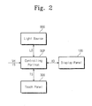
- FIG. 2 is a block diagram of the display device of the embodiment of the present invention shown in FIG. 1 ;
- FIG. 3 is a perspective view illustrating the outward appearance of a window substrate displayed when operating the display device of the embodiment of the present invention shown in FIG. 1 in a first mode;
- FIG. 4 is a cross sectional view taken along a line I-I' of FIG. 3 ;
- FIG. 5 is a perspective view illustrating the outward appearance of a window substrate displaying an icon when operating the display device of the embodiment of the present invention shown in FIG. 1 in a second mode;
- FIG. 6 is a cross sectional view taken along a line II-II' of FIG. 5 ;
- FIG. 7 is an enlarged cross sectional view of a portion AA of FIG. 6 ;
- FIG. 8 is a cross sectional view illustrating a portion of a display device according to other example embodiments of the present invention.
- FIG. 9 is a cross sectional view illustrating a portion of a display device according to still other example embodiments of the present invention.
- FIG. 10 is a cross sectional view illustrating a portion of a display device according to yet other example embodiments of the present invention.
- first, second, etc. may be used herein to describe various elements, components, regions, layers and/or sections, these elements, components, regions, layers and/or sections should not be limited by these terms. These terms are only used to distinguish one element, component, region, layer or section from another element, component, region, layer or section. Thus, a first element, component, region, layer or section discussed below could be termed a second element, component, region, layer or section without departing from the teachings of embodiments of the present invention.
- spatially relative terms such as “beneath,” “below,” “lower,” “above,” “upper” and the like, may be used herein for ease of description to describe one element or feature's relationship to another element(s) or feature(s) as illustrated in the figures. It will be understood that the spatially relative terms are intended to encompass different orientations of the device in use or operation in addition to the orientation depicted in the figures. For example, if the device in the figures is turned over, elements described as “below” or “beneath” other elements or features would then be oriented “above” the other elements or features. Thus, the exemplary term “below” can encompass both an orientation of above and below. The device may be otherwise oriented (rotated 90 degrees or at other orientations) and the spatially relative descriptors used herein interpreted accordingly.
- Example embodiments of the present invention are described herein with reference to cross-sectional illustrations that are schematic illustrations of idealized embodiments (and intermediate structures) of example embodiments of the present invention. As such, variations from the shapes of the illustrations as a result, for example, of manufacturing techniques and/or tolerances, are to be expected. Thus, embodiments of the present invention should not be construed as limited to the particular shapes of regions illustrated herein but are to include deviations in shapes that result, for example, from manufacturing. For example, an implanted region illustrated as a rectangle may have rounded or curved features and/or a gradient of implant concentration at its edges rather than a binary change from implanted to non-implanted region.
- a buried region formed by implantation may result in some implantation in the region between the buried region and the surface through which the implantation takes place.
- the regions illustrated in the figures are schematic in nature and their shapes are not intended to illustrate the actual shape of a region of a device and are not intended to limit the scope of embodiments of the present invention.
- FIG. 1 is an exploded perspective view of a display device according to one embodiment of the present invention
- FIG. 2 is a block diagram of the display device the embodiment of the present invention shown in FIG. 1 .
- a display device includes a display panel 100, a housing 200 containing the display panel 100, a touch panel 300 disposed on the display panel 100, and a window substrate 400 disposed on the touch panel 300.
- the display device is a component of a cellular phone, but the present invention is not limited thereto.
- the display device may be a component of one of various information service devices, such as a television set, a navigation system, a computer monitor, a game machine, and so forth.
- the display panel 100 is configured to display an image.
- the present invention is not limited to a specific type of the display panel.
- the display panel 100 may be one of various display panels, such as an organic light emitting display panel, a liquid crystal display panel, a plasma display panel, a electrophoretic display panel, an electrowetting display panel, and so forth.
- the housing 200 is configured to contain the display panel 100.
- the housing 200 includes one substrate, but the present invention is not limited thereto.
- the housing 200 may include two or more substrates, which are joined to each other.
- the housing 200 includes one substrate will be described.
- the housing 200 is configured to further include a printed circuit board (PCB) provided with a plurality of active devices and/or a plurality of passive devices in addition to the display panel 100. Furthermore, the housing 200 contains an electric power supplying portion, such as a battery.
- PCB printed circuit board
- the touch panel 300 is provided to obtain information on coordinates of a touch point, which will be input by a user.
- the touch panel 300 may be, for example, a resistive touch panel or a capacitive touch panel.
- the resistive touch panel is an analog resistive touch panel including two resistive layers spaced apart from each other or a digital resistive touch panel including first resistive patterns and second resistive patterns spaced apart from the first resistive patterns.
- the resistive touch panel is configured to detect a variation of output voltage occurring when the two resistive layers or the first and second resistive patterns are in contact with each other by an external force, and the detected variation of output voltage is used to calculate coordinate information of a touch point at which the external force is exerted.
- the capacitive touch panel includes first sensing patterns and second sensing patterns electrically isolated from the first sensing patterns.
- the first sensing patterns are disposed to cross the second sensing patterns.
- the capacitive touch panel is configured to detect a variation of electrical capacitance between the first and second sensing patterns occurring when the capacitive touch panel is touched by an input device (e.g., a stylus or a finger), and the detected variation of electrical capacitance is used to calculate coordinate information of a touch point.
- an input device e.g., a stylus or a finger
- the window substrate 400 is disposed on the touch panel 300 and is joined to the housing 200 to form an exterior of the display device along with the housing 200.
- the touch panel 300 is joined to the window substrate 400.
- the window substrate 400 includes a display region AR displaying an image generated by the display panel 100 and a non-display region NAR disposed adjacent to at least one portion of the display region AR.
- the non-display region NAR is configured to prevent an image from being outwardly displayed.
- the non-display region NAR includes an input icon region NAR-I.
- an opening 420-OP of a light shielding layer 420 is formed in the input icon region NAR-I.
- the display device further includes a light source 500 contained in the housing 200.
- the light source 500 is configured to generate a light that will be supplied into (or through) the input icon region NAR-I. Furthermore, the light source 500 is configured to supply the light into (or through) the input icon region NAR-I only when the display device is operated in a specific mode.
- a controlling portion DCP is realized using the active devices mounted on the PCB previously described with reference to FIG. 1 .
- One of the active devices is a microprocessor configured to supply an image signal to the display panel 100.
- another of the active devices is a microprocessor configured to calculate coordinate information of a touch point of the touch panel 300, at which an external input is exerted (or supplied, e.g., the point of the touch panel 300 or the window substrate 400 that a stylus or finger touches).
- the controlling portion DCP When an operation starting signal IS (e.g., pushing a power button is transmitted to the controlling portion DCP, the controlling portion DCP operates the display panel 100 and the touch panel 300 using a power voltage Vd supplied from an external or internal power supplying device.
- the display panel 100 displays an image based on an image signal ID, which may be stored in a memory device or which may be transmitted (e.g., received) from an external device.
- the controlling portion DCP is configured to supply a light source operating signal LS to the light source 500.
- the light source operating signal LS is generated on the basis of a coordinate information signal TS supplied from the touch panel 300.
- first mode will be used to refer to an operation mode of the display device in which the controlling portion DCP does not output the light source operating signal LS to the light source 500
- second mode will be used to refer to an operation mode of the display device, in which the controlling portion DCP outputs the light source operating signal LS to light source 500.
- FIG. 3 is a perspective view illustrating the outward appearance of a window substrate when operating the display device shown in FIG. 1 in a first mode
- FIG. 4 is a cross sectional view taken along a line I-I' of FIG. 3
- FIG. 5 is a perspective view illustrating the outward appearance of a window substrate displayed when operating the display device shown in FIG. 1 in a second mode
- FIG. 6 is a cross sectional view taken along a line II-II' of FIG. 5
- FIG. 7 is an enlarged cross sectional view of a portion AA of FIG. 6 .
- window substrate 400 will be described in more detail with reference to FIGS. 3, 4 , 5, 6 , and 7 .
- the window substrate 400 includes a base substrate 410, a light shielding layer 420 provided with at least one opening 420-OP, and a filter layer 430.
- the base substrate 410 is a transparent, plate-shaped substrate.
- the base substrate 410 includes a display region AR, which the image can be transmitted through, and a non-display region NAR disposed adjacent to at least one portion of the display region AR.
- the display region AR is enclosed (or surrounded or bordered) with the non-display region NAR, but embodiments of the present invention may not be limited thereto.
- the hon-display region NAR may include two separate regions spaced apart from each other by the display region AR.
- the base substrate 410 may include a glass or a plastic.
- the base substrate 410 may be formed of a tempered glass or a transparent reinforced plastic (e.g., polycarbonate).
- the light shielding layer 420 is disposed on one surface of the base substrate 410 to cover at least one portion of the non-display region NAR.
- the light shielding layer 420 is formed of a material capable of absorbing or reflecting a light incident from the other (or opposite) surface of the base substrate 410.
- the light shielding layer 420 includes at least one opening 420-OP. In some embodiments, as shown, for example, in FIGS. 3 and 5 , the light shielding layer 420 includes two openings 420-OP and covers the entire region of the non-display region NAR, but embodiments of the present invention are not limited thereto.
- a planar shape of the opening 420-OP may be variously modified.
- the opening 420-OP may be formed to have a shape (e.g., a graphical shape) indicating a specific function (e.g., a telephone-receiver-shaped opening or an arrow-shaped opening) or a letter shape.
- the opening 420-OP may be perceived by a user as an input icon.
- the filter layer 430 is disposed on one surface of the base substrate 410 provided with the light shielding layer 420 and is aligned with the opening 420-OP of the light shielding layer 420.
- the filter layer 430 is configured to partially transmit light (hereinafter referred to as "internal light") emitted from the light source 500 toward the opening 420-OP (e.g., light passing through the opening).
- the opening 420-OP is filled with the filter layer 430.
- the formation of the filter layer 430 may include forming a filtering material on a portion of the light shielding layer 420 (e.g., in the opening 420-OP) and then drying the filtering material.
- the filter layer 430 extends from the opening 420-OP and covers the light shielding layer 420 around the opening 420-OP.
- the filter layer 430 includes a plurality of first particles 430B and a plurality of second particles 430P.
- the first particles 430B are formed of a material capable of blocking the transmission of light
- the second particles 430P are formed of a material capable of transmitting light.
- the filter layer 430 may further include an additive, such as a surfactant, an adhesive, and so forth.
- the filter layer 430 reflects most of the light (hereinafter referred to as "external light") incident from the exterior into the opening 420-OP (e.g., light passing through the opening). Even if a part of the external light passes through the filter layer 430, an intensity of the part of the external light passing through the filter layer 430 is very low compared with an intensity of the internal light, and therefore, it is difficult for a user to perceive the opening 420-OP.
- the first particle 430B have substantially the same color as the light shielding layer 420. That is, the first particle 430B is formed of a material displaying (or that reflects) substantially the same color as that realized (e.g., displayed or reflected) by the light shielding layer 420. In this case, it is hard for the user to perceive the opening 420-OP.
- embodiments of the present invention are not limited to the case that the first particle 430B has the same color as the light shielding layer 420. In other words, the first particle 430B may have a different color from the light shielding layer 420.
- the light shielding layer 420 may be formed of a material having (e.g., displaying or reflecting) one color of black, white, red, green, or brown, while the first particle 430B may be formed of a material having the same color as the light shielding layer 420 but having a brightness or a chroma different from the light shielding layer 420.
- the above described effect can be obtained from, for example, the window substrate 400 including a black light shielding layer 420 and a brown or navy first particles 430B.
- the opening 420-OP When the internal light is incident into the opening 420-OP as shown in FIG. 6 , the opening 420-OP is perceived by a user as an input icon, as shown in FIG. 5 .
- the first particles 430B block transmission of the internal light, but the substantially transparent second particles 430P allow transmission of the internal light.
- the intensity of the internal light which is emitted from the base substrate 410 through the filter layer 430 depends on a ratio of the first particles 430B to the second particles 430P.
- the opening 420-OP may be perceived as an input icon by the external user, even when the internal light is not generated.
- a weight ratio of the first particles 430B to the second particles 430P are in a range of 8:1 to 12:1. In this case, about 0.1 % to about 0.27% of the internal light is transmitted through the filter layer 430.
- first particles 430B are black.
- a ratio of the first particles 430B to the second particles 430P may vary depending on color of the first particles 430B.
- the first particles 430B are white.
- the weight ratio of the first particles 430B to the second particles 430P is in a range of 1.5:1 to 2.5:1, and about 0.3% to about 1.2% of the internal light is transmitted through the filter layer 430.
- FIG. 8 is a cross sectional view illustrating a portion of a display device according to other example embodiments of the present invention.
- a display device according to embodiments of the present invention will be described in more detail with reference to FIG. 8 .
- components previously described with reference to FIGS. 1 through 7 may be identified by like reference numbers without repeating descriptions thereof.
- the light source 500 of the display device includes a light emitting device 510 and a light guide plate 520.
- the light guide plate 520 is disposed below the light shielding layer 420 to face the opening 420-OP or the input icon region NAR-I, and the light emitting device 510 is disposed at one side of the light guide plate 520.
- the light emitting device 510 is a light emitting diode.
- the light emitting diode generates light (hereinafter referred to as "originating light") in response to an operating voltage supplied from the exterior (e.g., a power source).
- the light emitting diode may be a semiconductor device having, for example, low power consumption, an increased luminous intensity, and a long lifetime.
- the light emitting diode is mounted on a PCB in a form of package and then installed in the housing 200.
- the light guide plate 520 is configured to guide the originating light to the opening 420-OP, for example, with a spatially uniform (or substantially uniform) intensity.
- the light guide plate 520 is shaped like a tetragonal (e.g., rectangular or square) plate.
- the light guide plate 520 is formed of a transparent material having enhanced mechanical strength and enhanced heat resistance.
- the light guide plate 520 may be formed of polycarbonate or acrylic resin.
- the light guide plate 520 has a side surface 521 adjacent to the light emitting device 510, an emitting surface 522 facing the filter layer 430, and a reflective surface 523 facing and parallel to the emitting surface 522.
- the originating light is incident into the light guide plate 520 through the side surface 521 and then emitted to the exterior of the light guide plate 520 through the emitting surface 522 directly or after being reflected by the reflective surface 523.
- FIG. 9 is a sectional view illustrating a portion of a display device according to still other example embodiments of the present invention.
- a display device according to one embodiment of the present invention will be described in more detail with reference to FIG. 9 .
- components previously described with reference to FIGS. 1 through 7 may be identified by like reference numbers without repeating descriptions thereof.
- the window substrate 400 further includes a first color layer 440.
- the first color layer 440 is disposed on a surface of the base substrate 410 provided with the filter layer 430 and is aligned to face the filter layer 430. Due to the presence of the first color layer 440, the internal light incident toward the opening 420-OP has a first color. In other words, the first color layer 440 causes a light having a specific color to pass therethrough.
- the internal light has the red color after passing through the first color layer 440.
- the red light passes through the filter layer 430 and is perceived as a red image by a user.
- a color of a light generated from the light source 500 is different from a color of the first color layer 440.
- the light source 500 may generate blue light and the first color layer 440 may have a yellow color, and in this case, light emitted from the opening 420-OP has a substantially white color or a white-like color.
- FIG. 10 is a sectional view illustrating a portion of a display device according to yet other example embodiments of the present invention.
- a display device according to embodiments of the present invention will be described in more detail with reference to FIG. 10 .
- components previously described with reference to FIGS. 1 through 7 may be identified by like reference numbers without repeating descriptions thereof.
- the window substrate 400 further includes a second color layer 450 interposed between the base substrate 410 and the light shielding layer 420.
- the second color layer 450 has a chromatic color, such as white, red, green, and so forth.
- the second color layer 450 has a shape corresponding to that of the light shielding layer 420.
- the second color layer 450 is disposed on a surface of the base substrate 410 to have the substantially same shape as the non-display region NAR.
- the light shielding layer 420 is disposed on the second color layer 450 to have the substantially same shape as the second color layer 450.
- the second color layer 450 and the light shielding layer 420 are sequentially stacked on a surface of the base substrate 410.
- a color perceived by a viewer is determined by a color of the second color layer 450.
- the external light may be partially or fully blocked by the second color layer 450, and a portion of the external light passing through the second color layer 450 may be blocked by the light shielding layer 420.
- the first particles 430B in the filter layer 430 are formed of a material capable of displaying the substantially same color as that realized by the second color layer 450.
- the second color layer 450 has an opening, which is formed to face the opening 420-OP of the light shielding layer 420.
- the opening of the second color layer 450 is filled with the filter layer 430.
- a window substrate for a display device is configured to be able to display at least one input icon.
- the input icon is defined by the opening provided in the light shielding layer.
- the window substrate 400 includes a filter layer 430, which is disposed on the opening to allow partial transmission of an incident light.
- a display device includes the window substrate.
- the input icon is perceived by a viewer only when the device is operated in a specific mode.
Landscapes
- Engineering & Computer Science (AREA)
- Theoretical Computer Science (AREA)
- Physics & Mathematics (AREA)
- Computer Hardware Design (AREA)
- General Engineering & Computer Science (AREA)
- General Physics & Mathematics (AREA)
- Human Computer Interaction (AREA)
- Optics & Photonics (AREA)
- Devices For Indicating Variable Information By Combining Individual Elements (AREA)
- Liquid Crystal (AREA)
- Position Input By Displaying (AREA)
- Electroluminescent Light Sources (AREA)
Abstract
Description
- The present invention relates to a window substrate and a display device including the same.
- Ongoing research has been performed on various display devices, such as television sets, navigation systems, computer monitors, game machines, and so forth.
- The display devices are often configured to have a plurality of buttons for operating functions, for example, controlling a volume level or selecting a menu item. In conventional display devices, the display devices have been equipped with buttons in independent ways. Recently however, some display devices have been configured to include a touch panel which allows the buttons to be integrated onto one input plane.
- The display devices having embedded touch panels include a window substrate including at least one input icon associated with a particular function. The device can be operated for a user's intended purpose by selecting an input icon associated with a desired function.
- However in such display devices, the input icons are typically always perceivable by a user, regardless of an operation of the display device. For example, the input icons can be perceived by a user, even when the display device is in an off-state.
- The present invention provides a window substrate and a display device including the same. The present invention aims to provide a window substrate that is configured to display at least one input icon that can only be perceived by a viewer when the display is in a specific mode.
- According to the present invention, a window substrate for a display device includes a base substrate including a display region and a non-display region adjacent to at least one portion of the display region, a light shielding layer on the base substrate and facing at least one portion of the non-display region, the light shielding layer having at least one opening, and a filter layer on the base substrate and facing the opening, the filter layer being adapted to transmit a portion of a light passing through the opening.
- A display device according to the present invention includes a display panel configured to display an image, a housing configured to contain the display panel, a touch panel on the display panel, and a window substrate on the touch panel.
- The filter layer may include a plurality of first particles adapted to block the incident light and a plurality of second particles adapted to transmit the incident light.
- In some embodiments, the first particles and the light shielding layer have substantially the same color as each other. The first particles may be black, and a weight ratio of the first particles to the second particles may be in a range from 8:1 to 12:1. The first particles may be white, and a weight ratio of the first particles to the second particles may be in a range from 1.5:1 to 2.5:1.
- The window substrate may further include a color layer interposed between the base substrate and the light shielding layer.
- The first particles and the color layer may have substantially the same color as each other.
- The window substrate may further include a color layer on the base substrate and adapted to filter a specific color of the incident light.
- The base substrate may include a tempered glass or a reinforced plastic. The light shielding layer may be directly on the base substrate and may have substantially the same planar shape as the non-display region.
- The display device may further include a light source portion in the housing and configured to generate the incident light. The light source portion may include a light emitting device adapted to generate an originating light and a light guide plate adapted to guide the originating light toward the window substrate, wherein the incident light includes a portion of the originating light emitted from the light guide plate.
- The accompanying drawings, together with the specification, illustrate embodiments of the present invention, and, together with the description, serve to explain the principles of the present invention.
FIGS. 1 through 10 represent non-limiting, example embodiments as described herein. -
FIG. 1 is an exploded perspective view of a display device according to one embodiment of the present invention; -
FIG. 2 is a block diagram of the display device of the embodiment of the present invention shown inFIG. 1 ; -
FIG. 3 is a perspective view illustrating the outward appearance of a window substrate displayed when operating the display device of the embodiment of the present invention shown inFIG. 1 in a first mode; -
FIG. 4 is a cross sectional view taken along a line I-I' ofFIG. 3 ; -
FIG. 5 is a perspective view illustrating the outward appearance of a window substrate displaying an icon when operating the display device of the embodiment of the present invention shown inFIG. 1 in a second mode; -
FIG. 6 is a cross sectional view taken along a line II-II' ofFIG. 5 ; -
FIG. 7 is an enlarged cross sectional view of a portion AA ofFIG. 6 ; -
FIG. 8 is a cross sectional view illustrating a portion of a display device according to other example embodiments of the present invention; -
FIG. 9 is a cross sectional view illustrating a portion of a display device according to still other example embodiments of the present invention; and -
FIG. 10 is a cross sectional view illustrating a portion of a display device according to yet other example embodiments of the present invention. - It should be noted that these figures are intended to illustrate the general characteristics of methods, structure and/or materials utilized in certain example embodiments and to supplement the written description provided below. These drawings are not, however, to scale and may not precisely reflect the precise structural or performance characteristics of any given embodiment, and should not be interpreted as defining or limiting the range of values or properties encompassed by embodiments of the present invention. For example, the relative thicknesses and positioning of molecules, layers, regions and/or structural elements may be reduced or exaggerated for clarity. The use of similar or identical reference numbers in the various drawings is intended to indicate the presence of a similar or identical element or feature.
- Embodiments of the present invention will now be described more fully with reference to the accompanying drawings, in which example embodiments of the present invention are shown. Embodiments of the present invention may, however, be embodied in many different forms and should not be construed as being limited to the embodiments set forth herein; rather, these embodiments are provided so that this disclosure will be thorough and complete, and will fully convey the concept of embodiments of the present invention to those of ordinary skill in the art. In the drawings, the thicknesses of layers and regions are exaggerated for clarity. Like reference numerals in the drawings denote like elements, and thus their description will be omitted.
- It will be understood that when an element is referred to as being "connected" or "coupled" to another element, it can be directly connected or coupled to the other element or intervening elements may be present. When an element is referred to as being "directly connected" or "directly coupled" to another element, there may be no intervening elements present. Like numbers indicate like elements throughout. As used herein the term "and/or" includes any and all combinations of one or more of the associated listed items. Other words used to describe the relationship between elements or layers should be interpreted in a like fashion (e.g., "between" versus "directly between," "adjacent" versus "directly adjacent," "on" versus "directly on").
- It will be understood that, although the terms "first", "second", etc. may be used herein to describe various elements, components, regions, layers and/or sections, these elements, components, regions, layers and/or sections should not be limited by these terms. These terms are only used to distinguish one element, component, region, layer or section from another element, component, region, layer or section. Thus, a first element, component, region, layer or section discussed below could be termed a second element, component, region, layer or section without departing from the teachings of embodiments of the present invention.
- Spatially relative terms, such as "beneath," "below," "lower," "above," "upper" and the like, may be used herein for ease of description to describe one element or feature's relationship to another element(s) or feature(s) as illustrated in the figures. It will be understood that the spatially relative terms are intended to encompass different orientations of the device in use or operation in addition to the orientation depicted in the figures. For example, if the device in the figures is turned over, elements described as "below" or "beneath" other elements or features would then be oriented "above" the other elements or features. Thus, the exemplary term "below" can encompass both an orientation of above and below. The device may be otherwise oriented (rotated 90 degrees or at other orientations) and the spatially relative descriptors used herein interpreted accordingly.
- The terminology used herein is for the purpose of describing particular embodiments only and is not intended to be limiting of embodiments of the present invention. As used herein, the singular forms "a," "an" and "the" are intended to include the plural forms as well, unless the context clearly indicates otherwise. It will be further understood that the terms "comprises", "comprising", "includes" and/or "including," if used herein, specify the presence of stated features, integers, steps, operations, elements and/or components, but do not preclude the presence or addition of one or more other features, integers, steps, operations, elements, components and/or groups thereof.
- Example embodiments of the present invention are described herein with reference to cross-sectional illustrations that are schematic illustrations of idealized embodiments (and intermediate structures) of example embodiments of the present invention. As such, variations from the shapes of the illustrations as a result, for example, of manufacturing techniques and/or tolerances, are to be expected. Thus, embodiments of the present invention should not be construed as limited to the particular shapes of regions illustrated herein but are to include deviations in shapes that result, for example, from manufacturing. For example, an implanted region illustrated as a rectangle may have rounded or curved features and/or a gradient of implant concentration at its edges rather than a binary change from implanted to non-implanted region. Likewise, a buried region formed by implantation may result in some implantation in the region between the buried region and the surface through which the implantation takes place. Thus, the regions illustrated in the figures are schematic in nature and their shapes are not intended to illustrate the actual shape of a region of a device and are not intended to limit the scope of embodiments of the present invention.
- Unless otherwise defined, all terms (including technical and scientific terms) used herein have the same meaning as commonly understood by one of ordinary skill in the art to which embodiments of the present invention belong. It will be further understood that terms, such as those defined in commonly-used dictionaries, should be interpreted as having a meaning that is consistent with their meaning in the context of the relevant art and will not be interpreted in an idealized or overly formal sense unless expressly so defined herein.
-
FIG. 1 is an exploded perspective view of a display device according to one embodiment of the present invention, andFIG. 2 is a block diagram of the display device the embodiment of the present invention shown inFIG. 1 . - A display device according to example embodiments of the present invention includes a
display panel 100, ahousing 200 containing thedisplay panel 100, atouch panel 300 disposed on thedisplay panel 100, and awindow substrate 400 disposed on thetouch panel 300. - In the embodiments, shown in
FIGS. 1 and2 , the display device is a component of a cellular phone, but the present invention is not limited thereto. For example, the display device may be a component of one of various information service devices, such as a television set, a navigation system, a computer monitor, a game machine, and so forth. - The
display panel 100 is configured to display an image. The present invention is not limited to a specific type of the display panel. For example, thedisplay panel 100 may be one of various display panels, such as an organic light emitting display panel, a liquid crystal display panel, a plasma display panel, a electrophoretic display panel, an electrowetting display panel, and so forth. - The
housing 200 is configured to contain thedisplay panel 100. In some embodiments, as shown, for example, inFIG. 1 , thehousing 200 includes one substrate, but the present invention is not limited thereto. For example, thehousing 200 may include two or more substrates, which are joined to each other. Hereinafter, for the sake of convenience, embodiments of the present in which thehousing 200 includes one substrate will be described. - The
housing 200 is configured to further include a printed circuit board (PCB) provided with a plurality of active devices and/or a plurality of passive devices in addition to thedisplay panel 100. Furthermore, thehousing 200 contains an electric power supplying portion, such as a battery. - The
touch panel 300 is provided to obtain information on coordinates of a touch point, which will be input by a user. Thetouch panel 300 may be, for example, a resistive touch panel or a capacitive touch panel. - The resistive touch panel is an analog resistive touch panel including two resistive layers spaced apart from each other or a digital resistive touch panel including first resistive patterns and second resistive patterns spaced apart from the first resistive patterns. The resistive touch panel is configured to detect a variation of output voltage occurring when the two resistive layers or the first and second resistive patterns are in contact with each other by an external force, and the detected variation of output voltage is used to calculate coordinate information of a touch point at which the external force is exerted.
- The capacitive touch panel includes first sensing patterns and second sensing patterns electrically isolated from the first sensing patterns. Here, the first sensing patterns are disposed to cross the second sensing patterns. The capacitive touch panel is configured to detect a variation of electrical capacitance between the first and second sensing patterns occurring when the capacitive touch panel is touched by an input device (e.g., a stylus or a finger), and the detected variation of electrical capacitance is used to calculate coordinate information of a touch point.
- The
window substrate 400 is disposed on thetouch panel 300 and is joined to thehousing 200 to form an exterior of the display device along with thehousing 200. In some embodiments, thetouch panel 300 is joined to thewindow substrate 400. - In a plan view, the
window substrate 400 includes a display region AR displaying an image generated by thedisplay panel 100 and a non-display region NAR disposed adjacent to at least one portion of the display region AR. - The non-display region NAR is configured to prevent an image from being outwardly displayed. In addition, in the embodiment shown in
FIG. 1 , the non-display region NAR includes an input icon region NAR-I. As will be described below, an opening 420-OP of alight shielding layer 420 is formed in the input icon region NAR-I. - The display device further includes a
light source 500 contained in thehousing 200. Thelight source 500 is configured to generate a light that will be supplied into (or through) the input icon region NAR-I. Furthermore, thelight source 500 is configured to supply the light into (or through) the input icon region NAR-I only when the display device is operated in a specific mode. - Hereinafter, an operating method of a display device according to example embodiments of the present invention will be described with reference to
FIG. 2 . A controlling portion DCP, as shown inFIG. 2 , is realized using the active devices mounted on the PCB previously described with reference toFIG. 1 . One of the active devices is a microprocessor configured to supply an image signal to thedisplay panel 100. In addition, another of the active devices is a microprocessor configured to calculate coordinate information of a touch point of thetouch panel 300, at which an external input is exerted (or supplied, e.g., the point of thetouch panel 300 or thewindow substrate 400 that a stylus or finger touches). - When an operation starting signal IS (e.g., pushing a power button is transmitted to the controlling portion DCP, the controlling portion DCP operates the
display panel 100 and thetouch panel 300 using a power voltage Vd supplied from an external or internal power supplying device. Thedisplay panel 100 displays an image based on an image signal ID, which may be stored in a memory device or which may be transmitted (e.g., received) from an external device. - The controlling portion DCP is configured to supply a light source operating signal LS to the
light source 500. The light source operating signal LS is generated on the basis of a coordinate information signal TS supplied from thetouch panel 300. - Hereinafter, a term "first mode" will be used to refer to an operation mode of the display device in which the controlling portion DCP does not output the light source operating signal LS to the
light source 500, and a term "second mode" will be used to refer to an operation mode of the display device, in which the controlling portion DCP outputs the light source operating signal LS tolight source 500. -
FIG. 3 is a perspective view illustrating the outward appearance of a window substrate when operating the display device shown inFIG. 1 in a first mode, andFIG. 4 is a cross sectional view taken along a line I-I' ofFIG. 3 .FIG. 5 is a perspective view illustrating the outward appearance of a window substrate displayed when operating the display device shown inFIG. 1 in a second mode, andFIG. 6 is a cross sectional view taken along a line II-II' ofFIG. 5 .FIG. 7 is an enlarged cross sectional view of a portion AA ofFIG. 6 . - Hereinafter, the
window substrate 400 will be described in more detail with reference toFIGS. 3, 4 ,5, 6 , and7 . - According to one embodiment of the present invention, the
window substrate 400 includes abase substrate 410, alight shielding layer 420 provided with at least one opening 420-OP, and afilter layer 430. - The
base substrate 410 is a transparent, plate-shaped substrate. In a plan view, thebase substrate 410 includes a display region AR, which the image can be transmitted through, and a non-display region NAR disposed adjacent to at least one portion of the display region AR. - As shown in
FIGS. 3 and5 , the display region AR is enclosed (or surrounded or bordered) with the non-display region NAR, but embodiments of the present invention may not be limited thereto. For example, in a plan view, the hon-display region NAR may include two separate regions spaced apart from each other by the display region AR. - The
base substrate 410 may include a glass or a plastic. For example, thebase substrate 410 may be formed of a tempered glass or a transparent reinforced plastic (e.g., polycarbonate). - The
light shielding layer 420 is disposed on one surface of thebase substrate 410 to cover at least one portion of the non-display region NAR. Thelight shielding layer 420 is formed of a material capable of absorbing or reflecting a light incident from the other (or opposite) surface of thebase substrate 410. - The
light shielding layer 420 includes at least one opening 420-OP. In some embodiments, as shown, for example, inFIGS. 3 and5 , thelight shielding layer 420 includes two openings 420-OP and covers the entire region of the non-display region NAR, but embodiments of the present invention are not limited thereto. - According to example embodiments of the present invention, a planar shape of the opening 420-OP may be variously modified. For example, in a plan view, the opening 420-OP may be formed to have a shape (e.g., a graphical shape) indicating a specific function (e.g., a telephone-receiver-shaped opening or an arrow-shaped opening) or a letter shape. In some embodiments, the opening 420-OP may be perceived by a user as an input icon.
- According to one embodiment of the present invention, the
filter layer 430 is disposed on one surface of thebase substrate 410 provided with thelight shielding layer 420 and is aligned with the opening 420-OP of thelight shielding layer 420. Thefilter layer 430 is configured to partially transmit light (hereinafter referred to as "internal light") emitted from thelight source 500 toward the opening 420-OP (e.g., light passing through the opening). - In some embodiments of the present invention, the opening 420-OP is filled with the
filter layer 430. The formation of thefilter layer 430 may include forming a filtering material on a portion of the light shielding layer 420 (e.g., in the opening 420-OP) and then drying the filtering material. In some embodiments, thefilter layer 430 extends from the opening 420-OP and covers thelight shielding layer 420 around the opening 420-OP. - According to one embodiment of the present invention, as shown in
FIG. 7 , thefilter layer 430 includes a plurality offirst particles 430B and a plurality ofsecond particles 430P. Thefirst particles 430B are formed of a material capable of blocking the transmission of light, and thesecond particles 430P are formed of a material capable of transmitting light. In addition, thefilter layer 430 may further include an additive, such as a surfactant, an adhesive, and so forth. - If the internal light is not incident on the opening 420-OP, it may be difficult for a user to perceive the opening 420-OP, as shown in
FIG. 3 . Thefilter layer 430 reflects most of the light (hereinafter referred to as "external light") incident from the exterior into the opening 420-OP (e.g., light passing through the opening). Even if a part of the external light passes through thefilter layer 430, an intensity of the part of the external light passing through thefilter layer 430 is very low compared with an intensity of the internal light, and therefore, it is difficult for a user to perceive the opening 420-OP. - In some embodiments, the
first particle 430B have substantially the same color as thelight shielding layer 420. That is, thefirst particle 430B is formed of a material displaying (or that reflects) substantially the same color as that realized (e.g., displayed or reflected) by thelight shielding layer 420. In this case, it is hard for the user to perceive the opening 420-OP. However, embodiments of the present invention are not limited to the case that thefirst particle 430B has the same color as thelight shielding layer 420. In other words, thefirst particle 430B may have a different color from thelight shielding layer 420. - For instance, the
light shielding layer 420 may be formed of a material having (e.g., displaying or reflecting) one color of black, white, red, green, or brown, while thefirst particle 430B may be formed of a material having the same color as thelight shielding layer 420 but having a brightness or a chroma different from thelight shielding layer 420. In other embodiments, the above described effect can be obtained from, for example, thewindow substrate 400 including a blacklight shielding layer 420 and a brown or navyfirst particles 430B. - When the internal light is incident into the opening 420-OP as shown in
FIG. 6 , the opening 420-OP is perceived by a user as an input icon, as shown inFIG. 5 . - As shown in
FIG. 7 , thefirst particles 430B block transmission of the internal light, but the substantially transparentsecond particles 430P allow transmission of the internal light. - When the
light source 500 generates a light with a substantially uniform intensity, the intensity of the internal light which is emitted from thebase substrate 410 through thefilter layer 430, depends on a ratio of thefirst particles 430B to thesecond particles 430P. - For instance, in the case in which the number of
second particles 430P far outnumbers the number offirst particles 430B, transmission of the external light is increased. As a result, the opening 420-OP may be perceived as an input icon by the external user, even when the internal light is not generated. - For example, if the
first particles 430B are black, a weight ratio of thefirst particles 430B to thesecond particles 430P are in a range of 8:1 to 12:1. In this case, about 0.1 % to about 0.27% of the internal light is transmitted through thefilter layer 430. - However, the above mentioned range or ratio may be valid in the case that the
first particles 430B are black. In other embodiments of the present invention, a ratio of thefirst particles 430B to thesecond particles 430P may vary depending on color of thefirst particles 430B. - In other embodiments, the
first particles 430B are white. In this case, the weight ratio of thefirst particles 430B to thesecond particles 430P is in a range of 1.5:1 to 2.5:1, and about 0.3% to about 1.2% of the internal light is transmitted through thefilter layer 430. -
FIG. 8 is a cross sectional view illustrating a portion of a display device according to other example embodiments of the present invention. Hereinafter, a display device according to embodiments of the present invention will be described in more detail with reference toFIG. 8 . For the sake of convenience, components previously described with reference toFIGS. 1 through 7 may be identified by like reference numbers without repeating descriptions thereof. - According to one embodiment of the present invention, the
light source 500 of the display device includes alight emitting device 510 and alight guide plate 520. Thelight guide plate 520 is disposed below thelight shielding layer 420 to face the opening 420-OP or the input icon region NAR-I, and thelight emitting device 510 is disposed at one side of thelight guide plate 520. - In some embodiments of the present invention, the
light emitting device 510 is a light emitting diode. The light emitting diode generates light (hereinafter referred to as "originating light") in response to an operating voltage supplied from the exterior (e.g., a power source). The light emitting diode may be a semiconductor device having, for example, low power consumption, an increased luminous intensity, and a long lifetime. The light emitting diode is mounted on a PCB in a form of package and then installed in thehousing 200. - The
light guide plate 520 is configured to guide the originating light to the opening 420-OP, for example, with a spatially uniform (or substantially uniform) intensity. - The
light guide plate 520 is shaped like a tetragonal (e.g., rectangular or square) plate. Thelight guide plate 520 is formed of a transparent material having enhanced mechanical strength and enhanced heat resistance. For example, thelight guide plate 520 may be formed of polycarbonate or acrylic resin. - The
light guide plate 520 has aside surface 521 adjacent to thelight emitting device 510, an emittingsurface 522 facing thefilter layer 430, and areflective surface 523 facing and parallel to the emittingsurface 522. - The originating light is incident into the
light guide plate 520 through theside surface 521 and then emitted to the exterior of thelight guide plate 520 through the emittingsurface 522 directly or after being reflected by thereflective surface 523. -
FIG. 9 is a sectional view illustrating a portion of a display device according to still other example embodiments of the present invention. Hereinafter, a display device according to one embodiment of the present invention will be described in more detail with reference toFIG. 9 . For the sake of convenience, components previously described with reference toFIGS. 1 through 7 may be identified by like reference numbers without repeating descriptions thereof. - According to the present embodiments, the
window substrate 400 further includes afirst color layer 440. - The
first color layer 440 is disposed on a surface of thebase substrate 410 provided with thefilter layer 430 and is aligned to face thefilter layer 430. Due to the presence of thefirst color layer 440, the internal light incident toward the opening 420-OP has a first color. In other words, thefirst color layer 440 causes a light having a specific color to pass therethrough. - For example, in the case in which the
first color layer 440 has a red color, the internal light has the red color after passing through thefirst color layer 440. The red light passes through thefilter layer 430 and is perceived as a red image by a user. - In other embodiments of the present invention, a color of a light generated from the
light source 500 is different from a color of thefirst color layer 440. For example, thelight source 500 may generate blue light and thefirst color layer 440 may have a yellow color, and in this case, light emitted from the opening 420-OP has a substantially white color or a white-like color. -
FIG. 10 is a sectional view illustrating a portion of a display device according to yet other example embodiments of the present invention. Hereinafter, a display device according to embodiments of the present invention will be described in more detail with reference toFIG. 10 . For the sake of convenience, components previously described with reference toFIGS. 1 through 7 may be identified by like reference numbers without repeating descriptions thereof. - According to embodiments of the present invention, the
window substrate 400 further includes asecond color layer 450 interposed between thebase substrate 410 and thelight shielding layer 420. Thesecond color layer 450 has a chromatic color, such as white, red, green, and so forth. - In a plan view, the
second color layer 450 has a shape corresponding to that of thelight shielding layer 420. In more detail, thesecond color layer 450 is disposed on a surface of thebase substrate 410 to have the substantially same shape as the non-display region NAR. Thelight shielding layer 420 is disposed on thesecond color layer 450 to have the substantially same shape as thesecond color layer 450. In other words, as shown inFIG. 10 , thesecond color layer 450 and thelight shielding layer 420 are sequentially stacked on a surface of thebase substrate 410. - According to some aspects of embodiments of the present invention, a color perceived by a viewer is determined by a color of the
second color layer 450. Furthermore, the external light may be partially or fully blocked by thesecond color layer 450, and a portion of the external light passing through thesecond color layer 450 may be blocked by thelight shielding layer 420. - In some embodiments of the present invention, the
first particles 430B in thefilter layer 430 are formed of a material capable of displaying the substantially same color as that realized by thesecond color layer 450. - In some embodiments of the present invention, the
second color layer 450 has an opening, which is formed to face the opening 420-OP of thelight shielding layer 420. Here, the opening of thesecond color layer 450 is filled with thefilter layer 430. - According to embodiments of the present invention, a window substrate for a display device is configured to be able to display at least one input icon. The input icon is defined by the opening provided in the light shielding layer. The
window substrate 400 includes afilter layer 430, which is disposed on the opening to allow partial transmission of an incident light. - According to some aspects of the present invention, a display device includes the window substrate. Here, the input icon is perceived by a viewer only when the device is operated in a specific mode.
- While embodiments of the present invention have been particularly shown and described, it will be understood by one of ordinary skill in the art that variations in form and detail may be made therein without departing from the scope of the attached claims.
Claims (16)
- A window substrate for a display device, comprising:a base substrate (410) comprising a display region and a non-display region adjacent to at least one portion of the display region;a light shielding layer (420) on the base substrate and facing at least one portion of the non-display region, the light shielding layer having at least one opening; anda filter layer (430) on the base substrate and facing the opening, the filter layer being adapted to transmit a portion of a light passing through the opening.
- The window substrate of claim 1, wherein the filter layer comprises:a plurality of first particles (430B) adapted to block the incident light; anda plurality of second particles (430P) adapted to transmit the incident light.
- The window substrate of claim 2, wherein the first particles and the light shielding layer have substantially the same color as each other.
- The window substrate of claim 2 or 3, wherein the first particles have a black color, and a weight ratio of the first particles to the second particles is in a range from 8:1 to 12:1.
- The window substrate of claim 2 or 3, wherein the first particles have a white color, and a weight ratio of the first particles to the second particles is in a range from 1.5:1 to 2.5:1.
- The window substrate of claim 2, further comprising a color layer interposed between the base substrate and the light shielding layer.
- The window substrate of claim 6, wherein the first particles and the color layer have substantially the same color as each other.
- The window substrate of any one of the preceding claim 1, wherein the filter layer is filled with the opening.
- The window substrate of claim 8, wherein the filter layer and the opening have a substantially identical shape, and the filter layer and the light shielding layer are disposed on the same layer.
- The window substrate of claim 8, wherein the filter layer comprises:a first portion having the same shape as the opening and filling the opening; anda second portion being connected to the first portion and overlapping the light shielding layer.
- The window substrate of any one of the preceding claims, further comprising a color layer on the base substrate, the color layer facing the filter layer and adapted to filter a color of the incident light.
- The window substrate of any one of the preceding claims, wherein the base substrate comprises a tempered glass or a reinforced plastic.
- The window substrate of any one of the preceding claims, wherein the light shielding layer is directly on the base substrate and has substantially the same planar shape as the non-display region.
- A display device comprising:a display panel configured to display an image;a housing configured to contain the display panel;a touch panel on the display panel; anda window substrate according to any one of the preceding claims on the touch panel.
- The display device of claim 14, further comprising a light source portion in the housing and configured to generate the incident light.
- The display device of claim 15, wherein the light source portion comprises:a light emitting device adapted to generate an originating light; anda light guide plate adapted to guide the originating light toward the window substrate, wherein the incident light comprises a portion of the originating light emitted from the light guide plate.
Applications Claiming Priority (1)
| Application Number | Priority Date | Filing Date | Title |
|---|---|---|---|
| KR1020110090912A KR101451925B1 (en) | 2011-09-07 | 2011-09-07 | Window substrate for display device and display device having the same |
Publications (2)
| Publication Number | Publication Date |
|---|---|
| EP2568363A2 true EP2568363A2 (en) | 2013-03-13 |
| EP2568363A3 EP2568363A3 (en) | 2014-05-14 |
Family
ID=47076091
Family Applications (1)
| Application Number | Title | Priority Date | Filing Date |
|---|---|---|---|
| EP20120183478 Withdrawn EP2568363A3 (en) | 2011-09-07 | 2012-09-07 | Window substrate and display device having the same |
Country Status (6)
| Country | Link |
|---|---|
| US (1) | US9058154B2 (en) |
| EP (1) | EP2568363A3 (en) |
| JP (1) | JP5911282B2 (en) |
| KR (1) | KR101451925B1 (en) |
| CN (2) | CN102982735B (en) |
| TW (1) | TWI497125B (en) |
Cited By (2)
| Publication number | Priority date | Publication date | Assignee | Title |
|---|---|---|---|---|
| EP3197136A4 (en) * | 2015-07-24 | 2017-12-06 | Guangdong Oppo Mobile Telecommunications Corp., Ltd. | Display screen assembly, front cover of terminal, and terminal |
| EP3529648A4 (en) * | 2016-10-20 | 2020-06-10 | 3M Innovative Properties Company | Device optical window camouflage |
Families Citing this family (16)
| Publication number | Priority date | Publication date | Assignee | Title |
|---|---|---|---|---|
| KR101451925B1 (en) * | 2011-09-07 | 2014-10-23 | 삼성디스플레이 주식회사 | Window substrate for display device and display device having the same |
| KR101903348B1 (en) * | 2012-05-09 | 2018-10-05 | 삼성디스플레이 주식회사 | Display device and mathod for fabricating the same |
| US20150116235A1 (en) * | 2012-09-04 | 2015-04-30 | Mitsubishi Electric Corporation | Information apparatus |
| TWI472984B (en) * | 2012-12-27 | 2015-02-11 | Hannstouch Solution Inc | Touch panel and touch-controlled display device |
| KR20150112233A (en) * | 2014-03-27 | 2015-10-07 | 삼성전기주식회사 | Touch Sensor Module |
| CN104133592B (en) * | 2014-07-30 | 2017-05-24 | 业成光电(深圳)有限公司 | Curved surface touch device |
| JP6655344B2 (en) * | 2015-10-20 | 2020-02-26 | シャープ株式会社 | Operation unit and electronic device including the same |
| CN105677098B (en) * | 2016-01-05 | 2018-09-11 | 京东方科技集团股份有限公司 | A kind of touch screen and touch control device |
| KR102383915B1 (en) * | 2017-05-22 | 2022-04-08 | 삼성디스플레이 주식회사 | Display device |
| KR102436655B1 (en) * | 2017-09-22 | 2022-08-26 | 삼성디스플레이 주식회사 | Display device |
| CN110501838A (en) * | 2019-06-11 | 2019-11-26 | 惠科股份有限公司 | Display panel and display device |
| CN110456542B (en) * | 2019-06-11 | 2020-12-29 | 惠科股份有限公司 | Display panel and display device |
| CN110426874A (en) * | 2019-06-11 | 2019-11-08 | 惠科股份有限公司 | Display panel and display device |
| CN110441950B (en) * | 2019-06-11 | 2020-12-18 | 惠科股份有限公司 | Display panel and display device |
| CN110333622B (en) * | 2019-06-11 | 2021-01-08 | 惠科股份有限公司 | Display panel and display device |
| CN113346002B (en) * | 2020-06-05 | 2023-06-27 | 友达光电股份有限公司 | Display panel |
Citations (2)
| Publication number | Priority date | Publication date | Assignee | Title |
|---|---|---|---|---|
| US6747796B1 (en) * | 1999-05-11 | 2004-06-08 | Michael G. L. Dorling | High contrast screen material |
| US20080309589A1 (en) * | 2007-06-13 | 2008-12-18 | Morales Joseph M | Segmented Electroluminescent Device for Morphing User Interface |
Family Cites Families (26)
| Publication number | Priority date | Publication date | Assignee | Title |
|---|---|---|---|---|
| JPH07306648A (en) * | 1994-05-10 | 1995-11-21 | Yazaki Corp | Light leakage prevention structure for multi-lamp display |
| JP3899205B2 (en) * | 1999-05-31 | 2007-03-28 | アビリット株式会社 | Symbol variable display game machine |
| KR20060025616A (en) | 2004-09-17 | 2006-03-22 | 지콤코리아 주식회사 | Light emitting device on the side key of mobile phone |
| CN100490038C (en) | 2005-04-05 | 2009-05-20 | 华硕电脑股份有限公司 | Key and keyboard |
| EP1761002B1 (en) * | 2005-08-30 | 2013-12-18 | LG Electronics Inc. | Touch key assembly for a mobile terminal |
| US20080117635A1 (en) | 2006-11-17 | 2008-05-22 | Ko-Ju Chen | Multi-Layer Light Guiding Structure And Method For Using The Same |
| JP2008186373A (en) * | 2007-01-31 | 2008-08-14 | Seiko Instruments Inc | Portable electronic apparatus |
| US7582840B2 (en) | 2007-07-26 | 2009-09-01 | Sony Ericsson Mobile Communications Ab | User control interface |
| KR101410175B1 (en) | 2007-09-27 | 2014-06-19 | 삼성전자주식회사 | Portable communication device having touch key |
| KR20090087705A (en) * | 2008-02-13 | 2009-08-18 | 삼성코닝정밀유리 주식회사 | Optical filter for display device and display device having same |
| US20090284481A1 (en) * | 2008-05-17 | 2009-11-19 | Motorola, Inc. | Devices and Methods for a Backlight to Illuminate Both a Main Display and Morphable Keys or Indicators |
| CN101656530A (en) * | 2008-08-18 | 2010-02-24 | 海尔集团公司 | Luminous touch key and touch control module |
| JP5215108B2 (en) * | 2008-10-03 | 2013-06-19 | ソニーモバイルコミュニケーションズ株式会社 | Display device, display device forming method, key device, key device forming method, electronic device, and portable terminal device |
| KR200457113Y1 (en) * | 2008-10-23 | 2011-12-06 | (주) 태양기전 | Touch windows |
| KR101637565B1 (en) * | 2008-12-15 | 2016-07-07 | 엘지이노텍 주식회사 | Liquid crystal display device |
| JP4621814B2 (en) * | 2008-12-26 | 2011-01-26 | 日本写真印刷株式会社 | Protective panel with touch input function for electronic device display window and manufacturing method thereof |
| CN101782816A (en) * | 2009-01-21 | 2010-07-21 | 景发科技股份有限公司 | Touch panel with pressing touch and electronic device using it |
| CN201435069Y (en) * | 2009-04-01 | 2010-03-31 | 钰玺科技有限公司 | Touch-control keyboard input device with pattern switching |
| KR100940972B1 (en) * | 2009-04-22 | 2010-02-05 | 주식회사 엔에이치케이플러스 | Key-pad assembly for with light guide film |
| US8731618B2 (en) | 2009-04-23 | 2014-05-20 | Apple Inc. | Portable electronic device |
| CN201408519Y (en) * | 2009-05-19 | 2010-02-17 | 天津三星电子显示器有限公司 | Display with touch-sensitive luminous keys |
| KR101603235B1 (en) * | 2009-10-14 | 2016-03-14 | 엘지디스플레이 주식회사 | Liquid Crystal Display Device Attached Touch Panel |
| JP5522570B2 (en) * | 2010-01-29 | 2014-06-18 | ミネベア株式会社 | Keyboard device and electronic device using the same |
| KR101048974B1 (en) | 2010-04-01 | 2011-07-12 | 삼성모바일디스플레이주식회사 | Touch screen panel |
| KR101048931B1 (en) | 2010-04-01 | 2011-07-12 | 삼성모바일디스플레이주식회사 | Touch screen panel |
| KR101451925B1 (en) * | 2011-09-07 | 2014-10-23 | 삼성디스플레이 주식회사 | Window substrate for display device and display device having the same |
-
2011
- 2011-09-07 KR KR1020110090912A patent/KR101451925B1/en active Active
- 2011-12-08 JP JP2011268783A patent/JP5911282B2/en active Active
-
2012
- 2012-05-11 US US13/469,672 patent/US9058154B2/en active Active
- 2012-06-20 CN CN201210210666.0A patent/CN102982735B/en active Active
- 2012-06-20 CN CN2012202993744U patent/CN202948664U/en not_active Expired - Lifetime
- 2012-09-04 TW TW101132226A patent/TWI497125B/en active
- 2012-09-07 EP EP20120183478 patent/EP2568363A3/en not_active Withdrawn
Patent Citations (2)
| Publication number | Priority date | Publication date | Assignee | Title |
|---|---|---|---|---|
| US6747796B1 (en) * | 1999-05-11 | 2004-06-08 | Michael G. L. Dorling | High contrast screen material |
| US20080309589A1 (en) * | 2007-06-13 | 2008-12-18 | Morales Joseph M | Segmented Electroluminescent Device for Morphing User Interface |
Cited By (3)
| Publication number | Priority date | Publication date | Assignee | Title |
|---|---|---|---|---|
| EP3197136A4 (en) * | 2015-07-24 | 2017-12-06 | Guangdong Oppo Mobile Telecommunications Corp., Ltd. | Display screen assembly, front cover of terminal, and terminal |
| US10698509B2 (en) | 2015-07-24 | 2020-06-30 | Guangdong Oppo Mobile Telecommunications Corp., Ltd. | Display screen assembly, terminal front cover, and terminal |
| EP3529648A4 (en) * | 2016-10-20 | 2020-06-10 | 3M Innovative Properties Company | Device optical window camouflage |
Also Published As
| Publication number | Publication date |
|---|---|
| EP2568363A3 (en) | 2014-05-14 |
| TWI497125B (en) | 2015-08-21 |
| KR20130027371A (en) | 2013-03-15 |
| JP5911282B2 (en) | 2016-04-27 |
| CN102982735B (en) | 2016-05-11 |
| TW201314277A (en) | 2013-04-01 |
| US20130058128A1 (en) | 2013-03-07 |
| JP2013057920A (en) | 2013-03-28 |
| CN102982735A (en) | 2013-03-20 |
| US9058154B2 (en) | 2015-06-16 |
| KR101451925B1 (en) | 2014-10-23 |
| CN202948664U (en) | 2013-05-22 |
Similar Documents
| Publication | Publication Date | Title |
|---|---|---|
| US9058154B2 (en) | Window substrate and display device having the same | |
| KR102611245B1 (en) | Touch panel | |
| US9454237B2 (en) | Key assembly for electronic device | |
| KR20230113234A (en) | Touch panel | |
| US20100328223A1 (en) | Apparatus and associated methods | |
| CN102629165B (en) | Display assembly and terminal | |
| KR101285524B1 (en) | Input device | |
| CN101776816B (en) | Optical touch display panel | |
| CN203552209U (en) | Touch control panel and touch control display panel | |
| US9927567B2 (en) | Display with additional lighting effects | |
| KR20150042046A (en) | Touch sensor | |
| AU2011221666B2 (en) | Touch screen module structure | |
| US12225766B2 (en) | Display device and manufacturing method therefor | |
| US9542018B2 (en) | Touch panel and electronic apparatus | |
| TWI521395B (en) | Touch-controlled electronic apparatus and method for fabricating the touch-controlled electronic apparatus thereof | |
| JP2015055938A (en) | Display device with touch detection function, electronic device and cover material | |
| CN102446016B (en) | Electronic device and method of assembling the electronic device | |
| KR102661615B1 (en) | Bliquid crystal display device | |
| KR101735307B1 (en) | Mobile terminal and touch screen panel thereof | |
| CN206497391U (en) | Electronic equipment | |
| CN103837993A (en) | Touch Naked Eye Stereoscopic Display | |
| JP2012108835A (en) | Touch panel |
Legal Events
| Date | Code | Title | Description |
|---|---|---|---|
| PUAI | Public reference made under article 153(3) epc to a published international application that has entered the european phase |
Free format text: ORIGINAL CODE: 0009012 |
|
| 17P | Request for examination filed |
Effective date: 20120907 |
|
| AK | Designated contracting states |
Kind code of ref document: A2 Designated state(s): AL AT BE BG CH CY CZ DE DK EE ES FI FR GB GR HR HU IE IS IT LI LT LU LV MC MK MT NL NO PL PT RO RS SE SI SK SM TR |
|
| AX | Request for extension of the european patent |
Extension state: BA ME |
|
| PUAL | Search report despatched |
Free format text: ORIGINAL CODE: 0009013 |
|
| AK | Designated contracting states |
Kind code of ref document: A3 Designated state(s): AL AT BE BG CH CY CZ DE DK EE ES FI FR GB GR HR HU IE IS IT LI LT LU LV MC MK MT NL NO PL PT RO RS SE SI SK SM TR |
|
| AX | Request for extension of the european patent |
Extension state: BA ME |
|
| RIC1 | Information provided on ipc code assigned before grant |
Ipc: G06F 1/16 20060101ALN20140410BHEP Ipc: G06F 3/041 20060101AFI20140410BHEP |
|
| 17Q | First examination report despatched |
Effective date: 20150520 |
|
| RAP1 | Party data changed (applicant data changed or rights of an application transferred) |
Owner name: SAMSUNG DISPLAY CO., LTD. |
|
| APBK | Appeal reference recorded |
Free format text: ORIGINAL CODE: EPIDOSNREFNE |
|
| APBN | Date of receipt of notice of appeal recorded |
Free format text: ORIGINAL CODE: EPIDOSNNOA2E |
|
| APBR | Date of receipt of statement of grounds of appeal recorded |
Free format text: ORIGINAL CODE: EPIDOSNNOA3E |
|
| APAF | Appeal reference modified |
Free format text: ORIGINAL CODE: EPIDOSCREFNE |
|
| APBT | Appeal procedure closed |
Free format text: ORIGINAL CODE: EPIDOSNNOA9E |
|
| STAA | Information on the status of an ep patent application or granted ep patent |
Free format text: STATUS: THE APPLICATION IS DEEMED TO BE WITHDRAWN |
|
| 18D | Application deemed to be withdrawn |
Effective date: 20200401 |