EP2567436B1 - Power management circuit for a wireless communication device and process control system using same - Google Patents
Power management circuit for a wireless communication device and process control system using same Download PDFInfo
- Publication number
- EP2567436B1 EP2567436B1 EP11760264.9A EP11760264A EP2567436B1 EP 2567436 B1 EP2567436 B1 EP 2567436B1 EP 11760264 A EP11760264 A EP 11760264A EP 2567436 B1 EP2567436 B1 EP 2567436B1
- Authority
- EP
- European Patent Office
- Prior art keywords
- voltage
- power
- loop
- current
- power management
- Prior art date
- Legal status (The legal status is an assumption and is not a legal conclusion. Google has not performed a legal analysis and makes no representation as to the accuracy of the status listed.)
- Active
Links
- 238000004891 communication Methods 0.000 title claims description 58
- 238000004886 process control Methods 0.000 title claims description 29
- 238000007726 management method Methods 0.000 claims description 93
- 238000003780 insertion Methods 0.000 claims description 84
- 230000037431 insertion Effects 0.000 claims description 84
- 238000003860 storage Methods 0.000 claims description 55
- 238000000034 method Methods 0.000 claims description 28
- 230000001105 regulatory effect Effects 0.000 claims description 10
- 230000008859 change Effects 0.000 claims description 6
- 239000003990 capacitor Substances 0.000 claims description 4
- 230000001276 controlling effect Effects 0.000 claims description 3
- 230000004044 response Effects 0.000 claims description 2
- 230000001939 inductive effect Effects 0.000 claims 1
- 230000008569 process Effects 0.000 description 11
- 238000004146 energy storage Methods 0.000 description 9
- 230000011664 signaling Effects 0.000 description 8
- 238000010586 diagram Methods 0.000 description 7
- 238000009825 accumulation Methods 0.000 description 5
- 238000009434 installation Methods 0.000 description 5
- 230000002000 scavenging effect Effects 0.000 description 5
- 238000012546 transfer Methods 0.000 description 5
- 238000005259 measurement Methods 0.000 description 3
- 230000002457 bidirectional effect Effects 0.000 description 2
- 230000005540 biological transmission Effects 0.000 description 2
- 230000000903 blocking effect Effects 0.000 description 2
- 230000001419 dependent effect Effects 0.000 description 2
- 230000002452 interceptive effect Effects 0.000 description 2
- 238000012986 modification Methods 0.000 description 2
- 230000004048 modification Effects 0.000 description 2
- 230000004888 barrier function Effects 0.000 description 1
- 230000001186 cumulative effect Effects 0.000 description 1
- 230000000694 effects Effects 0.000 description 1
- 238000011156 evaluation Methods 0.000 description 1
- 239000012530 fluid Substances 0.000 description 1
- 238000003306 harvesting Methods 0.000 description 1
- 238000009776 industrial production Methods 0.000 description 1
- 230000007774 longterm Effects 0.000 description 1
- 238000012423 maintenance Methods 0.000 description 1
- 238000004519 manufacturing process Methods 0.000 description 1
- 238000012544 monitoring process Methods 0.000 description 1
- 238000012545 processing Methods 0.000 description 1
- 230000002441 reversible effect Effects 0.000 description 1
- 230000003319 supportive effect Effects 0.000 description 1
- 238000012360 testing method Methods 0.000 description 1
Images


Classifications
-
- H—ELECTRICITY
- H02—GENERATION; CONVERSION OR DISTRIBUTION OF ELECTRIC POWER
- H02J—CIRCUIT ARRANGEMENTS OR SYSTEMS FOR SUPPLYING OR DISTRIBUTING ELECTRIC POWER; SYSTEMS FOR STORING ELECTRIC ENERGY
- H02J1/00—Circuit arrangements for dc mains or dc distribution networks
- H02J1/10—Parallel operation of dc sources
-
- H—ELECTRICITY
- H02—GENERATION; CONVERSION OR DISTRIBUTION OF ELECTRIC POWER
- H02J—CIRCUIT ARRANGEMENTS OR SYSTEMS FOR SUPPLYING OR DISTRIBUTING ELECTRIC POWER; SYSTEMS FOR STORING ELECTRIC ENERGY
- H02J1/00—Circuit arrangements for dc mains or dc distribution networks
- H02J1/06—Two-wire systems
-
- H—ELECTRICITY
- H02—GENERATION; CONVERSION OR DISTRIBUTION OF ELECTRIC POWER
- H02J—CIRCUIT ARRANGEMENTS OR SYSTEMS FOR SUPPLYING OR DISTRIBUTING ELECTRIC POWER; SYSTEMS FOR STORING ELECTRIC ENERGY
- H02J7/00—Circuit arrangements for charging or depolarising batteries or for supplying loads from batteries
- H02J7/34—Parallel operation in networks using both storage and other dc sources, e.g. providing buffering
- H02J7/345—Parallel operation in networks using both storage and other dc sources, e.g. providing buffering using capacitors as storage or buffering devices
-
- G—PHYSICS
- G05—CONTROLLING; REGULATING
- G05B—CONTROL OR REGULATING SYSTEMS IN GENERAL; FUNCTIONAL ELEMENTS OF SUCH SYSTEMS; MONITORING OR TESTING ARRANGEMENTS FOR SUCH SYSTEMS OR ELEMENTS
- G05B19/00—Programme-control systems
- G05B19/02—Programme-control systems electric
- G05B19/04—Programme control other than numerical control, i.e. in sequence controllers or logic controllers
- G05B19/042—Programme control other than numerical control, i.e. in sequence controllers or logic controllers using digital processors
- G05B19/0423—Input/output
-
- G—PHYSICS
- G05—CONTROLLING; REGULATING
- G05B—CONTROL OR REGULATING SYSTEMS IN GENERAL; FUNCTIONAL ELEMENTS OF SUCH SYSTEMS; MONITORING OR TESTING ARRANGEMENTS FOR SUCH SYSTEMS OR ELEMENTS
- G05B2219/00—Program-control systems
- G05B2219/20—Pc systems
- G05B2219/25—Pc structure of the system
- G05B2219/25428—Field device
-
- G—PHYSICS
- G05—CONTROLLING; REGULATING
- G05B—CONTROL OR REGULATING SYSTEMS IN GENERAL; FUNCTIONAL ELEMENTS OF SUCH SYSTEMS; MONITORING OR TESTING ARRANGEMENTS FOR SUCH SYSTEMS OR ELEMENTS
- G05B2219/00—Program-control systems
- G05B2219/30—Nc systems
- G05B2219/33—Director till display
- G05B2219/33192—Radio link, wireless
Definitions
- the systems and methods relate generally to the field of process control systems. More specifically, the disclosed systems and methods relate to devices, systems and methods for transmitting and receiving telemetry data with field devices that utilize process control loops.
- Conventional process control systems generally include basic components for sensing, measuring, evaluating, and adjusting or otherwise controlling a variety of process variables. Additionally, common systems include components that provide means for communicating information about process control variables between sensing, measuring, or adjusting components and evaluation components.
- One such system for communicating information is a two-wire system that creates a loop that physically connects a sensing, measuring, evaluating, or adjusting device to a controller.
- Sensing, measuring, evaluating, and/or adjusting devices in industrial production environments are generally referred to as field devices.
- Field devices commonly sense or monitor one or more process control variables such as temperature, pressure, or rate of fluid flow, among others. Many of these field devices can communicate information about the sensed or monitored variable to a process controller by regulating electrical current on the two-wire system.
- the controller in this type of environment can sense the electrical current, such as by using a current sense resistor, and translate the sensed magnitude of the current, as well as any sensed change of the current, into information about the sensed or monitored control variable.
- Many common field devices can receive information from the controller and effect changes or adjustments to the sensed or monitored control.
- Two methods of communicating information using a multi-wire loop system include analog signaling methods, such as communicating information via an analog current signal, and digital signaling methods that can communicate information as a frequency shift keyed carrier signal which can be superimposed on, and coexist with, an analog signaling method on the multi-wire loop.
- One digital signaling method is the Highway Addressable Remote Transducer ("HART") communications protocol from the HART ® Communication Foundation.
- HART refers to any past or present version of the HART protocol, including Wireless HART, variants of such versions, as well as any future version that may be created so long as those future versions are compatible or can be modified to be compatible with the systems and methods disclosed herein.
- WO 2008/157391 A1 discloses a method of scavenging power in a circuit having a power source generating electric current including connecting a power scavenging device having an input terminal pair and an output terminal pair to the circuit via the input terminal pair, dynamically regulating a voltage drop across the input terminal pair of the power scavenging device, harvesting electrical energy available at the regulated voltage drop from the electric current flowing through the first imputer terminal pair of the power scavenging device, and providing the harvested electrical energy at the output terminal pair of the power scavenging device.
- WO 2008/157389 A1 discloses a bidirectional DC to DC converter having a first operational mode and a second operational mode includes a first terminal pair that has a positive terminal and a negative terminal and that connects the converter to a first electrical circuit, a second terminal pair that has a positive terminal and a negative terminal and that connects the converter to a second electric circuit, an accumulation element for temporary accumulation of electric energy; and a switching circuit connected to the first terminal pair, the second terminal pair, and the accumulation element. Electric energy is transferred from the first electric circuit to the second electric circuit via the accumulation element in the first operational mode of the bidirectional DC to DC converter and, from the second electric circuit to the first electric circuit via the accumulation element in the second operational mode of the DC to DC converter.
- US 2009/146502 A1 discloses a power management circuit including a power regulator and a wireless communication device.
- US 2009/309558 A1 discloses a wireless adapter for use in a two-wire process control loop including wireless communication circuitry and first and second terminals configured to couple in series with the two-wire process control loop.
- US 2005/0289276 A1 discloses a field device for use in an industrial process control or monitoring system, including terminals configured to connect to a two-wire process control loop.
- FIG. 1 is a system block diagram of a process control system 100, not falling under the scope of claim 1.
- a field device 102 can include connection terminals 104, 106 to which control loop wires 108, 110 can be connected.
- a controller 112 can include a power supply 114 that is operable to supply electrical current (e.g., loop current) and voltage to the control loop wires 108, 110.
- electrical current e.g., loop current
- a positive terminal of the power supply 114 can be in electrical communication with the control loop wire 108 and a negative terminal of the power supply 114 can be in electrical communication with the control loop wire 110.
- the power supply 114 can produce loop current magnitudes levels from approximately 3.5mA to approximately 20mA during normal operation, with maximum current values as high as approximately 130mA during maximum fault conditions.
- any of a variety of other current or voltage ranges may be provided by the power supply, such as may correspond with voltage and current parameters for a particular field device, for example.
- the field device 102 can include a current regulator 116 that is operable to change amounts of loop current provided through the control loop wires 108, 110. Using the current regulator 116, the field device 102 can regulate the amounts of electrical current to communicate a control process variable to the controller 112. For example, if the field device 102 is configured to sense temperature, the current regulator 116 can regulate the amounts of current provided through the control loop wires 108, 110 to indicate the monitored temperature. It will be appreciated that any of a variety of suitable alternative embodiments can indicate a control process variable in the field device such as, for example, a current shunt, a voltage shunt, or the like.
- the controller 112 can include a current sense resistor 118 which can operate to sense the loop current provided through the control loop wires 108, 110.
- the process control system 100 can include digital signaling components (not shown) to facilitate the communication of information as a carrier signal on the control loop wires 108, 110.
- the field device 102 can include Highway Addressable Remote Transducer ("HART") communication components, such as wireless HART communication components.
- HART Highway Addressable Remote Transducer
- the process control system can include components for any of a variety of suitable alternative communication protocols such as, for example, ISA SP100 and Fieldbus among others.
- the process control system 100 can communicate with an associated network to provide information to a host controller.
- the controller 112 communicates with the associated network via wired communication.
- the controller 112 may not support wired communication with the network (e.g., when digital signaling equipment is not present on the controller 112 or during failure of certain digital signaling equipment). Therefore, in one embodiment, as illustrated in FIG. 2 , a wireless adapter device 220 is included.
- the wireless adapter device 220 can include components and circuitry that are configured to provide wireless radio frequency (“RF") communications with an RF-based network in a facility that can communicate with a controller 212 or other suitable controllers.
- RF wireless radio frequency
- the wireless adapter device 220 can function as a gateway between components that can provide digital signaling for a field device 202 and a wireless communication network (not shown) in a facility.
- the controller 212 can be the controller 112 of FIG. 1 or as another suitable controller.
- the field device 202 can be the field device 102 depicted and described in FIG. 1 or can be another suitable field device.
- the wireless adapter device 220 can be powered by dedicated power sources such as, for example, a separate wired power circuit, a battery, or a solar power cell, among others.
- dedicated power sources such as, for example, a separate wired power circuit, a battery, or a solar power cell, among others.
- installation and maintenance of a wireless adapter device 220 powered by these dedicated power sources can be costly and time consuming. Therefore, as illustrated in FIG. 2 , the wireless adapter device 220 is provided in electrical communication with the control loop wires 208a, 208b, 210a, 210b such that the wireless adapter device 220 is powered from loop current through the control loop wires 208a, 208b, 210a, 210b.
- the wireless adapter device 220 includes a power management circuit 222 provided between nodes LIP and L1N which is connected in series with the control loop wires 208a and 208b. As described in more detail below, insertion power can be provided to the power management circuit 222 to power the wireless adapter device 220 without substantially interfering with the loop current. Accordingly, the wireless adapter device 220 can be powered by the process control system 200 without hindering the field device 202 from communicating a control process variable to the controller 212 (e.g., via current on loop wires 208a, 208b, 210a, 210b).
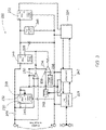
- FIG. 3 is a system block diagram of a power management circuit 222, not falling under the scope of claim 1.
- the power management circuit 222 can be used in any of a variety of process control systems such as illustrated in FIGS. 1 and 2 , among other systems.
- the power management circuit 222 can be electrically connected between nodes LIP and LIN to facilitate the flow of loop current through the power management circuit 222 when the nodes LIP and LIN are connected in series with the loop wires 208a and 208b.
- the flow of loop current through the power management circuit 222 and can induce an insertion voltage across nodes LIP and LIN. Conventionally, this insertion voltage is insufficient to power the wireless adapter device 220.
- the power management circuit 222 can include a voltage converter 228 connected to the insertion voltage at an input 230.
- An output 232 of the voltage converter 228 can be connected with certain electronic components of the wireless adapter device 220 such as an amplifier 234, a current loop amplifier 250, a HART interface logic device 225, and a microcontroller 247.
- the voltage converter 228 can convert the insertion voltage to an appropriate source voltage for powering each of the electronic components of the wireless adapter device 220.
- the power management circuit 222 can include a wireless communication device 224.
- the wireless communication device 224 can be configured to provide wireless RF communications to transmit information (e.g., process variable information) between the wireless adapter device 220 and an RF based network in a facility.
- the wireless communication device 224 can include a transceiver that is supportive of any of a variety of wireless platforms such as IEEE 802.11, Bluetooth, microwave, infrared, or the like.
- the power management circuit 222 can further include HART interface logic 225 associated with the wireless communication device 224 to facilitate communication according to a HART protocol.
- the wired-HART protocol communicates digital data between devices such as field devices 102 and controllers 112 using Frequency Shift Keying (FSK).
- FSK Frequency Shift Keying
- the HART interface logic 225 can communicate with the field devices 102 and controllers 112 using the wired-HART protocol, while the associated wireless communication device 224 can communicate with a WirelessHart network.
- the power available from the loop current (e.g., insertion power) to power the wireless communication device 224 is generally the multiplicative product of the loop current and the insertion voltage.
- the wireless communication device 224 consumes more instantaneous power than is available as insertion power.
- the power management circuit 222 can include an electrical storage element device 226 that is configured to store insertion power and deliver the stored insertion power to the wireless communication device 224 as needed.
- the electrical storage device 226 is illustrated in FIG. 3 to comprise a supercapacitor, it will be appreciated that, any of a variety of alternative suitable electrical storage devices can be provided such as a general purpose energy storage capacitor or a battery, for example.
- the electrical storage device 226 can be charged by a second voltage converter 244. As illustrated in FIG. 3 , the electrical storage device 226 can be in electrical communication with output OUT of the second voltage converter 244. The second voltage converter 244 can transfer substantially all of the insertion power available, less the power consumed by the first voltage regulator 232, to charge the electrical storage device 226. Electrical energy can be provided from the electrical storage device 226 to meet the instantaneous and long term power requirements of the wireless communication device 224.
- the storage capacity of the electrical storage device 226 can be many times greater than the insertion power such that charging of the electrical storage device 226 can take a relatively long period of time (potentially ranging from about one minute to a few hours).
- the voltage (e.g., radio voltage) of the electrical storage device 226 can also become depleted.
- the power management circuit 222 can include a third voltage converter 252 that is in electrical communication with each of the electrical storage device 226 and the wireless communication device 224.
- the third voltage converter 252 can generate a constant regulated radio voltage regardless of whether the electrical storage device 226 is charged to maximum capacity or is nearly depleted.
- the insertion voltage has been regulated to a desired setpoint with a current shunt provided in parallel with the power management circuit 222.
- loop current is divided between the power management circuit 222 and the current shunt (e.g., a current divider circuit). If the loop current changes (e.g., due to a changing process variable), the current through the current shunt correspondingly changes to maintain the balance between the current shunt and the power management circuit thereby maintaining a constant insertion voltage drop. It will be appreciated however that any current that flows through the current shunt is not available to power the wireless adapter device and is wasted.
- the second voltage converter 244 can be configured to regulate the insertion voltage without the need for a conventional-type current shunt.
- voltage converters maintain a consistent voltage level at their output by varying the power transferred from their input.
- this conventional voltage regulator configuration is suitable where there is ample power provided at the input (e.g., to satisfy the power demands of a circuit electrically connected to the output of the voltage regulator).
- the current and power provided at the input e.g., input power
- a conventional voltage converter configuration may transfer too much power to the output thereby reducing the voltage at the input.
- the second voltage converter 244 can be configured as a power converter to sense and control the insertion voltage at the input 230 and to balance the insertion power with the power transferred into the electrical storage device 226.
- the insertion voltage can be compared with a reference voltage to regulate the insertion voltage.
- the amplifier 234 can be in communication with a feedback input FB of the second voltage converter.
- a reference voltage is shown to be connected to a positive input 238 of the amplifier 234.
- a variable scaler 242 can be connected to a negative input 236 of the amplifier 234.
- the insertion voltage can be provided to the amplifier 234 through the variable scaler 242 and the amplifier 234 can compare it to the reference voltage.
- the amplifier 234 can provide a control signal to the feedback input FB to regulate the insertion voltage to the reference voltage. It will be appreciated, however, that a power converter can be provided in any of a variety of suitable alternative arrangements to maintain an insertion voltage drop at a particular level.
- the power management circuit 222 is therefore configured to control the insertion voltage while allowing full loop current (less the miniscule current consumed by the other circuits) to flow to the electrical storage device 226 (e.g., to power the wireless adapter device 220).
- the second voltage converter 244 can overcome some of the shortcomings of using a conventional current shunt to regulate the insertion voltage.
- the insertion power (less the miniscule power consumed by the other circuits) generated from the insertion voltage and the loop current can be delivered to the electrical storage device 226.
- the loop current changes (e.g., when a control process variable changes)
- the change in power is transmitted to the electrical storage device 226 via the second voltage converter 244 (e.g., the power management circuit 222 can track and adapt in real-time).
- the power management circuit 222 can be configured as an "Energy Pump" circuit which converts the insertion voltage to a higher voltage and can also charge the electrical storage device 226 to a higher voltage. Since the precise amount of energy transfer is monitored and compared against a reference voltage (e.g., by the amplifier 234) the insertion voltage can be precise (DC voltage) and stable (AC noise) during the operation of the field device 202. It will also be appreciated that the power extracted from the insertion voltage can be regulated to maintain the loop insertion voltage at a constant value.
- the variable scaler 242 can vary the voltage provided to the negative input 236 of the amplifier 234 to facilitate selective control of the insertion voltage.
- the power provided to the electrical storage device 226 can change when the loop current changes (e.g., when the process variable changes). For example, when the loop current increases, the insertion voltage can be increased to increase the insertion power provided to the electrical storage device 226.
- the electrical storage device 226 can be charged quickly thereby increasing the power available from the electrical storage device 226 for operating the wireless communication device 224.
- the variable scaler 242 can therefore be controlled to maximize the insertion power provided to the electrical storage device 226.
- the power management circuit 222 can provide more power to the electrical storage device 226 than would be available from a conventional current shunting system (e.g., 3.5 mW). If the loop current increases to 20mA, the power management circuit 222 can generate 20mW of insertion power, without the variable scaler 242 changing the 1VDC insertion voltage.
- the power management circuit 222 can generate about 50mW of insertion power which, in some instances, is enough to power the wireless communication device 224 directly (e.g., without first charging the electrical storage device 226). It will be appreciated that a power management circuit can be configured to handle any of a variety of insertion voltages (e.g., 0.5VDC, over 2.5VDC).
- the power management circuit 222 can include a microcontroller 247 coupled with the variable scaler 242.
- the microcontroller 247 can control the variable scaler 242 based upon a predefined setpoint.
- the microcontroller 247 can control the variable scaler 242 dynamically (e.g., according to an algorithm).
- the microcontroller 247 can include a microprocessor, an arithmetic logic unit, or any of a variety of other suitable electronic components.
- any of a variety of additional or alternative components can facilitate control of the variable scaler 242.
- the setpoint can be configured at time of installation, or can be dynamically configured such as with the microcontroller 247 or across a wireless communication network by a host system as required or desired.
- the insertion voltage drop induced by the flow of current through the power management circuit 222 can provide an additional voltage drop to the process control system 200.
- the magnitude of the insertion drop voltage should be such, that when the insertion drop voltage is combined with the other voltage losses in the process control system 200, the voltage of the power supply 214 is not exceeded.
- the combined voltage losses across the loop wires 208a, 208b, 210a, 210b, the wireless adapter device 220, the field device 202, and the current sense resistor 218 should be maintained at or below the voltage of the power supply 214.
- the voltage of the power supply 214 and corresponding voltage losses can vary for different process control system configurations.
- the insertion voltage drop on a power management circuit 222 is permanently set at a low level (e.g., about 1 VDC) in order to ensure compatibility with various process control system configurations.
- these conventional power management circuits 222 are provided on a process control system with low cumulative voltage losses, insertion power can be lost. For example, if the power supply 214 can supply about a 5 VDC voltage, and the combined voltage losses of a process control system (ignoring the insertion voltage drop) total about 2 VDC, the process control system can accept an insertion voltage drop of up to about 3 VDC.
- the power management circuit 222 can be configured to control the insertion voltage drop (e.g., stabilize, regulate) to maximize the insertion power for any of a variety of process control system configurations.
- a voltage shunting circuit can be provided in communication with the electrical storage device 226.
- the voltage shunting circuit can be configured to prevent an overvoltage condition within the electrical storage device 226.
- a voltage shunt 246 can be provided in parallel with the electrical storage device 226, such that as the electrical storage device 226 reaches capacity, the voltage shunt 246 can bypass current and power to prevent the voltage across the electrical storage device 226 from further increasing.
- the power delivered from the output of the second voltage converter 244 (less the miniscule power consumed by the other circuits) can be shunted by the voltage shunt 246 to balance the power and regulate the voltage across the electrical storage device 226.
- the voltage shunt 246 can cease shunting until the electrical storage device 226 is at capacity again.
- a stable voltage can be provided from the insertion voltage drop.
- a third voltage converter 252 can be provided to create a constant regulated control voltage to power certain electronic components of FIG. 3 .
- the power management circuit 222 can provide fast deployment that allows the application of loop currents in excess of the loop current normal operating ranges (e.g., about 3.5-20mA, up to about 130mA). This fast deployment can allow a user installing wireless adapter device 220 to rapidly charge the electrical storage device to provide minimal delay after installation to power the wireless communication device 224.
- the power management circuit 222 includes a fast deployment circuit configured to sense a magnitude of the loop current, and when the magnitude of the loop current reaches a threshold value, maintain the voltage level at the input at an elevated level to facilitate a substantial increase in the charging power delivered to the electrical storage device 226.
- the power management circuit 222 can include a sense resistor 248 and a loop current amplifier 250.
- the microcontroller 247 can monitor the loop current across the sense resistor 248 and compare it with a threshold value. When the magnitude of the loop current exceeds the threshold value, the microcontroller 247 can define a setpoint for maximum insertion voltage with using the variable scaler 242, and the power management circuit 222 can then receive maximum insertion power. In one embodiment, the microcontroller 247can compare the loop current against a threshold value of 25mA. When the loop current exceeds 25mA for a period of time the variable scaler 242 can be set to provide a maximum insertion voltage drop.
- the power management circuit 222 can include over-current protection. This over current protection can limit the amount of insertion power when an excessive amount of loop current is being provided to the power management circuit 222.
- the power management circuit 222 can include an over current protection circuit configured to sense the magnitude of the loop current and, when the magnitude of the loop current reaches an over-current threshold value, disable the second voltage converter 244.
- over current protection circuit can include the sense resistor 248 and the loop current amplifier 250. The positive input and negative input of the loop current amplifier 250 can be electrically connected on opposite sides of the sense resistor 248 to monitor the magnitude of the loop current.
- the output of the loop current amplifier can provide a signal to shut down the second voltage converter 244 thereby limiting the insertion power provided to the power management circuit 222.
- the loop current amplifier 250 can compare the loop current against about a 130mA threshold. When the loop current exceeds 130mA, the loop current amplifier 250 can provide a signal to shut down the second voltage converter 244.
- the power management circuit 222 can include a power save capability.
- the power management circuit 222 can monitor the loop current (e.g., through sense resistor 248). If the magnitude of the loop current is reduced to a negligible amount, the power management circuit 222 can power down all significant power consuming circuits to preserve the power stored in the electrical storage device 226. When the loop current regains a particular magnitude (e.g., greater than a negligible amount), the power management circuit 222 can return power to the circuits that were previously shut down. If a process control system has a power outage, this function can help ensure that the wireless adapter device 220 will be immediately available with the electrical storage device 226 at capacity when power returns. If a user has pre-charged the wireless adapter device 220 (e.g., in a lab), this feature can ensure that the wireless adapter device 220 will be fully powered and immediately available to begin radio communications when it is installed on a process control system.
- the power management circuit 222 can include an instant-on function, whereby an auxiliary power is established to power the internal control circuitry before the electrical storage device 226 charges up.
- the power management circuit 222 can include dynamic radio duty cycle management.
- the power management circuit 222 can inform a wireless communication network of the insertion power available to power the wireless communication device 224. Accordingly, the wireless communication network can dynamically configure a maximum radio duty cycle to match the insertion power available to power the wireless communication device 224.
- a duty cycle can be increased to achieve faster update rates for changing process variables.
- the duty cycle can be reduced to ensure that the power demand by the wireless communication network does not exhaust the storage capacity of the electrical storage device 226 thereby causing an ultimately loss of radio communication until the electrical storage device 226 can be recharged.
- the power management system 400 includes many of the elements presented and described for the power management circuit 222 presented in FIG. 3 and described in the above accompanying text. Therefore, for clarity of exposition, the differences between the elements of FIG. 3 and FIG. 4 are described below.
- the power management circuit 402 of the power management system 400 includes an energy pump 404 having an input 405 in electrical communication with the LIP 422 connector, a feedback input 403 for accepting a feedback sense from a control circuit, and an output 406 that provides a charging voltage to an energy storage element 226 and a voltage regulator 252.
- the energy pump 404 is a voltage converter that receives a first voltage and converts it to a higher (or lower) voltage.
- the energy pump 404 is selectively controlled by the control circuit 410 that modulates the feedback sense.
- the control circuit 410 comprises a feedback amplifier 407 that has two inputs 236, 238 connected to a reference voltage 237 and the output of a scaler 408.
- the control circuit 410 modulates the feedback sense at least in part based on the loop current in the control loop to regulate the insertion voltage between LIP 422 and LIN 424.
- the scaler 408 facilitates control of the insertion voltage by the microcontroller 247. This allows dynamic control of power management by the power management circuit 402.
- the loop insertion voltage can be regulated by balancing the energy extracted from the control loop with the energy available in the control loop. Because the current regulator 116 modulates the current in the control loop, for example between 4 mA and 20 mA, the amount of energy available in the control loop can change dynamically.
- the precise amount of energy transfer by the energy pump 404 is monitored by the feedback amplifier 407 that compares the reference voltage 237 against the insertion voltage and keeps the insertion voltage precise (DC voltage) and stable (AC noise.) No power from the control loop is wasted until the stored power in the energy storage element 226 reaches a maximum, resulting in efficient utilization of the available power in the control loop.
- the scaler 408 can be dynamically controlled by the microcontroller 247.
- the insertion voltage can be set to a higher than normal value, for example 2.5 Volts. Setting the insertion voltage higher enables a rapid deployment mode, whereby the energy storage element 226 can be quickly charged to full capacity. Setting the insertion voltage higher enables the energy pump 404 to transfer more power from the control loop. More power can be available from the energy pump 404 and energy storage element 226, and the microcontroller 247 can increase the radio 224 transmission parameters, increasing the transmission rate and enabling more frequent communications across the radio link.
- IS intrinsically safe
- the increased amount of power can allow the microcontroller 247 to run at a second operational mode, such as a high power mode.
- the scaler 408 can be a step-volt scaler, enabling insertion voltages at incremental steps between approximately 0.5 Volts and approximately 2.5 Volts in 0.5 Volt increments.
- the scaler 408 can be a digital or analogy scaler, enabling insertion voltages at various ranges and increments.
- the power management circuit 402 is connected in serial with a control loop of a controller 112, 212 and a field device 102, 202 (shown in FIG. 1 and FIG. 3 ). In this configuration, the power management circuit 402 is connected in serial with one of the control loop wires 108, 110, 208, 210 using the LIP 422 and LIN 424 connectors, as illustrated in FIG.2 .
- the power management circuit 402 can also be connected with a battery (not shown) that directly powers the field device 102, 202. In this configuration, there is no controller 112, 212. Instead, a first terminal of a battery, for example the positive terminal, is connected to the direct power input 420. The second terminal of the battery, for example the negative terminal, is connected to the LIN 424 connector. The first terminal of the battery is also connected to one of the connection terminals 104 of the field device 102. The other connection terminal 106 is in electrical communication with the HART connector 426.
- Current for the control loop flows from the first terminal of the battery through the field device 102, is modulated by current regulator 116, that can also be a voltage or power regulator, and returns to the power management circuit 402 through the HART connector 426, through the internal current sense resistor 418 and field device switch 416, and through the sense resistor 248 to the second terminal of the battery.
- current regulator 116 that can also be a voltage or power regulator
- the sense resistor 248 is a loop sense resistor in that it provides a way to produce a measurement of the amount of loop current in the control loop or current loop.
- the sense resistor 248 can be a low value resistor, for example a 1 Ohm resistor with a 1/4 Watt power rating.
- a loop current sense amplifier 409 connects to the sense resistor 248 and produces a loop current sense signal from the voltage drop, or loop current sense value, across the sense resistor 248.
- the loop current sense signal can be provided to the microcontroller 247.
- the loop current sense amplifier 409 can be connected through a blocking diode 413 to the feedback input 413 of the energy pump 404 to further modulate the feedback sense.
- a high value in the loop current sense signal indicates an unsafe or over-current condition for the power management circuit 402.
- the high value in the loop current sense signal can be configured to have a threshold that, when exceeded, shuts down the energy pump to prevent damage to the power management circuit 402.
- the voltage drop across the sense resistor 248 provides a loop current sense value directly correlating to the current in the control loop passing through the power management circuit 402 between the L1N 424 connector and L1P 422 connector.
- the current passing through the sense resistor 248 includes both the current in the control loop and the current drawn from the battery by the power management circuit 402.
- the microcontroller 247 selectively turns on and off the voltage converter 414. Note that the microcontroller 247 can be any kind of processor, CPU, ASIC, or processing logic and analog-to-digital converters, or combination of circuits.
- the voltage converter 414 When the voltage converter 414 is turned on, the voltage converter 414 provides an electric charging current directly to the energy storage element 226 and voltage regulator 252. A blocking diode 413 prevents power from flowing back into the voltage converter 414, for example when the energy pump 404 is turned on. The amount of current and power drawn by the voltage converter 414 is dependent upon the current draw of the power consuming circuits 225, 247, 224. For example, if the radio 224 is transmitting and receiving wireless data, the radio 224 can draw electrical power from the stored power in energy storage element 226 through the voltage regulator 252. In response, the voltage converter 414 can draw power from the battery to recharge the energy storage element 226 or to directly provide charging voltage to the voltage regulator 252.
- the electrical return to the battery for the current drawn by both the power management circuit 402 and the power consuming circuits 225, 247, 224 is through the sense resistor 248. Therefore, when the microcontroller 247 selectively turns on the voltage converter 414, the sense resistor provides a measure of the total consumption of power by the power management system 400 and field device.
- the energy storage element 226 is the source of electrical power for both the power management circuit 402 and the power consuming circuits 225, 247, 224.
- the voltage regulator 252 is off, the power management circuit 402 and power consuming circuits 225, 247, 224 are electrically isolated from the control loop and the sense resistor 248.
- the current flowing through the sense resistor 248 is the current in the control loop.
- the controller 247 can selectively turn on and off the voltage converter 414, perform measurements of the current flowing through the sense resistor 248, and obtain a diagnostic indication of the power usage in the power management system 400.
- the controller can 247 monitor the loop current flowing through the sense resistor 248 and selectively turn off components to reduce or disable the loop current.
- the controller 247 can disable the radio 224, the HART communications interface 225, and the voltage converter 414, and the controller 247 can also create an open circuit condition in the field device switch 416.
- the controller 247 can open the field device switch 416 if there is an electrical fault in the control loop, or if the power management circuit 402 is incorrectly connected to the battery or field device 102, 202.
- the controller can open the field device switch 416 to prevent damage to the power management system 400 in the event of a reverse connection of the battery, or an overvoltage condition, significantly reducing field return failures of components damaged by incorrect installation.
- the field device switch 416 can default to being open, allowing installation prior to powering the controller 247. Once powered, the controller 247 can momentarily close the field device switch 416 to test for incorrect connections or voltages without subjecting the rest of the power management circuit 402 to significant amounts of current.
- the field device switch 416 provides a current return path for the control loop through the internal current sense resistor 418, or current sense resistor.
- the internal current sense resistor 418 can be 250 Ohms.
- An internal current sense resistor 418 having a resistance of 250 Ohms provides the proper impedance characteristics for transmitting and receiving HART communications between the HART communications interface logic 225 and the field device 102, 202.
- the HART communications interface logic 225 is capacitively connected to the control loop.
- the capacitor 412 blocks the DC component of the while passing the FSK signal of the HART protocol. Note that the capacitor 412 can be connected to any point in the control loop.
- the controller 247 can open the field device switch 416 to remove power to the field device 102, 202 thereby placing the field device 102, 202 in a sleep mode.
- the controller 247 can close the field device switch 416 and wake the field device 102, 202 to retrieve the required information. Selectively removing power to the field device 102, 202 can substantially lengthen the useful life of a battery.
- the power management system 400 can intermittently and briefly power up the field device 102, 202 through the field device switch 416, communicate with the field device 102, 202 to obtain a control process data, power down the field device 102, 202, and send the data or information across a wireless network.
Landscapes
- Engineering & Computer Science (AREA)
- Power Engineering (AREA)
- Charge And Discharge Circuits For Batteries Or The Like (AREA)
- Arrangements For Transmission Of Measured Signals (AREA)
Description
- The systems and methods relate generally to the field of process control systems. More specifically, the disclosed systems and methods relate to devices, systems and methods for transmitting and receiving telemetry data with field devices that utilize process control loops.
- Conventional process control systems generally include basic components for sensing, measuring, evaluating, and adjusting or otherwise controlling a variety of process variables. Additionally, common systems include components that provide means for communicating information about process control variables between sensing, measuring, or adjusting components and evaluation components. One such system for communicating information is a two-wire system that creates a loop that physically connects a sensing, measuring, evaluating, or adjusting device to a controller.
- Sensing, measuring, evaluating, and/or adjusting devices in industrial production environments are generally referred to as field devices. Field devices commonly sense or monitor one or more process control variables such as temperature, pressure, or rate of fluid flow, among others. Many of these field devices can communicate information about the sensed or monitored variable to a process controller by regulating electrical current on the two-wire system. The controller in this type of environment can sense the electrical current, such as by using a current sense resistor, and translate the sensed magnitude of the current, as well as any sensed change of the current, into information about the sensed or monitored control variable. Many common field devices can receive information from the controller and effect changes or adjustments to the sensed or monitored control.
- Two methods of communicating information using a multi-wire loop system include analog signaling methods, such as communicating information via an analog current signal, and digital signaling methods that can communicate information as a frequency shift keyed carrier signal which can be superimposed on, and coexist with, an analog signaling method on the multi-wire loop. One digital signaling method is the Highway Addressable Remote Transducer ("HART") communications protocol from the HART® Communication Foundation. As referred to herein, HART refers to any past or present version of the HART protocol, including Wireless HART, variants of such versions, as well as any future version that may be created so long as those future versions are compatible or can be modified to be compatible with the systems and methods disclosed herein.
-
WO 2008/157391 A1 discloses a method of scavenging power in a circuit having a power source generating electric current including connecting a power scavenging device having an input terminal pair and an output terminal pair to the circuit via the input terminal pair, dynamically regulating a voltage drop across the input terminal pair of the power scavenging device, harvesting electrical energy available at the regulated voltage drop from the electric current flowing through the first imputer terminal pair of the power scavenging device, and providing the harvested electrical energy at the output terminal pair of the power scavenging device. -
WO 2008/157389 A1 discloses a bidirectional DC to DC converter having a first operational mode and a second operational mode includes a first terminal pair that has a positive terminal and a negative terminal and that connects the converter to a first electrical circuit, a second terminal pair that has a positive terminal and a negative terminal and that connects the converter to a second electric circuit, an accumulation element for temporary accumulation of electric energy; and a switching circuit connected to the first terminal pair, the second terminal pair, and the accumulation element. Electric energy is transferred from the first electric circuit to the second electric circuit via the accumulation element in the first operational mode of the bidirectional DC to DC converter and, from the second electric circuit to the first electric circuit via the accumulation element in the second operational mode of the DC to DC converter. -
US 2009/146502 A1 discloses a power management circuit including a power regulator and a wireless communication device. -
US 2009/309558 A1 discloses a wireless adapter for use in a two-wire process control loop including wireless communication circuitry and first and second terminals configured to couple in series with the two-wire process control loop. -
US 2005/0289276 A1 discloses a field device for use in an industrial process control or monitoring system, including terminals configured to connect to a two-wire process control loop. - The scope of protection is defined by the independent claims. Advantageous embodiments are given by the dependent claims.
- While the specification concludes with claims particularly pointing out and distinctly claiming the present invention, it is believed that the same will be better understood from the following description taken in conjunction with the accompanying drawings in which:
-
FIG. 1 is a system block diagram of a process control loop not falling under the scope of claim 1; -
FIG. 2 is a system block diagram of a process control loop; and -
FIG. 3 is a system block diagram of a power management circuit, not falling under the socpe of claim 1; and -
FIG. 4 is a system block diagram of a power management system. - Most components and methods disclosed are described with reference to the drawings. In drawings, like reference numbers are used to refer to like elements throughout the drawings. In the following description, to aid in explanation, a number of specific details are provided to promote understanding of the disclosed subject matter. It may be evident, however, that certain of these specific details can be omitted or combined with others in a specific implementation. In other instances, certain structures and devices are shown in block diagram form in order to facilitate description. Further, it should be noted that although specific examples presented can include or reference specific components, a specific implementation of the components and methods disclosed and described is not necessarily limited to those specific examples and can be employed in other contexts as well. Those of ordinary skill in the art will readily recognize that the disclosed and described components and methods can be used to create other components and execute other methods in a wide variety of ways.
-
FIG. 1 is a system block diagram of aprocess control system 100, not falling under the scope of claim 1. As illustrated, afield device 102 can includeconnection terminals control loop wires controller 112 can include apower supply 114 that is operable to supply electrical current (e.g., loop current) and voltage to thecontrol loop wires power supply 114 can be in electrical communication with thecontrol loop wire 108 and a negative terminal of thepower supply 114 can be in electrical communication with thecontrol loop wire 110. Thepower supply 114 can produce loop current magnitudes levels from approximately 3.5mA to approximately 20mA during normal operation, with maximum current values as high as approximately 130mA during maximum fault conditions. However, any of a variety of other current or voltage ranges may be provided by the power supply, such as may correspond with voltage and current parameters for a particular field device, for example. - As illustrated in
FIG. 1 , thefield device 102 can include acurrent regulator 116 that is operable to change amounts of loop current provided through thecontrol loop wires current regulator 116, thefield device 102 can regulate the amounts of electrical current to communicate a control process variable to thecontroller 112. For example, if thefield device 102 is configured to sense temperature, thecurrent regulator 116 can regulate the amounts of current provided through thecontrol loop wires - In order to communicate the amount of current to the
controller 112, thecontroller 112 can include acurrent sense resistor 118 which can operate to sense the loop current provided through thecontrol loop wires controller 112 can sense loop current or other variables in any of a variety of suitable alternative configurations. Additionally or alternatively, theprocess control system 100 can include digital signaling components (not shown) to facilitate the communication of information as a carrier signal on thecontrol loop wires field device 102 can include Highway Addressable Remote Transducer ("HART") communication components, such as wireless HART communication components. However, the process control system can include components for any of a variety of suitable alternative communication protocols such as, for example, ISA SP100 and Fieldbus among others. - It will be appreciated that the
process control system 100 can communicate with an associated network to provide information to a host controller. Conventionally, thecontroller 112 communicates with the associated network via wired communication. However, in some embodiments, thecontroller 112 may not support wired communication with the network (e.g., when digital signaling equipment is not present on thecontroller 112 or during failure of certain digital signaling equipment). Therefore, in one embodiment, as illustrated inFIG. 2 , awireless adapter device 220 is included. As will be described in more detail below, thewireless adapter device 220 can include components and circuitry that are configured to provide wireless radio frequency ("RF") communications with an RF-based network in a facility that can communicate with acontroller 212 or other suitable controllers. Thewireless adapter device 220 can function as a gateway between components that can provide digital signaling for afield device 202 and a wireless communication network (not shown) in a facility. Thecontroller 212 can be thecontroller 112 ofFIG. 1 or as another suitable controller. Thefield device 202 can be thefield device 102 depicted and described inFIG. 1 or can be another suitable field device. - Conventionally, the
wireless adapter device 220 can be powered by dedicated power sources such as, for example, a separate wired power circuit, a battery, or a solar power cell, among others. However, installation and maintenance of awireless adapter device 220 powered by these dedicated power sources can be costly and time consuming. Therefore, as illustrated inFIG. 2 , thewireless adapter device 220 is provided in electrical communication with thecontrol loop wires wireless adapter device 220 is powered from loop current through thecontrol loop wires wireless adapter device 220 includes apower management circuit 222 provided between nodes LIP and L1N which is connected in series with thecontrol loop wires power management circuit 222 to power thewireless adapter device 220 without substantially interfering with the loop current. Accordingly, thewireless adapter device 220 can be powered by theprocess control system 200 without hindering thefield device 202 from communicating a control process variable to the controller 212 (e.g., via current onloop wires -
FIG. 3 is a system block diagram of apower management circuit 222, not falling under the scope of claim 1. It will be appreciated that, thepower management circuit 222 can be used in any of a variety of process control systems such as illustrated inFIGS. 1 and 2 , among other systems. Thepower management circuit 222 can be electrically connected between nodes LIP and LIN to facilitate the flow of loop current through thepower management circuit 222 when the nodes LIP and LIN are connected in series with theloop wires power management circuit 222 and can induce an insertion voltage across nodes LIP and LIN. Conventionally, this insertion voltage is insufficient to power thewireless adapter device 220. Therefore, thepower management circuit 222 can include avoltage converter 228 connected to the insertion voltage at aninput 230. Anoutput 232 of thevoltage converter 228 can be connected with certain electronic components of thewireless adapter device 220 such as anamplifier 234, acurrent loop amplifier 250, a HARTinterface logic device 225, and amicrocontroller 247. Thevoltage converter 228 can convert the insertion voltage to an appropriate source voltage for powering each of the electronic components of thewireless adapter device 220. - The
power management circuit 222 can include awireless communication device 224. Thewireless communication device 224 can be configured to provide wireless RF communications to transmit information (e.g., process variable information) between thewireless adapter device 220 and an RF based network in a facility. In certain embodiments, thewireless communication device 224 can include a transceiver that is supportive of any of a variety of wireless platforms such as IEEE 802.11, Bluetooth, microwave, infrared, or the like. In addition, thepower management circuit 222 can further includeHART interface logic 225 associated with thewireless communication device 224 to facilitate communication according to a HART protocol. - Referring again to
FIG. 1 and continuing to refer toFIG. 2 , the wired-HART protocol communicates digital data between devices such asfield devices 102 andcontrollers 112 using Frequency Shift Keying (FSK). FSK is a modulation that is superimposed on top of the lower frequency analog control signal, namely the 4-20ma signal commonly used by industrial measurement devices. This allows digital communications betweendevices HART interface logic 225 can communicate with thefield devices 102 andcontrollers 112 using the wired-HART protocol, while the associatedwireless communication device 224 can communicate with a WirelessHart network. - It will be appreciated that the power available from the loop current (e.g., insertion power) to power the
wireless communication device 224 is generally the multiplicative product of the loop current and the insertion voltage. Typically, thewireless communication device 224 consumes more instantaneous power than is available as insertion power. Thepower management circuit 222 can include an electricalstorage element device 226 that is configured to store insertion power and deliver the stored insertion power to thewireless communication device 224 as needed. Although theelectrical storage device 226 is illustrated inFIG. 3 to comprise a supercapacitor, it will be appreciated that, any of a variety of alternative suitable electrical storage devices can be provided such as a general purpose energy storage capacitor or a battery, for example. - The
electrical storage device 226 can be charged by a second voltage converter 244. As illustrated inFIG. 3 , theelectrical storage device 226 can be in electrical communication with output OUT of the second voltage converter 244. The second voltage converter 244 can transfer substantially all of the insertion power available, less the power consumed by thefirst voltage regulator 232, to charge theelectrical storage device 226. Electrical energy can be provided from theelectrical storage device 226 to meet the instantaneous and long term power requirements of thewireless communication device 224. - It will be appreciated that the storage capacity of the
electrical storage device 226 can be many times greater than the insertion power such that charging of theelectrical storage device 226 can take a relatively long period of time (potentially ranging from about one minute to a few hours). When the stored insertion power from theelectrical storage device 226 becomes depleted, the voltage (e.g., radio voltage) of theelectrical storage device 226 can also become depleted. To optimize the delivery of the stored insertion power from theelectrical storage device 226 at a substantially constant voltage, thepower management circuit 222 can include athird voltage converter 252 that is in electrical communication with each of theelectrical storage device 226 and thewireless communication device 224. Thethird voltage converter 252 can generate a constant regulated radio voltage regardless of whether theelectrical storage device 226 is charged to maximum capacity or is nearly depleted. - Conventionally, the insertion voltage has been regulated to a desired setpoint with a current shunt provided in parallel with the
power management circuit 222. In such an arrangement, loop current is divided between thepower management circuit 222 and the current shunt (e.g., a current divider circuit). If the loop current changes (e.g., due to a changing process variable), the current through the current shunt correspondingly changes to maintain the balance between the current shunt and the power management circuit thereby maintaining a constant insertion voltage drop. It will be appreciated however that any current that flows through the current shunt is not available to power the wireless adapter device and is wasted. - The second voltage converter 244 can be configured to regulate the insertion voltage without the need for a conventional-type current shunt. In some conventional configurations, voltage converters maintain a consistent voltage level at their output by varying the power transferred from their input. Generally, this conventional voltage regulator configuration is suitable where there is ample power provided at the input (e.g., to satisfy the power demands of a circuit electrically connected to the output of the voltage regulator). However, when the current and power provided at the input (e.g., input power) is limited, as is the case with the loop current into the
power management circuit 222, and the demand on the output is higher than the input power, as is the case with theelectrical storage device 226, a conventional voltage converter configuration may transfer too much power to the output thereby reducing the voltage at the input. - The second voltage converter 244, therefore, can be configured as a power converter to sense and control the insertion voltage at the
input 230 and to balance the insertion power with the power transferred into theelectrical storage device 226. In one embodiment, the insertion voltage can be compared with a reference voltage to regulate the insertion voltage. For example, as illustrated inFIG. 3 , theamplifier 234 can be in communication with a feedback input FB of the second voltage converter. A reference voltage is shown to be connected to apositive input 238 of theamplifier 234. Avariable scaler 242 can be connected to anegative input 236 of theamplifier 234. The insertion voltage can be provided to theamplifier 234 through thevariable scaler 242 and theamplifier 234 can compare it to the reference voltage. Theamplifier 234 can provide a control signal to the feedback input FB to regulate the insertion voltage to the reference voltage. It will be appreciated, however, that a power converter can be provided in any of a variety of suitable alternative arrangements to maintain an insertion voltage drop at a particular level. - The
power management circuit 222 is therefore configured to control the insertion voltage while allowing full loop current (less the miniscule current consumed by the other circuits) to flow to the electrical storage device 226 (e.g., to power the wireless adapter device 220). Accordingly, the second voltage converter 244 can overcome some of the shortcomings of using a conventional current shunt to regulate the insertion voltage. For example, the insertion power (less the miniscule power consumed by the other circuits) generated from the insertion voltage and the loop current can be delivered to theelectrical storage device 226. When the loop current changes (e.g., when a control process variable changes), the change in power is transmitted to theelectrical storage device 226 via the second voltage converter 244 (e.g., thepower management circuit 222 can track and adapt in real-time). - It will be appreciated that the
power management circuit 222 can be configured as an "Energy Pump" circuit which converts the insertion voltage to a higher voltage and can also charge theelectrical storage device 226 to a higher voltage. Since the precise amount of energy transfer is monitored and compared against a reference voltage (e.g., by the amplifier 234) the insertion voltage can be precise (DC voltage) and stable (AC noise) during the operation of thefield device 202. It will also be appreciated that the power extracted from the insertion voltage can be regulated to maintain the loop insertion voltage at a constant value. - The
variable scaler 242 can vary the voltage provided to thenegative input 236 of theamplifier 234 to facilitate selective control of the insertion voltage. By controlling the insertion voltage, the power provided to theelectrical storage device 226 can change when the loop current changes (e.g., when the process variable changes). For example, when the loop current increases, the insertion voltage can be increased to increase the insertion power provided to theelectrical storage device 226. By increasing the insertion power, theelectrical storage device 226 can be charged quickly thereby increasing the power available from theelectrical storage device 226 for operating thewireless communication device 224. - The
variable scaler 242 can therefore be controlled to maximize the insertion power provided to theelectrical storage device 226. In one example, for a field device (e.g., 202) that is configured to operate at a 1 Volt DC ("VDC") insertion voltage and at a minimum of 3.5 mA, thepower management circuit 222 can provide more power to theelectrical storage device 226 than would be available from a conventional current shunting system (e.g., 3.5 mW). If the loop current increases to 20mA, thepower management circuit 222 can generate 20mW of insertion power, without thevariable scaler 242 changing the 1VDC insertion voltage. However, if the variable scaler varies the insertion voltage to about 2.5 VDC, then thepower management circuit 222 can generate about 50mW of insertion power which, in some instances, is enough to power thewireless communication device 224 directly (e.g., without first charging the electrical storage device 226). It will be appreciated that a power management circuit can be configured to handle any of a variety of insertion voltages (e.g., 0.5VDC, over 2.5VDC). - In one embodiment, as illustrated in
FIG. 3 , thepower management circuit 222 can include amicrocontroller 247 coupled with thevariable scaler 242. In one embodiment, themicrocontroller 247 can control thevariable scaler 242 based upon a predefined setpoint. In another embodiment, themicrocontroller 247 can control thevariable scaler 242 dynamically (e.g., according to an algorithm). It will be appreciated that themicrocontroller 247 can include a microprocessor, an arithmetic logic unit, or any of a variety of other suitable electronic components. However, any of a variety of additional or alternative components can facilitate control of thevariable scaler 242. It will be appreciated that the setpoint can be configured at time of installation, or can be dynamically configured such as with themicrocontroller 247 or across a wireless communication network by a host system as required or desired. - It will be appreciated that the insertion voltage drop induced by the flow of current through the
power management circuit 222 can provide an additional voltage drop to theprocess control system 200. When thewireless adapter device 220 is connected between nodes LIP and LIN, the magnitude of the insertion drop voltage should be such, that when the insertion drop voltage is combined with the other voltage losses in theprocess control system 200, the voltage of thepower supply 214 is not exceeded. For example, the combined voltage losses across theloop wires wireless adapter device 220, thefield device 202, and thecurrent sense resistor 218 should be maintained at or below the voltage of thepower supply 214. - It will be appreciated that the voltage of the
power supply 214 and corresponding voltage losses can vary for different process control system configurations. Conventionally, the insertion voltage drop on apower management circuit 222 is permanently set at a low level (e.g., about 1 VDC) in order to ensure compatibility with various process control system configurations. However, if these conventionalpower management circuits 222 are provided on a process control system with low cumulative voltage losses, insertion power can be lost. For example, if thepower supply 214 can supply about a 5 VDC voltage, and the combined voltage losses of a process control system (ignoring the insertion voltage drop) total about 2 VDC, the process control system can accept an insertion voltage drop of up to about 3 VDC. However, if the insertion voltage drop of the conventional power management circuit has been set at about 1 VDC, the insertion power will be comparatively less than a conventional management circuit having an insertion voltage drop of about 3 VDC. Therefore, thepower management circuit 222 can be configured to control the insertion voltage drop (e.g., stabilize, regulate) to maximize the insertion power for any of a variety of process control system configurations. - It will be appreciated that as the
electrical storage device 226 reaches maximum capacity, the voltage across theelectrical storage device 226 can rise above proper operating limits. Rather than shunting current and power away from the power management circuit 222 (e.g., with a current shunt), a voltage shunting circuit can be provided in communication with theelectrical storage device 226. The voltage shunting circuit can be configured to prevent an overvoltage condition within theelectrical storage device 226. In one embodiment, as illustrated inFIG. 3 , avoltage shunt 246 can be provided in parallel with theelectrical storage device 226, such that as theelectrical storage device 226 reaches capacity, thevoltage shunt 246 can bypass current and power to prevent the voltage across theelectrical storage device 226 from further increasing. In such an embodiment, the power delivered from the output of the second voltage converter 244 (less the miniscule power consumed by the other circuits) can be shunted by thevoltage shunt 246 to balance the power and regulate the voltage across theelectrical storage device 226. As power is delivered from theelectrical storage device 226 to thewireless communication device 224, thevoltage shunt 246 can cease shunting until theelectrical storage device 226 is at capacity again. - It will be appreciated to power various components of the
power management circuit 222, a stable voltage can be provided from the insertion voltage drop. In one embodiment, as illustrated inFIG. 3 , athird voltage converter 252 can be provided to create a constant regulated control voltage to power certain electronic components ofFIG. 3 . - The
power management circuit 222 can provide fast deployment that allows the application of loop currents in excess of the loop current normal operating ranges (e.g., about 3.5-20mA, up to about 130mA). This fast deployment can allow a user installingwireless adapter device 220 to rapidly charge the electrical storage device to provide minimal delay after installation to power thewireless communication device 224. To facilitate this fast deployment, thepower management circuit 222 includes a fast deployment circuit configured to sense a magnitude of the loop current, and when the magnitude of the loop current reaches a threshold value, maintain the voltage level at the input at an elevated level to facilitate a substantial increase in the charging power delivered to theelectrical storage device 226. In one embodiment, thepower management circuit 222 can include asense resistor 248 and a loopcurrent amplifier 250. Themicrocontroller 247 can monitor the loop current across thesense resistor 248 and compare it with a threshold value. When the magnitude of the loop current exceeds the threshold value, themicrocontroller 247 can define a setpoint for maximum insertion voltage with using thevariable scaler 242, and thepower management circuit 222 can then receive maximum insertion power. In one embodiment, the microcontroller 247can compare the loop current against a threshold value of 25mA. When the loop current exceeds 25mA for a period of time thevariable scaler 242 can be set to provide a maximum insertion voltage drop. - The
power management circuit 222 can include over-current protection. This over current protection can limit the amount of insertion power when an excessive amount of loop current is being provided to thepower management circuit 222. To facilitate over-current protection thepower management circuit 222 can include an over current protection circuit configured to sense the magnitude of the loop current and, when the magnitude of the loop current reaches an over-current threshold value, disable the second voltage converter 244. In one embodiment, over current protection circuit can include thesense resistor 248 and the loopcurrent amplifier 250. The positive input and negative input of the loopcurrent amplifier 250 can be electrically connected on opposite sides of thesense resistor 248 to monitor the magnitude of the loop current. If the loop current exceeds a maximum threshold, the output of the loop current amplifier can provide a signal to shut down the second voltage converter 244 thereby limiting the insertion power provided to thepower management circuit 222. In one embodiment, the loopcurrent amplifier 250 can compare the loop current against about a 130mA threshold. When the loop current exceeds 130mA, the loopcurrent amplifier 250 can provide a signal to shut down the second voltage converter 244. - The
power management circuit 222 can include a power save capability. Thepower management circuit 222 can monitor the loop current (e.g., through sense resistor 248). If the magnitude of the loop current is reduced to a negligible amount, thepower management circuit 222 can power down all significant power consuming circuits to preserve the power stored in theelectrical storage device 226. When the loop current regains a particular magnitude (e.g., greater than a negligible amount), thepower management circuit 222 can return power to the circuits that were previously shut down. If a process control system has a power outage, this function can help ensure that thewireless adapter device 220 will be immediately available with theelectrical storage device 226 at capacity when power returns. If a user has pre-charged the wireless adapter device 220 (e.g., in a lab), this feature can ensure that thewireless adapter device 220 will be fully powered and immediately available to begin radio communications when it is installed on a process control system. - The
power management circuit 222 can include an instant-on function, whereby an auxiliary power is established to power the internal control circuitry before theelectrical storage device 226 charges up. - The
power management circuit 222 can include dynamic radio duty cycle management. In particular, thepower management circuit 222 can inform a wireless communication network of the insertion power available to power thewireless communication device 224. Accordingly, the wireless communication network can dynamically configure a maximum radio duty cycle to match the insertion power available to power thewireless communication device 224. When the insertion power is elevated, a duty cycle can be increased to achieve faster update rates for changing process variables. However, when the insertion power is depleted, the duty cycle can be reduced to ensure that the power demand by the wireless communication network does not exhaust the storage capacity of theelectrical storage device 226 thereby causing an ultimately loss of radio communication until theelectrical storage device 226 can be recharged. - Referring now to
FIG. 4 and continuing to refer toFIG. 1 and FIG. 2 , apower management system 400 according to an embodiment is presented. Thepower management system 400 includes many of the elements presented and described for thepower management circuit 222 presented inFIG. 3 and described in the above accompanying text. Therefore, for clarity of exposition, the differences between the elements ofFIG. 3 andFIG. 4 are described below. - The
power management circuit 402 of thepower management system 400 includes anenergy pump 404 having aninput 405 in electrical communication with theLIP 422 connector, afeedback input 403 for accepting a feedback sense from a control circuit, and anoutput 406 that provides a charging voltage to anenergy storage element 226 and avoltage regulator 252. Theenergy pump 404 is a voltage converter that receives a first voltage and converts it to a higher (or lower) voltage. Theenergy pump 404 is selectively controlled by thecontrol circuit 410 that modulates the feedback sense. Thecontrol circuit 410 comprises afeedback amplifier 407 that has twoinputs reference voltage 237 and the output of ascaler 408. Thecontrol circuit 410 modulates the feedback sense at least in part based on the loop current in the control loop to regulate the insertion voltage betweenLIP 422 andLIN 424. - The
scaler 408 facilitates control of the insertion voltage by themicrocontroller 247. This allows dynamic control of power management by thepower management circuit 402. The loop insertion voltage can be regulated by balancing the energy extracted from the control loop with the energy available in the control loop. Because thecurrent regulator 116 modulates the current in the control loop, for example between 4 mA and 20 mA, the amount of energy available in the control loop can change dynamically. The precise amount of energy transfer by theenergy pump 404 is monitored by thefeedback amplifier 407 that compares thereference voltage 237 against the insertion voltage and keeps the insertion voltage precise (DC voltage) and stable (AC noise.) No power from the control loop is wasted until the stored power in theenergy storage element 226 reaches a maximum, resulting in efficient utilization of the available power in the control loop. - The
scaler 408 can be dynamically controlled by themicrocontroller 247. In some applications, for example if there is no intrinsically safe (IS) barrier in the control loop, the insertion voltage can be set to a higher than normal value, for example 2.5 Volts. Setting the insertion voltage higher enables a rapid deployment mode, whereby theenergy storage element 226 can be quickly charged to full capacity. Setting the insertion voltage higher enables theenergy pump 404 to transfer more power from the control loop. More power can be available from theenergy pump 404 andenergy storage element 226, and themicrocontroller 247 can increase theradio 224 transmission parameters, increasing the transmission rate and enabling more frequent communications across the radio link. The increased amount of power can allow themicrocontroller 247 to run at a second operational mode, such as a high power mode. Thescaler 408 can be a step-volt scaler, enabling insertion voltages at incremental steps between approximately 0.5 Volts and approximately 2.5 Volts in 0.5 Volt increments. Thescaler 408 can be a digital or analogy scaler, enabling insertion voltages at various ranges and increments. - The
power management circuit 402 is connected in serial with a control loop of acontroller field device 102, 202 (shown inFIG. 1 andFIG. 3 ). In this configuration, thepower management circuit 402 is connected in serial with one of thecontrol loop wires LIP 422 andLIN 424 connectors, as illustrated inFIG.2 . - The
power management circuit 402 can also be connected with a battery (not shown) that directly powers thefield device controller direct power input 420. The second terminal of the battery, for example the negative terminal, is connected to theLIN 424 connector. The first terminal of the battery is also connected to one of theconnection terminals 104 of thefield device 102. Theother connection terminal 106 is in electrical communication with theHART connector 426. Current for the control loop flows from the first terminal of the battery through thefield device 102, is modulated bycurrent regulator 116, that can also be a voltage or power regulator, and returns to thepower management circuit 402 through theHART connector 426, through the internalcurrent sense resistor 418 andfield device switch 416, and through thesense resistor 248 to the second terminal of the battery. - The
sense resistor 248 is a loop sense resistor in that it provides a way to produce a measurement of the amount of loop current in the control loop or current loop. To minimize voltage drop across thesense resistor 248, thesense resistor 248 can be a low value resistor, for example a 1 Ohm resistor with a 1/4 Watt power rating. A loopcurrent sense amplifier 409 connects to thesense resistor 248 and produces a loop current sense signal from the voltage drop, or loop current sense value, across thesense resistor 248. The loop current sense signal can be provided to themicrocontroller 247. The loopcurrent sense amplifier 409 can be connected through a blockingdiode 413 to thefeedback input 413 of theenergy pump 404 to further modulate the feedback sense. In this configuration, a high value in the loop current sense signal indicates an unsafe or over-current condition for thepower management circuit 402. The high value in the loop current sense signal can be configured to have a threshold that, when exceeded, shuts down the energy pump to prevent damage to thepower management circuit 402. - When the
power management circuit 402 is connect in serial with a control loop, the voltage drop across thesense resistor 248 provides a loop current sense value directly correlating to the current in the control loop passing through thepower management circuit 402 between theL1N 424 connector andL1P 422 connector. When thepower management circuit 402 is utilizing the battery, the current passing through thesense resistor 248 includes both the current in the control loop and the current drawn from the battery by thepower management circuit 402. Themicrocontroller 247 selectively turns on and off thevoltage converter 414. Note that themicrocontroller 247 can be any kind of processor, CPU, ASIC, or processing logic and analog-to-digital converters, or combination of circuits. When thevoltage converter 414 is turned on, thevoltage converter 414 provides an electric charging current directly to theenergy storage element 226 andvoltage regulator 252. A blockingdiode 413 prevents power from flowing back into thevoltage converter 414, for example when theenergy pump 404 is turned on. The amount of current and power drawn by thevoltage converter 414 is dependent upon the current draw of thepower consuming circuits radio 224 is transmitting and receiving wireless data, theradio 224 can draw electrical power from the stored power inenergy storage element 226 through thevoltage regulator 252. In response, thevoltage converter 414 can draw power from the battery to recharge theenergy storage element 226 or to directly provide charging voltage to thevoltage regulator 252. The electrical return to the battery for the current drawn by both thepower management circuit 402 and thepower consuming circuits sense resistor 248. Therefore, when themicrocontroller 247 selectively turns on thevoltage converter 414, the sense resistor provides a measure of the total consumption of power by thepower management system 400 and field device. - When the
voltage converter 414 is turned off, theenergy storage element 226 is the source of electrical power for both thepower management circuit 402 and thepower consuming circuits voltage regulator 252 is off, thepower management circuit 402 andpower consuming circuits sense resistor 248. The current flowing through thesense resistor 248 is the current in the control loop. Thecontroller 247 can selectively turn on and off thevoltage converter 414, perform measurements of the current flowing through thesense resistor 248, and obtain a diagnostic indication of the power usage in thepower management system 400. The controller can 247 monitor the loop current flowing through thesense resistor 248 and selectively turn off components to reduce or disable the loop current. For example, thecontroller 247 can disable theradio 224, theHART communications interface 225, and thevoltage converter 414, and thecontroller 247 can also create an open circuit condition in thefield device switch 416. - By opening, or electrically opening, the
field device switch 416, power to thefield device controller 247 can open thefield device switch 416 if there is an electrical fault in the control loop, or if thepower management circuit 402 is incorrectly connected to the battery orfield device field device switch 416 to prevent damage to thepower management system 400 in the event of a reverse connection of the battery, or an overvoltage condition, significantly reducing field return failures of components damaged by incorrect installation. Thefield device switch 416 can default to being open, allowing installation prior to powering thecontroller 247. Once powered, thecontroller 247 can momentarily close thefield device switch 416 to test for incorrect connections or voltages without subjecting the rest of thepower management circuit 402 to significant amounts of current. - The
field device switch 416 provides a current return path for the control loop through the internalcurrent sense resistor 418, or current sense resistor. The internalcurrent sense resistor 418 can be 250 Ohms. An internalcurrent sense resistor 418 having a resistance of 250 Ohms provides the proper impedance characteristics for transmitting and receiving HART communications between the HARTcommunications interface logic 225 and thefield device communications interface logic 225 is capacitively connected to the control loop. Thecapacitor 412 blocks the DC component of the while passing the FSK signal of the HART protocol. Note that thecapacitor 412 can be connected to any point in the control loop. - The
controller 247 can open thefield device switch 416 to remove power to thefield device field device controller 247 requires information from thefield device controller 247 can close thefield device switch 416 and wake thefield device field device radio 224, thepower management system 400 can intermittently and briefly power up thefield device field device switch 416, communicate with thefield device field device - The foregoing description of embodiments and examples has been presented for purposes of illustration and description. It is not intended to be exhaustive or limiting to the forms described. Numerous modifications are possible in light of the above teachings. Some of those modifications have been discussed and others will be understood by those skilled in the art.
- The embodiments were chosen and described for illustration of various embodiments. The scope is, of course, not limited to the examples or embodiments set forth herein, but can be employed in any number of applications and equivalent devices by those of ordinary skill in the art. Rather it is hereby intended the scope be defined by the claims appended hereto.
Claims (12)
- A system, comprising:- a field device (102, 202);- a battery as a power supply (214) electrically connected to the field device (102, 202), the power supply (214) being configured to transmit a loop current to the field device (102, 202) and the field device (102, 202) being configured to regulate the loop current, and- a wireless communication device (224) electrically connected to a power management circuit (222) and configured to receive electrical power from the power management circuit (222),- a plurality of nodes (L1N, L1P), the nodes being connected in series with control loop wiresfor connection in series with the current loop for serial connection with the field device (102, 202)- the-power management circuit (222) connectable between the plurality of nodes (L1N, L1P), and configured to be in a serial connection between the power supply (214) and the field device (102, 202) a flow of loop current through the power management circuit (222) inducing a regulated voltage drop across the nodes (L1N, L1P) at an insertion voltage, the power management circuit (222) configured to output an electrical power derived from the insertion voltage, wherein the field device (102, 202) is configured to receive a DC voltage from the battery,the power management circuit (222) comprising:- an energy pump (404) configured to convert voltage to a higher or lower voltage, the energy pump (404) configured to input at least a portion of the insertion voltage, the energy pump (404) configured to receive a feedback input, the energy pump (404) configured to output a charging voltage based at least in part on the feedback input, the charging voltage configured to source the electrical power output by the power management circuit (222);- an electrical storage element (226) electrically connected to the energy pump (404), the electrical storage element (226) configured to store the charging voltage as a stored power,- a voltage regulator (252) electrically connected to the electrical storage element (226), the voltage regulator (252) configured to regulate the stored power and output the electrical power of the power management circuit (222) and- a control circuit (410) configured to regulate the insertion voltage by modulating the feedback input to the energy pump (404), the control circuit (410) configured to modulate the feedback input at least partially in response to an electrical change in the current loop;characterized in that the power management circuit (222) further comprises:- a voltage converter (414) configured to input the DC voltage from the battery and output the charging voltage to the power management circuit (222);- wherein the voltage converter and a first terminal of the field device are electrically connected to a first terminal of the battery, and wherein- the power management circuit further comprises a loop sense resistor(248) electrically connected to a second terminal of the battery, the loop sense resistor (248) configured to provide a loop current sense of a current in the power management circuit (222); and- a loop current sense amplifier (409) configured to receive loop current sense, and output a loop current sense signal;- a current sense resistor (418) electrically connected to a second terminal of the field device (102, 202);- a processor (247), forming part of a power consuming circuit (225,247, 224) and electrically connected to the loop sense resistor (248) as well as the voltage converter (414), the processor (247) configured to receive the loop current sense signal and to selectively turn on and turn off the voltage converter (414) and such that when the voltage converter (414) is turned off the current in the power management circuit (222) is approximately a loop current of the battery in series with the field device (102, 202), the loop sense resistor (248), and the current sense resistor (418); and- the power consuming circuit (225, 247, 224) configured to receive the electrical power from the power management circuit (222).
- The system of claim 1, wherein the power consuming circuit (225, 247, 224) is further selected from the group consisting of a wireless communication device (224) and a Highway Addressable Remote Transducer, HART, interface configured to communicate with the field device (102, 202) according to a HART protocol.
- The system of claim 1, wherein the electrical storage element (226) comprises at least one of a capacitor and a battery.
- The system of claim 1, wherein the power management circuit (222) further comprises: a voltage shunting circuit (246) electrically connected to the electrical storage element (226), the voltage shunting circuit configured to prevent an overvoltage condition for the electrical storage element (226).
- The system of claim 1, wherein the control circuit (410) further comprises: a feedback amplifier (407) configured to output the feedback input to the energy pump (404), comprising: a first input (238) configured to receive a reference voltage (237); a second input (236) configured to receive a feedback voltage having a value correlating to a multiple of the Insertion voltage; and, an output electrically connected to the energy pump (404).
- The system of claim 5, wherein the control circuit (410) further comprises:
a scaler (108) configured to input at least a portion of the insertion voltage and output, to the second input (236) of the feedback amplifier (407), a feedback voltage that is a selectable multiple of the insertion voltage, and wherein the processor (247) is configured to control the scaler (108). - The system of claim 5,
wherein the loop current sense amplifier (409) is electrically connected to the energy pump (404), and wherein the loop current sense signal further modulates the feedback input to disable the energy pump (404) when the current in the power management circuit (222) exceeds an over-current threshold, and wherein the loop current sense amplifier (409) is configured to provide a loop current sense signal corresponding to a loop current in the current loop, and wherein the processor (247) is electrically connected to the loop current sense amplifier (409), the processor (247) is configured to receive the loop current sense signal, and wherein the processor (247) is configured to operate in a fast-deployment mode by controlling the scaler (108) and increasing the insertion voltage when a value of the loop current sense signal crosses a threshold. - The system of claim 1, wherein the control circuit (410) is configured to regulate the about 0.5 Volts Direct Current and about 2.5 Volts Direct Current and further comprising:a HART interface configured to communicate with the field device (102, 202) according to a HART protocol, the HART interface configured to be capacitively coupled to the current loop;a field device switch (416) configured to selectively create an open circuit condition for the current sense resistor (418), and wherein the processor (247) is configured to control the field device switch (416) to selectively create the open circuit condition for the current sense resistor (418).
- The system of claim 8, wherein the field device (102, 202) comprises a voltage transducer.
- The system of claim 9, further comprising: the HART interface (225) configured to be capacitively coupled to the current loop, and wherein the power supply (214) is a battery.
- A method for managing power of a system according to claim 1 comprising a field device (102, 202) and a wireless communication device (224), the method comprising: receiving a DC voltage from a battery, the battery is configured to provide a loop current to the field device (102, 202); converting the DC voltage to a charging voltage, wherein the converting is selectively disabled during an operation of measuring a loop current of the field device (102, 202); delivering the charging voltage to an electrical storage element (226); and, storing the charging voltage as a stored power in the electrical storage element (226) for delivery to the wireless communication device (224).
- The method of claim 11, further comprising: disabling the loop current to place the field device (102, 202) in a sleep mode; and,
enabling the loop current to wake the field device (102, 202), and further comprising:measuring the loop current; and,disabling the loop current when the loop current exceeds a threshold, and further comprising regulating the stored power that is delivered from the electrical storage element (226) to the wireless communication device (224), and further comprising:
communicating a process control data with the field device (102, 202) using a HART protocol, and further comprising:
communicating the process control data with a gateway using the wireless communication device (224).
Applications Claiming Priority (2)
| Application Number | Priority Date | Filing Date | Title |
|---|---|---|---|
| US31703110P | 2010-03-24 | 2010-03-24 | |
| PCT/US2011/029877 WO2011119892A1 (en) | 2010-03-24 | 2011-03-24 | Power management circuit for a wireless communication device and process control system using same |
Publications (3)
| Publication Number | Publication Date |
|---|---|
| EP2567436A1 EP2567436A1 (en) | 2013-03-13 |
| EP2567436A4 EP2567436A4 (en) | 2015-10-07 |
| EP2567436B1 true EP2567436B1 (en) | 2022-04-20 |
Family
ID=44673642
Family Applications (1)
| Application Number | Title | Priority Date | Filing Date |
|---|---|---|---|
| EP11760264.9A Active EP2567436B1 (en) | 2010-03-24 | 2011-03-24 | Power management circuit for a wireless communication device and process control system using same |
Country Status (4)
| Country | Link |
|---|---|
| US (2) | US9735570B2 (en) |
| EP (1) | EP2567436B1 (en) |
| CN (1) | CN103380556B (en) |
| WO (1) | WO2011119892A1 (en) |
Families Citing this family (28)
| Publication number | Priority date | Publication date | Assignee | Title |
|---|---|---|---|---|
| JP2012027832A (en) * | 2010-07-27 | 2012-02-09 | Yokogawa Electric Corp | Field device |
| US20120253481A1 (en) * | 2011-03-29 | 2012-10-04 | General Electric Company | Hart channel interface component including redundancy |
| JP2014112819A (en) | 2012-10-30 | 2014-06-19 | Yokogawa Electric Corp | Radio equipment, input/output unit, radio unit and radio equipment setup method |
| DE102012112635A1 (en) * | 2012-12-19 | 2014-06-26 | Endress+Hauser Process Solutions Ag | Radio module for a field device |
| WO2014146243A1 (en) * | 2013-03-19 | 2014-09-25 | General Electric Company | Current loop voltage modulator for communication interface |
| JP5898642B2 (en) * | 2013-05-20 | 2016-04-06 | 横河電機株式会社 | Wireless equipment |
| US9008197B2 (en) | 2013-07-26 | 2015-04-14 | General Electric Company | Current loop voltage modulator for communication interface |
| US20150194809A1 (en) * | 2014-01-07 | 2015-07-09 | Erick Mendoza | Variable DC Power Supply and HART Adapter |
| US10281939B2 (en) | 2014-02-17 | 2019-05-07 | Commscope Technologies Llc | Methods and equipment for reducing power loss in cellular systems |
| US9448576B2 (en) | 2014-02-17 | 2016-09-20 | Commscope Technologies Llc | Programmable power supplies for cellular base stations and related methods of reducing power loss in cellular systems |
| US11333695B2 (en) | 2014-02-17 | 2022-05-17 | Commscope Technologies Llc | Methods and equipment for reducing power loss in cellular systems |
| US9575132B2 (en) * | 2014-07-17 | 2017-02-21 | Honeywell International Inc. | Method and system for calculating accurate battery percentage usage in wireless field devices |
| US10862535B2 (en) * | 2014-08-28 | 2020-12-08 | General Electric Company | Methods, systems, and devices for coupling a modulated voltage signal to a current loop using a variable impedance bridge |
| US10110279B2 (en) * | 2014-10-07 | 2018-10-23 | Endress + Hauser Process Solutions Ag | Apparatus for supplying power to a field device |
| KR102341489B1 (en) * | 2015-02-27 | 2021-12-21 | 삼성전자 주식회사 | Electronic device and method for charging controlling of the electronic device |
| US9615149B1 (en) * | 2015-10-26 | 2017-04-04 | Honeywell International Inc. | Process interface including wireless multi-loop single hop device |
| US10599134B2 (en) * | 2016-07-22 | 2020-03-24 | Fisher-Rosemount Systems, Inc. | Portable field maintenance tool configured for multiple process control communication protocols |
| SE1750548A1 (en) * | 2017-05-05 | 2018-11-06 | Fingerprint Cards Ab | Field-powered biometric device, and method of controlling a field-powered biometric device |
| KR101984140B1 (en) * | 2017-05-12 | 2019-05-30 | 주식회사 맵스 | Wireless Power Receiver Unit using charge pump power stage |
| DE102017114851A1 (en) * | 2017-07-04 | 2019-01-10 | Endress+Hauser SE+Co. KG | Field device adapter for wireless data transmission |
| DE102017121923B4 (en) * | 2017-09-21 | 2019-12-19 | Vega Grieshaber Kg | Measuring arrangement with an operating device and method for operating such a measuring arrangement |
| US10531255B2 (en) | 2017-10-17 | 2020-01-07 | Honeywell International Inc. | Method and system for over-the-air provisioning of wireless HART (highway addressable remote transducer) devices |
| DE102018120108A1 (en) * | 2018-08-17 | 2020-02-20 | Endress+Hauser SE+Co. KG | Field device of automation technology |
| DE102018122014A1 (en) | 2018-09-10 | 2020-03-12 | Endress + Hauser Flowtec Ag | Measuring system and measuring arrangement thus formed |
| US10892925B2 (en) * | 2018-11-16 | 2021-01-12 | Analog Devices International Unlimited Company | Communication receiver interface for current loop circuit |
| DE102019119840A1 (en) * | 2019-07-23 | 2021-01-28 | Endress+Hauser SE+Co. KG | Field device of automation technology |
| CN114552529B (en) * | 2022-01-28 | 2022-10-21 | 绵阳惠科光电科技有限公司 | Overvoltage protection circuit, overvoltage protection device, display panel and display |
| DE102022119145A1 (en) * | 2022-07-29 | 2024-02-01 | Endress+Hauser Flowtec Ag | Connection circuit for a field device and field device |
Family Cites Families (31)
| Publication number | Priority date | Publication date | Assignee | Title |
|---|---|---|---|---|
| KR100285949B1 (en) | 1996-12-12 | 2001-04-16 | 윤종용 | Battery charging circuit |
| US6167134A (en) * | 1997-04-22 | 2000-12-26 | Silicon Laboratories, Inc. | External resistor and method to minimize power dissipation in DC holding circuitry for a communication system |
| US5959372A (en) | 1997-07-21 | 1999-09-28 | Emerson Electric Co. | Power management circuit |
| US6870279B2 (en) | 1998-01-05 | 2005-03-22 | Capstone Turbine Corporation | Method and system for control of turbogenerator power and temperature |
| US6304978B1 (en) | 1998-11-24 | 2001-10-16 | Intel Corporation | Method and apparatus for control of the rate of change of current consumption of an electronic component |
| GB2357381B (en) | 1999-12-13 | 2003-12-24 | Sony Uk Ltd | Changing the output frequency of a phased-locked loop |
| US6574515B1 (en) | 2000-05-12 | 2003-06-03 | Rosemount Inc. | Two-wire field-mounted process device |
| EP1202145B1 (en) | 2000-10-27 | 2005-02-09 | Invensys Systems, Inc. | Field device with a transmitter and/ or receiver for wireless data communication |
| WO2003036777A1 (en) | 2001-10-22 | 2003-05-01 | Apple Computer, Inc. | Methods and apparatus for charging a battery in a peripheral device |
| US6842383B2 (en) * | 2003-01-30 | 2005-01-11 | Saifun Semiconductors Ltd. | Method and circuit for operating a memory cell using a single charge pump |
| US7194363B2 (en) * | 2003-12-22 | 2007-03-20 | Endress + Hauser Flowtec Ag | Ultrasonic flowmeter |
| EP1721067B1 (en) | 2004-03-02 | 2010-01-06 | Rosemount, Inc. | Process device with improved power generation |
| US8538560B2 (en) | 2004-04-29 | 2013-09-17 | Rosemount Inc. | Wireless power and communication unit for process field devices |
| US8145180B2 (en) * | 2004-05-21 | 2012-03-27 | Rosemount Inc. | Power generation for process devices |
| US7262693B2 (en) | 2004-06-28 | 2007-08-28 | Rosemount Inc. | Process field device with radio frequency communication |
| US8160535B2 (en) * | 2004-06-28 | 2012-04-17 | Rosemount Inc. | RF adapter for field device |
| JP4792851B2 (en) * | 2004-11-01 | 2011-10-12 | 横河電機株式会社 | Field equipment |
| US8050624B2 (en) | 2005-06-24 | 2011-11-01 | Rosemount, Inc. | Distributed process control system and method utilizing wireless communication of packet messages |
| JP4676000B2 (en) * | 2005-06-27 | 2011-04-27 | ローズマウント インコーポレイテッド | Field device with dynamically adjustable power consumption radio frequency communication |
| CN101243532B (en) * | 2005-08-18 | 2012-01-18 | 电子线技术院株式会社 | Detector for electron column and method for detecting electrons for electron column |
| US7230528B2 (en) | 2005-09-20 | 2007-06-12 | Lawrence Kates | Programmed wireless sensor system |
| DE102005047894B4 (en) * | 2005-10-06 | 2010-05-12 | Abb Ag | Method for checking the operability of transmitters |
| EP1798835B1 (en) * | 2005-12-13 | 2009-12-30 | Research In Motion Limited | Charger and power supply for mobile devices |
| CN101730968B (en) | 2007-06-15 | 2014-08-20 | 费希尔控制产品国际有限公司 | Input regulated DC to DC converter for power scavenging |
| RU2476978C2 (en) * | 2007-06-15 | 2013-02-27 | Фишер Контролз Интернешнел Ллс | Bidirectional converter of dc into dc to control energy accumulator when taking energy |
| US8280317B2 (en) | 2007-06-26 | 2012-10-02 | Mark Sinreich | Pass-through connection systems and methods for process control field devices |
| US8258749B2 (en) | 2007-06-26 | 2012-09-04 | Mark Sinreich | Power regulator for use with wireless communication device |
| US20090094466A1 (en) * | 2007-10-04 | 2009-04-09 | Matthew Kerry R | Process field device with augmented loop power and wireless communication |
| WO2009154748A2 (en) * | 2008-06-17 | 2009-12-23 | Rosemount Inc. | Rf adapter for field device with low voltage intrinsic safety clamping |
| WO2009154756A1 (en) | 2008-06-17 | 2009-12-23 | Rosemount Inc. | Rf adapter for field device with variable voltage drop |
| WO2011116362A1 (en) * | 2010-03-18 | 2011-09-22 | Kenneth Burns | Frequency shift keying modulation and demodulation |
-
2011
- 2011-03-24 US US13/699,107 patent/US9735570B2/en active Active
- 2011-03-24 EP EP11760264.9A patent/EP2567436B1/en active Active
- 2011-03-24 WO PCT/US2011/029877 patent/WO2011119892A1/en active Application Filing
- 2011-03-24 CN CN201180026086.XA patent/CN103380556B/en active Active
-
2017
- 2017-07-07 US US15/644,251 patent/US10554043B2/en active Active
Also Published As
| Publication number | Publication date |
|---|---|
| CN103380556B (en) | 2016-02-03 |
| US9735570B2 (en) | 2017-08-15 |
| WO2011119892A1 (en) | 2011-09-29 |
| EP2567436A4 (en) | 2015-10-07 |
| US10554043B2 (en) | 2020-02-04 |
| CN103380556A (en) | 2013-10-30 |
| EP2567436A1 (en) | 2013-03-13 |
| US20170331286A1 (en) | 2017-11-16 |
| US20130082667A1 (en) | 2013-04-04 |
Similar Documents
| Publication | Publication Date | Title |
|---|---|---|
| US10554043B2 (en) | Power management circuit for wireless communication device and process control system using same | |
| US9625895B2 (en) | Regulating power for a wireless communication device | |
| US9860093B2 (en) | Frequency shift keying modulation and demodulation | |
| US9818530B2 (en) | Adaptive wireless power transfer system and method | |
| US20090207770A1 (en) | Apparatus and method for power management of wirelessly networked devices | |
| KR20180018741A (en) | Adapter and charge control method | |
| US20080222431A1 (en) | Power Adapter Capable of Communicating Digitally with Electronic Devices | |
| US9883257B2 (en) | Smart grid appliance control | |
| WO2012007942A2 (en) | Power management system and method for an inductive power transfer system | |
| CA2761979A1 (en) | Circuit and method for ultra-low idle power | |
| US10566833B2 (en) | External battery backup unit | |
| EP3796504B1 (en) | Electrical system and method of operating such a system | |
| CN213754015U (en) | Charging circuit, charging box and charging system of bluetooth headset | |
| KR20190012985A (en) | A method for controlling a wireless power transmitter and a wireless power transmitter | |
| CN215731396U (en) | Internet of things switching circuit applied to automatic change-over switch | |
| JP2016103890A (en) | Power control unit and power control system | |
| US11921532B2 (en) | Controlling pulsed operation of a power supply during a power outage | |
| ES2664468T3 (en) | Power management circuit for a wireless communication device and a procedure control system that uses the same | |
| US20240154445A1 (en) | Intelligent bms charge control | |
| US10931139B1 (en) | Emergency battery packs for low voltage systems | |
| Kondratjevs et al. | Development of power supply management module for radio signal repeaters of automatic metering reading system in variable solar density conditions | |
| RU2574318C2 (en) | Wireless field device having detachable power supply | |
| CN114421434A (en) | Constant temperature and constant current control system, circuit and linear charger |
Legal Events
| Date | Code | Title | Description |
|---|---|---|---|
| PUAI | Public reference made under article 153(3) epc to a published international application that has entered the european phase |
Free format text: ORIGINAL CODE: 0009012 |
|
| 17P | Request for examination filed |
Effective date: 20121218 |
|
| AK | Designated contracting states |
Kind code of ref document: A1 Designated state(s): AL AT BE BG CH CY CZ DE DK EE ES FI FR GB GR HR HU IE IS IT LI LT LU LV MC MK MT NL NO PL PT RO RS SE SI SK SM TR |
|
| RAP1 | Party data changed (applicant data changed or rights of an application transferred) |
Owner name: MACTEK CORPORATION |
|
| RIN1 | Information on inventor provided before grant (corrected) |
Inventor name: MACTEK CORPORATION |
|
| DAX | Request for extension of the european patent (deleted) | ||
| RA4 | Supplementary search report drawn up and despatched (corrected) |
Effective date: 20150904 |
|
| RIC1 | Information provided on ipc code assigned before grant |
Ipc: H02J 1/00 20060101ALI20150831BHEP Ipc: H02J 1/10 20060101AFI20150831BHEP Ipc: H02M 3/158 20060101ALI20150831BHEP Ipc: H02J 7/34 20060101ALI20150831BHEP |
|
| RAP1 | Party data changed (applicant data changed or rights of an application transferred) |
Owner name: PEPPERL+FUCHS GMBH |
|
| RIN1 | Information on inventor provided before grant (corrected) |
Inventor name: PEPPERL+FUCHS GMBH |
|
| STAA | Information on the status of an ep patent application or granted ep patent |
Free format text: STATUS: EXAMINATION IS IN PROGRESS |
|
| 17Q | First examination report despatched |
Effective date: 20180920 |
|
| RAP1 | Party data changed (applicant data changed or rights of an application transferred) |
Owner name: PEPPERL+FUCHS AG |
|
| RIN1 | Information on inventor provided before grant (corrected) |
Inventor name: PEPPERL+FUCHS AG |
|
| STAA | Information on the status of an ep patent application or granted ep patent |
Free format text: STATUS: EXAMINATION IS IN PROGRESS |
|
| RAP1 | Party data changed (applicant data changed or rights of an application transferred) |
Owner name: PEPPERL+FUCHS SE |
|
| RIN1 | Information on inventor provided before grant (corrected) |
Inventor name: PEPPERL+FUCHS SE |
|
| STAA | Information on the status of an ep patent application or granted ep patent |
Free format text: STATUS: EXAMINATION IS IN PROGRESS |
|
| REG | Reference to a national code |
Ref country code: DE Ref legal event code: R079 Ref document number: 602011072782 Country of ref document: DE Free format text: PREVIOUS MAIN CLASS: H02J0001100000 Ipc: H02J0001060000 |
|
| GRAP | Despatch of communication of intention to grant a patent |
Free format text: ORIGINAL CODE: EPIDOSNIGR1 |
|
| STAA | Information on the status of an ep patent application or granted ep patent |
Free format text: STATUS: GRANT OF PATENT IS INTENDED |
|
| RIC1 | Information provided on ipc code assigned before grant |
Ipc: G05B 19/042 20060101ALN20220125BHEP Ipc: H02J 7/34 20060101ALI20220125BHEP Ipc: H02J 1/10 20060101ALI20220125BHEP Ipc: H02J 1/06 20060101AFI20220125BHEP |
|
| GRAS | Grant fee paid |
Free format text: ORIGINAL CODE: EPIDOSNIGR3 |
|
| RIC1 | Information provided on ipc code assigned before grant |
Ipc: G05B 19/042 20060101ALN20220128BHEP Ipc: H02J 7/34 20060101ALI20220128BHEP Ipc: H02J 1/10 20060101ALI20220128BHEP Ipc: H02J 1/06 20060101AFI20220128BHEP |
|
| INTG | Intention to grant announced |
Effective date: 20220214 |
|
| GRAA | (expected) grant |
Free format text: ORIGINAL CODE: 0009210 |
|
| STAA | Information on the status of an ep patent application or granted ep patent |
Free format text: STATUS: THE PATENT HAS BEEN GRANTED |
|
| RIN1 | Information on inventor provided before grant (corrected) |
Inventor name: SINREICH, MARK |
|
| AK | Designated contracting states |
Kind code of ref document: B1 Designated state(s): AL AT BE BG CH CY CZ DE DK EE ES FI FR GB GR HR HU IE IS IT LI LT LU LV MC MK MT NL NO PL PT RO RS SE SI SK SM TR |
|
| REG | Reference to a national code |
Ref country code: GB Ref legal event code: FG4D |
|
| REG | Reference to a national code |
Ref country code: CH Ref legal event code: EP |
|
| REG | Reference to a national code |
Ref country code: DE Ref legal event code: R096 Ref document number: 602011072782 Country of ref document: DE |
|
| REG | Reference to a national code |
Ref country code: IE Ref legal event code: FG4D |
|
| REG | Reference to a national code |
Ref country code: AT Ref legal event code: REF Ref document number: 1485957 Country of ref document: AT Kind code of ref document: T Effective date: 20220515 |
|
| REG | Reference to a national code |
Ref country code: LT Ref legal event code: MG9D |
|
| REG | Reference to a national code |
Ref country code: NL Ref legal event code: MP Effective date: 20220420 |
|
| REG | Reference to a national code |
Ref country code: AT Ref legal event code: MK05 Ref document number: 1485957 Country of ref document: AT Kind code of ref document: T Effective date: 20220420 |
|
| PG25 | Lapsed in a contracting state [announced via postgrant information from national office to epo] |
Ref country code: NL Free format text: LAPSE BECAUSE OF FAILURE TO SUBMIT A TRANSLATION OF THE DESCRIPTION OR TO PAY THE FEE WITHIN THE PRESCRIBED TIME-LIMIT Effective date: 20220420 |
|
| PG25 | Lapsed in a contracting state [announced via postgrant information from national office to epo] |
Ref country code: SE Free format text: LAPSE BECAUSE OF FAILURE TO SUBMIT A TRANSLATION OF THE DESCRIPTION OR TO PAY THE FEE WITHIN THE PRESCRIBED TIME-LIMIT Effective date: 20220420 Ref country code: PT Free format text: LAPSE BECAUSE OF FAILURE TO SUBMIT A TRANSLATION OF THE DESCRIPTION OR TO PAY THE FEE WITHIN THE PRESCRIBED TIME-LIMIT Effective date: 20220822 Ref country code: NO Free format text: LAPSE BECAUSE OF FAILURE TO SUBMIT A TRANSLATION OF THE DESCRIPTION OR TO PAY THE FEE WITHIN THE PRESCRIBED TIME-LIMIT Effective date: 20220720 Ref country code: LT Free format text: LAPSE BECAUSE OF FAILURE TO SUBMIT A TRANSLATION OF THE DESCRIPTION OR TO PAY THE FEE WITHIN THE PRESCRIBED TIME-LIMIT Effective date: 20220420 Ref country code: HR Free format text: LAPSE BECAUSE OF FAILURE TO SUBMIT A TRANSLATION OF THE DESCRIPTION OR TO PAY THE FEE WITHIN THE PRESCRIBED TIME-LIMIT Effective date: 20220420 Ref country code: GR Free format text: LAPSE BECAUSE OF FAILURE TO SUBMIT A TRANSLATION OF THE DESCRIPTION OR TO PAY THE FEE WITHIN THE PRESCRIBED TIME-LIMIT Effective date: 20220721 Ref country code: FI Free format text: LAPSE BECAUSE OF FAILURE TO SUBMIT A TRANSLATION OF THE DESCRIPTION OR TO PAY THE FEE WITHIN THE PRESCRIBED TIME-LIMIT Effective date: 20220420 Ref country code: ES Free format text: LAPSE BECAUSE OF FAILURE TO SUBMIT A TRANSLATION OF THE DESCRIPTION OR TO PAY THE FEE WITHIN THE PRESCRIBED TIME-LIMIT Effective date: 20220420 Ref country code: BG Free format text: LAPSE BECAUSE OF FAILURE TO SUBMIT A TRANSLATION OF THE DESCRIPTION OR TO PAY THE FEE WITHIN THE PRESCRIBED TIME-LIMIT Effective date: 20220720 Ref country code: AT Free format text: LAPSE BECAUSE OF FAILURE TO SUBMIT A TRANSLATION OF THE DESCRIPTION OR TO PAY THE FEE WITHIN THE PRESCRIBED TIME-LIMIT Effective date: 20220420 |
|
| PG25 | Lapsed in a contracting state [announced via postgrant information from national office to epo] |
Ref country code: RS Free format text: LAPSE BECAUSE OF FAILURE TO SUBMIT A TRANSLATION OF THE DESCRIPTION OR TO PAY THE FEE WITHIN THE PRESCRIBED TIME-LIMIT Effective date: 20220420 Ref country code: PL Free format text: LAPSE BECAUSE OF FAILURE TO SUBMIT A TRANSLATION OF THE DESCRIPTION OR TO PAY THE FEE WITHIN THE PRESCRIBED TIME-LIMIT Effective date: 20220420 Ref country code: LV Free format text: LAPSE BECAUSE OF FAILURE TO SUBMIT A TRANSLATION OF THE DESCRIPTION OR TO PAY THE FEE WITHIN THE PRESCRIBED TIME-LIMIT Effective date: 20220420 Ref country code: IS Free format text: LAPSE BECAUSE OF FAILURE TO SUBMIT A TRANSLATION OF THE DESCRIPTION OR TO PAY THE FEE WITHIN THE PRESCRIBED TIME-LIMIT Effective date: 20220820 |
|
| REG | Reference to a national code |
Ref country code: DE Ref legal event code: R097 Ref document number: 602011072782 Country of ref document: DE |
|
| PG25 | Lapsed in a contracting state [announced via postgrant information from national office to epo] |
Ref country code: SM Free format text: LAPSE BECAUSE OF FAILURE TO SUBMIT A TRANSLATION OF THE DESCRIPTION OR TO PAY THE FEE WITHIN THE PRESCRIBED TIME-LIMIT Effective date: 20220420 Ref country code: SK Free format text: LAPSE BECAUSE OF FAILURE TO SUBMIT A TRANSLATION OF THE DESCRIPTION OR TO PAY THE FEE WITHIN THE PRESCRIBED TIME-LIMIT Effective date: 20220420 Ref country code: RO Free format text: LAPSE BECAUSE OF FAILURE TO SUBMIT A TRANSLATION OF THE DESCRIPTION OR TO PAY THE FEE WITHIN THE PRESCRIBED TIME-LIMIT Effective date: 20220420 Ref country code: EE Free format text: LAPSE BECAUSE OF FAILURE TO SUBMIT A TRANSLATION OF THE DESCRIPTION OR TO PAY THE FEE WITHIN THE PRESCRIBED TIME-LIMIT Effective date: 20220420 Ref country code: DK Free format text: LAPSE BECAUSE OF FAILURE TO SUBMIT A TRANSLATION OF THE DESCRIPTION OR TO PAY THE FEE WITHIN THE PRESCRIBED TIME-LIMIT Effective date: 20220420 Ref country code: CZ Free format text: LAPSE BECAUSE OF FAILURE TO SUBMIT A TRANSLATION OF THE DESCRIPTION OR TO PAY THE FEE WITHIN THE PRESCRIBED TIME-LIMIT Effective date: 20220420 |
|
| PLBE | No opposition filed within time limit |
Free format text: ORIGINAL CODE: 0009261 |
|
| STAA | Information on the status of an ep patent application or granted ep patent |
Free format text: STATUS: NO OPPOSITION FILED WITHIN TIME LIMIT |
|
| 26N | No opposition filed |
Effective date: 20230123 |
|
| PG25 | Lapsed in a contracting state [announced via postgrant information from national office to epo] |
Ref country code: AL Free format text: LAPSE BECAUSE OF FAILURE TO SUBMIT A TRANSLATION OF THE DESCRIPTION OR TO PAY THE FEE WITHIN THE PRESCRIBED TIME-LIMIT Effective date: 20220420 |
|
| PG25 | Lapsed in a contracting state [announced via postgrant information from national office to epo] |
Ref country code: SI Free format text: LAPSE BECAUSE OF FAILURE TO SUBMIT A TRANSLATION OF THE DESCRIPTION OR TO PAY THE FEE WITHIN THE PRESCRIBED TIME-LIMIT Effective date: 20220420 |
|
| PG25 | Lapsed in a contracting state [announced via postgrant information from national office to epo] |
Ref country code: MC Free format text: LAPSE BECAUSE OF FAILURE TO SUBMIT A TRANSLATION OF THE DESCRIPTION OR TO PAY THE FEE WITHIN THE PRESCRIBED TIME-LIMIT Effective date: 20220420 |
|
| GBPC | Gb: european patent ceased through non-payment of renewal fee |
Effective date: 20230324 |
|
| REG | Reference to a national code |
Ref country code: BE Ref legal event code: MM Effective date: 20230331 |
|
| PG25 | Lapsed in a contracting state [announced via postgrant information from national office to epo] |
Ref country code: LU Free format text: LAPSE BECAUSE OF NON-PAYMENT OF DUE FEES Effective date: 20230324 |
|
| REG | Reference to a national code |
Ref country code: IE Ref legal event code: MM4A |
|
| PG25 | Lapsed in a contracting state [announced via postgrant information from national office to epo] |
Ref country code: GB Free format text: LAPSE BECAUSE OF NON-PAYMENT OF DUE FEES Effective date: 20230324 |
|
| PG25 | Lapsed in a contracting state [announced via postgrant information from national office to epo] |
Ref country code: IT Free format text: LAPSE BECAUSE OF FAILURE TO SUBMIT A TRANSLATION OF THE DESCRIPTION OR TO PAY THE FEE WITHIN THE PRESCRIBED TIME-LIMIT Effective date: 20220420 Ref country code: IE Free format text: LAPSE BECAUSE OF NON-PAYMENT OF DUE FEES Effective date: 20230324 Ref country code: GB Free format text: LAPSE BECAUSE OF NON-PAYMENT OF DUE FEES Effective date: 20230324 Ref country code: FR Free format text: LAPSE BECAUSE OF NON-PAYMENT OF DUE FEES Effective date: 20230331 |
|
| PG25 | Lapsed in a contracting state [announced via postgrant information from national office to epo] |
Ref country code: BE Free format text: LAPSE BECAUSE OF NON-PAYMENT OF DUE FEES Effective date: 20230331 |
|
| PGFP | Annual fee paid to national office [announced via postgrant information from national office to epo] |
Ref country code: DE Payment date: 20240321 Year of fee payment: 14 |
|
| PGFP | Annual fee paid to national office [announced via postgrant information from national office to epo] |
Ref country code: CH Payment date: 20240401 Year of fee payment: 14 |