EP2566034A1 - Switching circuit - Google Patents
Switching circuit Download PDFInfo
- Publication number
- EP2566034A1 EP2566034A1 EP11774787A EP11774787A EP2566034A1 EP 2566034 A1 EP2566034 A1 EP 2566034A1 EP 11774787 A EP11774787 A EP 11774787A EP 11774787 A EP11774787 A EP 11774787A EP 2566034 A1 EP2566034 A1 EP 2566034A1
- Authority
- EP
- European Patent Office
- Prior art keywords
- switching element
- current
- switching
- time
- arm
- Prior art date
- Legal status (The legal status is an assumption and is not a legal conclusion. Google has not performed a legal analysis and makes no representation as to the accuracy of the status listed.)
- Withdrawn
Links
Images







Classifications
-
- H—ELECTRICITY
- H02—GENERATION; CONVERSION OR DISTRIBUTION OF ELECTRIC POWER
- H02M—APPARATUS FOR CONVERSION BETWEEN AC AND AC, BETWEEN AC AND DC, OR BETWEEN DC AND DC, AND FOR USE WITH MAINS OR SIMILAR POWER SUPPLY SYSTEMS; CONVERSION OF DC OR AC INPUT POWER INTO SURGE OUTPUT POWER; CONTROL OR REGULATION THEREOF
- H02M7/00—Conversion of AC power input into DC power output; Conversion of DC power input into AC power output
- H02M7/42—Conversion of DC power input into AC power output without possibility of reversal
- H02M7/44—Conversion of DC power input into AC power output without possibility of reversal by static converters
- H02M7/48—Conversion of DC power input into AC power output without possibility of reversal by static converters using discharge tubes with control electrode or semiconductor devices with control electrode
- H02M7/53—Conversion of DC power input into AC power output without possibility of reversal by static converters using discharge tubes with control electrode or semiconductor devices with control electrode using devices of a triode or transistor type requiring continuous application of a control signal
- H02M7/537—Conversion of DC power input into AC power output without possibility of reversal by static converters using discharge tubes with control electrode or semiconductor devices with control electrode using devices of a triode or transistor type requiring continuous application of a control signal using semiconductor devices only, e.g. single switched pulse inverters
- H02M7/5387—Conversion of DC power input into AC power output without possibility of reversal by static converters using discharge tubes with control electrode or semiconductor devices with control electrode using devices of a triode or transistor type requiring continuous application of a control signal using semiconductor devices only, e.g. single switched pulse inverters in a bridge configuration
- H02M7/53871—Conversion of DC power input into AC power output without possibility of reversal by static converters using discharge tubes with control electrode or semiconductor devices with control electrode using devices of a triode or transistor type requiring continuous application of a control signal using semiconductor devices only, e.g. single switched pulse inverters in a bridge configuration with automatic control of output voltage or current
- H02M7/53873—Conversion of DC power input into AC power output without possibility of reversal by static converters using discharge tubes with control electrode or semiconductor devices with control electrode using devices of a triode or transistor type requiring continuous application of a control signal using semiconductor devices only, e.g. single switched pulse inverters in a bridge configuration with automatic control of output voltage or current with digital control
-
- H—ELECTRICITY
- H02—GENERATION; CONVERSION OR DISTRIBUTION OF ELECTRIC POWER
- H02P—CONTROL OR REGULATION OF ELECTRIC MOTORS, ELECTRIC GENERATORS OR DYNAMO-ELECTRIC CONVERTERS; CONTROLLING TRANSFORMERS, REACTORS OR CHOKE COILS
- H02P27/00—Arrangements or methods for the control of AC motors characterised by the kind of supply voltage
- H02P27/04—Arrangements or methods for the control of AC motors characterised by the kind of supply voltage using variable-frequency supply voltage, e.g. inverter or converter supply voltage
- H02P27/06—Arrangements or methods for the control of AC motors characterised by the kind of supply voltage using variable-frequency supply voltage, e.g. inverter or converter supply voltage using DC to AC converters or inverters
- H02P27/08—Arrangements or methods for the control of AC motors characterised by the kind of supply voltage using variable-frequency supply voltage, e.g. inverter or converter supply voltage using DC to AC converters or inverters with pulse width modulation
-
- H—ELECTRICITY
- H03—ELECTRONIC CIRCUITRY
- H03K—PULSE TECHNIQUE
- H03K17/00—Electronic switching or gating, i.e. not by contact-making and –breaking
- H03K17/14—Modifications for compensating variations of physical values, e.g. of temperature
- H03K17/145—Modifications for compensating variations of physical values, e.g. of temperature in field-effect transistor switches
-
- H—ELECTRICITY
- H03—ELECTRONIC CIRCUITRY
- H03K—PULSE TECHNIQUE
- H03K17/00—Electronic switching or gating, i.e. not by contact-making and –breaking
- H03K17/08—Modifications for protecting switching circuit against overcurrent or overvoltage
- H03K17/081—Modifications for protecting switching circuit against overcurrent or overvoltage without feedback from the output circuit to the control circuit
- H03K17/0814—Modifications for protecting switching circuit against overcurrent or overvoltage without feedback from the output circuit to the control circuit by measures taken in the output circuit
- H03K17/08142—Modifications for protecting switching circuit against overcurrent or overvoltage without feedback from the output circuit to the control circuit by measures taken in the output circuit in field-effect transistor switches
-
- H—ELECTRICITY
- H03—ELECTRONIC CIRCUITRY
- H03K—PULSE TECHNIQUE
- H03K17/00—Electronic switching or gating, i.e. not by contact-making and –breaking
- H03K17/51—Electronic switching or gating, i.e. not by contact-making and –breaking characterised by the components used
- H03K17/74—Electronic switching or gating, i.e. not by contact-making and –breaking characterised by the components used by the use, as active elements, of diodes
-
- H—ELECTRICITY
- H03—ELECTRONIC CIRCUITRY
- H03K—PULSE TECHNIQUE
- H03K17/00—Electronic switching or gating, i.e. not by contact-making and –breaking
- H03K17/08—Modifications for protecting switching circuit against overcurrent or overvoltage
- H03K2017/0806—Modifications for protecting switching circuit against overcurrent or overvoltage against excessive temperature
-
- H—ELECTRICITY
- H03—ELECTRONIC CIRCUITRY
- H03K—PULSE TECHNIQUE
- H03K2217/00—Indexing scheme related to electronic switching or gating, i.e. not by contact-making or -breaking covered by H03K17/00
- H03K2217/0036—Means reducing energy consumption
-
- Y—GENERAL TAGGING OF NEW TECHNOLOGICAL DEVELOPMENTS; GENERAL TAGGING OF CROSS-SECTIONAL TECHNOLOGIES SPANNING OVER SEVERAL SECTIONS OF THE IPC; TECHNICAL SUBJECTS COVERED BY FORMER USPC CROSS-REFERENCE ART COLLECTIONS [XRACs] AND DIGESTS
- Y02—TECHNOLOGIES OR APPLICATIONS FOR MITIGATION OR ADAPTATION AGAINST CLIMATE CHANGE
- Y02B—CLIMATE CHANGE MITIGATION TECHNOLOGIES RELATED TO BUILDINGS, e.g. HOUSING, HOUSE APPLIANCES OR RELATED END-USER APPLICATIONS
- Y02B70/00—Technologies for an efficient end-user side electric power management and consumption
- Y02B70/10—Technologies improving the efficiency by using switched-mode power supplies [SMPS], i.e. efficient power electronics conversion e.g. power factor correction or reduction of losses in power supplies or efficient standby modes
Definitions
- the power control unit 4 includes a smoothing condenser 6, a power-driving unit (PDU) 7, and a gate drive circuit 8 that controls the power-driving unit 7.
- the high-voltage battery 9, which performs transfer of electric power (for example, supply power supplied to the motor 3 during driving or assist operation of the motor 3 or output power output from the motor 3 during power generation of the motor 3 by regeneration operation or boosting driving) with the motor 3 is connected to the power control unit 4.
- the power-driving unit 7 includes a PWM inverter 11.
- the PWM inverter 11 includes a bridge circuit that performs bridge connection using a plurality of switching elements 10a and 10b, such as MOSFETs that are power devices.
- the PWM inverter 11 realizes an inverter operation using the pulse width modulation (PWM) of the bridge circuit.
- the U-phase coil 18u of the motor 3 is connected to a midpoint 16u where the upper arm 15a and the lower arm 15b of the U-phase arm 13u are connected, a V-phase coil 18v of the motor 3 is connected to a midpoint 16v where the upper arm 15a and the lower arm 15b of the V-phase arm 13v are connected, and a W-phase coil 18w of the motor 3 is connected to a midpoint 16w where the upper arm 15a and the lower arm 15b of the W-phase arm 13w are connected.
- FIG. 2 shows an example of the arm in which MOSFETs are used as the switching elements
- IGBT Insulated Gate Bipolar Transistors
- P shown in FIG. 3 means a current that flows from + side of the high-voltage battery 9
- “N” means a current that flows to - side.
- the power-driving unit 7 receives a gate control signal by the pulse width modulation from the gate drive circuit 8 to control driving and power generation of the motor 3. For example, when the motor 3 is driven, direct-current power output from the high-voltage battery 9 is converted into 3-phase alternating-current power and is supplied to the motor 3, on the basis of a torque command output as a gate control signal from the gate drive circuit 8. On the other hand, during power generation of the motor 3, 3-phase alternating-current power output from the motor 3 is converted into direct-current power so as to charge the high-voltage battery 9.
Landscapes
- Engineering & Computer Science (AREA)
- Power Engineering (AREA)
- Inverter Devices (AREA)
Abstract
Description
- The present invention relates to a switching circuit for an inverter or the like that converts direct-current power into alternating-current power.
Priority is claimed on Japanese Patent Application No.2010-103840, filed April 28, 2010 - In the related art, in switching circuits to be used in electric vehicles or the like, loads, such as a motor carried on an electric vehicle, are driven using electric power supplied from a direct-current power source by performing ON/OFF control of switching elements (for example, refer to Patent Document 1).
-
- Patent Document 1: Japanese Unexamined Patent Application, First Publication No.
2004-187451 -
FIGS. 11A and 11B show anarm 113 of a switching circuit of the related art. Thearm 113 is a circuit including Si-IGBTs (Insulated Gate Bipolar Transistors) 110a and 110b that are switching elements including silicon semiconductors, andcommutation diodes arm 113 is configured by a two-arm serial connection between a high potential side P and a low potential side N of a direct-current power source. A load, such as a motor, is connected to amidpoint 116 of thearm 113 configured in this way.
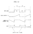
For example, as shown inFIG. 11A , if the gate of the Si-IGBT 110a of anupper arm 115a is turned on and the Si-IGBT 110b of alower arm 115b is turned off (shown by t1 inFIG. 12 ), a current Id flows from themidpoint 116 of thearm 113 to the load. After this current Id is applied to the load, the current is returned to a terminal on the low potential side of the direct-current power source via another arm (not shown) or the like. Thereafter, as shown inFIG. 11B , if the gate of the Si-IGBT 110a of theupper arm 115a is turned off (shown by t2 inFIG. 12 ), the commutation current Ifwd flows toward the load via the commutation diode (FWD) 114b of thelower arm 115b. At this time, when the gate of the Si-IGBT 110a is turned off, there is a problem in that the loss of the commutation current Ifwd that flows through thecommutation diode 114b becomes relatively large.
In addition, although a case where the Si-IGBT 110a of the above-describedupper arm 115a is turned off is described as an example, loss increases similarly even in a case where the commutation current flows to thecommutation diode 114a of theupper arm 115a when the Si-IGBT 110b of thelower arm 115b is turned off from ON. The loss mainly results from the voltage drop of thecommutation diodes - Thus, an object of the invention is to provide a switching circuit capable of reducing loss.
- In order to achieve the above object, the invention has adopted the following.
- (1) One aspect of the invention is a switching circuit including a
U-phase arm 13u, a V-phase arm 13v, or a W-phase arm 13w having two switching elements connected in series and reverse conducting elements connected in parallel to the switching elements, respectively. The switching elements are SiC semiconductors, and when a commutation current flows to the reverse conducting element, the switching element having the reverse conducting element connected in parallel thereto is turned on. - (2) The switching circuit described in (1) above may further include current-detecting means that detects the value of a current applied to the switching element, and on the basis of the value of a current applied to one switching element of the arm that is detected by the current-detecting means, the time for which the other switching element is turned on may be changed.
- (3) The switching circuit described in (2) above may further include temperature-detecting means that detects the temperature of the switching element, and when a commutation current flows to the reverse conducting element, the time for which the switching element may be turned on is changed on the basis of the detection result of the temperature-detecting means.
- According to the aspect described in (1) above, when a commutation current flows to the reverse conducting element, the switching element including a SiC semiconductor, having the reverse conducting element connected in parallel thereto, is turned on, whereby the commutation current that has being flowing to the reverse conducting element flows via the switching element that is an SiC semiconductor that has less loss and is more resistant to thermal destruction. Therefore, the loss when a current is commutated can be reduced.
- According to the aspect described in (2) above, in addition to the effects of the above (1), a commutation current according to the value of a current applied to one switching element flows. Thus, the time for which the other switching element when a current is commutated is turned on is changed according to the current value detected by the current-detecting means. Therefore, for example in a case where the current value detected by the temperature-detecting means is large, maximum loss reduction can be achieved while alleviating a burden caused by the heat generation of the other switching element, for example, by shortening the current-applied time of the other switching element by the ON operation.
- According to the aspect described in (2) above, in addition to the effects of the above (1), the time for which the switching element is turned on can be changed according to the temperature of the switching element detected by the temperature-detecting means. Therefore, for example, in a case where the temperature of the switching element is high, maximum loss reduction can be achieved by optimizing the ON time of the switching element when a current is commutated, while alleviating a burden caused by the heat generation of the switching element, for example, by shortening the current-applied time of the switching element by the ON operation.
-
-
FIG. 1 is a perspective view showing the layout of a hybrid vehicle in a first embodiment of the invention. -
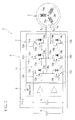
FIG. 2 is a circuit diagram of a system circuit that drives a motor in the first embodiment of the invention. -
FIG. 3 is a view showing one arm of the system circuit in the first embodiment of the invention. -
FIG. 4A shows a state where a drain current Id1 of afirst switching element 10a flows in the arm operation of the first embodiment of the invention. -
FIG. 4B shows a state where a commutation current flows to asecond diode 14b in the arm operation of the first embodiment of the invention. -
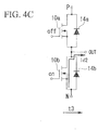
FIG. 4C shows a state where a drain current Id2 of asecond switching element 10b flows in the arm operation of the first embodiment of the invention. -
FIG. 5 is a timing chart showing the operation of the switching elements, the applied currents of the respective elements, and the magnitude of losses in the first embodiment of the invention. -
FIG. 6 is a graph showing changes in an applied current with respect to voltages between the terminals of the diodes and the switching elements in the first embodiment of the invention. -
FIG. 7A shows a state where the drain current Id1 of thefirst switching element 10a flows in the arm operation of a second embodiment of the invention. -
FIG. 7B shows a state where a commutation current flows to thesecond diode 14b in the arm operation of the second embodiment of the invention. -
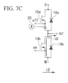
FIG. 7C shows a state where the drain current Id2 of thesecond switching element 10b flows in the arm operation of the second embodiment of the invention. -
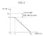
FIG. 8 is a graph showing the ON time of the second switching element to the applied current of the first switching element in the second embodiment of the invention. -
FIG. 9A shows a state where the drain current Id1 of thefirst switching element 10a flows in the arm operation of a third embodiment of the invention. -
FIG. 9B shows a state where a commutation current Ifwd flows to thesecond diode 14b in the arm operation of the third embodiment of the invention. -
FIG. 9C shows a state where the drain current Id2 of thesecond switching element 10b flows in the arm operation of the third embodiment of the invention. -
FIG. 10 is a graph showing the ON time of the second switching element to the temperature of the second switching element in the third embodiment of the invention. -
FIG. 11A shows a case where a current flows to an Si-IGBT of an upper arm in a switching circuit of the related art. -
FIG. 11 B shows a case where a commutation current Ifwd flows to a commutation diode of a lower arm in a switching circuit of the related art. -
FIG. 12 is a timing chart showing the operation of switching elements and the respective elements in the related art. - Respective embodiments of the invention will be described below with reference to the accompanying drawings.
FIG. 1 shows a hybrid vehicle 1 equipped with a switching circuit S of this embodiment. The hybrid vehicle 1 includes aninternal combustion engine 2, amotor 3, and a transmission (not shown). The hybrid vehicle 1 is a parallel type hybrid vehicle in which theinternal combustion engine 2, themotor 3, and the transmission (not shown) are directly connected together in series. The driving forces of both theinternal combustion engine 2 and themotor 3 are distributed and transmitted to left and right driving wheels W and W via the transmission and a differential (not shown). If a driving force is transmitted from the driving-wheel W side to themotor 3 side when the speed of the hybrid vehicle 1 is reduced, themotor 3 functions as a generator. That is, themotor 3 generates a so-called regenerative braking force when the speed of the hybrid vehicle 1 is reduced, and converts this force into electrical energy (electric power). This enables the kinetic energy of a vehicle body to be recovered as electrical energy. Moreover, themotor 3 is driven as a generator to generate power generation energy, depending on the output of theinternal combustion engine 2 according to the operational status of the hybrid vehicle 1. - As shown in
FIG. 2 , themotor 3 is, for example, a three-phase (U phase, V phase, and W phase) DC brushless motor or the like and is connected to a power control unit (PCU) 4 that controls the driving and power generation of themotor 3 viaharness power control unit 4 and a high-voltage battery 9 are arranged in the vicinity of a backseat of the hybrid vehicle 1. - The
power control unit 4 includes a smoothingcondenser 6, a power-driving unit (PDU) 7, and agate drive circuit 8 that controls the power-drivingunit 7. The high-voltage battery 9, which performs transfer of electric power (for example, supply power supplied to themotor 3 during driving or assist operation of themotor 3 or output power output from themotor 3 during power generation of themotor 3 by regeneration operation or boosting driving) with themotor 3 is connected to thepower control unit 4. The power-drivingunit 7 includes aPWM inverter 11. ThePWM inverter 11 includes a bridge circuit that performs bridge connection using a plurality of switchingelements PWM inverter 11 realizes an inverter operation using the pulse width modulation (PWM) of the bridge circuit. - The
PWM inverter 11 includes aU-phase arm 13u, a V-phase arm 13v, and a W-phase arm 13w. TheU-phase arm 13u, the V-phase arm 13v, and the W-phase arm 13w are configured by connecting in series anupper arm 15a including afirst switching element 10a that is a switching element and afirst diode 14a reverse-connected in parallel to thefirst switching element 10a, and alower arm 15b including asecond switching element 10b and asecond diode 14b reverse-connected in parallel to thesecond switching element 10b. Thefirst switching element 10a and thesecond switching element 10b include SiC semiconductors. Thefirst diode 14a and thesecond diode 14b include Si semiconductors. - The
U-phase coil 18u of themotor 3 is connected to amidpoint 16u where theupper arm 15a and thelower arm 15b of theU-phase arm 13u are connected, a V-phase coil 18v of themotor 3 is connected to amidpoint 16v where theupper arm 15a and thelower arm 15b of the V-phase arm 13v are connected, and a W-phase coil 18w of themotor 3 is connected to amidpoint 16w where theupper arm 15a and thelower arm 15b of the W-phase arm 13w are connected. AlthoughFIG. 2 shows an example of the arm in which MOSFETs are used as the switching elements, an arm using IGBT (Insulated Gate Bipolar Transistors) shown inFIG. 3 as theswitching elements FIG. 3 means a current that flows from + side of the high-voltage battery 9, and "N" means a current that flows to - side. - The power-driving
unit 7 receives a gate control signal by the pulse width modulation from thegate drive circuit 8 to control driving and power generation of themotor 3. For example, when themotor 3 is driven, direct-current power output from the high-voltage battery 9 is converted into 3-phase alternating-current power and is supplied to themotor 3, on the basis of a torque command output as a gate control signal from thegate drive circuit 8. On the other hand, during power generation of themotor 3, 3-phase alternating-current power output from themotor 3 is converted into direct-current power so as to charge the high-voltage battery 9. - The power conversion operation of the power-driving
unit 7 is controlled according to gate control signals input to gates G of thefirst switching element 10a and thesecond switching element 10b, which constitute the bridge circuit of thePWM inverter 11, from thegate drive circuit 8, that is, according to pulses for performing ON/OFF driving of thefirst switching element 10a and thesecond switching element 10b by the pulse width modulation (PWM). A map (data) of the duty of the pulses, that is, the ratio of ON/OFF, is stored in advance in thegate drive circuit 8. Here, the switching frequency obtained by the above-described PWM is a frequency exceeding 10 kHz. In addition, a current supplied to themotor 3 is detected by a current sensor that is not shown, and the measurement value of this motor current is fed back to thegate drive circuit 8. - Next, the power conversion operation using the power-driving
unit 7 described above will be described referring toFIGS. 4A to 4C andFIG. 5 . In addition, although this power conversion operation is performed at different timings, since the same control is performed in the respective arms of theU-phase arm 13u, the V-phase arm 13v, and the W-phase arm 13w, the operation of one arm will be described as an example and descriptions of the operation of the other two arms will be omitted. Additionally, for convenience, a current that flows when thefirst switching element 10a is in an ON state is referred to as a "first drain current Id1", and a current that flows when thesecond switching element 10b is in an ON state is referred to as a "second drain current Id2". -
FIG. 5 is a timing chart showing the operation of the switching elements, the applied currents of the respective elements, and the magnitude of loss in the first embodiment of the invention. The time of ON/OFF of the first switching element, the time for which the first drain current flows, the time of ON/OFF of the second switching element, the time for which the second drain current flows, and the time for which a commutation current Ifwd flows, and the loss in each time is shown byFIG. 5 . In time t1, the gate of thefirst switching element 10a of theupper arm 15a is in an ON state, and the gate of thesecond switching element 10b is in an OFF state. The drain current Id1 flows toward the motor 3 (in a direction indicated by an arrow inFIG. 4A ). In this case, the gate of thesecond switching element 10b of thelower arm 15b is turned off, and a current does not flow to thesecond switching element 10b of thelower arm 15b. The loss in this time t1 is the loss of thefirst switching element 10a that is mainly an SiC semiconductor. - Next, if time t2 comes, the gate of the
first switching element 10a of the upper arm is turned off, and the commutation current Ifwd (current in a direction indicated by an arrow inFIG. 4B ) that flows to themotor 3 via thesecond diode 14b of thelower arm 15b. The loss in time t2 is the loss of thesecond diode 14b. The loss caused by thesecond diode 14b becomes greater than the loss of the above-describedfirst switching element 10a. In addition, inFIG. 5 , at the moment when the gate G of thefirst switching element 10a or the gate G of thesecond switching element 10b is turned off from ON or turned on from OFF, loss increases temporarily because a large current flows temporarily due to inrush or the like to thesecond diode 14b. - Then, if time t3 comes, the gate of the
second switching element 10b of thelower arm 15b is turned on, the commutation current Ifwd that has flowed to thesecond diode 14b flows through thesecond switching element 10b, which is a SiC semiconductor, as the second drain current Id2 (current in a direction indicated by an arrow inFIG. 4C ). In this case, the loss of thesecond switching element 10b, which is a SiC semiconductor, becomes smaller than the loss of thesecond diode 14b in the time t2. Here, as shown inFIG. 5 , loss increases to an upward rise gradually and upwardly to the right from the flow start of the second drain current Id2, with the temperature rise of a switching element caused by current application. Additionally, time t2 and time t4 are so-called dead times provided so that thefirst switching element 10a and thesecond switching element 10b are not simultaneously turned on. - Moreover, if time t4 comes, the gate G of the
second switching element 10b is turned off, and the commutation current Ifwd flows again to thesecond diode 14b. Thereafter, the time t1 comes again, the gate of thefirst switching element 10a is turned on, and the same operation as the above-described operation is repeated. -
FIG. 6 is a graph in which the vertical axis shows a voltage (Vds) between terminals of the diodes including Si semiconductors and a voltage (Vf) between terminals of the switching elements including SiC semiconductors and the horizontal axis shows currents applied to the diodes and the switching elements including SiC semiconductors. As shown inFIG. 6 , the voltage (Vf) between the terminals of the switching elements including SiC semiconductors changes substantially linearly with respect to a current to be applied, whereas the voltage (Vds) between the terminals of the diodes shows a slightly nonlinear shape in which the increasing rate thereof become less as an applied current increases. - In
FIG. 6 , the voltage between the terminals of the switching elements and the voltage between the terminals of the diodes becomes almost equal at a predetermined current value shown by a broken line. In a region larger than the predetermined current value, the voltage Vf between the terminals of the switching elements becomes higher than the voltage (Vds) between the terminals of the diodes. Moreover, in a region smaller than the predetermined current value, the voltage (Vds) between the terminals of the diodes becomes higher than the switching elements (Vf). - That is, in the time t3 of
FIG. 5 , the value of the second drain current Id2 of thesecond switching element 10b is in a current region that is less than the predetermined current value of the graph ofFIG. 6 . That is, thesecond switching element 10b is turned on in a region where a voltage drop due to thesecond switching element 10b is smaller than a voltage drop due to thesecond diode 14b. - Accordingly, according to the first embodiment, when the commutation current Ifwd flows to the
second diode 14b (reverse conducting element), thesecond switching element 10b including a SiC semiconductor, which is connected in parallel to thesecond diode 14b, is turned on, whereby the commutation current Ifwd that has been flowing to thesecond diode 14b (reverse conducting element) flows as the second drain current Id2 via thesecond switching element 10b that is an SiC semiconductor that has less loss and is more resistant to thermal destruction. For this reason, it is possible to reduce the loss when a current is commutated. - In addition, although a case where the commutation current Ifwd of the
second diode 14b that flows when thefirst switching element 10a is switched from ON to OFF is applied as the second drain current Id2 of thesecond switching element 10b has been described as an example in the first embodiment, the commutation current Ifwd that flows to thefirst diode 14a (reverse conducting element) when thesecond switching element 10b is controlled from ON to OFF may be applied as the first drain current Id1 of thefirst switching element 10a. That is, thefirst switching element 10a including an SiC semiconductor that is connected in parallel to thefirst diode 14a (reverse conducting element) is turned on, whereby the commutation current Ifwd that has been flowing to thefirst diode 14a flows as the first drain current Id1 via thefirst switching element 10a that is an SiC semiconductor that has less loss and is more resistant to thermal destruction. - Next, a switching circuit S in the second embodiment of the invention will be described, incorporating
FIG. 2 of the first embodiment and referring toFIGS. 7A to 7C . In addition, since the second embodiment is different from the first embodiment only in terms of control related to ON of the gate of thesecond switching element 10b, description will be made with the same portions being designated by the same reference numerals. In addition, even in the second embodiment, the same control is performed in the respective arms of theU-phase arm 13u, the V-phase arm 13v, and the W-phase arm 13w. Therefore, the operation of one arm will be described as an example and descriptions of the operation of the other two arms will be omitted. - The switching circuit S in the second embodiment is able to detect the first drain current Id1 that flows to the
first switching element 10a using a current sensor 20 (current-detecting means: refer toFIGS. 7A to 7C ), and change the ON time of thesecond switching element 10b when the commutation current Ifwd flows to thesecond diode 14b, according to the magnitude of the detected first drain current Id1. That is, the length of the time t3 can be controlled. -
FIG. 8 shows the relationship between the ON time t3 of thesecond switching element 10b and the first drain current Id1 that flows to thefirst switching element 10a. The vertical axis shows the ON time of thesecond switching element 10b, and the horizontal axis shows the first drain current Id1 that flows to thefirst switching element 10a. The ON time of thesecond switching element 10b corresponds to t3 inFIG. 5 . As shown in the graph ofFIG. 8 , the ON time t3 of thesecond switching element 10b is a constant time to until the first drain current Id1 reaches a predetermined current value Id1=I0 from "0". In a case where the first drain current Id1 exceeds the predetermined current value I0, the ON time t3 of thesecond switching element 10b is shortened at a predetermined inclination with an increase in the first drain current Id1. In a case where the first drain current Id1 reaches a predetermined upper limit IMAX, the ON time t3 of thesecond switching element 10b is "0". Here, the portion where the constant ON time t3=t0 is established is set in order to provide the above-described dead times, and the ON time t3 is made not to extend any more. InFIG. 8 , an upper broken line is the longest time (tMAX) of the sum (t2+t3+t4) of the time t2, the time t3, and the time t4, and a broken line therebelow is ON time t3=t0 that is a predetermined constant value. The time between these broken lines is secured as the minimum value (t2+t4) MIN of the above-described dead times. - Accordingly, according to the second embodiment, the commutation current Ifwd according to the current value of the first drain current Id1 of the
first switching element 10a flows when thefirst switching element 10a is turned off. Thus, maximum loss reduction can be achieved while reducing heat generation of thesecond switching element 10b by current application to alleviate a burden on thesecond switching element 10b, by shortening the time t3, during which thesecond switching element 10b when a current is commutated is turned on, as the current value of the first drain current Id1 of thefirst switching element 10a increases.
In addition, although a case where the commutation current Ifwd of thesecond diode 14b that flows when thefirst switching element 10a is switched from ON to OFF is applied as the second drain current Id2 of thesecond switching element 10b has been described as an example in the second embodiment, the commutation current Ifwd that flows to thefirst diode 14a when thesecond switching element 10b is controlled from ON to OFF may be applied as the first drain current Id1 of thefirst switching element 10a. - Next, a switching circuit S in the third embodiment of the invention will be described, incorporating
FIG. 2 of the above-described first embodiment and referring toFIGS. 9A to 9C . In addition, since the third embodiment is different from the above-described second embodiment only in terms of control related to ON of the gate of thesecond switching element 10b, description will be made with the same portions being designated by the same reference numerals. Even in the third embodiment, the same control is performed in the respective arms of theU-phase arm 13u, the V-phase arm 13v, and the W-phase arm 13w. Therefore, the operation of one arm will be described as an example and descriptions of the operation of the other two arms will be omitted. - A switching circuit S in a third embodiment is able to detect the temperature of the
second switching element 10b using a temperature sensor 30 (temperature-detecting means: refer toFIGS. 9A to 9C ), and change the ON time of thesecond switching element 10b when the commutation current Ifwd flows to thesecond diode 14b according to this detected temperature. That is, the length of the time t3 can be controlled. -
FIG. 10 is a graph in which the vertical axis shows the ON time t3 of thesecond switching element 10b and the horizontal axis shows the temperature T of thesecond switching element 10b (FET temperature). As shown in this graph, if the temperature of thesecond switching element 10b is lower than or equal to a predetermined temperature, the ON time t3 of thesecond switching element 10b is a predetermined constant time t0. In a case where the temperature of thesecond switching element 10b exceeds the predetermined temperature To, the ON time t3 of thesecond switching element 10b is shortened at a predetermined inclination according to the temperature rise of thesecond switching element 10b. In a case where the temperature of thesecond switching element 10b reaches a predetermined upper limit TMAX, the ON time t3 of thesecond switching element 10b is "0". InFIG. 10 , an upper broken line is the sum (t2+t3+t4)MAX of the time t2, the time t3, and the time t4, and a broken line therebelow is ON time t3=t0 that is a constant value. The time between these broken lines is secured as the minimum value (t2+t4) MIN of the above-described dead times. - Accordingly, according to the above-mentioned third embodiment, the time for which the
second switching element 10b is turned on can be changed according to the temperature of thesecond switching element 10b detected by thetemperature sensor 30. Therefore, in a case where the temperature of thesecond switching element 10b is high, maximum loss reduction can be achieved while alleviating a burden caused by the heat generation of thesecond switching element 10b by shortening the current-applied time of thesecond switching element 10b by the ON operation.
In addition, although a case where the commutation current Ifwd of thesecond diode 14b that flows when thefirst switching element 10a is switched from ON to OFF is applied as the second drain current Id2 of thesecond switching element 10b has been described as an example in the third embodiment, the commutation current Ifwd that flows to thefirst diode 14a when thesecond switching element 10b is controlled from ON to OFF may be applied as the first drain current Id1 of thefirst switching element 10a. - In addition, the invention is not limited to the above-described respective embodiments. For example, the
first diode 14a and thesecond diode 14b for commutation can be changed to Schottky barrier diodes including SiC semiconductors with less loss than the diodes including Si semiconductors. In this case, the above-described losses in the times t2 and t4 can be reduced. However, as conditions in which the invention is applied, a case is preferable where the losses of the Schottky barrier diodes including SiC semiconductors become larger than losses of the switching elements including SiC semiconductors, that is, the loss of thefirst switching element 10a and the loss of thesecond switching element 10b.
Additionally, in the above-described respective embodiments, a case where the commutation current Ifwd that flows to thesecond diode 14b after thefirst switching element 10a is turned off is applied via thesecond switching element 10b. However, the commutation current Ifwd that flows to thefirst diode 14a after thesecond switching element 10b is turned off may be applied viafirst switching element 10a. - Additionally, in the second embodiment, a case where the
first switching element 10a is provided with thecurrent sensor 20 and the time t3 during which thesecond switching element 10b is turned on is changed on the basis of the detection result of thecurrent sensor 20 has been described. However, a current sensor (not shown) that detects the current (ILoad) that flows to the motor from the midpoint 16 may be provided, and the time t3 may be changed on the basis of the detection result of this current sensor. - A switching circuit capable of reducing loss can be provided.
-
- 10a:
- FIRST SWITCHING ELEMENT (SWITCHING ELEMENT)
- 10b:
- SECOND SWITCHING ELEMENT (SWITCHING ELEMENT)
- 14a:
- FIRST DIODE (REVERSE CONDUCTING ELEMENT)
- 14b:
- SECOND DIODE (REVERSE CONDUCTING ELEMENT)
- 13u:
- U-PHASE ARM
- 13v:
- V-PHASE ARM
- 13w:
- W-PHASE ARM
- 20:
- CURRENT SENSOR (CURRENT-DETECTING MEANS)
- 30:
- TEMPERATURE SENSOR (TEMPERATURE-DETECTING MEANS)
Claims (3)
- A switching circuit comprising an arm having two switching elements connected in series and reverse conducting elements connected in parallel to the switching elements,
wherein the switching elements are SiC semiconductors, and
when a commutation current flows to the reverse conducting element, the switching element having the reverse conducting element connected in parallel thereto is turned on. - The switching circuit according to Claim 1, further comprising:a commutation current-detecting unit that detects the current value of the commutation current,wherein when a commutation current flows to the reverse conducting element, the time for which the switching element is turned on is changed on the basis of the detection result of the commutation current-detecting unit.
- The switching circuit according to Claim 1, further comprising:a temperature-detecting unit that detects the temperature of the switching element,wherein when a commutation current flows to the reverse conducting element, the time for which the switching element is turned on is changed on the basis of the detection result of the temperature-detecting unit.
Applications Claiming Priority (2)
| Application Number | Priority Date | Filing Date | Title |
|---|---|---|---|
| JP2010103840 | 2010-04-28 | ||
| PCT/JP2011/058913 WO2011136003A1 (en) | 2010-04-28 | 2011-04-08 | Switching circuit |
Publications (2)
| Publication Number | Publication Date |
|---|---|
| EP2566034A1 true EP2566034A1 (en) | 2013-03-06 |
| EP2566034A4 EP2566034A4 (en) | 2014-12-24 |
Family
ID=44861315
Family Applications (1)
| Application Number | Title | Priority Date | Filing Date |
|---|---|---|---|
| EP11774787.3A Withdrawn EP2566034A4 (en) | 2010-04-28 | 2011-04-08 | Switching circuit |
Country Status (5)
| Country | Link |
|---|---|
| US (1) | US20130038140A1 (en) |
| EP (1) | EP2566034A4 (en) |
| JP (1) | JP5592943B2 (en) |
| CN (1) | CN102859859A (en) |
| WO (1) | WO2011136003A1 (en) |
Cited By (2)
| Publication number | Priority date | Publication date | Assignee | Title |
|---|---|---|---|---|
| EP3306801A4 (en) * | 2015-06-02 | 2019-01-02 | Hitachi Industrial Equipment Systems Co., Ltd. | Power conversion device and motor device |
| EP3518422A1 (en) * | 2018-01-26 | 2019-07-31 | General Electric Company | Switch controller for adaptive reverse conduction control in switch devices |
Families Citing this family (15)
| Publication number | Priority date | Publication date | Assignee | Title |
|---|---|---|---|---|
| JP5485232B2 (en) | 2011-07-04 | 2014-05-07 | 本田技研工業株式会社 | Switching circuit control device |
| JP5822773B2 (en) * | 2012-04-17 | 2015-11-24 | 三菱電機株式会社 | Power converter |
| CN103855913A (en) * | 2012-11-30 | 2014-06-11 | 通用电气公司 | Energy transformation system and control method |
| CN103944426B (en) * | 2014-05-05 | 2017-08-08 | 广州金升阳科技有限公司 | A kind of synchronous rectification implementation method |
| EP3026801B1 (en) * | 2014-11-26 | 2021-03-10 | Mitsubishi Electric R&D Centre Europe B.V. | Device for controlling the operation of a multi-die power module |
| JP2017077096A (en) * | 2015-10-15 | 2017-04-20 | 富士電機株式会社 | Power converter |
| JP6747046B2 (en) * | 2016-05-12 | 2020-08-26 | 富士電機株式会社 | Boost chopper circuit |
| JP6701520B2 (en) * | 2016-05-13 | 2020-05-27 | 富士電機株式会社 | Power converter |
| US10020723B1 (en) | 2016-06-25 | 2018-07-10 | Active-Semi, Inc. | Power loss protection integrated circuit with autonomous capacitor health check |
| US10985644B1 (en) | 2016-06-25 | 2021-04-20 | Active-Semi, Inc. | Optimized gate driver for low voltage power loss protection system |
| US10090675B1 (en) | 2016-06-25 | 2018-10-02 | Active-Semi, Inc. | Fast settlement of supplement converter for power loss protection system |
| US10826480B1 (en) * | 2016-07-01 | 2020-11-03 | Active-Semi, Inc. | Gate driver to decrease EMI with shorter dead-time |
| CN107393737A (en) * | 2017-09-11 | 2017-11-24 | 广东电网有限责任公司电力科学研究院 | A kind of primary cut-out electric operating mechanism containing energy storage device |
| CN112542949A (en) * | 2019-09-23 | 2021-03-23 | 中车株洲电力机车研究所有限公司 | Control method and device of DC-DC circuit |
| CN113131833B (en) | 2019-12-31 | 2023-03-14 | 比亚迪股份有限公司 | Motor control system and motor control device |
Family Cites Families (13)
| Publication number | Priority date | Publication date | Assignee | Title |
|---|---|---|---|---|
| JP2812528B2 (en) * | 1990-03-20 | 1998-10-22 | 株式会社日立製作所 | Inverter circuit |
| US7088565B2 (en) * | 2002-04-12 | 2006-08-08 | Denso Corporation | Load drive control apparatus with performances of power-consumption reduction and overheat protection |
| JP4306236B2 (en) | 2002-12-05 | 2009-07-29 | 株式会社豊田中央研究所 | DC voltage converter |
| US7492138B2 (en) * | 2004-04-06 | 2009-02-17 | International Rectifier Corporation | Synchronous rectifier circuits and method for utilizing common source inductance of the synchronous FET |
| JP4204534B2 (en) * | 2004-11-15 | 2009-01-07 | 株式会社東芝 | Power converter |
| JP2007014059A (en) * | 2005-06-28 | 2007-01-18 | Toyota Motor Corp | Switching circuit |
| JP5230068B2 (en) * | 2006-01-13 | 2013-07-10 | オムロンオートモーティブエレクトロニクス株式会社 | Inverter device |
| US7782005B2 (en) * | 2006-11-07 | 2010-08-24 | Nissan Motor Co., Ltd. | Power converter control |
| JP5104083B2 (en) * | 2006-11-07 | 2012-12-19 | 日産自動車株式会社 | Power conversion device and power conversion method |
| WO2009081561A1 (en) * | 2007-12-20 | 2009-07-02 | Panasonic Corporation | Power conversion device, switch device and method for controlling power conversion device |
| JP5770412B2 (en) * | 2008-01-31 | 2015-08-26 | ダイキン工業株式会社 | Power converter |
| JP4536128B2 (en) * | 2008-05-19 | 2010-09-01 | 本田技研工業株式会社 | DC / DC converter device, fuel cell vehicle equipped with the DC / DC converter device, and DC / DC converter control method |
| JP4906890B2 (en) * | 2009-06-02 | 2012-03-28 | 三菱電機株式会社 | Bridge rectifier circuit |
-
2011
- 2011-04-08 CN CN2011800206210A patent/CN102859859A/en active Pending
- 2011-04-08 JP JP2012512752A patent/JP5592943B2/en not_active Expired - Fee Related
- 2011-04-08 EP EP11774787.3A patent/EP2566034A4/en not_active Withdrawn
- 2011-04-08 US US13/643,853 patent/US20130038140A1/en not_active Abandoned
- 2011-04-08 WO PCT/JP2011/058913 patent/WO2011136003A1/en not_active Ceased
Cited By (2)
| Publication number | Priority date | Publication date | Assignee | Title |
|---|---|---|---|---|
| EP3306801A4 (en) * | 2015-06-02 | 2019-01-02 | Hitachi Industrial Equipment Systems Co., Ltd. | Power conversion device and motor device |
| EP3518422A1 (en) * | 2018-01-26 | 2019-07-31 | General Electric Company | Switch controller for adaptive reverse conduction control in switch devices |
Also Published As
| Publication number | Publication date |
|---|---|
| US20130038140A1 (en) | 2013-02-14 |
| CN102859859A (en) | 2013-01-02 |
| JP5592943B2 (en) | 2014-09-17 |
| JPWO2011136003A1 (en) | 2013-07-18 |
| EP2566034A4 (en) | 2014-12-24 |
| WO2011136003A1 (en) | 2011-11-03 |
Similar Documents
| Publication | Publication Date | Title |
|---|---|---|
| EP2566034A1 (en) | Switching circuit | |
| US10491095B2 (en) | Dynamic IGBT gate drive for vehicle traction inverters | |
| US10291168B2 (en) | Power conversion control apparatus | |
| CN106104998B (en) | Control device for inverter | |
| US10071652B2 (en) | Dual mode IGBT gate drive to reduce switching loss | |
| US10090792B2 (en) | Self-balancing parallel power devices with a temperature compensated gate driver | |
| CN107148738B (en) | power conversion device | |
| US10211827B2 (en) | Resonant gate driver | |
| JP7279329B2 (en) | Charge control method and charge control device | |
| US9837887B1 (en) | IGBT gate drive with active turnoff to reduce switching loss | |
| US9281776B2 (en) | Power conversion apparatus including different voltage-type bridge circuits | |
| US20170222641A1 (en) | Dynamic igbt gate drive to reduce switching loss | |
| US10144296B2 (en) | Gate driver with temperature compensated turn-off | |
| CN103872970B (en) | For operating circuit arrangement and the method for motor | |
| JP6218906B1 (en) | Power converter | |
| US11728802B2 (en) | Drive circuit | |
| CN111231692A (en) | Inverter system with enhanced common source inductance generated at gate driver | |
| CN103813929B (en) | There is the drive system of the battery operation vehicle of the permanent excited synchronous motor of being powered by current converter | |
| JP6165216B2 (en) | Method for manufacturing motor drive device | |
| JP2020058177A (en) | Charge control method and charge control device | |
| US10848049B2 (en) | Main conversion circuit, power conversion device, and moving body | |
| US20250274056A1 (en) | Method of operating an inverter circuit, inverter arrangement and drive unit | |
| JP7421435B2 (en) | Motor control device and motor control method | |
| JP6896042B2 (en) | Power conversion circuit | |
| CN117526778A (en) | Method and device for operating at least one switching device of a rectifier of a trolley drive of a motor vehicle |
Legal Events
| Date | Code | Title | Description |
|---|---|---|---|
| PUAI | Public reference made under article 153(3) epc to a published international application that has entered the european phase |
Free format text: ORIGINAL CODE: 0009012 |
|
| 17P | Request for examination filed |
Effective date: 20121107 |
|
| AK | Designated contracting states |
Kind code of ref document: A1 Designated state(s): AL AT BE BG CH CY CZ DE DK EE ES FI FR GB GR HR HU IE IS IT LI LT LU LV MC MK MT NL NO PL PT RO RS SE SI SK SM TR |
|
| DAX | Request for extension of the european patent (deleted) | ||
| A4 | Supplementary search report drawn up and despatched |
Effective date: 20141126 |
|
| RIC1 | Information provided on ipc code assigned before grant |
Ipc: H03K 17/14 20060101ALI20141120BHEP Ipc: H03K 17/08 20060101ALI20141120BHEP Ipc: H03K 17/74 20060101ALN20141120BHEP Ipc: H02M 7/5387 20070101AFI20141120BHEP Ipc: H03K 17/0814 20060101ALN20141120BHEP Ipc: H02P 27/08 20060101ALI20141120BHEP |
|
| 17Q | First examination report despatched |
Effective date: 20141209 |
|
| STAA | Information on the status of an ep patent application or granted ep patent |
Free format text: STATUS: THE APPLICATION IS DEEMED TO BE WITHDRAWN |
|
| 18D | Application deemed to be withdrawn |
Effective date: 20170125 |