EP2566023B1 - Line filter for a switching power supply - Google Patents
Line filter for a switching power supply Download PDFInfo
- Publication number
- EP2566023B1 EP2566023B1 EP12180593.1A EP12180593A EP2566023B1 EP 2566023 B1 EP2566023 B1 EP 2566023B1 EP 12180593 A EP12180593 A EP 12180593A EP 2566023 B1 EP2566023 B1 EP 2566023B1
- Authority
- EP
- European Patent Office
- Prior art keywords
- power supply
- transformer
- line filter
- capacitor
- line
- Prior art date
- Legal status (The legal status is an assumption and is not a legal conclusion. Google has not performed a legal analysis and makes no representation as to the accuracy of the status listed.)
- Active
Links
Images


Classifications
-
- H—ELECTRICITY
- H02—GENERATION; CONVERSION OR DISTRIBUTION OF ELECTRIC POWER
- H02M—APPARATUS FOR CONVERSION BETWEEN AC AND AC, BETWEEN AC AND DC, OR BETWEEN DC AND DC, AND FOR USE WITH MAINS OR SIMILAR POWER SUPPLY SYSTEMS; CONVERSION OF DC OR AC INPUT POWER INTO SURGE OUTPUT POWER; CONTROL OR REGULATION THEREOF
- H02M1/00—Details of apparatus for conversion
- H02M1/12—Arrangements for reducing harmonics from ac input or output
- H02M1/126—Arrangements for reducing harmonics from ac input or output using passive filters
-
- H—ELECTRICITY
- H02—GENERATION; CONVERSION OR DISTRIBUTION OF ELECTRIC POWER
- H02M—APPARATUS FOR CONVERSION BETWEEN AC AND AC, BETWEEN AC AND DC, OR BETWEEN DC AND DC, AND FOR USE WITH MAINS OR SIMILAR POWER SUPPLY SYSTEMS; CONVERSION OF DC OR AC INPUT POWER INTO SURGE OUTPUT POWER; CONTROL OR REGULATION THEREOF
- H02M1/00—Details of apparatus for conversion
- H02M1/12—Arrangements for reducing harmonics from ac input or output
-
- G—PHYSICS
- G03—PHOTOGRAPHY; CINEMATOGRAPHY; ANALOGOUS TECHNIQUES USING WAVES OTHER THAN OPTICAL WAVES; ELECTROGRAPHY; HOLOGRAPHY
- G03G—ELECTROGRAPHY; ELECTROPHOTOGRAPHY; MAGNETOGRAPHY
- G03G21/00—Arrangements not provided for by groups G03G13/00 - G03G19/00, e.g. cleaning, elimination of residual charge
-
- H—ELECTRICITY
- H02—GENERATION; CONVERSION OR DISTRIBUTION OF ELECTRIC POWER
- H02M—APPARATUS FOR CONVERSION BETWEEN AC AND AC, BETWEEN AC AND DC, OR BETWEEN DC AND DC, AND FOR USE WITH MAINS OR SIMILAR POWER SUPPLY SYSTEMS; CONVERSION OF DC OR AC INPUT POWER INTO SURGE OUTPUT POWER; CONTROL OR REGULATION THEREOF
- H02M3/00—Conversion of dc power input into dc power output
- H02M3/22—Conversion of dc power input into dc power output with intermediate conversion into ac
- H02M3/24—Conversion of dc power input into dc power output with intermediate conversion into ac by static converters
- H02M3/28—Conversion of dc power input into dc power output with intermediate conversion into ac by static converters using discharge tubes with control electrode or semiconductor devices with control electrode to produce the intermediate ac
-
- H—ELECTRICITY
- H02—GENERATION; CONVERSION OR DISTRIBUTION OF ELECTRIC POWER
- H02M—APPARATUS FOR CONVERSION BETWEEN AC AND AC, BETWEEN AC AND DC, OR BETWEEN DC AND DC, AND FOR USE WITH MAINS OR SIMILAR POWER SUPPLY SYSTEMS; CONVERSION OF DC OR AC INPUT POWER INTO SURGE OUTPUT POWER; CONTROL OR REGULATION THEREOF
- H02M1/00—Details of apparatus for conversion
- H02M1/12—Arrangements for reducing harmonics from ac input or output
- H02M1/123—Suppression of common mode voltage or current
Definitions
- the present invention relates to a line filter provided as a noise filter in a converter configured to rectify and convert an alternating-current (AC) voltage input from a commercial AC power supply.
- AC alternating-current
- a conventional line filter includes a first noise filter 25 between a power plug 1 plugged and unplugged to/from a commercial AC power supply and a rectifier unit 3 for rectifying an input AC voltage, a second noise filter 26 between the rectifier unit 3 and a transformer 7, and a resistor 31 between the power plug 1 and the rectifier unit 3 (as disclosed for example in the US patent application Nr. 4,667,173 ).
- the first noise filter 25 includes a first choke coil 27, a first X capacitor (across-the-line capacitor) 28, and first Y capacitors (line-bypass capacitors) 29 and 30 connected to the earth (also referred to as the ground) 2.
- the second noise filter 26 includes a second choke coil 32, a second X capacitor 33, and second Y capacitors 34 and 35 connected to the earth 2.
- the above-described conventional line filter has yet the following first problem since the influence of a radiation unit for radiating heat generated during operation of a switching unit 8 for driving the transformer 7 has not been taken into consideration.
- the switching unit 8 When the switching unit 8 operates, the switching unit 8 and the radiation unit are electrically coupled and a current flows through a stray capacitance between the radiation unit and the earth 2, resulting in common mode noise.
- the above-described conventional line filter has yet a second problem that the resistor 31 between the commercial AC power supply and the rectifier unit (also referred to as a rectification bridge) 3 consumes electric power that does not contribute to power supply.
- the resistor 31 is a discharge resistor for discharging the energy (charge) accumulated in the first X capacitor 28 connected between the output lines of the power plug 1 plugged and unplugged to/from the commercial AC power supply. Thus, when the power plug 1 is unplugged, the resistor 31 ensures user's safety even if the user touches a terminal of the power plug 1.
- An international safety standard prescribes that, if the capacitance of an electromagnetic interference (EMI) filter exceeds a threshold value (typically, 0.1 ⁇ F), the voltage between both input terminals of the power source shall be reduced to a safe level within a predetermined time period after the power plug is unplugged.
- EMI electromagnetic interference
- the document JP-H11 356047 discloses a common mode EMI filter for an isolated switching power supply, wherein noise currents flow through a heatsink on the primary side of the power supply.
- the present invention is directed to a line filter capable of sufficiently reducing noise in a configuration having a radiation unit for radiating heat generated during operation of a switching unit. Further, the present invention is directed to a line filter capable of reducing the power consumption related to a discharge resistor for discharging the charge accumulated in an X capacitor connected between output lines of a power plug.
- a line filter as specified in claims 1 to 6.
- a switching power supply as specified in claim 7.
- an image forming apparatus as specified in claim 8.
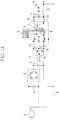
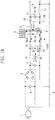
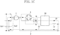
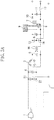
- Figs. 1A , 1B , and 1C each illustrate a configuration of a line filter according to a first exemplary embodiment.
- Figs. 1A and 1B illustrate a circuit of a switching power supply (also referred to as an AC/DC converter) .
- the circuit rectifies and smoothes an AC voltage input from a commercial AC power supply and supplies a resultant voltage to a transformer 7.
- a switching unit 8 drives the primary side of the transformer 7 to generate an AC voltage on the secondary side of the transformer 7. Then, the circuit rectifies and smoothes the resultant AC voltage to output a resultant DC voltage.
- a power plug 1 is plugged and unplugged to/from the commercial AC power supply.
- the earth 2 is connected to an earth terminal (also referred to as a ground terminal) of the power plug 1.
- a rectifier unit (also referred to as a rectification bridge) 3 rectifies an input AC voltage.
- a third capacitor 4 is connected between the lines at a position between the power plug 1 and the rectifier unit 3.
- a fourth capacitor 5 is connected between rectification output lines of the rectifier unit 3 at a position immediately after the rectifier unit 3.
- a first smoothing capacitor 6 smoothes the rectified voltage output from the rectifier unit 3.
- the transformer 7 transforms a voltage input via the first smoothing capacitor 6 and outputs a resultant voltage.
- the switching unit 8 is connected to the transformer 7.
- a radiation unit 9 radiates heat generated during operation of the switching unit 8.
- the switching unit 8 includes a field effect transistor (FET).
- FET field effect transistor
- the radiation unit 9 is provided with a radiation pattern.
- a rectifier diode 10 rectifies the output voltage of the transformer 7.
- a second smoothing capacitor 11 smoothes the output of the rectifier diode 10.
- a first current path 12 feeds a current flowing through the radiation unit 9 back to the switching unit 8.
- One end of a first capacitor 13 is connected to the positive electrode side of the line between the fourth capacitor 5 and the transformer 7.
- One end of a second capacitor 14 is connected to the negative electrode side of the line between the fourth capacitor 5 and the transformers 7.
- a second current path 15 feeds an output current of the transformer 7 back to the switching unit 8 via the first capacitor 13 and the second capacitor 14.
- a first coil 16 suppresses a common mode current 18 flowing between the third capacitor 4 and the first and second capacitors 13 and 14.
- a second coil 17 suppresses a common mode current 19 flowing between the transformer 7 and the output.
- first and second current paths two different current paths (first and second current paths) are provided, a configuration having either one of the current paths enables acquiring the effect of noise current reduction.
- a current Ihc0 flowing through the radiation unit 9 configured to radiate heat generated during operation of the switching unit 8 is fed back to the switching unit 8 via the first current path 12 separately provided from the earth 2 coupled with the stray capacitance.
- the current ItcO has been described to be fed back to the switching unit 8 via the first capacitor 13 and the second capacitor 14, even if either one of the capacitors 13 and 14 is provided, the current ItcO can be fed back to the switching unit 8 via the connection path of the capacitor.
- Suppressing the common mode current 18 via the first coil 16 enables preventing the common mode current 18 generated during the operation of the switching unit 8 from flowing to the side of the commercial AC power supply.
- Suppressing the common mode current 19 via the second coil 17 enables preventing the common mode current 19 generated during the operation of the switching unit 8 from flowing to the output side.
- Fig. 1C illustrates a simplified connection on the side of the commercial AC power supply illustrated in Fig. 1A .
- the components 6 to 15 in Fig. 1A are illustrated as a four-terminal network 36.
- a common mode current 37 flows between the earth 2 and the lines.
- Figs. 1A and 1B the common mode currents 18 and 19 are described to be different currents, both currents are actually identical to the common mode current 37. Therefore, in Fig. 1B , the configuration of the line filter has been described to include two coils (the first coil 16 and the second coil 17), a similar effect can be acquired with either one of the coils.
- a common mode choke coil is used as the first coil 16 and a normal coil as the second coil 17, the first and second coils 16 and 17 are not limited thereto as long as they can suppress the common mode current.
- the first capacitor 13 and the second capacitor 14 are provided between the first coil 16 and the first smoothing capacitor 6, the configuration is not limited thereto as long as they are provided between the first coil 16 and the transformer 7.
- a noise filter near the rectifier unit 3 will be described below with reference to Fig. 1A .
- the rectifier unit 3 is rectifying the AC voltage, specifically, during a time period when a forward current flows from the input side to the output side of the rectifier unit 3 the fourth capacitor 5 functions as a noise filter similar to the third capacitor 4.
- the third capacitor 4 functions as a noise filter.
- a reverse current flows from the output side to the input side of the rectifier unit 3 mainly because of a recovery current due to recovery characteristics of the rectifier unit 3 (recovery characteristics of a rectifier diode).
- the capacitance of the third capacitor 4 is set to bypass noise component contained in the reverse current, and the capacitance of the fourth capacitor 5 is set to provide a capacitance for filtering noise component contained in the forward current.
- the capacitance (including the third capacitor 4) between the lines at a position between the power plug 1 and the rectifier unit 3 is set to 0.1 ⁇ F or less based on the international safety standard. Therefore, it is not necessary to provide a discharge resistor for discharging the capacitance between the lines at a position between the power plug 1 and the rectifier unit 3. This enables reducing the power consumption that does not contribute to the power supply related to the capacitor connected between the output lines of the power plug 1.
- the capacitance of the first X capacitor 28 is 1.0 ⁇ F
- the capacitance of the third capacitor 4 is set to 0.1 ⁇ F and the capacitance of the fourth capacitor 5 to 0.9 ⁇ F.
- the capacitance of the third capacitor 4 can be set to 0.1 ⁇ F and the capacitance of the fourth capacitor 5 to 10.0 ⁇ F.
- the rectifier unit 3 separates the fourth capacitor 5 from the capacitor connected between the output lines of the power plug 1 when the power plug 1 is unplugged.
- the present exemplary embodiment enables suppressing noise due to the influence of a radiation unit configured to radiate heat generated during operation of the switching unit.
- the present exemplary embodiment further enables eliminating a discharge resistor as a discharge unit for discharging the charge accumulated in the X capacitor, resulting in reduced power consumption.
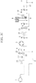
- FIG. 2 illustrates a line filter according to the second exemplary embodiment, having a modified configuration of the circuit according to the first exemplary embodiment. Differences of the line filter according to the second exemplary embodiment from the line filter according to the first exemplary embodiment will be described below.
- the line filter according to the second exemplary embodiment has a circuit configuration in which a common mode choke coil 20 for suppressing a common mode current is connected between the rectifier unit 3 and the fourth capacitor 5.
- This circuit configuration enables enhancing characteristics for suppressing a common mode current generated during operation of a switching unit 8. This enables configuring a noise filter optimized for a common mode current having a frequency to be suppressed.
- the present exemplary embodiment has been described to apply a common mode choke coil for suppressing a common mode current
- the coil configured to suppress a common mode current is not limited thereto.
- the common mode choke coil 20 is used as a coil for suppressing the common mode current, the common mode choke coil 20 has a coupling factor as close as possible to "1" (maximum value).
- the coupling factor is "0.99", for example, a value "20.01” functions also as a normal mode coil.
- a common mode choke coil configured to have a coupling factor smaller than "1" as the first common mode choke coil 20 and the first coil 16 enables the first common mode choke coil 20, the fourth capacitor 5, and the first coil 16 to function as a normal-mode T-type LC filter, without increasing the number of parts.
- a coupling factor for achieving both the normal-mode filter function and the common-mode filter function may be suitably set based on the current value to be suppressed.
- the present exemplary embodiment also enables suppressing noise due to the influence of the radiation unit configured to radiate heat generated during operation of the switching unit.
- the present exemplary embodiment further enables eliminating the discharge resistance of a radiation unit configured to discharge the charge accumulated in the X capacitor, resulting in reduced power consumption.
- the present exemplary embodiment further enhances a function of suppressing a common mode current to suppress common mode noise.
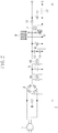
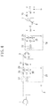
- FIG. 3A , 3B , and 3C each illustrate a line filter according to the third exemplary embodiment, having a modified configuration of the circuit according to the first exemplary embodiment.
- a fifth capacitor 21 and a sixth capacitor 22 are connected in series between the power plug 1 and the rectifier unit 3.
- a connecting portion of the fifth capacitor 21 and the sixth capacitor 22 is connected to the earth 2.
- This circuit configuration if the common mode current by the stray capacitance between the rectifier unit 3 and the earth 2 has a large influence, enables bypassing the common mode current to the earth 2 via the fifth capacitor 21 and the sixth capacitor 22. This prevents the common mode current from flowing to the side of the commercial AC power supply.
- a common mode choke coil 23 for suppressing a common mode current is connected between the power plug 1 and the fifth and sixth capacitors 21 and 22.
- This circuit configuration suppresses the common mode current via the second common mode choke coil 23, which prevents the common mode current from flowing to the side of the commercial AC power supply to further extent than the circuit configuration illustrated in Fig. 3A .
- the circuit has been described to apply the common mode choke coil 23 as a coil for suppressing a common mode current, the coil for suppressing the common mode current is not limited thereto.
- a normal mode choke coil 24 is connected between a common mode choke coil 23 for suppressing a common mode current and the third capacitor 4.
- This circuit configuration provides high impedance of the lines via the normal mode choke coil 24, resulting in an improved performance of bypassing the normal mode current of the third capacitor 4.
- this circuit configuration enables preventing the normal mode current from flowing to the side of the commercial AC power supply to further extent than the circuit configuration illustrated in Fig. 3B .
- the present exemplary embodiment also enables suppressing noise due to the influence of the radiation unit configured to radiate heat generated during operation of the switching unit.
- the present exemplary embodiment further enables eliminating the discharge resistor as a discharge unit configured to discharge the charge accumulated in the X capacitor, resulting in reduced power consumption.
- the present exemplary embodiment further enables suppressing common mode noise by adding a circuit for suppressing a common mode current to the circuit configuration.
- the present exemplary embodiment further enables suppressing normal mode noise by adding a circuit for suppressing a normal mode current to the circuit configuration.
- a switching power supply mounting the above-described line filter is applicable to a low-voltage power supply in an image forming apparatus such as a printer, a copying machine, and a facsimile.
- the switching power supply is applicable to a power supply for supplying the power to a controller as a control unit of an image forming apparatus.
- FIG. 5A schematically illustrates a configuration of a laser beam printer as an example of an image forming apparatus.
- a laser beam printer 200 includes an image forming unit 211 provided with a photosensitive drum 213 as an image bearing member, on which a latent image is formed, and a development unit 212 configured to develop with toner the latent image formed on the photosensitive drum 213 to form a toner image thereon.
- the toner image developed on the photosensitive drum 213 is transferred onto a sheet (not illustrated) as a recording material supplied from a cassette 216. Then, the toner image transferred onto the sheet is fixed thereon via a fixing unit 214, and the sheet is discharged onto a tray 215.
- Fig. 5B illustrates a power supply line from the switching power supply to the controller, as a control unit, of the image forming apparatus.
- the switching power supply mounting the above-described line filter is applicable to a low-voltage power supply for supplying the power to a controller 300 including a central processing unit (CPU) 310 for controlling an image forming operation of the image forming apparatus, or to a motor 312 as a driving unit.
- CPU central processing unit
- a DC/DC converter 313 for converting the voltage from the switching power supply may be provided to supply the power to the controller 300.
- This circuit configuration when the image forming apparatus is operating, enables suppressing the influence of noise due to the radiation unit configured to radiate heat generated during operation of the switching unit. Further, when the image forming apparatus is not operating, in power-saving state, the output voltage of the switching power supply is reduced to enter the light-load state when the image forming apparatus enters the power-saving state in response to an instruction from the controller 300.
- a switching power supply mounting the above-described line filter enables further reducing the power consumption since there is no discharge resistor.
- the switching power supply mounting the above-described line filter is applicable also to a low-voltage power supply not only for an image forming apparatus but also for other electronic apparatuses.
Description
- The present invention relates to a line filter provided as a noise filter in a converter configured to rectify and convert an alternating-current (AC) voltage input from a commercial AC power supply.
- As illustrated in
Fig. 4 , a conventional line filter includes afirst noise filter 25 between apower plug 1 plugged and unplugged to/from a commercial AC power supply and arectifier unit 3 for rectifying an input AC voltage, asecond noise filter 26 between therectifier unit 3 and atransformer 7, and aresistor 31 between thepower plug 1 and the rectifier unit 3 (as disclosed for example in theUS patent application Nr. 4,667,173 ). - The
first noise filter 25 includes afirst choke coil 27, a first X capacitor (across-the-line capacitor) 28, and first Y capacitors (line-bypass capacitors) 29 and 30 connected to the earth (also referred to as the ground) 2. - The
second noise filter 26 includes asecond choke coil 32, asecond X capacitor 33, andsecond Y capacitors earth 2. - The above-described conventional line filter has yet the following first problem since the influence of a radiation unit for radiating heat generated during operation of a
switching unit 8 for driving thetransformer 7 has not been taken into consideration. - When the
switching unit 8 operates, theswitching unit 8 and the radiation unit are electrically coupled and a current flows through a stray capacitance between the radiation unit and theearth 2, resulting in common mode noise. - In the conventional line filter, since measures for common mode noise caused by the radiation unit is not taken into consideration, additional noise reduction measures are required for a configuration having the radiation unit configured to radiate heat generated during operation of the
switching unit 8. - The above-described conventional line filter has yet a second problem that the
resistor 31 between the commercial AC power supply and the rectifier unit (also referred to as a rectification bridge) 3 consumes electric power that does not contribute to power supply. - The
resistor 31 is a discharge resistor for discharging the energy (charge) accumulated in thefirst X capacitor 28 connected between the output lines of thepower plug 1 plugged and unplugged to/from the commercial AC power supply. Thus, when thepower plug 1 is unplugged, theresistor 31 ensures user's safety even if the user touches a terminal of thepower plug 1. - An international safety standard prescribes that, if the capacitance of an electromagnetic interference (EMI) filter exceeds a threshold value (typically, 0.1 µF), the voltage between both input terminals of the power source shall be reduced to a safe level within a predetermined time period after the power plug is unplugged.
- Therefore, in the configuration having the radiation unit for radiating heat generated during operation of the
switching unit 8, the performance of an existing noise filter is enhanced or a new noise filter is added, resulting in an increase in capacitance between the output lines of thepower plug 1. Therefore, it has been necessary to increase the resistance value of theresistor 31. - Accordingly, power consumption (by the discharge resistor) that does not contribute to power supply has increased. This problem affects the reduction in power consumption particularly in a case where the
switching unit 8 does not operate. The documentJP-H11 356047 - The present invention is directed to a line filter capable of sufficiently reducing noise in a configuration having a radiation unit for radiating heat generated during operation of a switching unit. Further, the present invention is directed to a line filter capable of reducing the power consumption related to a discharge resistor for discharging the charge accumulated in an X capacitor connected between output lines of a power plug.
- According to a first aspect of the present invention, there is provided a line filter as specified in
claims 1 to 6. According to a second aspect of the present invention, there is provided a switching power supply as specified inclaim 7. According to a third aspect of the present invention, there is provided an image forming apparatus as specified inclaim 8. - Further features and aspects of the present invention will become apparent from the following detailed description of exemplary embodiments with reference to the attached drawings.
- The accompanying drawings, which are incorporated in and constitute a part of the specification, illustrate exemplary embodiments, features, and aspects of the invention and, together with the description, serve to explain the principles of the invention.
-
Figs. 1A ,1B , and1C each illustrate a configuration of a line filter according to a first exemplary embodiment. -
Fig. 2 illustrates a configuration of a line filter according to a second exemplary embodiment. -
Figs. 3A ,3B , and3C each illustrate a configuration of a line filter according to a third exemplary embodiment. -
Fig. 4 illustrates an example configuration of a conventional line filter. -
Figs. 5A and 5B illustrate application examples of a switching power supply mounting the line filter according to the exemplary embodiments of the present invention. - Various exemplary embodiments, features, and aspects of the invention will be described in detail below with reference to the drawings.
-
Figs. 1A ,1B , and1C each illustrate a configuration of a line filter according to a first exemplary embodiment.Figs. 1A and1B illustrate a circuit of a switching power supply (also referred to as an AC/DC converter) . The circuit rectifies and smoothes an AC voltage input from a commercial AC power supply and supplies a resultant voltage to atransformer 7. Aswitching unit 8 drives the primary side of thetransformer 7 to generate an AC voltage on the secondary side of thetransformer 7. Then, the circuit rectifies and smoothes the resultant AC voltage to output a resultant DC voltage. - Referring to
Fig. 1A , apower plug 1 is plugged and unplugged to/from the commercial AC power supply. Theearth 2 is connected to an earth terminal (also referred to as a ground terminal) of thepower plug 1. A rectifier unit (also referred to as a rectification bridge) 3 rectifies an input AC voltage. - A
third capacitor 4 is connected between the lines at a position between thepower plug 1 and therectifier unit 3. Afourth capacitor 5 is connected between rectification output lines of therectifier unit 3 at a position immediately after therectifier unit 3. Afirst smoothing capacitor 6 smoothes the rectified voltage output from therectifier unit 3. Thetransformer 7 transforms a voltage input via thefirst smoothing capacitor 6 and outputs a resultant voltage. - The
switching unit 8 is connected to thetransformer 7. Aradiation unit 9 radiates heat generated during operation of theswitching unit 8. In the present exemplary embodiment, theswitching unit 8 includes a field effect transistor (FET). Theradiation unit 9 is provided with a radiation pattern. - A
rectifier diode 10 rectifies the output voltage of thetransformer 7. Asecond smoothing capacitor 11 smoothes the output of therectifier diode 10. A firstcurrent path 12 feeds a current flowing through theradiation unit 9 back to theswitching unit 8. - One end of a
first capacitor 13 is connected to the positive electrode side of the line between thefourth capacitor 5 and thetransformer 7. One end of asecond capacitor 14 is connected to the negative electrode side of the line between thefourth capacitor 5 and thetransformers 7. A secondcurrent path 15 feeds an output current of thetransformer 7 back to theswitching unit 8 via thefirst capacitor 13 and thesecond capacitor 14. - A
first coil 16 suppresses acommon mode current 18 flowing between thethird capacitor 4 and the first andsecond capacitors second coil 17 suppresses a common mode current 19 flowing between thetransformer 7 and the output. - Although, in the present exemplary embodiment, two different current paths (first and second current paths) are provided, a configuration having either one of the current paths enables acquiring the effect of noise current reduction.
- Operations of the line filter according to the present exemplary embodiment will be described below with reference to
Fig. 1B . Referring toFig. 1B , a current Ihc0 flowing through theradiation unit 9 configured to radiate heat generated during operation of theswitching unit 8 is fed back to theswitching unit 8 via the firstcurrent path 12 separately provided from theearth 2 coupled with the stray capacitance. - Another current ItcO flowing to the output side of the
transformer 7 generated during the operation of theswitching unit 8 is fed back to theswitching unit 8 via the secondcurrent path 15 and the first andsecond capacitors - Although, in the present exemplary embodiment, the current ItcO has been described to be fed back to the
switching unit 8 via thefirst capacitor 13 and thesecond capacitor 14, even if either one of thecapacitors switching unit 8 via the connection path of the capacitor. - Suppressing the common mode current 18 via the
first coil 16 enables preventing the common mode current 18 generated during the operation of theswitching unit 8 from flowing to the side of the commercial AC power supply. - Suppressing the common mode current 19 via the
second coil 17 enables preventing the common mode current 19 generated during the operation of theswitching unit 8 from flowing to the output side. - The path of the common mode current will be described below with reference to
Fig. 1C. Fig. 1C illustrates a simplified connection on the side of the commercial AC power supply illustrated inFig. 1A . - Since the
third capacitor 4 and thefourth capacitor 5 are not illustrated since they form a circuit for normal mode noise measures. For simplification, thecomponents 6 to 15 inFig. 1A are illustrated as a four-terminal network 36. - On the side of the commercial AC power supply where the
power plug 1 is connected, theearth 2 and respective power lines are coupled by capacitances Cs1 and Cs2. A common mode current 37 flows between theearth 2 and the lines. - Although, in
Figs. 1A and1B , thecommon mode currents Fig. 1B , the configuration of the line filter has been described to include two coils (thefirst coil 16 and the second coil 17), a similar effect can be acquired with either one of the coils. - Although, in
Fig. 1B , a common mode choke coil is used as thefirst coil 16 and a normal coil as thesecond coil 17, the first andsecond coils - Although, in
Fig. 1B , thefirst capacitor 13 and thesecond capacitor 14 are provided between thefirst coil 16 and thefirst smoothing capacitor 6, the configuration is not limited thereto as long as they are provided between thefirst coil 16 and thetransformer 7. - A noise filter near the
rectifier unit 3 will be described below with reference toFig. 1A . While therectifier unit 3 is rectifying the AC voltage, specifically, during a time period when a forward current flows from the input side to the output side of therectifier unit 3 thefourth capacitor 5 functions as a noise filter similar to thethird capacitor 4. During a period when a reverse current flows from the output side to the input side of therectifier unit 3, only thethird capacitor 4 functions as a noise filter. - A reverse current flows from the output side to the input side of the
rectifier unit 3 mainly because of a recovery current due to recovery characteristics of the rectifier unit 3 (recovery characteristics of a rectifier diode). - The capacitance of the
third capacitor 4 is set to bypass noise component contained in the reverse current, and the capacitance of thefourth capacitor 5 is set to provide a capacitance for filtering noise component contained in the forward current. - As mentioned above, even without separately providing a discharge resistor for discharging the charge accumulated in the
capacitor 4, decreasing the capacitance of thethird capacitor 4 between the lines at a position between thepower plug 1 and therectifier unit 3 enables ensuring user's safety even if the user touches a terminal of thepower plug 1 when thepower plug 1 is unplugged. - In this case, the capacitance (including the third capacitor 4) between the lines at a position between the
power plug 1 and therectifier unit 3 is set to 0.1 µF or less based on the international safety standard. Therefore, it is not necessary to provide a discharge resistor for discharging the capacitance between the lines at a position between thepower plug 1 and therectifier unit 3. This enables reducing the power consumption that does not contribute to the power supply related to the capacitor connected between the output lines of thepower plug 1. - For example, in conventional cases, when the capacitance of the
first X capacitor 28 is 1.0 µF, the capacitance of thethird capacitor 4 is set to 0.1 µF and the capacitance of thefourth capacitor 5 to 0.9 µF. - In conventional cases, if an optimum capacitance of the
first X capacitor 28 is 10.1 µF, it is necessary to set a capacitance smaller than the optimum capacitance in consideration of the power consumption. In the present exemplary embodiment, the capacitance of thethird capacitor 4 can be set to 0.1 µF and the capacitance of thefourth capacitor 5 to 10.0 µF. - In the configuration according to the present exemplary embodiment, the
rectifier unit 3 separates thefourth capacitor 5 from the capacitor connected between the output lines of thepower plug 1 when thepower plug 1 is unplugged. - As described above, the present exemplary embodiment enables suppressing noise due to the influence of a radiation unit configured to radiate heat generated during operation of the switching unit.
- The present exemplary embodiment further enables eliminating a discharge resistor as a discharge unit for discharging the charge accumulated in the X capacitor, resulting in reduced power consumption.
- A second exemplary embodiment will be described below.
Fig. 2 illustrates a line filter according to the second exemplary embodiment, having a modified configuration of the circuit according to the first exemplary embodiment. Differences of the line filter according to the second exemplary embodiment from the line filter according to the first exemplary embodiment will be described below. - As illustrated in
Fig. 2 , the line filter according to the second exemplary embodiment has a circuit configuration in which a commonmode choke coil 20 for suppressing a common mode current is connected between therectifier unit 3 and thefourth capacitor 5. - This circuit configuration enables enhancing characteristics for suppressing a common mode current generated during operation of a
switching unit 8. This enables configuring a noise filter optimized for a common mode current having a frequency to be suppressed. - Although the present exemplary embodiment has been described to apply a common mode choke coil for suppressing a common mode current, the coil configured to suppress a common mode current is not limited thereto.
- If the common
mode choke coil 20 is used as a coil for suppressing the common mode current, the commonmode choke coil 20 has a coupling factor as close as possible to "1" (maximum value). When the coupling factor is "0.99", for example, a value "20.01" functions also as a normal mode coil. - Specifically, using a common mode choke coil configured to have a coupling factor smaller than "1" as the first common
mode choke coil 20 and thefirst coil 16 enables the first commonmode choke coil 20, thefourth capacitor 5, and thefirst coil 16 to function as a normal-mode T-type LC filter, without increasing the number of parts. - A coupling factor for achieving both the normal-mode filter function and the common-mode filter function may be suitably set based on the current value to be suppressed.
- As described above, the present exemplary embodiment also enables suppressing noise due to the influence of the radiation unit configured to radiate heat generated during operation of the switching unit.
- The present exemplary embodiment further enables eliminating the discharge resistance of a radiation unit configured to discharge the charge accumulated in the X capacitor, resulting in reduced power consumption. The present exemplary embodiment further enhances a function of suppressing a common mode current to suppress common mode noise.
- A third exemplary embodiment will be described below.
Figs. 3A ,3B , and3C each illustrate a line filter according to the third exemplary embodiment, having a modified configuration of the circuit according to the first exemplary embodiment. - Differences of the line filter according to the third exemplary embodiment from the line filter according to the first exemplary embodiment will be described below. As illustrated in
Figs. 3A to 3C , in the third exemplary embodiment, another noise filter is added between thepower plug 1 and therectifier unit 3. - Referring to a circuit configuration illustrated in
Fig. 3A , afifth capacitor 21 and asixth capacitor 22 are connected in series between thepower plug 1 and therectifier unit 3. - A connecting portion of the
fifth capacitor 21 and thesixth capacitor 22 is connected to theearth 2. - This circuit configuration, if the common mode current by the stray capacitance between the
rectifier unit 3 and theearth 2 has a large influence, enables bypassing the common mode current to theearth 2 via thefifth capacitor 21 and thesixth capacitor 22. This prevents the common mode current from flowing to the side of the commercial AC power supply. - Referring to a circuit configuration illustrated in
Fig. 3B , in addition to the circuit configuration illustrated inFig. 3A , a commonmode choke coil 23 for suppressing a common mode current is connected between thepower plug 1 and the fifth andsixth capacitors - This circuit configuration suppresses the common mode current via the second common
mode choke coil 23, which prevents the common mode current from flowing to the side of the commercial AC power supply to further extent than the circuit configuration illustrated inFig. 3A . - Although the circuit has been described to apply the common
mode choke coil 23 as a coil for suppressing a common mode current, the coil for suppressing the common mode current is not limited thereto. - Referring to a circuit configuration illustrated in
Fig. 3C , in addition to the circuit configuration illustrated inFig. 3B , a normalmode choke coil 24 is connected between a commonmode choke coil 23 for suppressing a common mode current and thethird capacitor 4. - This circuit configuration provides high impedance of the lines via the normal
mode choke coil 24, resulting in an improved performance of bypassing the normal mode current of thethird capacitor 4. As a result, this circuit configuration enables preventing the normal mode current from flowing to the side of the commercial AC power supply to further extent than the circuit configuration illustrated inFig. 3B . - As described above, the present exemplary embodiment also enables suppressing noise due to the influence of the radiation unit configured to radiate heat generated during operation of the switching unit. The present exemplary embodiment further enables eliminating the discharge resistor as a discharge unit configured to discharge the charge accumulated in the X capacitor, resulting in reduced power consumption.
- The present exemplary embodiment further enables suppressing common mode noise by adding a circuit for suppressing a common mode current to the circuit configuration. The present exemplary embodiment further enables suppressing normal mode noise by adding a circuit for suppressing a normal mode current to the circuit configuration.
- A switching power supply mounting the above-described line filter is applicable to a low-voltage power supply in an image forming apparatus such as a printer, a copying machine, and a facsimile. Specifically, the switching power supply is applicable to a power supply for supplying the power to a controller as a control unit of an image forming apparatus.
-
Fig. 5A schematically illustrates a configuration of a laser beam printer as an example of an image forming apparatus. Alaser beam printer 200 includes animage forming unit 211 provided with aphotosensitive drum 213 as an image bearing member, on which a latent image is formed, and adevelopment unit 212 configured to develop with toner the latent image formed on thephotosensitive drum 213 to form a toner image thereon. - The toner image developed on the
photosensitive drum 213 is transferred onto a sheet (not illustrated) as a recording material supplied from acassette 216. Then, the toner image transferred onto the sheet is fixed thereon via afixing unit 214, and the sheet is discharged onto atray 215. -
Fig. 5B illustrates a power supply line from the switching power supply to the controller, as a control unit, of the image forming apparatus. The switching power supply mounting the above-described line filter is applicable to a low-voltage power supply for supplying the power to acontroller 300 including a central processing unit (CPU) 310 for controlling an image forming operation of the image forming apparatus, or to amotor 312 as a driving unit. - If there is a plurality of targets of power supply as illustrated in
Fig. 5B , a DC/DC converter 313 for converting the voltage from the switching power supply may be provided to supply the power to thecontroller 300. - This circuit configuration, when the image forming apparatus is operating, enables suppressing the influence of noise due to the radiation unit configured to radiate heat generated during operation of the switching unit. Further, when the image forming apparatus is not operating, in power-saving state, the output voltage of the switching power supply is reduced to enter the light-load state when the image forming apparatus enters the power-saving state in response to an instruction from the
controller 300. - In such a light load state, a switching power supply mounting the above-described line filter enables further reducing the power consumption since there is no discharge resistor. The switching power supply mounting the above-described line filter is applicable also to a low-voltage power supply not only for an image forming apparatus but also for other electronic apparatuses.
- While the present invention has been described with reference to exemplary embodiments, it is to be understood that the invention is not limited to the disclosed exemplary embodiments. The scope of the invention is defined by the appended claims.
Claims (8)
- A line filter for a switching power supply, the switching power supply including rectifier means (3) configured to rectify an AC voltage, a transformer (7) configured to transform the voltage rectified by the rectifier means (3), and switching means (8) configured to drive the transformer, the line filter comprising:radiation means (9) configured to radiate heat generated during operation of the switching means (8);two series-connected capacitive elements (13, 14) configured to be connected between voltage supply lines to which the rectifier means (3) and the transformer (7) are configured to be connected, a third capacitive element (4) configured to be connected between the voltage supply lines on the AC voltage input side of the rectifier means (3), and a fourth capacitive element (5) configured to be connected between the rectifier means (3) and the two series-connected capacitive elements (13, 14); anda current path (12, 15) configured to allow a noise current to flow between the transformer (7) and the two series-connected capacitive elements (13, 14), wherein the current path includes:a first line (12) configured to connect the radiation means (9) and a primary side of the transformer (7); anda second line (15) configured to connect a connecting portion of the two series-connected capacitive elements (13, 14) and a secondary side of the transformer (7).
- A line filter according to claim 1, wherein the current path includes the first line (12) which is configured to be connected to the radiation means (9) and a ground side line (2) of the power supply lines on the primary side of the transformer (7) .
- A line filter according to claim 1 or claim 2, wherein the current path includes the second line (15) which is configured to be connected to the connecting portion of the capacitive elements (13, 14) and a ground side line (2) of the power supply lines on the secondary side of the transformer (7) .
- A line filter according to any preceding claim, wherein capacitance of the third capacitive element (4) is smaller than capacitance of the fourth capacitive element (5).
- A line filter according to any preceding claim, further comprising a choke coil (16) configured to be connected between the fourth capacitive element (5) and the two series-connected capacitive elements (13, 14).
- A line filter according to any one of any preceding claim, further comprising two series-connected capacitive elements (21, 22) and a choke coil (23) provided between the voltage supply lines on the AC voltage input side of the rectifier means (3) .
- A switching power supply comprising:rectifier means (3) configured to rectify an AC voltage;a transformer (7) configured to transform the voltage rectified by the rectifier means (3);switching means (8) configured to drive the transformer (7); anda line filter according to any one of claims 1 to 6.
- An image forming apparatus (200) comprising:control means (300) configured to control operation of the image forming apparatus (200); andthe switching power supply according to claim 7 for supplying electric power to the control means (300).
Applications Claiming Priority (2)
| Application Number | Priority Date | Filing Date | Title |
|---|---|---|---|
| JP2011188958 | 2011-08-31 | ||
| JP2012159516A JP5995572B2 (en) | 2011-08-31 | 2012-07-18 | Line filter, switching power supply equipped with line filter, and image forming apparatus |
Publications (3)
| Publication Number | Publication Date |
|---|---|
| EP2566023A2 EP2566023A2 (en) | 2013-03-06 |
| EP2566023A3 EP2566023A3 (en) | 2017-03-29 |
| EP2566023B1 true EP2566023B1 (en) | 2020-07-15 |
Family
ID=47143504
Family Applications (1)
| Application Number | Title | Priority Date | Filing Date |
|---|---|---|---|
| EP12180593.1A Active EP2566023B1 (en) | 2011-08-31 | 2012-08-16 | Line filter for a switching power supply |
Country Status (5)
| Country | Link |
|---|---|
| US (1) | US20130051081A1 (en) |
| EP (1) | EP2566023B1 (en) |
| JP (1) | JP5995572B2 (en) |
| KR (2) | KR20130024784A (en) |
| CN (1) | CN102969878B (en) |
Families Citing this family (9)
| Publication number | Priority date | Publication date | Assignee | Title |
|---|---|---|---|---|
| US20160105097A1 (en) * | 2013-05-13 | 2016-04-14 | Linak A/S | Electric actuator system |
| JP6178178B2 (en) * | 2013-09-09 | 2017-08-09 | 株式会社東芝 | Noise filter |
| JP6236746B2 (en) * | 2014-02-19 | 2017-11-29 | リコーイメージング株式会社 | Voltage conversion circuit, strobe device, photographing device, and surge voltage reduction method |
| JP6388151B2 (en) * | 2014-07-18 | 2018-09-12 | パナソニックIpマネジメント株式会社 | Power supply |
| JP6260578B2 (en) * | 2015-04-17 | 2018-01-17 | トヨタ自動車株式会社 | Power transmission device and power reception device |
| JP6597446B2 (en) * | 2016-03-28 | 2019-10-30 | 株式会社豊田自動織機 | In-vehicle electric compressor |
| CN106487208B (en) * | 2016-11-28 | 2018-12-28 | 阳光电源股份有限公司 | The suppressing method and device of a kind of inverter ac cable common-mode voltage over the ground |
| WO2021234614A1 (en) * | 2020-05-20 | 2021-11-25 | Ngai Kit Franki Poon | Power supply apparatus |
| KR102494895B1 (en) | 2021-01-13 | 2023-02-06 | 주식회사 엠디엠 | Line filter for noise reduction |
Family Cites Families (18)
| Publication number | Priority date | Publication date | Assignee | Title |
|---|---|---|---|---|
| JPS51144911A (en) * | 1975-06-09 | 1976-12-13 | Nakamichi Corp | Power supply device |
| US4667173A (en) * | 1985-08-29 | 1987-05-19 | Kabushiki Kaisha Toshiba | Line filter |
| US4625270A (en) * | 1985-10-21 | 1986-11-25 | At&T Bell Laboratories | RFI suppression technique for switching circuits |
| DE68927866T2 (en) * | 1988-01-14 | 1997-09-04 | Toshiba Kawasaki Kk | Method for determining the value of line filters and associated components |
| KR920003586Y1 (en) * | 1990-04-14 | 1992-05-30 | 주식회사 금성사 | Magnetron driving circuit of mwo |
| JPH052008A (en) | 1991-06-24 | 1993-01-08 | Olympus Optical Co Ltd | Apparatus for evaluating photosensitive drum |
| JP2770652B2 (en) * | 1992-05-26 | 1998-07-02 | 富士通株式会社 | Switch element noise suppression method |
| JPH0980989A (en) * | 1995-09-18 | 1997-03-28 | Ricoh Co Ltd | Image forming device |
| JPH11356047A (en) * | 1998-06-08 | 1999-12-24 | Cosel Co Ltd | Switching regulator |
| CN1156721C (en) * | 2000-04-17 | 2004-07-07 | 北京克迷特技贸公司 | Super microscopic image analysis method and device |
| KR100461298B1 (en) * | 2002-07-03 | 2004-12-14 | 삼성전자주식회사 | Charging voltage controller of an image forming apparatus and controlling method thereof |
| CN1254000C (en) * | 2002-11-12 | 2006-04-26 | 浙江大学 | Power transducer dynamic node electric potential balance common mode EMI inhibiting method |
| JP2004215376A (en) * | 2002-12-27 | 2004-07-29 | Sony Corp | Switching power supply circuit |
| JP2008236988A (en) * | 2007-03-23 | 2008-10-02 | Harison Toshiba Lighting Corp | Power supply unit |
| JP5194012B2 (en) * | 2007-07-30 | 2013-05-08 | 京セラ株式会社 | Power converter |
| KR101582090B1 (en) * | 2009-09-03 | 2016-01-04 | 삼성전자주식회사 | Apparatus and method for supplying power to image forming apparatus |
| JP5679828B2 (en) * | 2010-02-09 | 2015-03-04 | キヤノン株式会社 | Switching power supply and image forming apparatus |
| US20110141771A1 (en) * | 2010-12-07 | 2011-06-16 | Karl Kyrberg | Electric power system including power converter and rotary transformer and method of assembling same |
-
2012
- 2012-07-18 JP JP2012159516A patent/JP5995572B2/en not_active Expired - Fee Related
- 2012-08-16 EP EP12180593.1A patent/EP2566023B1/en active Active
- 2012-08-23 KR KR1020120092099A patent/KR20130024784A/en active Application Filing
- 2012-08-27 US US13/595,665 patent/US20130051081A1/en not_active Abandoned
- 2012-08-30 CN CN201210315084.9A patent/CN102969878B/en not_active Expired - Fee Related
-
2015
- 2015-08-03 KR KR1020150109377A patent/KR101723004B1/en active IP Right Grant
Non-Patent Citations (1)
| Title |
|---|
| None * |
Also Published As
| Publication number | Publication date |
|---|---|
| CN102969878A (en) | 2013-03-13 |
| KR20150097444A (en) | 2015-08-26 |
| JP5995572B2 (en) | 2016-09-21 |
| US20130051081A1 (en) | 2013-02-28 |
| EP2566023A2 (en) | 2013-03-06 |
| JP2013066373A (en) | 2013-04-11 |
| EP2566023A3 (en) | 2017-03-29 |
| KR101723004B1 (en) | 2017-04-05 |
| KR20130024784A (en) | 2013-03-08 |
| CN102969878B (en) | 2016-04-13 |
Similar Documents
| Publication | Publication Date | Title |
|---|---|---|
| EP2566023B1 (en) | Line filter for a switching power supply | |
| US9270163B2 (en) | Power source, power failure detection apparatus, and image forming apparatus | |
| KR101365602B1 (en) | Apparatus for power supplying and image forming apparatus including the same | |
| JP5645700B2 (en) | Discharge circuit, power supply having discharge circuit, and image forming apparatus | |
| JP5911242B2 (en) | Power supply device and image forming apparatus | |
| KR101582090B1 (en) | Apparatus and method for supplying power to image forming apparatus | |
| JP6300515B2 (en) | Power supply device and image forming apparatus | |
| JP6669387B2 (en) | Power supply device and image forming apparatus | |
| US8977157B2 (en) | Switching power supply | |
| US9665060B2 (en) | Power supply apparatus, image forming apparatus, and noise filter | |
| JP2010268623A (en) | Charger | |
| KR20080012595A (en) | Switching mode power supply and image forming device having the same and method of driving thereof | |
| JP5552847B2 (en) | Power supply device, image forming apparatus | |
| JP6444090B2 (en) | Rectification smoothing circuit, power supply device and image forming apparatus | |
| EP2613430B1 (en) | Switching mode power supply apparatus, method of supplying power using the same, and image forming apparatus including the same | |
| TWM566429U (en) | Input overvoltage/undervoltage protection circuit | |
| JP6188371B2 (en) | Power supply device and image forming apparatus | |
| JP2023066894A (en) | Power supply device and image forming apparatus | |
| JP6207256B2 (en) | Power supply device and image forming apparatus | |
| JP2013158211A (en) | Discharge circuit and power source with the same | |
| JP2015233383A (en) | Discharge circuit, power supply device with discharge circuit, and imaging device | |
| JP2007089377A (en) | Fan less power supply |
Legal Events
| Date | Code | Title | Description |
|---|---|---|---|
| PUAI | Public reference made under article 153(3) epc to a published international application that has entered the european phase |
Free format text: ORIGINAL CODE: 0009012 |
|
| AK | Designated contracting states |
Kind code of ref document: A2 Designated state(s): AL AT BE BG CH CY CZ DE DK EE ES FI FR GB GR HR HU IE IS IT LI LT LU LV MC MK MT NL NO PL PT RO RS SE SI SK SM TR |
|
| AX | Request for extension of the european patent |
Extension state: BA ME |
|
| PUAL | Search report despatched |
Free format text: ORIGINAL CODE: 0009013 |
|
| AK | Designated contracting states |
Kind code of ref document: A3 Designated state(s): AL AT BE BG CH CY CZ DE DK EE ES FI FR GB GR HR HU IE IS IT LI LT LU LV MC MK MT NL NO PL PT RO RS SE SI SK SM TR |
|
| AX | Request for extension of the european patent |
Extension state: BA ME |
|
| RIC1 | Information provided on ipc code assigned before grant |
Ipc: H02M 1/12 20060101AFI20170221BHEP |
|
| STAA | Information on the status of an ep patent application or granted ep patent |
Free format text: STATUS: REQUEST FOR EXAMINATION WAS MADE |
|
| 17P | Request for examination filed |
Effective date: 20170929 |
|
| RBV | Designated contracting states (corrected) |
Designated state(s): AL AT BE BG CH CY CZ DE DK EE ES FI FR GB GR HR HU IE IS IT LI LT LU LV MC MK MT NL NO PL PT RO RS SE SI SK SM TR |
|
| STAA | Information on the status of an ep patent application or granted ep patent |
Free format text: STATUS: EXAMINATION IS IN PROGRESS |
|
| 17Q | First examination report despatched |
Effective date: 20190515 |
|
| GRAP | Despatch of communication of intention to grant a patent |
Free format text: ORIGINAL CODE: EPIDOSNIGR1 |
|
| STAA | Information on the status of an ep patent application or granted ep patent |
Free format text: STATUS: GRANT OF PATENT IS INTENDED |
|
| INTG | Intention to grant announced |
Effective date: 20190930 |
|
| GRAJ | Information related to disapproval of communication of intention to grant by the applicant or resumption of examination proceedings by the epo deleted |
Free format text: ORIGINAL CODE: EPIDOSDIGR1 |
|
| STAA | Information on the status of an ep patent application or granted ep patent |
Free format text: STATUS: EXAMINATION IS IN PROGRESS |
|
| GRAP | Despatch of communication of intention to grant a patent |
Free format text: ORIGINAL CODE: EPIDOSNIGR1 |
|
| STAA | Information on the status of an ep patent application or granted ep patent |
Free format text: STATUS: GRANT OF PATENT IS INTENDED |
|
| INTC | Intention to grant announced (deleted) | ||
| INTG | Intention to grant announced |
Effective date: 20200130 |
|
| GRAS | Grant fee paid |
Free format text: ORIGINAL CODE: EPIDOSNIGR3 |
|
| GRAA | (expected) grant |
Free format text: ORIGINAL CODE: 0009210 |
|
| STAA | Information on the status of an ep patent application or granted ep patent |
Free format text: STATUS: THE PATENT HAS BEEN GRANTED |
|
| AK | Designated contracting states |
Kind code of ref document: B1 Designated state(s): AL AT BE BG CH CY CZ DE DK EE ES FI FR GB GR HR HU IE IS IT LI LT LU LV MC MK MT NL NO PL PT RO RS SE SI SK SM TR |
|
| REG | Reference to a national code |
Ref country code: CH Ref legal event code: EP Ref country code: GB Ref legal event code: FG4D |
|
| REG | Reference to a national code |
Ref country code: IE Ref legal event code: FG4D |
|
| REG | Reference to a national code |
Ref country code: DE Ref legal event code: R096 Ref document number: 602012071237 Country of ref document: DE |
|
| REG | Reference to a national code |
Ref country code: AT Ref legal event code: REF Ref document number: 1292079 Country of ref document: AT Kind code of ref document: T Effective date: 20200815 |
|
| REG | Reference to a national code |
Ref country code: LT Ref legal event code: MG4D |
|
| REG | Reference to a national code |
Ref country code: AT Ref legal event code: MK05 Ref document number: 1292079 Country of ref document: AT Kind code of ref document: T Effective date: 20200715 |
|
| REG | Reference to a national code |
Ref country code: NL Ref legal event code: MP Effective date: 20200715 |
|
| PG25 | Lapsed in a contracting state [announced via postgrant information from national office to epo] |
Ref country code: FI Free format text: LAPSE BECAUSE OF FAILURE TO SUBMIT A TRANSLATION OF THE DESCRIPTION OR TO PAY THE FEE WITHIN THE PRESCRIBED TIME-LIMIT Effective date: 20200715 Ref country code: SE Free format text: LAPSE BECAUSE OF FAILURE TO SUBMIT A TRANSLATION OF THE DESCRIPTION OR TO PAY THE FEE WITHIN THE PRESCRIBED TIME-LIMIT Effective date: 20200715 Ref country code: BG Free format text: LAPSE BECAUSE OF FAILURE TO SUBMIT A TRANSLATION OF THE DESCRIPTION OR TO PAY THE FEE WITHIN THE PRESCRIBED TIME-LIMIT Effective date: 20201015 Ref country code: NO Free format text: LAPSE BECAUSE OF FAILURE TO SUBMIT A TRANSLATION OF THE DESCRIPTION OR TO PAY THE FEE WITHIN THE PRESCRIBED TIME-LIMIT Effective date: 20201015 Ref country code: GR Free format text: LAPSE BECAUSE OF FAILURE TO SUBMIT A TRANSLATION OF THE DESCRIPTION OR TO PAY THE FEE WITHIN THE PRESCRIBED TIME-LIMIT Effective date: 20201016 Ref country code: AT Free format text: LAPSE BECAUSE OF FAILURE TO SUBMIT A TRANSLATION OF THE DESCRIPTION OR TO PAY THE FEE WITHIN THE PRESCRIBED TIME-LIMIT Effective date: 20200715 Ref country code: HR Free format text: LAPSE BECAUSE OF FAILURE TO SUBMIT A TRANSLATION OF THE DESCRIPTION OR TO PAY THE FEE WITHIN THE PRESCRIBED TIME-LIMIT Effective date: 20200715 Ref country code: LT Free format text: LAPSE BECAUSE OF FAILURE TO SUBMIT A TRANSLATION OF THE DESCRIPTION OR TO PAY THE FEE WITHIN THE PRESCRIBED TIME-LIMIT Effective date: 20200715 Ref country code: PT Free format text: LAPSE BECAUSE OF FAILURE TO SUBMIT A TRANSLATION OF THE DESCRIPTION OR TO PAY THE FEE WITHIN THE PRESCRIBED TIME-LIMIT Effective date: 20201116 Ref country code: ES Free format text: LAPSE BECAUSE OF FAILURE TO SUBMIT A TRANSLATION OF THE DESCRIPTION OR TO PAY THE FEE WITHIN THE PRESCRIBED TIME-LIMIT Effective date: 20200715 |
|
| PG25 | Lapsed in a contracting state [announced via postgrant information from national office to epo] |
Ref country code: PL Free format text: LAPSE BECAUSE OF FAILURE TO SUBMIT A TRANSLATION OF THE DESCRIPTION OR TO PAY THE FEE WITHIN THE PRESCRIBED TIME-LIMIT Effective date: 20200715 Ref country code: LV Free format text: LAPSE BECAUSE OF FAILURE TO SUBMIT A TRANSLATION OF THE DESCRIPTION OR TO PAY THE FEE WITHIN THE PRESCRIBED TIME-LIMIT Effective date: 20200715 Ref country code: RS Free format text: LAPSE BECAUSE OF FAILURE TO SUBMIT A TRANSLATION OF THE DESCRIPTION OR TO PAY THE FEE WITHIN THE PRESCRIBED TIME-LIMIT Effective date: 20200715 Ref country code: IS Free format text: LAPSE BECAUSE OF FAILURE TO SUBMIT A TRANSLATION OF THE DESCRIPTION OR TO PAY THE FEE WITHIN THE PRESCRIBED TIME-LIMIT Effective date: 20201115 |
|
| PG25 | Lapsed in a contracting state [announced via postgrant information from national office to epo] |
Ref country code: NL Free format text: LAPSE BECAUSE OF FAILURE TO SUBMIT A TRANSLATION OF THE DESCRIPTION OR TO PAY THE FEE WITHIN THE PRESCRIBED TIME-LIMIT Effective date: 20200715 |
|
| REG | Reference to a national code |
Ref country code: CH Ref legal event code: PL |
|
| REG | Reference to a national code |
Ref country code: DE Ref legal event code: R097 Ref document number: 602012071237 Country of ref document: DE |
|
| PG25 | Lapsed in a contracting state [announced via postgrant information from national office to epo] |
Ref country code: MC Free format text: LAPSE BECAUSE OF FAILURE TO SUBMIT A TRANSLATION OF THE DESCRIPTION OR TO PAY THE FEE WITHIN THE PRESCRIBED TIME-LIMIT Effective date: 20200715 Ref country code: LU Free format text: LAPSE BECAUSE OF NON-PAYMENT OF DUE FEES Effective date: 20200816 Ref country code: RO Free format text: LAPSE BECAUSE OF FAILURE TO SUBMIT A TRANSLATION OF THE DESCRIPTION OR TO PAY THE FEE WITHIN THE PRESCRIBED TIME-LIMIT Effective date: 20200715 Ref country code: SM Free format text: LAPSE BECAUSE OF FAILURE TO SUBMIT A TRANSLATION OF THE DESCRIPTION OR TO PAY THE FEE WITHIN THE PRESCRIBED TIME-LIMIT Effective date: 20200715 Ref country code: IT Free format text: LAPSE BECAUSE OF FAILURE TO SUBMIT A TRANSLATION OF THE DESCRIPTION OR TO PAY THE FEE WITHIN THE PRESCRIBED TIME-LIMIT Effective date: 20200715 Ref country code: LI Free format text: LAPSE BECAUSE OF NON-PAYMENT OF DUE FEES Effective date: 20200831 Ref country code: DK Free format text: LAPSE BECAUSE OF FAILURE TO SUBMIT A TRANSLATION OF THE DESCRIPTION OR TO PAY THE FEE WITHIN THE PRESCRIBED TIME-LIMIT Effective date: 20200715 Ref country code: EE Free format text: LAPSE BECAUSE OF FAILURE TO SUBMIT A TRANSLATION OF THE DESCRIPTION OR TO PAY THE FEE WITHIN THE PRESCRIBED TIME-LIMIT Effective date: 20200715 Ref country code: CZ Free format text: LAPSE BECAUSE OF FAILURE TO SUBMIT A TRANSLATION OF THE DESCRIPTION OR TO PAY THE FEE WITHIN THE PRESCRIBED TIME-LIMIT Effective date: 20200715 Ref country code: CH Free format text: LAPSE BECAUSE OF NON-PAYMENT OF DUE FEES Effective date: 20200831 |
|
| PLBE | No opposition filed within time limit |
Free format text: ORIGINAL CODE: 0009261 |
|
| STAA | Information on the status of an ep patent application or granted ep patent |
Free format text: STATUS: NO OPPOSITION FILED WITHIN TIME LIMIT |
|
| REG | Reference to a national code |
Ref country code: BE Ref legal event code: MM Effective date: 20200831 |
|
| PG25 | Lapsed in a contracting state [announced via postgrant information from national office to epo] |
Ref country code: AL Free format text: LAPSE BECAUSE OF FAILURE TO SUBMIT A TRANSLATION OF THE DESCRIPTION OR TO PAY THE FEE WITHIN THE PRESCRIBED TIME-LIMIT Effective date: 20200715 |
|
| 26N | No opposition filed |
Effective date: 20210416 |
|
| PG25 | Lapsed in a contracting state [announced via postgrant information from national office to epo] |
Ref country code: SK Free format text: LAPSE BECAUSE OF FAILURE TO SUBMIT A TRANSLATION OF THE DESCRIPTION OR TO PAY THE FEE WITHIN THE PRESCRIBED TIME-LIMIT Effective date: 20200715 |
|
| PG25 | Lapsed in a contracting state [announced via postgrant information from national office to epo] |
Ref country code: FR Free format text: LAPSE BECAUSE OF NON-PAYMENT OF DUE FEES Effective date: 20200915 |
|
| PG25 | Lapsed in a contracting state [announced via postgrant information from national office to epo] |
Ref country code: SI Free format text: LAPSE BECAUSE OF FAILURE TO SUBMIT A TRANSLATION OF THE DESCRIPTION OR TO PAY THE FEE WITHIN THE PRESCRIBED TIME-LIMIT Effective date: 20200715 Ref country code: IE Free format text: LAPSE BECAUSE OF NON-PAYMENT OF DUE FEES Effective date: 20200816 Ref country code: BE Free format text: LAPSE BECAUSE OF NON-PAYMENT OF DUE FEES Effective date: 20200831 |
|
| PGFP | Annual fee paid to national office [announced via postgrant information from national office to epo] |
Ref country code: GB Payment date: 20210720 Year of fee payment: 10 Ref country code: DE Payment date: 20210720 Year of fee payment: 10 |
|
| PG25 | Lapsed in a contracting state [announced via postgrant information from national office to epo] |
Ref country code: TR Free format text: LAPSE BECAUSE OF FAILURE TO SUBMIT A TRANSLATION OF THE DESCRIPTION OR TO PAY THE FEE WITHIN THE PRESCRIBED TIME-LIMIT Effective date: 20200715 Ref country code: MT Free format text: LAPSE BECAUSE OF FAILURE TO SUBMIT A TRANSLATION OF THE DESCRIPTION OR TO PAY THE FEE WITHIN THE PRESCRIBED TIME-LIMIT Effective date: 20200715 Ref country code: CY Free format text: LAPSE BECAUSE OF FAILURE TO SUBMIT A TRANSLATION OF THE DESCRIPTION OR TO PAY THE FEE WITHIN THE PRESCRIBED TIME-LIMIT Effective date: 20200715 |
|
| PG25 | Lapsed in a contracting state [announced via postgrant information from national office to epo] |
Ref country code: MK Free format text: LAPSE BECAUSE OF FAILURE TO SUBMIT A TRANSLATION OF THE DESCRIPTION OR TO PAY THE FEE WITHIN THE PRESCRIBED TIME-LIMIT Effective date: 20200715 |
|
| REG | Reference to a national code |
Ref country code: DE Ref legal event code: R119 Ref document number: 602012071237 Country of ref document: DE |
|
| GBPC | Gb: european patent ceased through non-payment of renewal fee |
Effective date: 20220816 |
|
| PG25 | Lapsed in a contracting state [announced via postgrant information from national office to epo] |
Ref country code: DE Free format text: LAPSE BECAUSE OF NON-PAYMENT OF DUE FEES Effective date: 20230301 |
|
| PG25 | Lapsed in a contracting state [announced via postgrant information from national office to epo] |
Ref country code: GB Free format text: LAPSE BECAUSE OF NON-PAYMENT OF DUE FEES Effective date: 20220816 |