EP2565915A2 - Mosfet mismatch characterization circuit - Google Patents
Mosfet mismatch characterization circuit Download PDFInfo
- Publication number
- EP2565915A2 EP2565915A2 EP20120179305 EP12179305A EP2565915A2 EP 2565915 A2 EP2565915 A2 EP 2565915A2 EP 20120179305 EP20120179305 EP 20120179305 EP 12179305 A EP12179305 A EP 12179305A EP 2565915 A2 EP2565915 A2 EP 2565915A2
- Authority
- EP
- European Patent Office
- Prior art keywords
- coupled
- input
- transistor
- operational amplifier
- circuits
- Prior art date
- Legal status (The legal status is an assumption and is not a legal conclusion. Google has not performed a legal analysis and makes no representation as to the accuracy of the status listed.)
- Granted
Links
Images

Classifications
-
- H—ELECTRICITY
- H03—ELECTRONIC CIRCUITRY
- H03K—PULSE TECHNIQUE
- H03K17/00—Electronic switching or gating, i.e. not by contact-making and –breaking
- H03K17/51—Electronic switching or gating, i.e. not by contact-making and –breaking characterised by the components used
- H03K17/56—Electronic switching or gating, i.e. not by contact-making and –breaking characterised by the components used by the use, as active elements, of semiconductor devices
- H03K17/687—Electronic switching or gating, i.e. not by contact-making and –breaking characterised by the components used by the use, as active elements, of semiconductor devices the devices being field-effect transistors
-
- H—ELECTRICITY
- H10—SEMICONDUCTOR DEVICES; ELECTRIC SOLID-STATE DEVICES NOT OTHERWISE PROVIDED FOR
- H10P—GENERIC PROCESSES OR APPARATUS FOR THE MANUFACTURE OR TREATMENT OF DEVICES COVERED BY CLASS H10
- H10P74/00—Testing or measuring during manufacture or treatment of wafers, substrates or devices
- H10P74/27—Structural arrangements therefor
- H10P74/277—Circuits for electrically characterising or monitoring manufacturing processes, e.g. circuits in tested chips or circuits in testing wafers
-
- H—ELECTRICITY
- H10—SEMICONDUCTOR DEVICES; ELECTRIC SOLID-STATE DEVICES NOT OTHERWISE PROVIDED FOR
- H10D—INORGANIC ELECTRIC SEMICONDUCTOR DEVICES
- H10D99/00—Subject matter not provided for in other groups of this subclass
-
- H—ELECTRICITY
- H10—SEMICONDUCTOR DEVICES; ELECTRIC SOLID-STATE DEVICES NOT OTHERWISE PROVIDED FOR
- H10D—INORGANIC ELECTRIC SEMICONDUCTOR DEVICES
- H10D84/00—Integrated devices formed in or on semiconductor substrates that comprise only semiconducting layers, e.g. on Si wafers or on GaAs-on-Si wafers
- H10D84/80—Integrated devices formed in or on semiconductor substrates that comprise only semiconducting layers, e.g. on Si wafers or on GaAs-on-Si wafers characterised by the integration of at least one component covered by groups H10D12/00 or H10D30/00, e.g. integration of IGFETs
- H10D84/82—Integrated devices formed in or on semiconductor substrates that comprise only semiconducting layers, e.g. on Si wafers or on GaAs-on-Si wafers characterised by the integration of at least one component covered by groups H10D12/00 or H10D30/00, e.g. integration of IGFETs of only field-effect components
- H10D84/83—Integrated devices formed in or on semiconductor substrates that comprise only semiconducting layers, e.g. on Si wafers or on GaAs-on-Si wafers characterised by the integration of at least one component covered by groups H10D12/00 or H10D30/00, e.g. integration of IGFETs of only field-effect components of only insulated-gate FETs [IGFET]
- H10D84/85—Complementary IGFETs, e.g. CMOS
Definitions
- This disclosure relates generally to electronic circuits, and more specifically, to circuits for characterizing transistor mismatch.
- MOSFET mismatch is a leading cause of yield loss for analog circuits. Mismatch can vary over time in a manufacturing process, but characterization and on-going monitoring are difficult as they can, if the amount of mismatch is small, require precision and/or time-consuming measurements that are not available or are undesirable in a manufacturing environment.
- Direct drain current mismatch measurements can be used for mismatch characterization via a technique known as backward propagation of variance (BPV).
- BBV backward propagation of variance
- threshold voltage and gain factor mismatch can be used for characterization and/or circuit modeling purposes.
- mismatch characterization is difficult and has primarily been done in a lab and not a production test environment. This means that mismatch has often not been tracked over time.
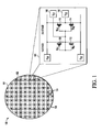
- FIG. 1 is a schematic diagram of an embodiment of a semiconductor device including a circuit that can be used to indicate transistor mismatch.
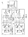
- FIG. 2 is a schematic diagram of an embodiment of a circuit that can be used to characterize transistor mismatch in the semiconductor device of FIG. 1 .
- FIG. 3 is a schematic diagram of another embodiment of a circuit that can be used to characterize transistor mismatch in the semiconductor device of FIG. 1 .
- Embodiments of systems and methods disclosed herein provide a circuit that generates a large, easy to measure output voltage that depends only on mismatch between metal-oxide-semiconductor field-effect transistors (MOSFET) in one inverter stage and transistors in another inverter stage.
- the circuit can be located in unused portions of a semiconductor wafer, or implemented in one or more integrated circuit dies on the wafer to enable cost-effective, reliable monitoring and control of transistor mismatch during fabrication to increase yield and device reliability.
- a semiconductor device 100 that includes wafer 101 on which a plurality of semiconductor die structures 102 are formed.
- Transistor mismatch circuits 104 can be formed anywhere along a grid of horizontal and/or vertical scribe streets 105 between the die structures 102 even though circuits 104 are shown at the intersections of horizontal and vertical scribe streets 105. Circuits 104 can also be formed in one or more die structures 102 in addition to or instead of being formed in scribe streets 105.
- Circuits 104 can include first P-type metal oxide semiconductor (PMOS) transistor 108, second PMOS transistor 110, first N-type metal oxide semiconductor NMOS transistor 112, and second NMOS transistor 114.
- Transistors 108, 110, 112, 114 each can have a source electrode, a drain electrode, a gate electrode, and a body electrode.
- the gate electrodes of first and second PMOS transistors 108, 110 and first and second NMOS transistors 112, 114 are coupled to the drain electrodes of first PMOS transistor 108 and first NMOS transistor 112.
- the drain electrode of second PMOS transistor 110 is coupled to the drain electrode of second NMOS transistor 114.
- the first output terminal Vo1 is coupled to the drain electrodes of first PMOS transistor 108 and first NMOS transistor 112.
- the second output terminal Vo2 is coupled to the drain electrodes of second PMOS transistor 110 and second NMOS transistor 114.
- Voltage supply Vdd is coupled to the source and bulk electrodes of first and second PMOS transistors 108, 110.
- Voltage supply Vss is coupled to the source and bulk electrodes of first and second NMOS transistors 112, 114.
- the difference between voltage at first output terminal Vo1 106 and voltage at second output terminal Vo2 116 indicates mismatch between the transistors 108, 110 112, 114.
- First PMOS and NMOS transistors 108, 112 form a self-biased inverter circuit.
- Second PMOS and NMOS transistors 110, 114 form a second stage inverter circuit that amplifies transistor mismatch of the self-biased inverter circuit.
- the mismatch measurements can be used to characterize transistors on wafer 101 right after wafer 101 is manufactured. Since it is desirable for similar types of transistors on semiconductor device 100 to have the same or similar characteristics, corrective action can be taken in subsequent manufacturing steps to reduce the differences between the transistors on wafers 101 if the mismatch characteristics are not acceptable.
- the difference between the voltages at the first and second output terminals 106, 116 is due to mismatch between first and second PMOS transistors 108, 110, and/or first and second NMOS transistors 112, 114.
- transistors 108, 110, 112, 114 can be varied to accentuate differences between transistors 108, 110, 112, 114.
- transistors 108, 110, 112, 114 can be formed with minimum length and width according to design rules for the process technology.
- the width of minimum length first and second PMOS transistors 108, 110 can be selected to have current drive capability comparable to first and second NMOS transistors 112, 114.
- the length and/or width for NMOS transistors 112, 114 can be formed to be greater than the minimum according to design rules for the process technology and the length for PMOS transistors 108, 110 can be the same as for NMOS transistors 112, 114 while the width for PMOS transistors 108, 110 can be scaled to give current drive comparable to NMOS transistors 112, 114.
- the minimum length for NMOS transistors 112, 114 can be used in circuit 104 with widths scaled to four or nine times the minimum width, or other suitable scale factor with minimum length for PMOS transistors 108, 110 with widths scaled to have current drive capability comparable to first and second NMOS transistors 112, 114.
- FIG. 2 is a schematic diagram of an embodiment of a circuit 200 that can be used to characterize transistor mismatch on semiconductor device 100 of FIG. 1 that comprises a plurality of transistor mismatch circuits 202, a plurality of absolute value circuits 204,and a characterization circuit 206 formed on semiconductor wafer 101.
- Characterization circuit 206 is coupled to receive input provided by a mismatch circuit 202 and absolute value circuit 204 and is configured to output a standard deviation of mismatch between transistors 208/212, 210/214 in a mismatch circuit 202.
- Transistor mismatch circuit 202 outputs values Vo1 and Vo2 and the difference between these output voltages is indicative of mismatch between PMOS transistors 208/212 and between NMOS transistors 212, 214.
- Absolute value circuit 204 and characterization circuit 206 receive the output of a mismatch circuit 202 and provides a value indicating the standard deviation of the mismatch between the transistors 208/212, 210/214.
- Characterization circuit 206 can be implemented as a summing amplifier that includes operational amplifier 232 coupled in parallel to resistor 230. Resistors 228 are coupled in series between respective transistor mismatch circuits 202 and absolute value circuits 204 and the summing amplifier. Resistor 230 has a value of R ohms and resistors 228 have a value equal to the value of the first resistor times the number of transistor mismatch circuits times the square root of 2 divided by pi (2/ ⁇ ) to determine the standard deviation of mismatch between transistors 208/212, 210/214 in the mismatch circuits 202. Note that other types of characterization circuits 206 can be implemented on semiconductor device 100 instead of or in addition to a summing amplifier to provide indicators or measurements of characteristics of transistor mismatch other than standard deviation.
- Transistor mismatch circuits 202 are similar to transistor mismatch circuits 104 of FIG. 1 and include a first stage inverter circuit with PMOS transistor 208 and NMOS transistor 210. A drain electrode of PMOS transistor 208 is coupled to a drain electrode of NMOS transistor 210. A second stage inverter circuit forming a second stage of mismatch circuit 202 includes PMOS transistor 212 and NMOS transistor 214. A drain electrode of PMOS transistor 212 is coupled to a drain electrode of NMOS transistor 214. A first output voltage Vo1 is coupled between the drain electrodes of first PMOS transistor 208 and first NMOS transistor 210 and to the gate electrodes of PMOS transistors 208, 212 and NMOS transistors 210, 214.
- a second output voltage Vo2 is coupled between the drain electrodes of second PMOS transistor 212 and second NMOS transistor 214.
- Source and bulk electrodes of PMOS transistors 208, 212 are coupled to Vdd, and source and bulk electrodes of NMOS transistors 210, 214 are coupled to Vss.
- a plurality of absolute value circuits 204 can be coupled between respective transistor mismatch circuits 202 and the characterization circuit 206.
- absolute value circuits 204 can include comparator 216 that has a first input coupled to the first output voltage Vo1 of transistor mismatch circuits 202.
- a second input of each comparator 216 is coupled to a respective second output voltage Vo2 from the transistor mismatch circuit 202.
- Comparator 216 provides an output (denoted as s1...sN for respective N-number of comparators) that is used to select inputs to respective unity gain buffer 226.
- Unity gain buffers 226 are configured to receive first and second inputs, and to provide an output that indicates the absolute value of the difference between the output voltages Vo1 and Vo2 of the respective transistor mismatch circuit 202.
- the first input of unity gain buffer 226 is coupled to a first set of switches 218, 220 that operate based on the output of comparator 216.
- Switch 218 closes and switch 220 opens to provide a first output voltage Vo1 to a first input of unity gain buffer 226 when a first output voltage is less than a second output voltage.
- Switch 218 opens and switch 220 closes to provide a second output voltage Vo2 to the first input of unity gain buffer 226 when a second output voltage is less than a first output voltage.
- the second input of unity gain buffer 226 is coupled to a second set of switches 222, 224 that operate based on the output of comparator 216.
- Switch 222 closes and switch 224 opens to provide a second output voltage Vo2 to the second input of the third comparator when a first output voltage is less than a second output voltage.
- Switch 222 opens and switch 224 closes to provide a first output voltage Vo1 to the second input of unity gain buffer 226 when a first output voltage is greater than a second output voltage.
- FIG. 3 is a schematic diagram of another embodiment of a circuit 300 that can be used to characterize transistor mismatch that includes one or more transistor mismatch circuits 202, one or more absolute value circuits 302, and characterization circuit 206 formed on semiconductor wafer 101.
- absolute value circuits 302 are coupled between respective transistor mismatch circuits 202 and characterization circuit 206.
- Absolute value circuits 302 include resistor 304 coupled between a first output voltage Vo1 and a first input of operational amplifier 310.
- Resistor 306 is coupled between a second output voltage Vo2 and a second input of operational amplifier 310.
- Resistor 308 is coupled between the first input of operational amplifier 310 and an output of operational amplifier 310.
- Resistor 312 is coupled between the second input of operational amplifier 310 and ground.
- Resistor 314 is coupled between the output of operational amplifier 310 and a first input of operational amplifier 328.
- Resistor 316 is coupled between the output of operational amplifier 310 and a first input of operational amplifier 330.
- Resistor 318 is coupled between the first input of operational amplifier 330 and a diode 324 and one terminal of a resistor 320. The other terminal of resistor 320 is coupled to the first input of operational amplifier 328. Diode 324 is coupled between one terminal of resistor 318 and the output of operational amplifier 328. Diode 326 is coupled between the output of operational amplifier 328 and the first input of operational amplifier 328. A second input of operational amplifier 328 is coupled to ground. Resistor 332 coupled between the first input of operational amplifier 330 and the output of operational amplifier 330. A second input of operational amplifier 330 is coupled to ground. Characterization circuit 206 is summing amplifier that includes operational amplifier 232 coupled in parallel to resistor 230. The first input of operational amplifier 232 receives output of absolute value circuits 302, connected via resistors 228. The second input of operational amplifier 232 is coupled to ground.
- Characterization circuit 206 is configured to output a standard deviation of mismatch between transistors 208/212, 210/214 in the mismatch circuits 202.
- the transistor mismatch circuits 202 outputs values Vo1 and Vo2 and the difference between these output voltages is indicative of mismatch between PMOS transistors 208/212 and between NMOS transistors 212, 214.
- Characterization circuit 206 receives the output of mismatch circuits 202 through absolute value circuits 302 and provides a value indicating the standard deviation of the mismatch between the transistors 208/212, 210/214.
- Characterization circuit 206 can be implemented as a summing amplifier that includes operational amplifier 232 coupled in parallel to resistor 230. Resistors 228 are coupled in series between respective absolute value circuits 302 and the summing amplifier. Resistor 230 has a value of R ohms and resistors 228 have a value equal to the value of the first resistor times the number of transistor mismatch circuits times the square root of 2 divided by pi (2/ ⁇ ) to determine the standard deviation of mismatch between transistors 208/212, 210/214 in the mismatch circuits 202. Note that other types of characterization circuits 206 can be implemented on semiconductor device 100 instead of or in addition to a summing amplifier to provide indicators or measurements of characteristics of transistor mismatch other than standard deviation.
- Transistor mismatch circuits 202 are similar to transistor mismatch circuits 104 of FIG. 1 and include a first stage inverter circuit with PMOS transistor 208 and NMOS transistor 210. A drain electrode of PMOS transistor 208 is coupled to a drain electrode of NMOS transistor 210. A second stage inverter circuit forming a second stage of mismatch circuit 202 includes PMOS transistor 212 and NMOS transistor 214. A drain electrode of PMOS transistor 212 is coupled to a drain electrode of NMOS transistor 214. A first output voltage Vo1 is coupled between the drain electrodes of first PMOS transistor 208 and first NMOS transistor 210 and to the gate electrodes of PMOS transistors 208, 212 and NMOS transistors 210, 214.
- a second output voltage Vo2 is coupled between the drain electrode of second PMOS transistor 212 and the drain electrode of the second NMOS transistor 214.
- Source and bulk electrodes of PMOS transistors 208, 212 are coupled to Vdd
- source and bulk electrodes of NMOS transistors 210, 214 are coupled to Vss.
- One or more circuits 200, 300 can be formed with one or more transistor mismatch circuits 104, 202, absolute value circuits 204, 302 and summing amplifier or other characterization circuit 206 in various locations in scribe streets 105 and/or in IC die 102 on semiconductor wafer 101 ( FIG. 1 ).
- supply voltages Vdd and Vss can be applied to the plurality of transistor mismatch circuits 104, 202 simultaneously during probe testing. Output of the characterization circuit 206 can be measured with another probe while the supply voltages are applied to the transistor mismatch circuits 104, 202.
- Each signal described herein may be designed as positive or negative logic, where negative logic can be indicated by a bar over the signal name or an asterix (*) following the name.
- negative logic the signal is active low where the logically true state corresponds to a logic level zero.
- positive logic the signal is active high where the logically true state corresponds to a logic level one.
- any of the signals described herein can be designed as either negative or positive logic signals. Therefore, in alternate embodiments, those signals described as positive logic signals may be implemented as negative logic signals, and those signals described as negative logic signals may be implemented as positive logic signals.
- circuits described herein can be implemented using any type of MOS transistor, such as standard bulk transistors, silicon on insulator transistors (with or without a body contact), and multi-gate FinFET structures, to name a few. Accordingly, the specification and figures are to be regarded in an illustrative rather than a restrictive sense, and all such modifications are intended to be included within the scope of the present disclosure. Any benefits, advantages, or solutions to problems that are described herein with regard to specific embodiments are not intended to be construed as a critical, required, or essential feature or element of any or all the claims.
- Coupled is not intended to be limited to a direct coupling or a mechanical coupling.
Landscapes
- Semiconductor Integrated Circuits (AREA)
- Metal-Oxide And Bipolar Metal-Oxide Semiconductor Integrated Circuits (AREA)
- Engineering & Computer Science (AREA)
- Automation & Control Theory (AREA)
- Manufacturing & Machinery (AREA)
Abstract
Description
- This application is related to United States Patent Application Serial No. _____ (Attorney Docket No. RA48748ZC), filed on even date, entitled "_____," naming Colin McAndrew and Michael Zunino as inventors, and assigned to the current assignee hereof.
- This disclosure relates generally to electronic circuits, and more specifically, to circuits for characterizing transistor mismatch.
- MOSFET mismatch is a leading cause of yield loss for analog circuits. Mismatch can vary over time in a manufacturing process, but characterization and on-going monitoring are difficult as they can, if the amount of mismatch is small, require precision and/or time-consuming measurements that are not available or are undesirable in a manufacturing environment.
- Direct drain current mismatch measurements, including over bias and geometry, can be used for mismatch characterization via a technique known as backward propagation of variance (BPV). In other approaches, threshold voltage and gain factor mismatch can be used for characterization and/or circuit modeling purposes. Whatever data are used, the test structures for mismatch characterization must be laid out very carefully and the measurements must be done extremely accurately because for precision circuits, mismatches of the order of 0.1% are important (e.g. for a 10 bit data converter, 210=1024 so the least significant bit needs to be accurate to order 0.1%).
- Because of the need for highly symmetric device layouts and highly precise measurements, mismatch characterization is difficult and has primarily been done in a lab and not a production test environment. This means that mismatch has often not been tracked over time.
- The present disclosure is illustrated by way of example and is not limited by the accompanying figures, in which like references indicate similar elements. Elements in the figures are illustrated for simplicity and clarity and have not necessarily been drawn to scale.
-
FIG. 1 is a schematic diagram of an embodiment of a semiconductor device including a circuit that can be used to indicate transistor mismatch. -
FIG. 2 is a schematic diagram of an embodiment of a circuit that can be used to characterize transistor mismatch in the semiconductor device ofFIG. 1 . -
FIG. 3 is a schematic diagram of another embodiment of a circuit that can be used to characterize transistor mismatch in the semiconductor device ofFIG. 1 . - Embodiments of systems and methods disclosed herein provide a circuit that generates a large, easy to measure output voltage that depends only on mismatch between metal-oxide-semiconductor field-effect transistors (MOSFET) in one inverter stage and transistors in another inverter stage. The circuit can be located in unused portions of a semiconductor wafer, or implemented in one or more integrated circuit dies on the wafer to enable cost-effective, reliable monitoring and control of transistor mismatch during fabrication to increase yield and device reliability.
- Referring to
FIG. 1 , asemiconductor device 100 is shown that includeswafer 101 on which a plurality ofsemiconductor die structures 102 are formed.Transistor mismatch circuits 104 can be formed anywhere along a grid of horizontal and/or vertical scribestreets 105 between the diestructures 102 even thoughcircuits 104 are shown at the intersections of horizontal and vertical scribestreets 105.Circuits 104 can also be formed in one or more diestructures 102 in addition to or instead of being formed inscribe streets 105. -
Circuits 104 can include first P-type metal oxide semiconductor (PMOS)transistor 108,second PMOS transistor 110, first N-type metal oxidesemiconductor NMOS transistor 112, andsecond NMOS transistor 114.Transistors second PMOS transistors second NMOS transistors first PMOS transistor 108 andfirst NMOS transistor 112. The drain electrode ofsecond PMOS transistor 110 is coupled to the drain electrode ofsecond NMOS transistor 114. The first output terminal Vo1 is coupled to the drain electrodes offirst PMOS transistor 108 andfirst NMOS transistor 112. The second output terminal Vo2 is coupled to the drain electrodes ofsecond PMOS transistor 110 andsecond NMOS transistor 114. - Voltage supply Vdd is coupled to the source and bulk electrodes of first and
second PMOS transistors second NMOS transistors - The difference between voltage at first
output terminal Vo1 106 and voltage at secondoutput terminal Vo2 116 indicates mismatch between thetransistors NMOS transistors NMOS transistors - The mismatch measurements can be used to characterize transistors on
wafer 101 right afterwafer 101 is manufactured. Since it is desirable for similar types of transistors onsemiconductor device 100 to have the same or similar characteristics, corrective action can be taken in subsequent manufacturing steps to reduce the differences between the transistors onwafers 101 if the mismatch characteristics are not acceptable. - The difference between the voltages at the first and
second output terminals second PMOS transistors second NMOS transistors - The geometry of the
transistors transistors transistors second PMOS transistors second NMOS transistors NMOS transistors PMOS transistors NMOS transistors PMOS transistors NMOS transistors NMOS transistors circuit 104 with widths scaled to four or nine times the minimum width, or other suitable scale factor with minimum length forPMOS transistors second NMOS transistors -
FIG. 2 is a schematic diagram of an embodiment of acircuit 200 that can be used to characterize transistor mismatch onsemiconductor device 100 ofFIG. 1 that comprises a plurality oftransistor mismatch circuits 202, a plurality ofabsolute value circuits 204,and acharacterization circuit 206 formed onsemiconductor wafer 101.Characterization circuit 206 is coupled to receive input provided by amismatch circuit 202 andabsolute value circuit 204 and is configured to output a standard deviation of mismatch betweentransistors 208/212, 210/214 in amismatch circuit 202.Transistor mismatch circuit 202 outputs values Vo1 and Vo2 and the difference between these output voltages is indicative of mismatch betweenPMOS transistors 208/212 and betweenNMOS transistors 212, 214.Absolute value circuit 204 andcharacterization circuit 206 receive the output of amismatch circuit 202 and provides a value indicating the standard deviation of the mismatch between thetransistors 208/212, 210/214. -
Characterization circuit 206 can be implemented as a summing amplifier that includesoperational amplifier 232 coupled in parallel toresistor 230.Resistors 228 are coupled in series between respectivetransistor mismatch circuits 202 andabsolute value circuits 204 and the summing amplifier.Resistor 230 has a value of R ohms andresistors 228 have a value equal to the value of the first resistor times the number of transistor mismatch circuits times the square root of 2 divided by pi (2/π) to determine the standard deviation of mismatch betweentransistors 208/212, 210/214 in themismatch circuits 202. Note that other types ofcharacterization circuits 206 can be implemented onsemiconductor device 100 instead of or in addition to a summing amplifier to provide indicators or measurements of characteristics of transistor mismatch other than standard deviation. -
Transistor mismatch circuits 202 are similar totransistor mismatch circuits 104 ofFIG. 1 and include a first stage inverter circuit withPMOS transistor 208 andNMOS transistor 210. A drain electrode ofPMOS transistor 208 is coupled to a drain electrode ofNMOS transistor 210. A second stage inverter circuit forming a second stage ofmismatch circuit 202 includes PMOS transistor 212 andNMOS transistor 214. A drain electrode of PMOS transistor 212 is coupled to a drain electrode ofNMOS transistor 214. A first output voltage Vo1 is coupled between the drain electrodes offirst PMOS transistor 208 andfirst NMOS transistor 210 and to the gate electrodes ofPMOS transistors 208, 212 andNMOS transistors second NMOS transistor 214. Source and bulk electrodes ofPMOS transistors 208, 212 are coupled to Vdd, and source and bulk electrodes ofNMOS transistors - A plurality of
absolute value circuits 204 can be coupled between respectivetransistor mismatch circuits 202 and thecharacterization circuit 206. In some embodiments,absolute value circuits 204 can includecomparator 216 that has a first input coupled to the first output voltage Vo1 oftransistor mismatch circuits 202. A second input of eachcomparator 216 is coupled to a respective second output voltage Vo2 from thetransistor mismatch circuit 202.Comparator 216 provides an output (denoted as s1...sN for respective N-number of comparators) that is used to select inputs to respectiveunity gain buffer 226. - Unity
gain buffers 226 are configured to receive first and second inputs, and to provide an output that indicates the absolute value of the difference between the output voltages Vo1 and Vo2 of the respectivetransistor mismatch circuit 202. The first input ofunity gain buffer 226 is coupled to a first set ofswitches comparator 216.Switch 218 closes and switch 220 opens to provide a first output voltage Vo1 to a first input ofunity gain buffer 226 when a first output voltage is less than a second output voltage.Switch 218 opens and switch 220 closes to provide a second output voltage Vo2 to the first input ofunity gain buffer 226 when a second output voltage is less than a first output voltage. - The second input of
unity gain buffer 226 is coupled to a second set ofswitches comparator 216.Switch 222 closes and switch 224 opens to provide a second output voltage Vo2 to the second input of the third comparator when a first output voltage is less than a second output voltage.Switch 222 opens and switch 224 closes to provide a first output voltage Vo1 to the second input ofunity gain buffer 226 when a first output voltage is greater than a second output voltage. -
FIG. 3 is a schematic diagram of another embodiment of acircuit 300 that can be used to characterize transistor mismatch that includes one or moretransistor mismatch circuits 202, one or moreabsolute value circuits 302, andcharacterization circuit 206 formed onsemiconductor wafer 101. - In the embodiment shown,
absolute value circuits 302 are coupled between respectivetransistor mismatch circuits 202 andcharacterization circuit 206.Absolute value circuits 302 includeresistor 304 coupled between a first output voltage Vo1 and a first input ofoperational amplifier 310.Resistor 306 is coupled between a second output voltage Vo2 and a second input ofoperational amplifier 310.Resistor 308 is coupled between the first input ofoperational amplifier 310 and an output ofoperational amplifier 310.Resistor 312 is coupled between the second input ofoperational amplifier 310 and ground.Resistor 314 is coupled between the output ofoperational amplifier 310 and a first input ofoperational amplifier 328.Resistor 316 is coupled between the output ofoperational amplifier 310 and a first input ofoperational amplifier 330.Resistor 318 is coupled between the first input ofoperational amplifier 330 and adiode 324 and one terminal of aresistor 320. The other terminal ofresistor 320 is coupled to the first input ofoperational amplifier 328.Diode 324 is coupled between one terminal ofresistor 318 and the output ofoperational amplifier 328.Diode 326 is coupled between the output ofoperational amplifier 328 and the first input ofoperational amplifier 328. A second input ofoperational amplifier 328 is coupled to ground.Resistor 332 coupled between the first input ofoperational amplifier 330 and the output ofoperational amplifier 330. A second input ofoperational amplifier 330 is coupled to ground.Characterization circuit 206 is summing amplifier that includesoperational amplifier 232 coupled in parallel toresistor 230. The first input ofoperational amplifier 232 receives output ofabsolute value circuits 302, connected viaresistors 228. The second input ofoperational amplifier 232 is coupled to ground. -
Characterization circuit 206 is configured to output a standard deviation of mismatch betweentransistors 208/212, 210/214 in themismatch circuits 202. Thetransistor mismatch circuits 202 outputs values Vo1 and Vo2 and the difference between these output voltages is indicative of mismatch betweenPMOS transistors 208/212 and betweenNMOS transistors 212, 214.Characterization circuit 206 receives the output ofmismatch circuits 202 throughabsolute value circuits 302 and provides a value indicating the standard deviation of the mismatch between thetransistors 208/212, 210/214. -
Characterization circuit 206 can be implemented as a summing amplifier that includesoperational amplifier 232 coupled in parallel toresistor 230.Resistors 228 are coupled in series between respectiveabsolute value circuits 302 and the summing amplifier.Resistor 230 has a value of R ohms andresistors 228 have a value equal to the value of the first resistor times the number of transistor mismatch circuits times the square root of 2 divided by pi (2/π) to determine the standard deviation of mismatch betweentransistors 208/212, 210/214 in themismatch circuits 202. Note that other types ofcharacterization circuits 206 can be implemented onsemiconductor device 100 instead of or in addition to a summing amplifier to provide indicators or measurements of characteristics of transistor mismatch other than standard deviation. -
Transistor mismatch circuits 202 are similar totransistor mismatch circuits 104 ofFIG. 1 and include a first stage inverter circuit withPMOS transistor 208 andNMOS transistor 210. A drain electrode ofPMOS transistor 208 is coupled to a drain electrode ofNMOS transistor 210. A second stage inverter circuit forming a second stage ofmismatch circuit 202 includes PMOS transistor 212 andNMOS transistor 214. A drain electrode of PMOS transistor 212 is coupled to a drain electrode ofNMOS transistor 214. A first output voltage Vo1 is coupled between the drain electrodes offirst PMOS transistor 208 andfirst NMOS transistor 210 and to the gate electrodes ofPMOS transistors 208, 212 andNMOS transistors second NMOS transistor 214. Source and bulk electrodes ofPMOS transistors 208, 212 are coupled to Vdd, and source and bulk electrodes ofNMOS transistors - One or
more circuits transistor mismatch circuits absolute value circuits other characterization circuit 206 in various locations inscribe streets 105 and/or in IC die 102 on semiconductor wafer 101 (FIG. 1 ). - Once
wafer 101 is processed, supply voltages Vdd and Vss can be applied to the plurality oftransistor mismatch circuits characterization circuit 206 can be measured with another probe while the supply voltages are applied to thetransistor mismatch circuits - Because the apparatus implementing the present disclosure is, apart from
transistor mismatch circuits - Each signal described herein may be designed as positive or negative logic, where negative logic can be indicated by a bar over the signal name or an asterix (*) following the name. In the case of a negative logic signal, the signal is active low where the logically true state corresponds to a logic level zero. In the case of a positive logic signal, the signal is active high where the logically true state corresponds to a logic level one. Note that any of the signals described herein can be designed as either negative or positive logic signals. Therefore, in alternate embodiments, those signals described as positive logic signals may be implemented as negative logic signals, and those signals described as negative logic signals may be implemented as positive logic signals.
- Although the disclosure has been described with respect to specific conductivity types or polarity of potentials, skilled artisans appreciate that conductivity types and polarities of potentials may be reversed.
- Moreover, the terms "front," "back," "top," "bottom," "over," "under" and the like in the description and in the claims, if any, are used for descriptive purposes and not necessarily for describing permanent relative positions. It is understood that the terms so used are interchangeable under appropriate circumstances such that the embodiments of the disclosure described herein are, for example, capable of operation in other orientations than those illustrated or otherwise described herein.
- Although the disclosure is described herein with reference to specific embodiments, various modifications and changes can be made without departing from the scope of the present disclosure as set forth in the claims below. For example, the circuits described herein can be implemented using any type of MOS transistor, such as standard bulk transistors, silicon on insulator transistors (with or without a body contact), and multi-gate FinFET structures, to name a few. Accordingly, the specification and figures are to be regarded in an illustrative rather than a restrictive sense, and all such modifications are intended to be included within the scope of the present disclosure. Any benefits, advantages, or solutions to problems that are described herein with regard to specific embodiments are not intended to be construed as a critical, required, or essential feature or element of any or all the claims.
- The term "coupled," as used herein, is not intended to be limited to a direct coupling or a mechanical coupling.
- Furthermore, the terms "a" or "an," as used herein, are defined as one or more than one. Also, the use of introductory phrases such as "at least one" and "one or more" in the claims should not be construed to imply that the introduction of another claim element by the indefinite articles "a" or "an" limits any particular claim containing such introduced claim element to disclosures containing only one such element, even when the same claim includes the introductory phrases "one or more" or "at least one" and indefinite articles such as "a" or "an." The same holds true for the use of definite articles.
Unless stated otherwise, terms such as "first" and "second" are used to arbitrarily distinguish between the elements such terms describe. Thus, these terms are not necessarily intended to indicate temporal or other prioritization of such elements.
Claims (15)
- A semiconductor device comprising:a summing amplifier (206);a plurality of transistor mismatch circuits (202), wherein the transistor mismatch circuits output a value indicative of mismatch between transistors in a respective one of the transistor mismatch circuits; andoutput from the transistor mismatch circuits (202) coupled to an input of the summing amplifier (206), wherein the summing amplifier provides a value indicating a standard deviation of the mismatch between the transistors.
- The semiconductor device of claim 1 further comprising:the summing amplifier (206) includes a first operational amplifier (232) coupled in parallel to a first resistor (230); anda plurality of second resistors (228) coupled in series between respective transistor mismatch circuits and the summing amplifier.
- The semiconductor device of claim 2 further comprising:the first resistor (230) has a value of R ohms; andthe second resistors (228) have a value equal to the value of the first resistor times the number of transistor mismatch circuits times the square root of 2 divided by pi (√(2/π)).
- The semiconductor device of any one of the preceding claims, wherein the transistor mismatch circuits (202) comprise:a first inverter circuit including a first PMOS transistor (208) and a first NMOS transistor (210), a drain electrode of the first PMOS transistor coupled to a drain electrode of the first NMOS transistor;a second inverter circuit including a second PMOS transistor (212) and a second NMOS transistor (214), a drain electrode of the second PMOS transistor coupled to a drain electrode of the second NMOS transistor;a first output voltage Vo1 coupled to gate electrodes of the first and second PMOS and NMOS transistors, and between the drain electrode of the first PMOS transistor (208) and the drain electrode of the first NMOS transistor (210) to self-bias the first inverter circuit; anda second output voltage Vo2 coupled between the drain electrode of the second PMOS transistor and the drain electrode of the second NMOS transistor.
- The semiconductor device of any one of the preceding claims further comprising:a plurality of absolute value circuits (204) coupled between respective transistor mismatch circuits (202) and the summing amplifier (206).
- The semiconductor device of claim 5, wherein the absolute value circuits include a comparator (216) that has
a first input coupled to a respective first output voltage Vo1 of one of the transistor mismatch circuits,
a second input coupled to a respective second output voltage Vo2 from one of the transistor mismatch circuits, and
an output that is used to select inputs to a unity gain buffer (226); and
a unity gain buffer (226) configured to receive a first input and a second input, and to provide the unity gain buffer output indicating the absolute value of the difference between the second output voltage and the first output voltage of the respective transistor mismatch circuit,
the first input of the unity gain buffer (226) is coupled to a first set of switches (218, 220) that operate based on the output of the comparator to provide the first output voltage to the first input of the unity gain buffer (226) when the first output voltage is less than the second output voltage, and to provide the second output voltage to the first input of the unity gain buffer (226) when the second output voltage is less than the first output voltage, and
the second input of the unity gain buffer (226) is coupled to a second set of switches (222), (224) that operate based on the output of the comparator (216) to provide the first output voltage to the second input of the unity gain buffer (226) when the first output voltage is greater than the second output voltage, and to provide the second output voltage to the second input of the unity gain buffer (226) when the second output voltage is greater than the first output voltage. - The semiconductor device of claim 5 or 6, wherein the absolute value circuits further include:a second resistor (304) coupled between the first output voltage Vo1 and a first input of a second operational amplifier (310);a third resistor (306) coupled between the second output voltage Vo2 and a second input of the second operational amplifier (310);a fourth resistor (308) coupled between the first input of the second operational amplifier (310) and an output of the second operational amplifier (310);a fifth resistor (312) coupled between the second input of the second operational amplifier (310) and ground;a sixth resistor (314) coupled between the output of the second operational amplifier (310) and a first input of a third operational amplifier (328);a seventh resistor (316) coupled between the output of the second operational amplifier 310) and a first input of a fourth operational amplifier 330;an eighth resistor (318) coupled between the first input of the second operational amplifier (330) and a diode (324);a ninth resistor (320) including one terminal coupled between the eighth resistor (318) and diode (324), another terminal coupled to one input of the third operational amplifier (328);a first diode (324) coupled between the output of the third operational amplifier (328) and the eighth resistor (318);a second diode (326) coupled between the first input of the third operational amplifier (328) and the output of the third operational amplifier (328);a second input of the third operational amplifier (328) is coupled to ground;a tenth resistor (332) coupled between the first input of the fourth operational amplifier (330) and the output of the fourth operational amplifier (330); anda second input of the fourth operational amplifier (330) is coupled to ground.
- The semiconductor device of claim 5,6 or 7 wherein the summing amplifier (206) includes a first operational amplifier (232) with a resistor (230) coupled between an output of the first operational amplifier and a first input of the first operational amplifier (232) and with a second input of the first operational amplifier (232) coupled to ground.
- A semiconductor device (100) comprising:a plurality of transistor mismatch circuits (104, 202) formed on a semiconductor wafer (101); anda characterization circuit (206) formed on the semiconductor wafer (101, the characterization circuit (206) is coupled to receive input provided by the mismatch circuits (104, 202) simultaneously and is configured to output a standard deviation of mismatch between transistors (208/212), (210/214) in the mismatch circuits (104, 202).
- The semiconductor device of claim 9 further comprising:a plurality of absolute value circuits (204, 302) coupled between respective transistor mismatch circuits (104, 202) and the characterization circuit (206), wherein the absolute value circuits (204, 302) are configured to receive input from the transistor mismatch circuits (104, 202) and to output an absolute value of the input.
- The semiconductor device of claim 9 or 10, the mismatch circuits (104, 202) comprising:a first PMOS transistor (208) and a first NMOS transistor (210) configured as a first stage inverter circuit; anda second PMOS transistor (212) and a second NMOS transistor (214) configured as a second stage inverter circuit that is coupled to the first inverter circuit.
- The semiconductor device of claim 9,10 or 11, further comprising:a plurality of resistors (228), wherein each of the resistors (228) is coupled between the output of a respective one of the absolute value circuits (204, 302) and the characterization circuit (206), and the value of the resistors (228) is proportional to the number of mismatch circuits (104, 202).
- The semiconductor device of claim 12, wherein the characterization circuit is a summing amplifier (206) that includes a first operational amplifier (232) with a resistor (230) coupled between an output of the first operational amplifier and a first input and a second input coupled to ground.
- The semiconductor device of claim 9,10,11,12 or 13 wherein the transistor mismatch circuits (202) comprise:a first inverter circuit including a first PMOS transistor (208) and a first NMOS transistor (210), a drain electrode of the first PMOS transistor (208) coupled to a drain electrode of the first NMOS transistor (210);a second inverter circuit including a second PMOS transistor (212) and a second NMOS transistor (214), a drain electrode of the second PMOS transistor (212) coupled to a drain electrode of the second NMOS transistor (214);a first output voltage Vo1 (106) coupled to gate electrodes of the first and second PMOS and NMOS transistors (208/212), (210/214), and between the drain electrode of the first PMOS transistor (208) and the drain electrode of the first NMOS transistor (210) to self-bias the first inverter circuit; anda second output voltage Vo2 (116) coupled between the drain electrode of the second PMOS transistor (212) and the drain electrode of the second NMOS transistor (214).
- The semiconductor device of claim 9,10,11,12,13 or 14 wherein the mismatch circuits (104, 202) are formed in at least one of: a scribe street (105) on the wafer (101), and in an integrated circuit die (102) on the wafer (101).
Applications Claiming Priority (1)
| Application Number | Priority Date | Filing Date | Title |
|---|---|---|---|
| US13/222,335 US9111894B2 (en) | 2011-08-31 | 2011-08-31 | MOFSET mismatch characterization circuit |
Related Parent Applications (2)
| Application Number | Title | Priority Date | Filing Date |
|---|---|---|---|
| US201113222335 Previously-Filed-Application | 2011-08-31 | ||
| US13/222,335 Previously-Filed-Application US9111894B2 (en) | 2011-08-31 | 2011-08-31 | MOFSET mismatch characterization circuit |
Publications (3)
| Publication Number | Publication Date |
|---|---|
| EP2565915A2 true EP2565915A2 (en) | 2013-03-06 |
| EP2565915A3 EP2565915A3 (en) | 2016-03-02 |
| EP2565915B1 EP2565915B1 (en) | 2020-10-07 |
Family
ID=47044740
Family Applications (1)
| Application Number | Title | Priority Date | Filing Date |
|---|---|---|---|
| EP12179305.3A Active EP2565915B1 (en) | 2011-08-31 | 2012-08-03 | MOSFET mismatch characterization circuit |
Country Status (4)
| Country | Link |
|---|---|
| US (1) | US9111894B2 (en) |
| EP (1) | EP2565915B1 (en) |
| KR (1) | KR101880765B1 (en) |
| TW (1) | TWI552242B (en) |
Families Citing this family (1)
| Publication number | Priority date | Publication date | Assignee | Title |
|---|---|---|---|---|
| US9135987B2 (en) * | 2013-07-01 | 2015-09-15 | Internatinal Business Machines Corporation | FinFET-based boosting supply voltage circuit and method |
Family Cites Families (21)
| Publication number | Priority date | Publication date | Assignee | Title |
|---|---|---|---|---|
| US3952185A (en) * | 1975-01-17 | 1976-04-20 | Philip Morris Incorporated | Standard deviation determining apparatus |
| JPH01138813A (en) | 1987-11-26 | 1989-05-31 | Toshiba Corp | Level conversion circuit |
| US4980580A (en) | 1989-03-27 | 1990-12-25 | Microelectronics And Computer Technology Corporation | CMOS interconnection circuit |
| US5041741A (en) | 1990-09-14 | 1991-08-20 | Ncr Corporation | Transient immune input buffer |
| JPH0746098A (en) | 1993-08-03 | 1995-02-14 | Nec Corp | Delay circuit |
| US5438287A (en) | 1994-06-01 | 1995-08-01 | United Memories Inc. | High speed differential current sense amplifier with positive feedback |
| JPH1140522A (en) | 1997-07-17 | 1999-02-12 | Rohm Co Ltd | Semiconductor wafer manufacturing method, semiconductor wafer manufactured by this method, semiconductor chip manufacturing method, semiconductor chip manufactured by this method, and IC card equipped with this semiconductor chip |
| JP3609977B2 (en) | 1999-07-15 | 2005-01-12 | シャープ株式会社 | Level shift circuit and image display device |
| JP3571013B2 (en) * | 2001-08-23 | 2004-09-29 | エルピーダメモリ株式会社 | Semiconductor device, driving method thereof, and setting method thereof |
| US6696800B2 (en) | 2002-01-10 | 2004-02-24 | Koninklijke Philips Electronics N.V. | High frequency electronic ballast |
| US7002241B1 (en) | 2003-02-12 | 2006-02-21 | National Semiconductor Corporation | Packaging of semiconductor device with a non-opaque cover |
| US7129566B2 (en) | 2004-06-30 | 2006-10-31 | Freescale Semiconductor, Inc. | Scribe street structure for backend interconnect semiconductor wafer integration |
| JP4096948B2 (en) * | 2005-02-01 | 2008-06-04 | セイコーエプソン株式会社 | Level shift circuit, electro-optical device using the same, and electronic apparatus |
| US7408372B2 (en) | 2006-06-08 | 2008-08-05 | International Business Machines Corporation | Method and apparatus for measuring device mismatches |
| US8115479B2 (en) | 2006-11-21 | 2012-02-14 | Hitachi Metals, Ltd. | Rotation-angle-detecting apparatus, rotating machine, and rotation-angle-detecting method |
| US7711998B2 (en) * | 2007-03-30 | 2010-05-04 | Infineon Technologies Ag | Test circuit arrangement |
| US7863965B2 (en) * | 2007-06-27 | 2011-01-04 | Hynix Semiconductor Inc. | Temperature sensor circuit and method for controlling the same |
| US7673195B2 (en) * | 2007-10-03 | 2010-03-02 | International Business Machines Corporation | Circuits and methods for characterizing device variation in electronic memory circuits |
| US8862426B2 (en) * | 2007-12-20 | 2014-10-14 | International Business Machines Corporation | Method and test system for fast determination of parameter variation statistics |
| US8183910B2 (en) | 2008-11-17 | 2012-05-22 | Taiwan Semiconductor Manufacturing Co., Ltd. | Circuit and method for a digital process monitor |
| KR20100078608A (en) * | 2008-12-30 | 2010-07-08 | 주식회사 동부하이텍 | Apparatus and method for testing mos transistors |
-
2011
- 2011-08-31 US US13/222,335 patent/US9111894B2/en active Active
-
2012
- 2012-08-03 EP EP12179305.3A patent/EP2565915B1/en active Active
- 2012-08-30 TW TW101131628A patent/TWI552242B/en active
- 2012-08-31 KR KR1020120096302A patent/KR101880765B1/en active Active
Non-Patent Citations (1)
| Title |
|---|
| None |
Also Published As
| Publication number | Publication date |
|---|---|
| KR101880765B1 (en) | 2018-07-20 |
| TW201320215A (en) | 2013-05-16 |
| KR20130024868A (en) | 2013-03-08 |
| US20130049788A1 (en) | 2013-02-28 |
| US9111894B2 (en) | 2015-08-18 |
| EP2565915A3 (en) | 2016-03-02 |
| EP2565915B1 (en) | 2020-10-07 |
| TWI552242B (en) | 2016-10-01 |
Similar Documents
| Publication | Publication Date | Title |
|---|---|---|
| US6894520B2 (en) | Semiconductor device and capacitance measurement method | |
| US8935117B2 (en) | Circuit and method for measuring voltage | |
| US8629693B2 (en) | Semiconductor integrated circuit with a chain of inverters | |
| US6501283B2 (en) | Circuit configuration for measuring the capacitance of structures in an integrated circuit | |
| US20140347083A1 (en) | Silicon-on-insulator (soi) body-contact pass gate structure | |
| CN110763972A (en) | Method for measuring threshold voltage of MOSFET | |
| US8729954B2 (en) | MOFSET mismatch characterization circuit | |
| US9111894B2 (en) | MOFSET mismatch characterization circuit | |
| US20140266290A1 (en) | Process detection circuit | |
| US10983160B2 (en) | Circuit and method for measuring working current of circuit module | |
| US6777708B1 (en) | Apparatus and methods for determining floating body effects in SOI devices | |
| US8456169B2 (en) | High speed measurement of random variation/yield in integrated circuit device testing | |
| EP2413149A1 (en) | Capacitance measurement in microchips | |
| Agarwal et al. | Rapid characterization of threshold voltage fluctuation in MOS devices | |
| CN109991526B (en) | Capacitance testing method under different voltage bias, and testing chip and system thereof | |
| US8064832B2 (en) | Method and test system for determining gate-to-body current in a floating body FET | |
| CN222167159U (en) | Circuit structure and chip for measuring on-resistance of MOS tube | |
| CN119171885B (en) | Chip process corner difference eliminating circuit and method and NAND flash memory chip | |
| Jain et al. | On-chip threshold voltage variability detector targeting supply of ring oscillator for characterizing local device mismatch | |
| CN203811768U (en) | Hot carrier testing circuit | |
| Ketchen et al. | Addressable arrays implemented with one metal level for MOSFET and resistor variability characterization | |
| JP2005055231A (en) | Method for inspecting on resistance in mos transistor | |
| EP3187885B1 (en) | A current sensing circuit and method | |
| CN210090563U (en) | Circuit unit for testing grid dynamic capacitance of inverter and test circuit | |
| CN103675398A (en) | Method for measuring NMOS (N-channel Metal Oxide Semiconductor) threshold voltage |
Legal Events
| Date | Code | Title | Description |
|---|---|---|---|
| PUAI | Public reference made under article 153(3) epc to a published international application that has entered the european phase |
Free format text: ORIGINAL CODE: 0009012 |
|
| AK | Designated contracting states |
Kind code of ref document: A2 Designated state(s): AL AT BE BG CH CY CZ DE DK EE ES FI FR GB GR HR HU IE IS IT LI LT LU LV MC MK MT NL NO PL PT RO RS SE SI SK SM TR |
|
| AX | Request for extension of the european patent |
Extension state: BA ME |
|
| PUAL | Search report despatched |
Free format text: ORIGINAL CODE: 0009013 |
|
| AK | Designated contracting states |
Kind code of ref document: A3 Designated state(s): AL AT BE BG CH CY CZ DE DK EE ES FI FR GB GR HR HU IE IS IT LI LT LU LV MC MK MT NL NO PL PT RO RS SE SI SK SM TR |
|
| AX | Request for extension of the european patent |
Extension state: BA ME |
|
| RIC1 | Information provided on ipc code assigned before grant |
Ipc: H01L 27/092 20060101ALN20160126BHEP Ipc: H01L 21/66 20060101AFI20160126BHEP |
|
| 17P | Request for examination filed |
Effective date: 20160902 |
|
| RBV | Designated contracting states (corrected) |
Designated state(s): AL AT BE BG CH CY CZ DE DK EE ES FI FR GB GR HR HU IE IS IT LI LT LU LV MC MK MT NL NO PL PT RO RS SE SI SK SM TR |
|
| RAP1 | Party data changed (applicant data changed or rights of an application transferred) |
Owner name: NXP USA, INC. |
|
| STAA | Information on the status of an ep patent application or granted ep patent |
Free format text: STATUS: EXAMINATION IS IN PROGRESS |
|
| 17Q | First examination report despatched |
Effective date: 20190319 |
|
| GRAP | Despatch of communication of intention to grant a patent |
Free format text: ORIGINAL CODE: EPIDOSNIGR1 |
|
| STAA | Information on the status of an ep patent application or granted ep patent |
Free format text: STATUS: GRANT OF PATENT IS INTENDED |
|
| RIC1 | Information provided on ipc code assigned before grant |
Ipc: H01L 27/092 20060101ALN20200603BHEP Ipc: H01L 21/66 20060101AFI20200603BHEP |
|
| RIC1 | Information provided on ipc code assigned before grant |
Ipc: H01L 27/092 20060101ALN20200608BHEP Ipc: H01L 21/66 20060101AFI20200608BHEP |
|
| INTG | Intention to grant announced |
Effective date: 20200630 |
|
| GRAS | Grant fee paid |
Free format text: ORIGINAL CODE: EPIDOSNIGR3 |
|
| GRAA | (expected) grant |
Free format text: ORIGINAL CODE: 0009210 |
|
| STAA | Information on the status of an ep patent application or granted ep patent |
Free format text: STATUS: THE PATENT HAS BEEN GRANTED |
|
| AK | Designated contracting states |
Kind code of ref document: B1 Designated state(s): AL AT BE BG CH CY CZ DE DK EE ES FI FR GB GR HR HU IE IS IT LI LT LU LV MC MK MT NL NO PL PT RO RS SE SI SK SM TR |
|
| REG | Reference to a national code |
Ref country code: GB Ref legal event code: FG4D |
|
| REG | Reference to a national code |
Ref country code: CH Ref legal event code: EP Ref country code: AT Ref legal event code: REF Ref document number: 1322049 Country of ref document: AT Kind code of ref document: T Effective date: 20201015 |
|
| REG | Reference to a national code |
Ref country code: IE Ref legal event code: FG4D |
|
| REG | Reference to a national code |
Ref country code: DE Ref legal event code: R096 Ref document number: 602012072641 Country of ref document: DE |
|
| REG | Reference to a national code |
Ref country code: NL Ref legal event code: MP Effective date: 20201007 |
|
| REG | Reference to a national code |
Ref country code: AT Ref legal event code: MK05 Ref document number: 1322049 Country of ref document: AT Kind code of ref document: T Effective date: 20201007 |
|
| PG25 | Lapsed in a contracting state [announced via postgrant information from national office to epo] |
Ref country code: GR Free format text: LAPSE BECAUSE OF FAILURE TO SUBMIT A TRANSLATION OF THE DESCRIPTION OR TO PAY THE FEE WITHIN THE PRESCRIBED TIME-LIMIT Effective date: 20210108 Ref country code: RS Free format text: LAPSE BECAUSE OF FAILURE TO SUBMIT A TRANSLATION OF THE DESCRIPTION OR TO PAY THE FEE WITHIN THE PRESCRIBED TIME-LIMIT Effective date: 20201007 Ref country code: FI Free format text: LAPSE BECAUSE OF FAILURE TO SUBMIT A TRANSLATION OF THE DESCRIPTION OR TO PAY THE FEE WITHIN THE PRESCRIBED TIME-LIMIT Effective date: 20201007 Ref country code: NO Free format text: LAPSE BECAUSE OF FAILURE TO SUBMIT A TRANSLATION OF THE DESCRIPTION OR TO PAY THE FEE WITHIN THE PRESCRIBED TIME-LIMIT Effective date: 20210107 Ref country code: NL Free format text: LAPSE BECAUSE OF FAILURE TO SUBMIT A TRANSLATION OF THE DESCRIPTION OR TO PAY THE FEE WITHIN THE PRESCRIBED TIME-LIMIT Effective date: 20201007 Ref country code: PT Free format text: LAPSE BECAUSE OF FAILURE TO SUBMIT A TRANSLATION OF THE DESCRIPTION OR TO PAY THE FEE WITHIN THE PRESCRIBED TIME-LIMIT Effective date: 20210208 |
|
| REG | Reference to a national code |
Ref country code: LT Ref legal event code: MG4D |
|
| PG25 | Lapsed in a contracting state [announced via postgrant information from national office to epo] |
Ref country code: IS Free format text: LAPSE BECAUSE OF FAILURE TO SUBMIT A TRANSLATION OF THE DESCRIPTION OR TO PAY THE FEE WITHIN THE PRESCRIBED TIME-LIMIT Effective date: 20210207 Ref country code: ES Free format text: LAPSE BECAUSE OF FAILURE TO SUBMIT A TRANSLATION OF THE DESCRIPTION OR TO PAY THE FEE WITHIN THE PRESCRIBED TIME-LIMIT Effective date: 20201007 Ref country code: AT Free format text: LAPSE BECAUSE OF FAILURE TO SUBMIT A TRANSLATION OF THE DESCRIPTION OR TO PAY THE FEE WITHIN THE PRESCRIBED TIME-LIMIT Effective date: 20201007 Ref country code: BG Free format text: LAPSE BECAUSE OF FAILURE TO SUBMIT A TRANSLATION OF THE DESCRIPTION OR TO PAY THE FEE WITHIN THE PRESCRIBED TIME-LIMIT Effective date: 20210107 Ref country code: SE Free format text: LAPSE BECAUSE OF FAILURE TO SUBMIT A TRANSLATION OF THE DESCRIPTION OR TO PAY THE FEE WITHIN THE PRESCRIBED TIME-LIMIT Effective date: 20201007 Ref country code: LV Free format text: LAPSE BECAUSE OF FAILURE TO SUBMIT A TRANSLATION OF THE DESCRIPTION OR TO PAY THE FEE WITHIN THE PRESCRIBED TIME-LIMIT Effective date: 20201007 Ref country code: PL Free format text: LAPSE BECAUSE OF FAILURE TO SUBMIT A TRANSLATION OF THE DESCRIPTION OR TO PAY THE FEE WITHIN THE PRESCRIBED TIME-LIMIT Effective date: 20201007 |
|
| PG25 | Lapsed in a contracting state [announced via postgrant information from national office to epo] |
Ref country code: HR Free format text: LAPSE BECAUSE OF FAILURE TO SUBMIT A TRANSLATION OF THE DESCRIPTION OR TO PAY THE FEE WITHIN THE PRESCRIBED TIME-LIMIT Effective date: 20201007 |
|
| REG | Reference to a national code |
Ref country code: DE Ref legal event code: R097 Ref document number: 602012072641 Country of ref document: DE |
|
| PG25 | Lapsed in a contracting state [announced via postgrant information from national office to epo] |
Ref country code: EE Free format text: LAPSE BECAUSE OF FAILURE TO SUBMIT A TRANSLATION OF THE DESCRIPTION OR TO PAY THE FEE WITHIN THE PRESCRIBED TIME-LIMIT Effective date: 20201007 Ref country code: CZ Free format text: LAPSE BECAUSE OF FAILURE TO SUBMIT A TRANSLATION OF THE DESCRIPTION OR TO PAY THE FEE WITHIN THE PRESCRIBED TIME-LIMIT Effective date: 20201007 Ref country code: SM Free format text: LAPSE BECAUSE OF FAILURE TO SUBMIT A TRANSLATION OF THE DESCRIPTION OR TO PAY THE FEE WITHIN THE PRESCRIBED TIME-LIMIT Effective date: 20201007 Ref country code: LT Free format text: LAPSE BECAUSE OF FAILURE TO SUBMIT A TRANSLATION OF THE DESCRIPTION OR TO PAY THE FEE WITHIN THE PRESCRIBED TIME-LIMIT Effective date: 20201007 Ref country code: RO Free format text: LAPSE BECAUSE OF FAILURE TO SUBMIT A TRANSLATION OF THE DESCRIPTION OR TO PAY THE FEE WITHIN THE PRESCRIBED TIME-LIMIT Effective date: 20201007 Ref country code: SK Free format text: LAPSE BECAUSE OF FAILURE TO SUBMIT A TRANSLATION OF THE DESCRIPTION OR TO PAY THE FEE WITHIN THE PRESCRIBED TIME-LIMIT Effective date: 20201007 |
|
| PLBE | No opposition filed within time limit |
Free format text: ORIGINAL CODE: 0009261 |
|
| STAA | Information on the status of an ep patent application or granted ep patent |
Free format text: STATUS: NO OPPOSITION FILED WITHIN TIME LIMIT |
|
| PG25 | Lapsed in a contracting state [announced via postgrant information from national office to epo] |
Ref country code: DK Free format text: LAPSE BECAUSE OF FAILURE TO SUBMIT A TRANSLATION OF THE DESCRIPTION OR TO PAY THE FEE WITHIN THE PRESCRIBED TIME-LIMIT Effective date: 20201007 |
|
| 26N | No opposition filed |
Effective date: 20210708 |
|
| PG25 | Lapsed in a contracting state [announced via postgrant information from national office to epo] |
Ref country code: IT Free format text: LAPSE BECAUSE OF FAILURE TO SUBMIT A TRANSLATION OF THE DESCRIPTION OR TO PAY THE FEE WITHIN THE PRESCRIBED TIME-LIMIT Effective date: 20201007 Ref country code: AL Free format text: LAPSE BECAUSE OF FAILURE TO SUBMIT A TRANSLATION OF THE DESCRIPTION OR TO PAY THE FEE WITHIN THE PRESCRIBED TIME-LIMIT Effective date: 20201007 |
|
| PG25 | Lapsed in a contracting state [announced via postgrant information from national office to epo] |
Ref country code: SI Free format text: LAPSE BECAUSE OF FAILURE TO SUBMIT A TRANSLATION OF THE DESCRIPTION OR TO PAY THE FEE WITHIN THE PRESCRIBED TIME-LIMIT Effective date: 20201007 |
|
| REG | Reference to a national code |
Ref country code: CH Ref legal event code: PL |
|
| PG25 | Lapsed in a contracting state [announced via postgrant information from national office to epo] |
Ref country code: MC Free format text: LAPSE BECAUSE OF FAILURE TO SUBMIT A TRANSLATION OF THE DESCRIPTION OR TO PAY THE FEE WITHIN THE PRESCRIBED TIME-LIMIT Effective date: 20201007 |
|
| REG | Reference to a national code |
Ref country code: BE Ref legal event code: MM Effective date: 20210831 |
|
| GBPC | Gb: european patent ceased through non-payment of renewal fee |
Effective date: 20210803 |
|
| PG25 | Lapsed in a contracting state [announced via postgrant information from national office to epo] |
Ref country code: LI Free format text: LAPSE BECAUSE OF NON-PAYMENT OF DUE FEES Effective date: 20210831 Ref country code: CH Free format text: LAPSE BECAUSE OF NON-PAYMENT OF DUE FEES Effective date: 20210831 |
|
| PG25 | Lapsed in a contracting state [announced via postgrant information from national office to epo] |
Ref country code: IS Free format text: LAPSE BECAUSE OF FAILURE TO SUBMIT A TRANSLATION OF THE DESCRIPTION OR TO PAY THE FEE WITHIN THE PRESCRIBED TIME-LIMIT Effective date: 20210207 Ref country code: LU Free format text: LAPSE BECAUSE OF NON-PAYMENT OF DUE FEES Effective date: 20210803 |
|
| PG25 | Lapsed in a contracting state [announced via postgrant information from national office to epo] |
Ref country code: IE Free format text: LAPSE BECAUSE OF NON-PAYMENT OF DUE FEES Effective date: 20210803 Ref country code: GB Free format text: LAPSE BECAUSE OF NON-PAYMENT OF DUE FEES Effective date: 20210803 Ref country code: FR Free format text: LAPSE BECAUSE OF NON-PAYMENT OF DUE FEES Effective date: 20210831 Ref country code: BE Free format text: LAPSE BECAUSE OF NON-PAYMENT OF DUE FEES Effective date: 20210831 |
|
| PG25 | Lapsed in a contracting state [announced via postgrant information from national office to epo] |
Ref country code: HU Free format text: LAPSE BECAUSE OF FAILURE TO SUBMIT A TRANSLATION OF THE DESCRIPTION OR TO PAY THE FEE WITHIN THE PRESCRIBED TIME-LIMIT; INVALID AB INITIO Effective date: 20120803 Ref country code: CY Free format text: LAPSE BECAUSE OF FAILURE TO SUBMIT A TRANSLATION OF THE DESCRIPTION OR TO PAY THE FEE WITHIN THE PRESCRIBED TIME-LIMIT Effective date: 20201007 |
|
| P01 | Opt-out of the competence of the unified patent court (upc) registered |
Effective date: 20230725 |
|
| PG25 | Lapsed in a contracting state [announced via postgrant information from national office to epo] |
Ref country code: MK Free format text: LAPSE BECAUSE OF FAILURE TO SUBMIT A TRANSLATION OF THE DESCRIPTION OR TO PAY THE FEE WITHIN THE PRESCRIBED TIME-LIMIT Effective date: 20201007 |
|
| PG25 | Lapsed in a contracting state [announced via postgrant information from national office to epo] |
Ref country code: TR Free format text: LAPSE BECAUSE OF FAILURE TO SUBMIT A TRANSLATION OF THE DESCRIPTION OR TO PAY THE FEE WITHIN THE PRESCRIBED TIME-LIMIT Effective date: 20201007 |
|
| PG25 | Lapsed in a contracting state [announced via postgrant information from national office to epo] |
Ref country code: MT Free format text: LAPSE BECAUSE OF FAILURE TO SUBMIT A TRANSLATION OF THE DESCRIPTION OR TO PAY THE FEE WITHIN THE PRESCRIBED TIME-LIMIT Effective date: 20201007 |
|
| PGFP | Annual fee paid to national office [announced via postgrant information from national office to epo] |
Ref country code: DE Payment date: 20250724 Year of fee payment: 14 |
|
| REG | Reference to a national code |
Ref country code: DE Ref legal event code: R079 Ref document number: 602012072641 Country of ref document: DE Free format text: PREVIOUS MAIN CLASS: H01L0021660000 Ipc: H10P0074000000 |