EP2562920A2 - System power integrated circuit and architecture, management circuit, power supply arrangement, and portable apparatus - Google Patents
System power integrated circuit and architecture, management circuit, power supply arrangement, and portable apparatus Download PDFInfo
- Publication number
- EP2562920A2 EP2562920A2 EP20120175045 EP12175045A EP2562920A2 EP 2562920 A2 EP2562920 A2 EP 2562920A2 EP 20120175045 EP20120175045 EP 20120175045 EP 12175045 A EP12175045 A EP 12175045A EP 2562920 A2 EP2562920 A2 EP 2562920A2
- Authority
- EP
- European Patent Office
- Prior art keywords
- power
- voltage
- converter
- coupled
- output
- Prior art date
- Legal status (The legal status is an assumption and is not a legal conclusion. Google has not performed a legal analysis and makes no representation as to the accuracy of the status listed.)
- Granted
Links
- 238000006243 chemical reaction Methods 0.000 claims abstract description 31
- 238000004891 communication Methods 0.000 claims description 31
- 230000004044 response Effects 0.000 claims description 26
- 238000000034 method Methods 0.000 claims description 18
- 238000012545 processing Methods 0.000 claims description 16
- 230000000717 retained effect Effects 0.000 description 19
- 238000010586 diagram Methods 0.000 description 10
- 238000004146 energy storage Methods 0.000 description 10
- 238000013461 design Methods 0.000 description 5
- 239000003990 capacitor Substances 0.000 description 4
- 230000008859 change Effects 0.000 description 3
- 230000006870 function Effects 0.000 description 3
- 238000012986 modification Methods 0.000 description 3
- 230000004048 modification Effects 0.000 description 3
- 230000008569 process Effects 0.000 description 3
- 108010001267 Protein Subunits Proteins 0.000 description 2
- 238000010295 mobile communication Methods 0.000 description 2
- 238000013459 approach Methods 0.000 description 1
- 230000001419 dependent effect Effects 0.000 description 1
- 230000002035 prolonged effect Effects 0.000 description 1
Images


Classifications
-
- H—ELECTRICITY
- H02—GENERATION; CONVERSION OR DISTRIBUTION OF ELECTRIC POWER
- H02J—CIRCUIT ARRANGEMENTS OR SYSTEMS FOR SUPPLYING OR DISTRIBUTING ELECTRIC POWER; SYSTEMS FOR STORING ELECTRIC ENERGY
- H02J7/00—Circuit arrangements for charging or depolarising batteries or for supplying loads from batteries
- H02J7/0063—Circuit arrangements for charging or depolarising batteries or for supplying loads from batteries with circuits adapted for supplying loads from the battery
-
- H—ELECTRICITY
- H02—GENERATION; CONVERSION OR DISTRIBUTION OF ELECTRIC POWER
- H02J—CIRCUIT ARRANGEMENTS OR SYSTEMS FOR SUPPLYING OR DISTRIBUTING ELECTRIC POWER; SYSTEMS FOR STORING ELECTRIC ENERGY
- H02J7/00—Circuit arrangements for charging or depolarising batteries or for supplying loads from batteries
- H02J7/007—Regulation of charging or discharging current or voltage
- H02J7/00712—Regulation of charging or discharging current or voltage the cycle being controlled or terminated in response to electric parameters
- H02J7/007182—Regulation of charging or discharging current or voltage the cycle being controlled or terminated in response to electric parameters in response to battery voltage
-
- H—ELECTRICITY
- H02—GENERATION; CONVERSION OR DISTRIBUTION OF ELECTRIC POWER
- H02J—CIRCUIT ARRANGEMENTS OR SYSTEMS FOR SUPPLYING OR DISTRIBUTING ELECTRIC POWER; SYSTEMS FOR STORING ELECTRIC ENERGY
- H02J2207/00—Indexing scheme relating to details of circuit arrangements for charging or depolarising batteries or for supplying loads from batteries
- H02J2207/20—Charging or discharging characterised by the power electronics converter
-
- H—ELECTRICITY
- H02—GENERATION; CONVERSION OR DISTRIBUTION OF ELECTRIC POWER
- H02M—APPARATUS FOR CONVERSION BETWEEN AC AND AC, BETWEEN AC AND DC, OR BETWEEN DC AND DC, AND FOR USE WITH MAINS OR SIMILAR POWER SUPPLY SYSTEMS; CONVERSION OF DC OR AC INPUT POWER INTO SURGE OUTPUT POWER; CONTROL OR REGULATION THEREOF
- H02M1/00—Details of apparatus for conversion
- H02M1/0067—Converter structures employing plural converter units, other than for parallel operation of the units on a single load
- H02M1/007—Plural converter units in cascade
Definitions
- the disclosure relates in general to power integrated circuit, and more particularly to a system power integrated circuit and system power architecture for portable devices, management circuit, power supply arrangement, and portable apparatus.
- Mobile devices such as a smart phone or a tablet computer, now become indispensable to many people.
- the mobile devices are very versatility but the use of their functionality may lead to a large amount of power consumption and energy capacity of the energy source, e.g. battery, for powering the devices is very limited.
- the mobile devices include telecommunication modules such as 2G, 3G, or 4G, that are very energy consuming and sensitive to the power level of the energy source. As such, power control and management in the mobile devices become critical.
- the disclosure is directed to a system power integrated circuit and system power architecture for portable devices, a method for controlling the same and a method for providing power signals. It an object of the present invention to provide a power supply arrangement for a portable device and a method for powering a portable electronic device. This object can be achieved by the features of the independent claims. Further enhancements are characterized by the dependent claims.
- a system power architecture for use in an electronic device includes a power integrated circuit (IC) and a power management integrated circuit (PMIC) coupled to the power IC.
- IC power integrated circuit
- PMIC power management integrated circuit
- a power integrated circuit includes a number of power converters, wherein each power converter offers a bypass mode and can be controlled.
- a power integrated circuit includes a number of power converters and control logic, wherein each power converter offers a bypass mode.
- an electronic device with a system power architecture is provided.
- a method for control a system power unit is provided.
- a method for providing power signals is provided.
- a management circuit for a portable device includes an input terminal, a first step-up converter, a first step-down converter, and a second step-down converter.
- the input terminal is coupled to receive a supply voltage from a power supply.
- the first step-up converter coupled to the input terminal, selectively converts the supply voltage to a boosted voltage.
- the first step-down converter coupled to the first step-up converter, selectively provides a first output power voltage to a first radio frequency (RF) module.
- RF radio frequency
- the second step-down converter coupled to the first step-up converter, selectively provides a second output power voltage to a second radio frequency (RF) module.
- the first step-up converter performs the conversion of the supply voltage when the supply voltage is under a threshold voltage.
- a power supply arrangement for a portable device includes a first input terminal, a first step-up converter, a second step-up converter, a radio frequency unit, and a functional unit.
- the first input terminal is coupled to receive a supply voltage of an energy source.
- the first step-up converter coupled to the first input terminal, selectively converts the supply voltage to a first boosted voltage.
- the second step-up converter coupled to the first input terminal, selectively converts the supply voltage to a second boosted voltage.
- the radio frequency unit (such as a communication module for 2G, 3G, or 4G and so on) has a first operation voltage, coupled to the first step-up converter.
- the functional unit (such as system logic, one or more system components, modules, or sub-units, or any circuitry for performing one or more functions), having a second operation voltage, is coupled to the second step-up converter.
- the first step-up converter performs the conversion of the supply voltage when the supply voltage is lower than the first operation voltage
- the second step-up converter performs the conversion of the supply voltage when the supply voltage is lower than the second operation voltage.
- a power supply arrangement includes: a power integrated circuit, a radio frequency unit, a functional unit, and a power management circuit.
- the power integrated circuit with a first input terminal coupled to an energy source, a first output terminal, and a second output terminal, selectively converts a supply voltage of the energy source to a first boosted voltage and selectively converts the supply voltage to a second boosted voltage.
- the radio frequency unit with a first operation voltage, coupled to the first output terminal, receives the first boosted voltage.
- the functional unit includes a high voltage electric load with a second operation voltage; and a low voltage electric load with a third operation voltage.
- the power management circuit includes a second input terminal coupled to the energy source; a third input terminal coupled to the second output terminal of the power integrated circuit to receive the second boosted voltage; a third output terminal coupled to the high voltage electric load; and a fourth output terminal coupled to the low voltage electric load.
- the power integrated circuit performs the conversion of the supply voltage when the supply voltage is lower than the second operation voltage, and the power management circuit provide a low output voltage from the energy source to the low voltage electric load as the third operation voltage through the fourth output terminal.
- a portable apparatus includes a housing, a power integrated circuit, a radio frequency unit, and a functional unit.
- the power integrated circuit retained in the housing, includes a first input terminal, a first boost converter, and a second boost converter.
- the first input terminal is coupled to an energy source providing a supply voltage.
- the first boost converter with a first terminal coupled to the first input terminal and a second terminal, selectively converts the supply voltage to a first boosted voltage through the second terminal of the first boost converter.
- the second boost converter with a first terminal coupled to the first input terminal and a second terminal, selectively converts the supply voltage to a second boosted voltage through the second terminal of the second boost converter.
- the radio frequency unit with a first operation voltage, is retained in the housing and coupled to the first boost converter.
- the functional unit with a second operation voltage, is retained in the housing and coupled to the second boost converter.
- the first boost converter performs the conversion of the supply voltage when the supply voltage is lower than the first operation voltage
- the second boost converter performs the conversion of the supply voltage when the supply voltage is lower than the second operation voltage.
- a portable apparatus includes a housing, a power integrated circuit, a radio frequency unit, and a functional unit.
- the power integrated circuit retained in the housing, includes a first input terminal, a first boost converter, and a second boost converter.
- the first input terminal is coupled to an energy source providing a supply voltage.
- the first boost converter with a first terminal coupled to the first input terminal and a second terminal, selectively boosts the supply voltage to an output voltage through the second terminal of the first boost converter.
- the second boost converter with a first terminal coupled to the first input terminal and a second terminal, selectively boosts the supply voltage to a high output voltage through the second terminal of the second boost converter.
- the radio frequency unit with a first operation voltage, is retained in the housing and coupled to the second terminal of the first boost converter.
- the first boost converter performs the conversion of the supply voltage when the supply voltage is lower than the first operation voltage
- the second boost converter performs the conversion of the supply voltage when the supply voltage is lower than the second operation voltage.
- a portable apparatus includes a housing, a power integrated circuit, a radio frequency unit, a functional unit, and a power management circuit.
- the power integrated circuit is retained in the housing, with a first input terminal coupled to an energy source, a first output terminal, and a second output terminal.
- the power integrated circuit selectively converts a supply voltage of the energy source to a first boosted voltage and for selectively converting the supply voltage to a second boosted voltage.
- the radio frequency unit with a first operation voltage, is retained in the housing and coupled to the first output terminal to receive the first boosted voltage.
- the functional unit includes: a high voltage electric load with a second operation voltage, and a low voltage electric load with a third operation voltage.
- the power management circuit retained in the housing, includes: a second input terminal coupled to the energy source; a third input terminal coupled to the second output terminal of the power integrated circuit to receive the second boosted voltage; a third output terminal coupled to the high voltage electric load; and a fourth output terminal coupled to the low voltage electric load.
- the power integrated circuit performs the conversion of the supply voltage when the supply voltage is lower than the second operation voltage, and the power management circuit provide a low output voltage from the energy source to the low voltage electric load as the third operation voltage through the fourth output terminal.
- a system power circuit unit includes a power circuit, in response to a plurality of control signals including a first control signal, providing a plurality of output power signals including a first output power signal and a second output power signal.
- the power circuit includes a plurality of power converters.
- the power circuit includes a first step-up converter, a first step-down converter, and a second step-down converter.
- the first step-up converter having an input terminal and an output terminal, is coupled to an input power signal via the input terminal of the first step-up converter.
- the first step-down converter has an input terminal and an output terminal, and the input terminal of the first step-down converter is coupled to the output terminal of the first step-up converter and the output terminal of the first step-down converter for providing the first output power signal.
- the second step-down converter has an input terminal and an output terminal, and the input terminal of the second step-down converter is coupled to the output terminal of the first step-up converter, wherein the input terminals of the first and the second step-down converters are to be coupled to the energy storage circuit.
- Each of the power converters of the power circuit in response to the control signals, selectively operates in one of a plurality of modes including a normal mode and a bypass mode, wherein the normal mode enables the power converter correspondingly stepping up or stepping down an input signal of the power converter when the input signal thereof does not satisfy an associated threshold thereof; and the bypass mode enables the power converter to output the input signal thereof directly as its output signal when the input signal satisfies the associated threshold.
- a portable electronic apparatus in general is provided associated with the system power circuit unit as exemplified above.
- a portable electronic apparatus includes a device housing (such as a housing for a smart phone, a tablet computer, an electronic book or any data or media processing device), a display, a processing unit, providing a plurality of control signals for power control, a radio frequency unit, and a system power circuit unit.
- the apparatus can optionally include a holder configured to retain an energy source, such as a battery or any further power source package.
- the system power circuit unit as exemplified above, may include: a power circuit and a power management circuit, coupled to the power circuit.
- the power circuit in response to the control signals and an input power signal, provides a plurality of output power signals for powering the radio frequency unit, the power circuit comprising a plurality of power converters, and provides power signals for powering all or some or a specific one of components or units of the portable electronic apparatus, such as the display and the processing unit in response to the input power signal from the energy source.
- a method for powering in a portable electronic device includes the following steps.
- a system power circuit unit is provided, wherein the system power circuit unit comprises a power circuit, in response to a plurality of control signals and an input power signal, providing a plurality of output power signals for powering a radio frequency unit of the portable electronic device, the power circuit comprising a plurality of power converters.
- each of the power converters is selectively enabled in one of a plurality of modes including a normal mode and a bypass mode so as to power a first radio frequency module of the radio frequency unit.
- each of the power converters is selectively enabled in one of the modes so as to power a second radio frequency module of the radio frequency unit.
- the normal mode enables the power converter correspondingly stepping up or stepping down an input signal of the power converter when the input signal thereof does not satisfy an associated threshold thereof; and the bypass mode enables the power converter to output the input signal thereof directly as its output signal when the input signal satisfies the associated threshold.
- FIG. 1 illustrates a system power architecture for use in an electronic device according to an embodiment in a block diagram.
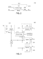
- FIG. 2 illustrates an embodiment of a power circuit with bypass.
- FIG. 3 shows another embodiment of a power circuit.
- FIG. 4 shows an electronic device with a system power architecture according to an embodiment.
- FIGS. 5 and 6 are timing diagrams indicating an embodiment of the sequence of operation of components of an electronic device using a system power architecture according to FIG. 4 for communication systems.
- FIG. 7 illustrates a state table for a power IC according to an embodiment.
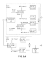
- FIGS. 8A-8B illustrate a corresponding block diagram corresponding to a state diagram for the power IC according to the embodiment of FIG. 7 .
- FIG. 1 illustrates a system power architecture for use in an electronic device according to an embodiment in a block diagram form.
- the electronic device 10 for example, a mobile device such as a smart phone, a tablet computer, a notebook computer, a multimedia player device, and so on.
- the electronic device 10 may be powered by a battery or an external energy source, thus obtaining an input power signal VIN, e.g., a DC signal, and includes a number of electric loads, for example, one or more radio frequency (RF) modules for communication, denoted by RF1, RF2, and RF3, and other system devices, such as system logic 20.
- VIN e.g., a DC signal
- RF1 radio frequency
- RF3 radio frequency
- the electronic device 10 employs a system power architecture including a power integrated circuit (IC) 100 and a power management integrated circuit (PMIC) 200, coupled to the power IC 100.
- the power IC 100 provides appropriate output power signals, e.g., denoted by VOUT1, VOUT2, and VOUT3, for some of the electric loads and the PMIC 200.
- the PMIC 200 receives the output power signal, e.g., VOUT3, from the power IC 100, the PMIC 200 provides other output power signals for the other electronic loads.
- the power IC can be controlled by one or more control signals, e.g., outputted from the system logic 20 or other control source or device, so as to adjust the output power signals with appropriate and sufficient signal levels for driving the electric loads.
- the adjustment to the level of the output power signals may be initiated in view of the status of the energy source, e.g., the energy source in a state of lower or higher output signal level, or in view of the operating mode of the electronic device 10, or in view of power resource control.
- the electronic device 10 is exemplified by a mobile device, such as a smart phone or a tablet computer, with a number of communication systems, e.g., 2G ,3G and LTE, etc., to provide mobile communication functionality.
- the electronic device 10 includes RF modules, such as RF1 or RF2 or RF3, with components for 2G and 3G mobile communications.
- RF1 can be exemplified by a 2G RF module, e.g., including a GSM or a 2G CDMA RF power amplifier.
- RF2 can be exemplified by a 3G RF module, e.g., including a UMTS (such as WCDMA, TD-SCDMA) or CDMA200 RF power amplifier.
- RF3 can be exemplified by a LTE or next generation communication system.
- the power IC 100 includes a number of power converters, e.g., step-up and/or step-down converters, to provide appropriate output power signals for driving the RF modules.
- the power IC 100 may include a first power converter 111, a second power converter 131 for driving the RF modules RF1 and RF2, a third power converter 135 for driving the RF module RF3, and a fourth power converter 115 for providing an output power signal VOUT3 for the PMIC 200.
- Each of the converters selectively operates as a power converter when the input signal does not satisfy an associated threshold and operates in a bypass mode which enables the converter to output its input signal directly as its output signal when the input signal satisfies the associated threshold.
- the first power converter 111 can be a boost converter, denoted by bypass/boost1 in FIG. 1
- the second power converter 113 and third power converter 135 can be buck converters, indicated by bypass/buck1 and bypass/buck2, respectively.
- bypass/boost1 operates as a boost converter to provide an output voltage of a specific level, e.g., 3.1V, 3.3V, 3.5V, or 3.6V.
- the threshold voltage and/or current limit of at least the first power converter 111 can be adjustable and controllable by way of a control signal.
- the first power converter 111 can be set with a different threshold value, in response to a control signal, e.g., via a communication interface such as I2C, SPI, or so on.
- the threshold voltage and/or current limit of other boost or buck with bypass mode can also be controlled in the similar manner. In this way, the power IC 100 can be controlled flexibly or dynamically for providing appropriate output power signals for the electric loads in view of different needs of the mobile device 10.
- bypass/boost1 provides an output power signal VBOUT ⁇ , and bypass/buck1 and bypass/buck2 are coupled to the signal VBOUT ⁇ .
- bypass/boost1 and input terminals of bypass/buck1 and bypass/buck2 are coupled to an energy storage circuit SC, e.g., a capacitor, for energy storage.
- the energy storage circuit SC is charged by the signal VBOUT ⁇ and operates in cooperation with bypass/buck1 and bypass/buck2 in order for bypass/buck1 and bypass/buck2 to provide the output power signals VOUT1 and VOUT2 with appropriate signal levels.
- the output power signal VOUT1 is required for a larger current as indicated above.
- Bypass/buck1 with a larger current limit steps down the signal VBOUT from bypass/boost1 with a lower current limit (e.g., 1.5A) to an adjustable output power signal VOUT1.
- the energy storage circuit SC enables bypass/buck1 to provide a larger current. In this way, the requirement for a larger current for driving the RF module RF1, e.g., including a GSM RF power amplifier, can be fulfilled.
- the energy storage circuit SC e.g., a capacitor, is required to have different capacitance for the requirements for the mobile device which support different communication modes. For example, a mobile device supporting a 2G GSM mode may employ the energy storage circuit SC having a capacitance of about 330uF, and about 10 to 20uF for supporting a CDMA or WCDMA RF Power Amplifier.
- the first power converter 111 can be controllable in different operation mode by way of a control signal denoted by ADJ_BST1.
- ADJ_BST1 can determine if the first power converter 111 has to providing a larger current for driving the RF module 1 mentioned above, e.g., GSM power amplifier. For example, when Vin is lower than a threshold (Vth), ADJ_BST1 can be at a first voltage (e.g., a low level).
- bypass/boost1 111 can operate as a boost converter for outputting a specific output voltage, e.g. 5.5V to provide enough driving capability to bypass/buck1 131 for RF1 module which includes GSM Power Amplifier.
- converter 111 can operate in a bypass mode.
- ADJ_BST1 is at a second voltage (e.g., a high level)
- bypass/boost1 operates as a boost converter or in the bypass mode selectively according to whether the input power signal satisfies the threshold voltage.
- a register (not shown) can be defined in Power IC 100 to reverse the polarity of ADJBST1 by controlling signal, e.g. I2C, to fulfil different RF module requirements for indicating a large current drain request.
- the electronic device 10 can initiate the change of operation mode and/or threshold voltage of the first power converter 111 (or the second power converter 131 and so on) in view of the status of the energy source, such as the energy source in a state of lower or normal output signal level, or in view of the operating mode of the electronic device 10.
- the output power signals such as VOUT1, VOUT2 as well as VBOUT, can be adjustable accordingly for the requirements of the electric loads.
- the following Table provides examples in view of the voltage level of the input power signal VIN, such as the status of an output voltage of a battery unit (such as, high or low battery state), and the communication mode (such as 2G, 3G) in which the electronic device 10 operates.
- ADJ_BST1 can be polarity reserved by I2C control, depending on RF Module design specification) V IN (state) ADJ_BST1 V BOUT Comm. mode V OUT1 Low battery Low 5.5V 2G 3.4V Low battery High Threshold voltage for 3G 3G/4G Depending on the required power High battery Low Bypass Mode ⁇ V IN 2G Bypass Mode ⁇ V BOUT High battery High Bypass Mode ⁇ V IN 3G/4G Depending on the required power
- Control signal ADJ_BST1 can be polarity reserved by I2C control, depending on RF Module design specification.
- ADJ_BST1 when VIN indicates a low battery state, ADJ_BST1 can be set to a low voltage.
- ADJ_BST1 can indicate that bypass/boost1 serves as a boost converter to step up VIN to 5.5V (VBOUT) while Bypass/buck1 is set to provide the output power signal VOUT1 with a fixed voltage of 3.4V.
- VIN satisfies a threshold
- ADJ_BST1 can be low, and converter111 operates in a bypass mode. If VBOUT is higher than VOUT1, converter 131 operates in a buck mode. If VBOUT ⁇ VOUT1, converter 131 operates in the bypass mode.
- ADJ_BST1 is set to a high voltage indicating that bypass/boost1 serves as a boost converter to step up VIN to 3.3V (VBOUT) or enters the bypass mode to output VIN as VBOUT, depending on whether VIN satisfies a threshold voltage for 3G.
- the output power signal VOUT1 of bypass/buck1 depends on the required power for the RF module RF2. In this way, the output voltage of bypass/buck1 can be set dynamically according to the power control of the 3G communication standard, such as power control scheme. For other cases where VIN indicates a high battery state in the Table, one can readily derive the operations following the above discussion.
- the electronic device 10 can further support 4G communication mode, such LTE or LTE-Advanced.
- the third power converter 135 illustrated in FIG. 1 can be used for driving the RF module RF3, e.g. including an RF power amplifier for 4G.
- 3G and 4G modes may be active at the same time and the power IC 100 can be further controlled so that the bypass/buck1 and bypass/buck2 can operate for providing the output power signals VOUT1 and VOUT2 with appropriate signal levels for driving RF modules RF2 and RF3, either individually or both at the same time.
- the bypass/boost1 and bypass/boost2 can be configured with different input current limits, e.g. 2.7A and 1.5A respectively by I2C programming.
- the first power converter 111 and the second power converter 131 can be included in an IC package for driving the RF modules RF1 and RF2.
- the first power converter 111, the second power converter 131, the third power converter 135 can be included in an IC package for driving the RF modules RF1, RF2, and RF3.
- At least one or more power converters of the power IC 100 can be set to a power saving mode, such as on/off or standby or suspend mode, individually by way of a control signal, e.g., denoted by EN_BST1 for bypass/boost1.
- a control signal e.g., denoted by EN_BST1 for bypass/boost1.
- EN_BST1 when EN_BST1 is asserted (i.e., enabled), bypass/boost1 is turned on.
- EN_BK2 is negated (i.e., disabled), bypass/buck2 is turned off.
- the RF module RF3 could be turned off, and bypass/buck2, e.g. converter 135 could be turned off by way of EN_BK2 to reduce power consumption.
- bypass/buck1 and bypass/boost2 can be turned on or off by using EN_BK1 and EN_BST2.
- the power levels for the output power signals of bypass/buck1 and bypass/buck2 can be set by way of analog input signals, e.g., denoted by VCON_BK1 and VCON_BK2, for APT (Auto Power Tracking) or ET (Envelop Tracking).
- VCON_BK1 and VCON_BK2 for APT (Auto Power Tracking) or ET (Envelop Tracking).
- the output power signals can set depending on the duty cycle % of the corresponding VCON_BK1 and VCON_BK2 that are PWM signals.
- bypass/buck1 and bypass/buck2 can be configured to be controlled by way of digital signals, such as the same way as bypass/boost1.
- the fourth power converter 115 can be also included in the power IC 100.
- the fourth power converter 115 e.g., denoted by bypass/boost2, receives the input power signal VIN and provides an output power signal VOUT3 for the PMIC 200.
- the PMIC 200 includes a number of power circuits, such as a first power circuit 210 and a second power circuit 220.
- the first power circuit 210 such as high-voltage low dropout regulators (HV LDO), is used for providing power signals for high-voltage electric loads, such as LCD panel with backlight, camera module, USB module, flash memory, or EMMC memory.
- HV LDO high-voltage low dropout regulators
- the second power circuit 220 such as low-voltage low dropout regulators (LV LDO) and bucks, is used for providing power signals for low-voltage electric loads, such as CPU, SDRAM, DDR memory, control logic, I/O, and other devices.
- the components or IC devices of the electronic device 10 can be regarded as high-voltage and low-voltage electric loads according to the design and requirements of the components or IC devices, and the examples of high-voltage and low-voltage electric loads indicated above are for the sake of explanation only and not limited thereto.
- FIG. 2 illustrates an embodiment of a power circuit with a bypass mode.
- the power circuit 200 such as a boost converter with a bypass mode, includes a bypass circuit 210, control logic 230, and a boost 250.
- the bypass circuit 210 for example, includes at least a switch element 211, such as a transistor switch, controlled by the control logic 230.
- the control logic 230 includes logic circuit or other components and can be controlled for operations as exemplified above for the first power converter 111 or in the examples of the Table.
- the control signal CON for controlling the power converter 200 can be regarded as ADJ_BST1 for setting the power converter 200 in different operation mode.
- control signals e.g., I2C control signal
- control logic 230 detects the input power signal VIN and determines whether VIN satisfies the threshold voltage.
- the power converters of the power IC 100 can be implemented by using the power converter 200.
- FIG. 3 shows another embodiment of a power circuit.
- the power circuit 300 can be configured to replace the power IC 100 as shown in FIG. 1 for the above embodiments.
- the power circuit 300 includes a first power converter 311, a second power converter 331, a third power converter 335, and a fourth power converter 315 for providing an output power signal VOUT3 for the PMIC 200.
- the first power converter 311 receives an input power signal VIN and provides an output power signal VBOUT.
- the second power converter 331 and third power converter 335 provides the outputs power signals VOUT1 and VOUT2.
- the power circuit 300 includes control logic, coupled to the first to fourth power converters, for controlling the first to fourth power converters by way of internal control signals CT1 to CT4.
- each of the power converters includes a bypass circuit (BP).
- BP bypass circuit
- the first power converter 311 includes a bypass circuit BP and a boost circuit (Boost1)
- the second power converter 331 includes a bypass circuit BP and a buck circuit (Buck1).
- the first power converter 311 and the second power converter 331 and the control logic can be included in an IC package.
- the first power converter 311, the second power converter 331, the third power converter 335 can be included in an IC package.
- the fourth power converter 315 can be further included.
- FIG. 4 shows an embodiment of an electronic device with a system power architecture.
- the electronic device 400 for example, a mobile device, such as a smart phone, a tablet computer, a navigation device, a gaming device, or a digital personal assistant and so on, includes a system power unit 410 and a RF unit 420.
- the system power unit 410 employs the system power architecture, as exemplified by the embodiments according to FIGS. 1 to 3 , and includes a power IC 411 and a PMIC 415.
- the power IC 411 and the PMIC 415 receive an input voltage VIN from an energy source, such as a battery unit or an AC-DC adapter or other energy source.
- the power IC 411 provides the output power signals for driving the RF modules of the RF unit 420. Since the power IC 411 can be controlled by setting the threshold voltage and/or current, power control can be performed dynamically and flexibly in view of the communication mode of the electronic device 400.
- the PMIC 415 is used for providing power signals for high-voltage electric loads, such as display unit, camera module, and is used for providing power signals for low-voltage electric loads, such as CPU.
- the electronic device 400 may also include other components, such as DDR memory and flash memory.
- the power IC 411 and the PMIC 415 can be combined as a single chip or the power circuit unit 410 can be configured as a single unit within a chip.
- the system power circuit unit includes a power circuit, in response to a plurality of control signals (such as two or more external control signals as exemplified above) including a first control signal, providing a plurality of output power signals including a first output power signal (e.g., VOUT1) and a second output power signal (V ⁇ OUT2).
- the power circuit includes a plurality of power converters, such as two or more power converters exemplified in FIG. 1 , 2 or 3 , depending on the requirements for the electronic device, such as requirement for powering a radio frequency unit or a functional unit (such as electric loads as exemplified above) or both kinds of units.
- the power circuit includes a first step-up converter, a first step-down converter, and a second step-down converter.
- the first step-up converter (such as 111 or 311), having an input terminal and an output terminal, is coupled to an input power signal (such as VIN) via the input terminal of the first step-up converter.
- the first step-down converter has an input terminal and an output terminal, and the input terminal of the first step-down converter is coupled to the output terminal of the first step-up converter and the output terminal of the first step-down converter for providing the first output power signal.
- the second step-down converter has an input terminal and an output terminal, and the input terminal of the second step-down converter is coupled to the output terminal of the first step-up converter, wherein the input terminals of the first and the second step-down converters are to be coupled to the energy storage circuit.
- Each of the power converters of the power circuit in response to the control signals, selectively operates in one of a plurality of modes including a normal mode and a bypass mode, wherein the normal mode enables the power converter correspondingly stepping up or stepping down an input signal of the power converter when the input signal thereof does not satisfy an associated threshold thereof; and the bypass mode enables the power converter to output the input signal thereof directly as its output signal when the input signal satisfies the associated threshold.
- the power converters of the power circuit further includes a second step-up converter, having an input terminal and an output terminal, the input terminal of the second step-up converter for receiving the input power signal.
- This embodiment further provides an output power signal for use of any purpose.
- system power circuit unit further includes: a power management circuit, coupled to the power circuit, having a plurality of input terminals and a plurality of output terminals, the power management circuit being coupled to the input power signal and the output terminal of the second step-up converter via a first one and a second one of the input terminals of the power management circuit, respectively.
- the power management circuit of this embodiment further utilizes the output power signal from the second step-up converter to provide appropriate voltage for powering of other power consuming electric load.
- one embodiment of the system power the power converters, to control the power converters to operate in one of the modes including the normal mode and the bypass mode, selectively.
- This embodiment adopts an approach to control the power inverters by using a control unit, such as logic circuitry or microcontroller.
- the control unit can be a dedicated circuit embedded in the power circuit (in form of a power IC) or a processing unit such as a CPU of the system or a microcontroller external to the power circuit.
- the power circuit further includes a communication interface (such as I2C, SPI, or so on), the power circuit is coupled to a second control signal of the control signals via the communication interface, wherein in response to the second control signal, the power circuit sets an associated threshold of the step-up converters and step-down converters
- a portable electronic apparatus in general includes a device housing (such as a housing for a smart phone, a tablet computer, an electronic book or any data or media processing device), a display, a processing unit, providing a plurality of control signals for power control, a radio frequency unit, and a system power circuit unit.
- the apparatus can optionally include a holder configured to retain an energy source, such as a battery or any further power source package, for providing the input power signal exemplified above (such as VIN).
- the energy source may have limited energy storage capacity, and when the energy source is going to be drained out, the voltage level provided by the energy source may decrease to a low level which can not satisfy an associated threshold, such as a minimum input voltage required for powering functions of the portable electronic apparatus.
- the system power circuit unit as exemplified above, may include: a power circuit and a power management circuit, coupled to the power circuit.
- the power circuit in response to the control signals and an input power signal, provides a plurality of output power signals for powering the radio frequency unit, the power circuit comprising a plurality of power converters, and provides power signals for powering all or some or a specific one of components or units of the portable electronic apparatus, such as the display and the processing unit in response to the input power signal from the energy source.
- a method for controlling a system power unit may include the following steps.
- the CPU can apply control signal to power IC 411 to set threshold voltage and/or current limit, polarity of ADJ_BST1.
- Power IC 411 can apply power to input of high voltage regulators of PMIC 415 to drive camera module(optional), Flash memory, EMMC memory, or Display with backlight.
- Power IC 411 can also provide output power to drive RF unit 420 while communication is applied.
- the CPU in response to a first communication mode, applies a first control signal to the power IC 411 to change an operation mode of the power converters of the power IC 411 so as to driving a first RF module.
- the CPU in response to a second communication mode, applies a second control signal to the power IC 411 to change the threshold voltage and/or current limit of at least one of the power converters of the power IC 411 so as to driving a second RF module.
- the method can be implemented according to the Table as discussed above.
- a method for powering in a portable electronic device includes the following steps.
- a system power circuit unit is provided, wherein the system power circuit unit includes a power circuit, in response to a plurality of control signals and an input power signal, providing a plurality of output power signals for powering a radio frequency unit of the portable electronic device, the power circuit including a plurality of power converters.
- each of the power converters is selectively enabled in one of a plurality of modes including a normal mode and a bypass mode so as to power a first radio frequency module of the radio frequency unit.
- each of the power converters is selectively enabled in one of the modes so as to power a second radio frequency module of the radio frequency unit.
- the normal mode enables the power converter correspondingly stepping up or stepping down an input signal of the power converter when the input signal thereof does not satisfy an associated threshold thereof; and the bypass mode enables the power converter to output the input signal thereof directly as its output signal when the input signal satisfies the associated threshold.
- an electronic device such as a smart phone, a tablet computer, or any mobile device, supports different communication modes, such as 2G and 3G mode, using a power IC according to the system power architecture as shown in FIG. 4 .
- FIG. 5 is a timing diagram indicating the sequence of operation of components of the electronic device using the power IC according to FIG. 4 in a 2G communication mode.
- an enable signal firstly is asserted when the 2G communication mode (such as a GSM mode) is enabled or a handover is from a 3G mode (such as UMTS) to the GSM mode.
- ADJ_BST1 is enabled (or asserted) for changing the level of the output power signal VBOUT1 of Boost1.
- Boost1 of the power IC 411 outputs an output power signal VBOUT1 of 5.5V (stepping up from 3.3V), for example.
- An enable signal for a buck e.g. EN_BK1 is enabled a period time of T6 before end of T3 to trigger the output of a buck.
- the buck outputs from dynamic to an output level, e.g., 3.4V, within a time interval of T5, in response to the enable signal for the buck.
- an RF PA (such as PA for GSM high band or low band) of the RF unit 420 is enabled.
- the GSM RF PA outputs an output power as required by the requirement for the GSM mode.
- a RF PA for UMTS can be disabled.
- the total time of T1, T2, T3, and T4 is less than 1.3 s, wherein T2+T3, as required by the GSM standard, should be less than 12 ms.
- T1 is set up according to a platform operator while T4 is less than 40 us, for example.
- FIG. 6 is a timing diagram indicating the sequence of operation of components of the mobile device using a power IC according to FIG. 4 in a 3G communication mode.
- an enable signal firstly is asserted when the 3G communication mode (such as a UMTS mode) is enabled or a handover is from a 2G mode (such as a GSM mode) to the UMTS mode.
- a time interval T1 an enable signal ADJBST1 is disabled.
- Boost1 changes its output level, e.g., from 5.5V to 3.3V, for a time interval T2.
- the RF PA for 3G (such as UMTS) is enabled.
- an enable signal for a buck (e.g., EN_BK1) is enabled a time interval T6 before the end of the time period of T3 and the buck outputs from dynamic to an output level for a time interval T5.
- the RF PA for UMTS outputs output power as required.
- the output of the RF PA for 2G (such as GSM) is disabled.
- the total time of T1, T2 is about 1.3 s, and T1 is less than 1ms For example.
- FIG. 7 illustrates a state table for a power IC according to an embodiment.
- the power IC includes four power converters, as embodied by FIG. 1 , 3 , or 4 .
- the power IC can be employed to provide output power signals for driving RF components for different communication modes, such as 2G (such as GSM, CDMA), 3G, or 4G (such as LTE, or so on) mode.
- column "Category” indicates different applications of the power converters for different operation modes and the other columns indicate corresponding conditions or states for those operation modes.
- OUTSU1 and OUTSU2 stands for enabling a first step-up (SU) converter (SU1), such as Boost1 or Bypass/Boost1, as shown in FIG.
- SU1 first step-up converter
- Boost2 or Bypass/Boost2 Boost2 or Bypass/Boost2
- PAEN1 and PAEN2 stands for enabling a first step-down (SD) converter (SD1), such as Buck1 or Bypass/Buck1, as shown in FIG. 1 or 3
- SD1 or Bypass/Buck1 Boost1 or Bypass/Buck1
- SD2 second step-down converter
- SYSEN indicates an enable signal for enabling the power IC, where H indicates enabling while L indicates disabling.
- HV state i.e., the battery voltage or input voltage of SU1 or SU2, denoted by VBAT
- a threshold i.e., the battery voltage or input voltage of SU1 or SU2
- columns “SU1,” “SD1,” “SD2,” and “SU2" represent the levels of the output signals of the power converters, respectively.
- the conditions in parentheses in column “SU1” or “SD2” indicate the criteria for those output levels. For example, for 2G mode in column “Category” with HV (VBAT > Vth of SU1) in column "Battery State,” e.g.
- V_outsu1 is a maximum output level of SU1, which can be set by control signals (such as by way of I2C programming). For the sake of brevity, one of ordinary skill in the art can derive the other operations from FIG. 7 .
- FIGS. 8A-8B illustrate a corresponding block diagram corresponding to a state diagram for the power IC according to the embodiment of FIG. 7 .
- dashed blocks represent the processes (conditions or states (results)) relating to the step-up or step-down converters of a power IC, respectively.
- a process indicated by the dashed block on the upper left side, corresponds to the state diagram for the operation of SU1.
- a first control signal (such as ADJ_BST) is detected so as to determine whether a communication mode is enabled.
- a first mode such as a 2G mode
- a bypass mode is entered and the output signal is substantially the same as the input signal. Otherwise, a boost mode is entered and the output signal is a first value (such as 5.5V).
- a second mode such as a 3G or a CDMA mode
- a second condition such as VBAT > threshold of 3G. If so, a bypass mode is entered and the output signal is substantially the same as the input signal. Otherwise, a boost mode is entered and the output signal is a second value (such as V_outsu1).
- FIGS. 8A-8B thus also provide the embodiments of a method for providing power signals by way of step-up and step-down power conversions.
- the various embodiments of the above show the flexibility of system design according to the system power integrated circuit and architecture.
- the system power circuit unit or the power integrated circuit can be designed or configured to meet various requirements for powering for different purposes.
- the power circuit when the power status of the energy source is under a threshold for operation of one of the components or units, the power circuit performs the step-up conversion of the energy source to provide boosted voltage which is greater than the threshold to prolong the use of time of the energy source. In this way, user experience is enhanced since the battery time for the apparatus can be prolonged.
- Embodiments for a management circuit are provided as follows.
- a management circuit for a portable device includes an input terminal, a first step-up converter, a first step-down converter, and a second step-down converter.
- the input terminal is coupled to receive a supply voltage from a power supply.
- the first step-up converter coupled to the input terminal, selectively converts the supply voltage to a boosted voltage.
- the first step-down converter coupled to the first step-up converter, selectively provides a first output power voltage to a first radio frequency (RF) module (such as a module for 2G, 3G, or 4G).
- the second step-down converter coupled to the first step-up converter, selectively provides a second output power voltage to a second radio frequency (RF) module (such as a module for 2G, 3G, or 4G).
- the first step-up converter performs the conversion of the supply voltage when the supply voltage is under a threshold voltage.
- the first step down converter further includes a storage capacitor and the storage capacitor is pre-charged by the first step-up converter to provide a current for the first step-down converter.
- the boosted voltage is higher or closed to the corresponding threshold voltage.
- the management circuit can further include a processing unit, wherein the processing unit determines the threshold voltage based on operation status of the first and second RF modules. Further, the threshold voltage is a minimum operation voltage for operating one of the first and second RF modules.
- power saving can be implemented in the management circuit in response to the operation of the module to be powered. For example, the first step-down converter is turned off when the first RF module is not used. In another example, the second step-down converter is turned off when the second RF module is not used.
- Embodiments for a power supply arrangement are provided as follows.
- a power supply arrangement for a portable device includes a first input terminal, a first step-up converter, a second step-up converter, a radio frequency unit, and a functional unit.
- the first input terminal is coupled to receive a supply voltage of an energy source.
- the first step-up converter coupled to the first input terminal, selectively converts the supply voltage to a first boosted voltage.
- the second step-up converter coupled to the first input terminal, selectively converts the supply voltage to a second boosted voltage.
- the radio frequency unit (such as a communication module for 2G, 3G, or 4G and so on) has a first operation voltage, coupled to the first step-up converter.
- the functional unit (such as system logic, one or more system components, modules, or sub-units, or any circuitry for performing one or more functions), having a second operation voltage, is coupled to the second step-up converter.
- the first step-up converter performs the conversion of the supply voltage when the supply voltage is lower than the first operation voltage
- the second step-up converter performs the conversion of the supply voltage when the supply voltage is lower than the second operation voltage.
- the above power supply arrangement can further include a processing unit, coupled to the radio frequency unit and the functional unit.
- the processing unit can be configured to: detect the supply voltage; instruct the first step-up converter to perform the conversion of the supply voltage into the first boosted voltage when the supply voltage is lower than the first operation voltage; and instruct the second step-up converter to perform the conversion of the supply voltage into the second boosted voltage when the supply voltage is lower than the second operation voltage.
- the power supply arrangement can further include a step-down converter, coupled to the first step-up converter, for selectively providing an output voltage to the radio frequency unit as the first operation voltage.
- the first embodiment of the power supply arrangement can further include a power management circuit, which has a third input terminal coupled to the second step-up converter and a high voltage output terminal coupled to the functional unit.
- the power management circuit coupled to the second step-up converter, selectively provides a high output voltage to the functional unit as the second operation voltage.
- the functional unit includes: a high voltage electric load (such as an LCD panel with backlight, camera module, USB module, flash memory, or EMMC memory) with the second operation voltage and a low voltage electric load (such as CPU, SDRAM, DDR memory, control logic, I/O, and other devices) with a third operation voltage.
- the power supply arrangement can further include a power management circuit (such as one as an integrated circuit or a portion of circuitry), which has a third input terminal coupled to the second step-up converter and a high voltage output terminal coupled to the high voltage electric load.
- the power management circuit according to the second boosted voltage from the second step-up converter, selectively provides a high output voltage to the high voltage electric load as the second operation voltage.
- the power management circuit can further include a second input terminal coupled to the energy source and a low voltage output terminal coupled to the low voltage electric load.
- the power management circuit according to the energy source, selectively provides a low output voltage to the low voltage electric load as the third operation voltage.
- a power integrated circuit and a power management circuit are connected and the power integrated circuit facilitates the operation of a high voltage electric load through the power management circuit even if the supply voltage is lower than the operation voltage of that load.
- the power supply arrangement includes: a power integrated circuit, a radio frequency unit, a functional unit, and a power management circuit.
- the power integrated circuit with a first input terminal coupled to an energy source, a first output terminal, and a second output terminal, selectively converts a supply voltage of the energy source to a first boosted voltage and selectively converts the supply voltage to a second boosted voltage.
- the radio frequency unit with a first operation voltage, coupled to the first output terminal, receives the first boosted voltage.
- the functional unit includes a high voltage electric load with a second operation voltage; and a low voltage electric load with a third operation voltage.
- the power management circuit includes a second input terminal coupled to the energy source; a third input terminal coupled to the second output terminal of the power integrated circuit to receive the second boosted voltage; a third output terminal coupled to the high voltage electric load; and a fourth output terminal coupled to the low voltage electric load.
- the power integrated circuit performs the conversion of the supply voltage when the supply voltage is lower than the second operation voltage, and the power management circuit provide a low output voltage from the energy source to the low voltage electric load as the third operation voltage through the fourth output terminal.
- the power management circuit includes a high voltage low-dropout (LDO) regulator and a low voltage low-dropout (LDO) regulator.
- the high voltage LDO regulator with a first terminal coupled to the second output terminal and a second terminal coupled to the third output terminal, regulates the second boosted voltage to provide a high output voltage as the second operation voltage.
- the low voltage LDO regulator with a first terminal coupled to the second input terminal and a second terminal coupled to the fourth output terminal, regulates the supply voltage to provide the low output voltage as the third operation voltage.
- Embodiments for a portable apparatus are provided as follows.
- a first embodiment of a portable apparatus includes a housing, a power integrated circuit, a radio frequency unit, and a functional unit.
- the power integrated circuit retained in the housing, includes a first input terminal, a first boost converter, and a second boost converter.
- the first input terminal is coupled to an energy source providing a supply voltage.
- the first boost converter with a first terminal coupled to the first input terminal and a second terminal, selectively converts the supply voltage to a first boosted voltage through the second terminal of the first boost converter.
- the second boost converter with a first terminal coupled to the first input terminal and a second terminal, selectively converts the supply voltage to a second boosted voltage through the second terminal of the second boost converter.
- the radio frequency unit with a first operation voltage, is retained in the housing and coupled to the first boost converter.
- the functional unit with a second operation voltage, is retained in the housing and coupled to the second boost converter.
- the first boost converter performs the conversion of the supply voltage when the supply voltage is lower than the first operation voltage
- the second boost converter performs the conversion of the supply voltage when the supply voltage is lower than the second operation voltage.
- the above portable apparatus can further include a processing unit, coupled to the radio frequency unit and the functional unit.
- the processing unit can be configured to: detect the supply voltage; instruct the first boost converter to perform the conversion of the supply voltage into the first boosted voltage when the supply voltage is lower than the first operation voltage; and instruct the second boost converter to perform the conversion of the supply voltage into the second boosted voltage when the supply voltage is lower than the second operation voltage.
- the first embodiment of the portable apparatus can further include a power management circuit, which has an input terminal coupled to the second terminal of the second boost converter and a high voltage output terminal coupled to the functional unit.
- the power management circuit selectively provides a high output voltage from the second boost converter to the functional unit as the second operation voltage.
- a second embodiment of the portable apparatus includes a housing, a power integrated circuit, a radio frequency unit, and a functional unit.
- the power integrated circuit retained in the housing, includes a first input terminal, a first boost converter, and a second boost converter.
- the first input terminal is coupled to an energy source providing a supply voltage.
- the first boost converter with a first terminal coupled to the first input terminal and a second terminal, selectively boosts the supply voltage to an output voltage through the second terminal of the first boost converter.
- the second boost converter with a first terminal coupled to the first input terminal and a second terminal, selectively boosts the supply voltage to a high output voltage through the second terminal of the second boost converter.
- the radio frequency unit with a first operation voltage, is retained in the housing and coupled to the second terminal of the first boost converter.
- the first boost converter performs the conversion of the supply voltage when the supply voltage is lower than the first operation voltage
- the second boost converter performs the conversion of the supply voltage when the supply voltage is lower than the second operation voltage.
- the second embodiment of the portable apparatus can further include a processing unit, coupled to the radio frequency unit and the functional unit.
- the processing unit can be configured to: detect the supply voltage; instruct the first boost converter to perform the conversion of the supply voltage into the output voltage of the first boost converter when the supply voltage is lower than the first operation voltage; and instruct the second boost converter to perform the conversion of the supply voltage into the high output voltage when the supply voltage is lower than the second operation voltage.
- the power integrated circuit can further be configured to provide the output voltage of the first boost converter to the radio frequency unit as the first operation voltage.
- the second embodiment of the portable apparatus can further include a power management circuit, which is retained in the housing and has a third input terminal coupled to the second boost converter and a high voltage output terminal coupled to the high voltage electric load.
- the power management circuit selectively provides the high output voltage from the second boost converter to the high voltage electric load as the second operation voltage.
- the power management circuit can further include a second input terminal coupled to the energy source and a low voltage output terminal coupled to the low voltage electric load, and selectively provides a low output voltage from the energy source to the low voltage electric load as the third operation voltage.
- a third embodiment of the portable apparatus includes a housing, a power integrated circuit, a radio frequency unit, a functional unit, and a power management circuit.
- the power integrated circuit is retained in the housing, with a first input terminal coupled to an energy source, a first output terminal, and a second output terminal.
- the power integrated circuit selectively converts a supply voltage of the energy source to a first boosted voltage and for selectively converting the supply voltage to a second boosted voltage.
- the radio frequency unit with a first operation voltage, is retained in the housing and coupled to the first output terminal to receive the first boosted voltage.
- the functional unit includes: a high voltage electric load with a second operation voltage; and a low voltage electric load with a third operation voltage.
- the power management circuit retained in the housing, includes: a second input terminal coupled to the energy source; a third input terminal coupled to the second output terminal of the power integrated circuit to receive the second boosted voltage; a third output terminal coupled to the high voltage electric load; and a fourth output terminal coupled to the low voltage electric load.
- the power integrated circuit performs the conversion of the supply voltage when the supply voltage is lower than the second operation voltage, and the power management circuit provides a low output voltage from the energy source to the low voltage electric load as the third operation voltage through the fourth output terminal.
- the power management circuit can further include: a high voltage low-dropout regulator and a low voltage low-dropout regulator.
- the high voltage low-dropout regulator with a first terminal coupled to the second output terminal of the power integrated circuit and a second terminal coupled to the fourth output terminal, regulates the second boosted voltage to provide a high output voltage as the second operation voltage.
- the low voltage low-dropout regulator with a first terminal coupled to the second input terminal and a second terminal coupled to the fourth output terminal, regulates the supply voltage to provide the low output voltage as the third operation voltage.
- the above embodiments disclose a system power integrated circuit and system power architecture for portable devices and a method for controlling the same, and a method for providing power signals.
- Power control can be performed dynamically and flexibly in view of the status of the energy source, e.g., the energy source in a state of lower or higher output signal level, or in view of the operating mode of the electronic device, or in view of power resource control.
- the energy source in a low power state can still provide appropriate power signals for driving the RF module by way of the power converters and the energy storage circuit.
Abstract
Description
- The disclosure relates in general to power integrated circuit, and more particularly to a system power integrated circuit and system power architecture for portable devices, management circuit, power supply arrangement, and portable apparatus.
- Mobile devices, such as a smart phone or a tablet computer, now become indispensable to many people. The mobile devices are very versatility but the use of their functionality may lead to a large amount of power consumption and energy capacity of the energy source, e.g. battery, for powering the devices is very limited. In particular, the mobile devices include telecommunication modules such as 2G, 3G, or 4G, that are very energy consuming and sensitive to the power level of the energy source. As such, power control and management in the mobile devices become critical.
- The disclosure is directed to a system power integrated circuit and system power architecture for portable devices, a method for controlling the same and a method for providing power signals. It an object of the present invention to provide a power supply arrangement for a portable device and a method for powering a portable electronic device. This object can be achieved by the features of the independent claims. Further enhancements are characterized by the dependent claims.
- According to an embodiment the present disclosure, a system power architecture for use in an electronic device is provided. The system power architecture includes a power integrated circuit (IC) and a power management integrated circuit (PMIC) coupled to the power IC.
- According to an embodiment the present disclosure, a power integrated circuit is provided. The power integrated circuit includes a number of power converters, wherein each power converter offers a bypass mode and can be controlled.
- According to an embodiment, a power integrated circuit is provided. The power integrated circuit includes a number of power converters and control logic, wherein each power converter offers a bypass mode.
- According to an embodiment, an electronic device with a system power architecture is provided. According to an embodiment, a method for control a system power unit is provided. According to an embodiment, a method for providing power signals is provided.
- According to one embodiment, a management circuit for a portable device includes an input terminal, a first step-up converter, a first step-down converter, and a second step-down converter. The input terminal is coupled to receive a supply voltage from a power supply. The first step-up converter, coupled to the input terminal, selectively converts the supply voltage to a boosted voltage. The first step-down converter, coupled to the first step-up converter, selectively provides a first output power voltage to a first radio frequency (RF) module. The second step-down converter, coupled to the first step-up converter, selectively provides a second output power voltage to a second radio frequency (RF) module. The first step-up converter performs the conversion of the supply voltage when the supply voltage is under a threshold voltage.
- According to one embodiment, a power supply arrangement for a portable device includes a first input terminal, a first step-up converter, a second step-up converter, a radio frequency unit, and a functional unit. The first input terminal is coupled to receive a supply voltage of an energy source. The first step-up converter, coupled to the first input terminal, selectively converts the supply voltage to a first boosted voltage. The second step-up converter, coupled to the first input terminal, selectively converts the supply voltage to a second boosted voltage. The radio frequency unit (such as a communication module for 2G, 3G, or 4G and so on) has a first operation voltage, coupled to the first step-up converter. The functional unit (such as system logic, one or more system components, modules, or sub-units, or any circuitry for performing one or more functions), having a second operation voltage, is coupled to the second step-up converter. The first step-up converter performs the conversion of the supply voltage when the supply voltage is lower than the first operation voltage, and the second step-up converter performs the conversion of the supply voltage when the supply voltage is lower than the second operation voltage.
- According to another embodiment, a power supply arrangement includes: a power integrated circuit, a radio frequency unit, a functional unit, and a power management circuit. The power integrated circuit, with a first input terminal coupled to an energy source, a first output terminal, and a second output terminal, selectively converts a supply voltage of the energy source to a first boosted voltage and selectively converts the supply voltage to a second boosted voltage. The radio frequency unit with a first operation voltage, coupled to the first output terminal, receives the first boosted voltage. The functional unit includes a high voltage electric load with a second operation voltage; and a low voltage electric load with a third operation voltage. The power management circuit includes a second input terminal coupled to the energy source; a third input terminal coupled to the second output terminal of the power integrated circuit to receive the second boosted voltage; a third output terminal coupled to the high voltage electric load; and a fourth output terminal coupled to the low voltage electric load. The power integrated circuit performs the conversion of the supply voltage when the supply voltage is lower than the second operation voltage, and the power management circuit provide a low output voltage from the energy source to the low voltage electric load as the third operation voltage through the fourth output terminal.
- According to an embodiment, a portable apparatus includes a housing, a power integrated circuit, a radio frequency unit, and a functional unit. The power integrated circuit, retained in the housing, includes a first input terminal, a first boost converter, and a second boost converter. The first input terminal is coupled to an energy source providing a supply voltage. The first boost converter, with a first terminal coupled to the first input terminal and a second terminal, selectively converts the supply voltage to a first boosted voltage through the second terminal of the first boost converter. The second boost converter, with a first terminal coupled to the first input terminal and a second terminal, selectively converts the supply voltage to a second boosted voltage through the second terminal of the second boost converter. The radio frequency unit, with a first operation voltage, is retained in the housing and coupled to the first boost converter. The functional unit, with a second operation voltage, is retained in the housing and coupled to the second boost converter. The first boost converter performs the conversion of the supply voltage when the supply voltage is lower than the first operation voltage, and the second boost converter performs the conversion of the supply voltage when the supply voltage is lower than the second operation voltage.
- According to another embodiment, a portable apparatus includes a housing, a power integrated circuit, a radio frequency unit, and a functional unit. The power integrated circuit, retained in the housing, includes a first input terminal, a first boost converter, and a second boost converter. The first input terminal is coupled to an energy source providing a supply voltage. The first boost converter, with a first terminal coupled to the first input terminal and a second terminal, selectively boosts the supply voltage to an output voltage through the second terminal of the first boost converter. The second boost converter, with a first terminal coupled to the first input terminal and a second terminal, selectively boosts the supply voltage to a high output voltage through the second terminal of the second boost converter. The radio frequency unit, with a first operation voltage, is retained in the housing and coupled to the second terminal of the first boost converter. The functional unit, retained in the housing and coupled to the second terminal of the second boost converter, includes a high voltage electric load with a second operation voltage and a low voltage electric load with a third operation voltage. The first boost converter performs the conversion of the supply voltage when the supply voltage is lower than the first operation voltage, and the second boost converter performs the conversion of the supply voltage when the supply voltage is lower than the second operation voltage.
- According to still another embodiment, a portable apparatus includes a housing, a power integrated circuit, a radio frequency unit, a functional unit, and a power management circuit. The power integrated circuit is retained in the housing, with a first input terminal coupled to an energy source, a first output terminal, and a second output terminal. The power integrated circuit selectively converts a supply voltage of the energy source to a first boosted voltage and for selectively converting the supply voltage to a second boosted voltage. The radio frequency unit, with a first operation voltage, is retained in the housing and coupled to the first output terminal to receive the first boosted voltage. The functional unit includes: a high voltage electric load with a second operation voltage, and a low voltage electric load with a third operation voltage. The power management circuit, retained in the housing, includes: a second input terminal coupled to the energy source; a third input terminal coupled to the second output terminal of the power integrated circuit to receive the second boosted voltage; a third output terminal coupled to the high voltage electric load; and a fourth output terminal coupled to the low voltage electric load. The power integrated circuit performs the conversion of the supply voltage when the supply voltage is lower than the second operation voltage, and the power management circuit provide a low output voltage from the energy source to the low voltage electric load as the third operation voltage through the fourth output terminal.
- According to one embodiment, a system power circuit unit includes a power circuit, in response to a plurality of control signals including a first control signal, providing a plurality of output power signals including a first output power signal and a second output power signal. The power circuit includes a plurality of power converters. For example, the power circuit includes a first step-up converter, a first step-down converter, and a second step-down converter. The first step-up converter, having an input terminal and an output terminal, is coupled to an input power signal via the input terminal of the first step-up converter. The first step-down converter has an input terminal and an output terminal, and the input terminal of the first step-down converter is coupled to the output terminal of the first step-up converter and the output terminal of the first step-down converter for providing the first output power signal. The second step-down converter has an input terminal and an output terminal, and the input terminal of the second step-down converter is coupled to the output terminal of the first step-up converter, wherein the input terminals of the first and the second step-down converters are to be coupled to the energy storage circuit. Each of the power converters of the power circuit, in response to the control signals, selectively operates in one of a plurality of modes including a normal mode and a bypass mode, wherein the normal mode enables the power converter correspondingly stepping up or stepping down an input signal of the power converter when the input signal thereof does not satisfy an associated threshold thereof; and the bypass mode enables the power converter to output the input signal thereof directly as its output signal when the input signal satisfies the associated threshold.
- According to an embodiment of a portable apparatus in general is provided associated with the system power circuit unit as exemplified above. In such embodiment, a portable electronic apparatus includes a device housing (such as a housing for a smart phone, a tablet computer, an electronic book or any data or media processing device), a display, a processing unit, providing a plurality of control signals for power control, a radio frequency unit, and a system power circuit unit. The apparatus can optionally include a holder configured to retain an energy source, such as a battery or any further power source package. The system power circuit unit as exemplified above, may include: a power circuit and a power management circuit, coupled to the power circuit. The power circuit, in response to the control signals and an input power signal, provides a plurality of output power signals for powering the radio frequency unit, the power circuit comprising a plurality of power converters, and provides power signals for powering all or some or a specific one of components or units of the portable electronic apparatus, such as the display and the processing unit in response to the input power signal from the energy source.
- According to an embodiment, a method for powering in a portable electronic device, includes the following steps. A system power circuit unit is provided, wherein the system power circuit unit comprises a power circuit, in response to a plurality of control signals and an input power signal, providing a plurality of output power signals for powering a radio frequency unit of the portable electronic device, the power circuit comprising a plurality of power converters. In response to a first control signal indicating a first communication mode for the portable electronic device, each of the power converters is selectively enabled in one of a plurality of modes including a normal mode and a bypass mode so as to power a first radio frequency module of the radio frequency unit. In response to the first control signal indicating a second communication mode for the portable electronic device, each of the power converters is selectively enabled in one of the modes so as to power a second radio frequency module of the radio frequency unit. The normal mode enables the power converter correspondingly stepping up or stepping down an input signal of the power converter when the input signal thereof does not satisfy an associated threshold thereof; and the bypass mode enables the power converter to output the input signal thereof directly as its output signal when the input signal satisfies the associated threshold.
- The above and other aspects of the disclosure will become better understood with regard to the following detailed description of the non-limiting embodiment(s). The following description is made with reference to the accompanying drawings.
-
FIG. 1 illustrates a system power architecture for use in an electronic device according to an embodiment in a block diagram. -
FIG. 2 illustrates an embodiment of a power circuit with bypass. -
FIG. 3 shows another embodiment of a power circuit. -
FIG. 4 shows an electronic device with a system power architecture according to an embodiment. -
FIGS. 5 and6 are timing diagrams indicating an embodiment of the sequence of operation of components of an electronic device using a system power architecture according toFIG. 4 for communication systems. -
FIG. 7 illustrates a state table for a power IC according to an embodiment. -
FIGS. 8A-8B illustrate a corresponding block diagram corresponding to a state diagram for the power IC according to the embodiment ofFIG. 7 . -
FIG. 1 illustrates a system power architecture for use in an electronic device according to an embodiment in a block diagram form. Theelectronic device 10, for example, a mobile device such as a smart phone, a tablet computer, a notebook computer, a multimedia player device, and so on. Theelectronic device 10 may be powered by a battery or an external energy source, thus obtaining an input power signal VIN, e.g., a DC signal, and includes a number of electric loads, for example, one or more radio frequency (RF) modules for communication, denoted by RF1, RF2, and RF3, and other system devices, such assystem logic 20. - According to the embodiment, the
electronic device 10 employs a system power architecture including a power integrated circuit (IC) 100 and a power management integrated circuit (PMIC) 200, coupled to thepower IC 100. In response to the VIN, thepower IC 100 provides appropriate output power signals, e.g., denoted by VOUT1, VOUT2, and VOUT3, for some of the electric loads and thePMIC 200. Receiving the output power signal, e.g., VOUT3, from thepower IC 100, thePMIC 200 provides other output power signals for the other electronic loads. In particular, the power IC can be controlled by one or more control signals, e.g., outputted from thesystem logic 20 or other control source or device, so as to adjust the output power signals with appropriate and sufficient signal levels for driving the electric loads. For example, the adjustment to the level of the output power signals may be initiated in view of the status of the energy source, e.g., the energy source in a state of lower or higher output signal level, or in view of the operating mode of theelectronic device 10, or in view of power resource control. - In one embodiment, the
electronic device 10 is exemplified by a mobile device, such as a smart phone or a tablet computer, with a number of communication systems, e.g., 2G ,3G and LTE, etc., to provide mobile communication functionality. Following this embodiment, theelectronic device 10 includes RF modules, such as RF1 or RF2 or RF3, with components for 2G and 3G mobile communications. For example, RF1 can be exemplified by a 2G RF module, e.g., including a GSM or a 2G CDMA RF power amplifier. RF2 can be exemplified by a 3G RF module, e.g., including a UMTS (such as WCDMA, TD-SCDMA) or CDMA200 RF power amplifier. RF3 can be exemplified by a LTE or next generation communication system. - In the above embodiment, the
power IC 100 includes a number of power converters, e.g., step-up and/or step-down converters, to provide appropriate output power signals for driving the RF modules. As exemplified inFIG. 1 , thepower IC 100 may include a first power converter 111, asecond power converter 131 for driving the RF modules RF1 and RF2, athird power converter 135 for driving the RF module RF3, and afourth power converter 115 for providing an output power signal VOUT3 for thePMIC 200. Each of the converters selectively operates as a power converter when the input signal does not satisfy an associated threshold and operates in a bypass mode which enables the converter to output its input signal directly as its output signal when the input signal satisfies the associated threshold. For example, the first power converter 111 can be a boost converter, denoted by bypass/boost1 inFIG. 1 , while the second power converter 113 andthird power converter 135 can be buck converters, indicated by bypass/buck1 and bypass/buck2, respectively. For bypass/boost1 with a threshold voltage of 3.3V, when VIN >= 3.3V, bypass/boost1 operates in the bypass mode. When VIN < 3.3V, bypass/boost1 operates as a boost converter to provide an output voltage of a specific level, e.g., 3.1V, 3.3V, 3.5V, or 3.6V. - In particular, the threshold voltage and/or current limit of at least the first power converter 111 can be adjustable and controllable by way of a control signal. For example, the first power converter 111 can be set with a different threshold value, in response to a control signal, e.g., via a communication interface such as I2C, SPI, or so on. In other examples, the threshold voltage and/or current limit of other boost or buck with bypass mode can also be controlled in the similar manner. In this way, the
power IC 100 can be controlled flexibly or dynamically for providing appropriate output power signals for the electric loads in view of different needs of themobile device 10. - In the embodiment of the
electronic device 10 as a mobile device, 2G and 3G modes would not be active at the same time. When theelectronic device 10 is in a 2G mode, the RF1 requires a larger driving current of 2.5A, for example. In this case, the threshold (Vth) of bypass/boost1 is set to a higher value, e.g., 3.5V or 3.6V. In a 3G mode, the RF2 requires a lower power consumption and a lower driving current of about 560 to 800mA, Vth is set to a lower value, e.g., 3.3V. Bypass/boost1 provides an output power signal VBOUT¬¬¬, and bypass/buck1 and bypass/buck2 are coupled to the signal VBOUT¬¬¬. In addition, the output terminal of bypass/boost1 and input terminals of bypass/buck1 and bypass/buck2 are coupled to an energy storage circuit SC, e.g., a capacitor, for energy storage. The energy storage circuit SC is charged by the signal VBOUT¬¬¬ and operates in cooperation with bypass/buck1 and bypass/buck2 in order for bypass/buck1 and bypass/buck2 to provide the output power signals VOUT1 and VOUT2 with appropriate signal levels. For example, in the 2G mode, the output power signal VOUT1 is required for a larger current as indicated above. Bypass/buck1 with a larger current limit (e.g., 2.5A or 2A) steps down the signal VBOUT from bypass/boost1 with a lower current limit (e.g., 1.5A) to an adjustable output power signal VOUT1. The energy storage circuit SC enables bypass/buck1 to provide a larger current. In this way, the requirement for a larger current for driving the RF module RF1, e.g., including a GSM RF power amplifier, can be fulfilled. Further, the energy storage circuit SC, e.g., a capacitor, is required to have different capacitance for the requirements for the mobile device which support different communication modes. For example, a mobile device supporting a 2G GSM mode may employ the energy storage circuit SC having a capacitance of about 330uF, and about 10 to 20uF for supporting a CDMA or WCDMA RF Power Amplifier. - In an embodiment, the first power converter 111 can be controllable in different operation mode by way of a control signal denoted by ADJ_BST1. ADJ_BST1 can determine if the first power converter 111 has to providing a larger current for driving the
RF module 1 mentioned above, e.g., GSM power amplifier. For example, when Vin is lower than a threshold (Vth), ADJ_BST1 can be at a first voltage (e.g., a low level). Correspondingly, bypass/boost1 111 can operate as a boost converter for outputting a specific output voltage, e.g. 5.5V to provide enough driving capability to bypass/buck1 131 for RF1 module which includes GSM Power Amplifier. In contrast, when Vin is higher than Vth, converter 111 can operate in a bypass mode. Correspondingly, ADJ_BST1 is at a second voltage (e.g., a high level), bypass/boost1 operates as a boost converter or in the bypass mode selectively according to whether the input power signal satisfies the threshold voltage. In an embodiment, a register (not shown) can be defined inPower IC 100 to reverse the polarity of ADJBST1 by controlling signal, e.g. I2C, to fulfil different RF module requirements for indicating a large current drain request. - In further embodiments, the
electronic device 10 can initiate the change of operation mode and/or threshold voltage of the first power converter 111 (or thesecond power converter 131 and so on) in view of the status of the energy source, such as the energy source in a state of lower or normal output signal level, or in view of the operating mode of theelectronic device 10. The output power signals, such as VOUT1, VOUT2 as well as VBOUT, can be adjustable accordingly for the requirements of the electric loads. The following Table provides examples in view of the voltage level of the input power signal VIN, such as the status of an output voltage of a battery unit (such as, high or low battery state), and the communication mode (such as 2G, 3G) in which theelectronic device 10 operates.TABLE (* ADJ_BST1 can be polarity reserved by I2C control, depending on RF Module design specification) VIN (state) ADJ_BST1 VBOUT Comm. mode VOUT1 Low battery Low 5.5 V 2G 3.4V Low battery High Threshold voltage for 3G 3G/4G Depending on the required power High battery Low Bypass Mode ∼ V IN2G Bypass Mode ∼ VBOUT High battery High Bypass Mode ∼ V IN3G/4G Depending on the required power - The above table illustrates the relationship between control signal and output voltage under different RF communication modes. Control signal ADJ_BST1 can be polarity reserved by I2C control, depending on RF Module design specification.
- In 2G mode, when VIN indicates a low battery state, ADJ_BST1 can be set to a low voltage. Correspondingly, ADJ_BST1 can indicate that bypass/boost1 serves as a boost converter to step up VIN to 5.5V (VBOUT) while Bypass/buck1 is set to provide the output power signal VOUT1 with a fixed voltage of 3.4V. On the other hand, when VIN satisfies a threshold, ADJ_BST1 can be low, and converter111 operates in a bypass mode. If VBOUT is higher than VOUT1,
converter 131 operates in a buck mode. If VBOUT < VOUT1,converter 131 operates in the bypass mode. - In another case that the
electronic device 10 operates in 3G/4G mode, when VIN indicates a low battery state, ADJ_BST1 is set to a high voltage indicating that bypass/boost1 serves as a boost converter to step up VIN to 3.3V (VBOUT) or enters the bypass mode to output VIN as VBOUT, depending on whether VIN satisfies a threshold voltage for 3G. In addition, the output power signal VOUT1 of bypass/buck1 depends on the required power for the RF module RF2. In this way, the output voltage of bypass/buck1 can be set dynamically according to the power control of the 3G communication standard, such as power control scheme. For other cases where VIN indicates a high battery state in the Table, one can readily derive the operations following the above discussion. - In other embodiments, the
electronic device 10 can further support 4G communication mode, such LTE or LTE-Advanced. Following these embodiments, thethird power converter 135 illustrated inFIG. 1 can be used for driving the RF module RF3, e.g. including an RF power amplifier for 4G. In these embodiments, 3G and 4G modes may be active at the same time and thepower IC 100 can be further controlled so that the bypass/buck1 and bypass/buck2 can operate for providing the output power signals VOUT1 and VOUT2 with appropriate signal levels for driving RF modules RF2 and RF3, either individually or both at the same time. In an embodiment, the bypass/boost1 and bypass/boost2 can be configured with different input current limits, e.g. 2.7A and 1.5A respectively by I2C programming. - In one embodiment, the first power converter 111 and the
second power converter 131 can be included in an IC package for driving the RF modules RF1 and RF2. In another embodiment, the first power converter 111, thesecond power converter 131, thethird power converter 135 can be included in an IC package for driving the RF modules RF1, RF2, and RF3. - In other embodiment, for system power management, at least one or more power converters of the
power IC 100 according to the above embodiments can be set to a power saving mode, such as on/off or standby or suspend mode, individually by way of a control signal, e.g., denoted by EN_BST1 for bypass/boost1. For example, when EN_BST1 is asserted (i.e., enabled), bypass/boost1 is turned on. In other example, when EN_BK2 is negated (i.e., disabled), bypass/buck2 is turned off. In a situation where only one RF module is used, e.g. 3G is only used, the RF module RF3 could be turned off, and bypass/buck2,e.g. converter 135 could be turned off by way of EN_BK2 to reduce power consumption. Likewise, for bypass/buck1 and bypass/boost2 can be turned on or off by using EN_BK1 and EN_BST2. - In other embodiments, the power levels for the output power signals of bypass/buck1 and bypass/buck2 can be set by way of analog input signals, e.g., denoted by VCON_BK1 and VCON_BK2, for APT (Auto Power Tracking) or ET (Envelop Tracking). For example, the output power signals can set depending on the duty cycle % of the corresponding VCON_BK1 and VCON_BK2 that are PWM signals. In other embodiments, bypass/buck1 and bypass/buck2 can be configured to be controlled by way of digital signals, such as the same way as bypass/boost1.
- In the above embodiments, the
fourth power converter 115 can be also included in thepower IC 100. Thefourth power converter 115, e.g., denoted by bypass/boost2, receives the input power signal VIN and provides an output power signal VOUT3 for thePMIC 200. ThePMIC 200 includes a number of power circuits, such as afirst power circuit 210 and asecond power circuit 220. Thefirst power circuit 210, such as high-voltage low dropout regulators (HV LDO), is used for providing power signals for high-voltage electric loads, such as LCD panel with backlight, camera module, USB module, flash memory, or EMMC memory. Thesecond power circuit 220, such as low-voltage low dropout regulators (LV LDO) and bucks, is used for providing power signals for low-voltage electric loads, such as CPU, SDRAM, DDR memory, control logic, I/O, and other devices. The components or IC devices of theelectronic device 10 can be regarded as high-voltage and low-voltage electric loads according to the design and requirements of the components or IC devices, and the examples of high-voltage and low-voltage electric loads indicated above are for the sake of explanation only and not limited thereto. -
FIG. 2 illustrates an embodiment of a power circuit with a bypass mode. Thepower circuit 200, such as a boost converter with a bypass mode, includes abypass circuit 210,control logic 230, and aboost 250. Thebypass circuit 210, for example, includes at least aswitch element 211, such as a transistor switch, controlled by thecontrol logic 230. Thecontrol logic 230 includes logic circuit or other components and can be controlled for operations as exemplified above for the first power converter 111 or in the examples of the Table. The control signal CON for controlling thepower converter 200 can be regarded as ADJ_BST1 for setting thepower converter 200 in different operation mode. There are control signals, e.g., I2C control signal, (not shown) to communicate withcontrol logic 230 for setting the threshold voltage and/or current limit, as discussed above. When thepower circuit 200 operates as a boost converter or in the bypass mode, thecontrol logic 230 detects the input power signal VIN and determines whether VIN satisfies the threshold voltage. In one embodiment, the power converters of thepower IC 100 can be implemented by using thepower converter 200. -
FIG. 3 shows another embodiment of a power circuit. Thepower circuit 300 can be configured to replace thepower IC 100 as shown inFIG. 1 for the above embodiments. Thepower circuit 300 includes afirst power converter 311, asecond power converter 331, athird power converter 335, and afourth power converter 315 for providing an output power signal VOUT3 for thePMIC 200. Thefirst power converter 311 receives an input power signal VIN and provides an output power signal VBOUT. Thesecond power converter 331 andthird power converter 335 provides the outputs power signals VOUT1 and VOUT2. In addition, thepower circuit 300 includes control logic, coupled to the first to fourth power converters, for controlling the first to fourth power converters by way of internal control signals CT1 to CT4. In addition, the control logic of thepower converter 300 receives external control signals, such as ADJ_BST1, EN_BST1, EN_BST2, EN_BK1, EN_BK2, or I2C or any other form of signals indicating the setting of threshold voltages and/or current limit, tuning on and off of the power converter, or setting the operation mode of the power converter. In addition, each of the power converters includes a bypass circuit (BP). For example, thefirst power converter 311 includes a bypass circuit BP and a boost circuit (Boost1), and thesecond power converter 331 includes a bypass circuit BP and a buck circuit (Buck1). - In one embodiment, the
first power converter 311 and thesecond power converter 331 and the control logic can be included in an IC package. In another embodiment, thefirst power converter 311, thesecond power converter 331, thethird power converter 335 can be included in an IC package. In other embodiments, thefourth power converter 315 can be further included. -
FIG. 4 shows an embodiment of an electronic device with a system power architecture. Theelectronic device 400, for example, a mobile device, such as a smart phone, a tablet computer, a navigation device, a gaming device, or a digital personal assistant and so on, includes asystem power unit 410 and aRF unit 420. Thesystem power unit 410 employs the system power architecture, as exemplified by the embodiments according toFIGS. 1 to 3 , and includes apower IC 411 and aPMIC 415. Thepower IC 411 and thePMIC 415 receive an input voltage VIN from an energy source, such as a battery unit or an AC-DC adapter or other energy source. As exemplified by the above embodiments, thepower IC 411 provides the output power signals for driving the RF modules of theRF unit 420. Since thepower IC 411 can be controlled by setting the threshold voltage and/or current, power control can be performed dynamically and flexibly in view of the communication mode of theelectronic device 400. ThePMIC 415 is used for providing power signals for high-voltage electric loads, such as display unit, camera module, and is used for providing power signals for low-voltage electric loads, such as CPU. Theelectronic device 400 may also include other components, such as DDR memory and flash memory. In other embodiments, thepower IC 411 and thePMIC 415 can be combined as a single chip or thepower circuit unit 410 can be configured as a single unit within a chip. - Other embodiments of a system power circuit unit for use in an electronic device generally are provided as follows.
- In one embodiment, the system power circuit unit includes a power circuit, in response to a plurality of control signals (such as two or more external control signals as exemplified above) including a first control signal, providing a plurality of output power signals including a first output power signal (e.g., VOUT1) and a second output power signal (V¬OUT2). The power circuit includes a plurality of power converters, such as two or more power converters exemplified in
FIG. 1 ,2 or 3 , depending on the requirements for the electronic device, such as requirement for powering a radio frequency unit or a functional unit (such as electric loads as exemplified above) or both kinds of units. For example, the power circuit includes a first step-up converter, a first step-down converter, and a second step-down converter. The first step-up converter (such as 111 or 311), having an input terminal and an output terminal, is coupled to an input power signal (such as VIN) via the input terminal of the first step-up converter. The first step-down converter has an input terminal and an output terminal, and the input terminal of the first step-down converter is coupled to the output terminal of the first step-up converter and the output terminal of the first step-down converter for providing the first output power signal. The second step-down converter has an input terminal and an output terminal, and the input terminal of the second step-down converter is coupled to the output terminal of the first step-up converter, wherein the input terminals of the first and the second step-down converters are to be coupled to the energy storage circuit. Each of the power converters of the power circuit, in response to the control signals, selectively operates in one of a plurality of modes including a normal mode and a bypass mode, wherein the normal mode enables the power converter correspondingly stepping up or stepping down an input signal of the power converter when the input signal thereof does not satisfy an associated threshold thereof; and the bypass mode enables the power converter to output the input signal thereof directly as its output signal when the input signal satisfies the associated threshold. - In another embodiment of the system power circuit unit, the power converters of the power circuit further includes a second step-up converter, having an input terminal and an output terminal, the input terminal of the second step-up converter for receiving the input power signal. This embodiment further provides an output power signal for use of any purpose.
- In another embodiment of the system power circuit unit further includes: a power management circuit, coupled to the power circuit, having a plurality of input terminals and a plurality of output terminals, the power management circuit being coupled to the input power signal and the output terminal of the second step-up converter via a first one and a second one of the input terminals of the power management circuit, respectively. The power management circuit of this embodiment further utilizes the output power signal from the second step-up converter to provide appropriate voltage for powering of other power consuming electric load.
- As exemplified in
FIG. 3 , one embodiment of the system power the power converters, to control the power converters to operate in one of the modes including the normal mode and the bypass mode, selectively. This embodiment adopts an approach to control the power inverters by using a control unit, such as logic circuitry or microcontroller. The control unit can be a dedicated circuit embedded in the power circuit (in form of a power IC) or a processing unit such as a CPU of the system or a microcontroller external to the power circuit. - In one embodiment of the system power circuit unit, the power circuit further includes a communication interface (such as I2C, SPI, or so on), the power circuit is coupled to a second control signal of the control signals via the communication interface, wherein in response to the second control signal, the power circuit sets an associated threshold of the step-up converters and step-down converters
- Further embodiments of a portable electronic apparatus in general are provided as follows in associated with the system power circuit unit as exemplified above. In such embodiments, a portable electronic apparatus includes a device housing (such as a housing for a smart phone, a tablet computer, an electronic book or any data or media processing device), a display, a processing unit, providing a plurality of control signals for power control, a radio frequency unit, and a system power circuit unit. The apparatus can optionally include a holder configured to retain an energy source, such as a battery or any further power source package, for providing the input power signal exemplified above (such as VIN). The energy source may have limited energy storage capacity, and when the energy source is going to be drained out, the voltage level provided by the energy source may decrease to a low level which can not satisfy an associated threshold, such as a minimum input voltage required for powering functions of the portable electronic apparatus. The system power circuit unit as exemplified above, may include: a power circuit and a power management circuit, coupled to the power circuit. The power circuit, in response to the control signals and an input power signal, provides a plurality of output power signals for powering the radio frequency unit, the power circuit comprising a plurality of power converters, and provides power signals for powering all or some or a specific one of components or units of the portable electronic apparatus, such as the display and the processing unit in response to the input power signal from the energy source.
- According to an embodiment, a method for controlling a system power unit may include the following steps. In response to powering on the system, the CPU can apply control signal to
power IC 411 to set threshold voltage and/or current limit, polarity ofADJ_BST1. Power IC 411 can apply power to input of high voltage regulators ofPMIC 415 to drive camera module(optional), Flash memory, EMMC memory, or Display with backlight.Power IC 411 can also provide output power to driveRF unit 420 while communication is applied. The CPU, in response to a first communication mode, applies a first control signal to thepower IC 411 to change an operation mode of the power converters of thepower IC 411 so as to driving a first RF module. The CPU, in response to a second communication mode, applies a second control signal to thepower IC 411 to change the threshold voltage and/or current limit of at least one of the power converters of thepower IC 411 so as to driving a second RF module. In other embodiments, the method can be implemented according to the Table as discussed above. - In another embodiment, a method for powering in a portable electronic device, includes the following steps. A system power circuit unit is provided, wherein the system power circuit unit includes a power circuit, in response to a plurality of control signals and an input power signal, providing a plurality of output power signals for powering a radio frequency unit of the portable electronic device, the power circuit including a plurality of power converters. In response to a first control signal indicating a first communication mode for the portable electronic device, each of the power converters is selectively enabled in one of a plurality of modes including a normal mode and a bypass mode so as to power a first radio frequency module of the radio frequency unit. In response to the first control signal indicating a second communication mode for the portable electronic device, each of the power converters is selectively enabled in one of the modes so as to power a second radio frequency module of the radio frequency unit. The normal mode enables the power converter correspondingly stepping up or stepping down an input signal of the power converter when the input signal thereof does not satisfy an associated threshold thereof; and the bypass mode enables the power converter to output the input signal thereof directly as its output signal when the input signal satisfies the associated threshold.
- In a practical embodiment, an electronic device, such as a smart phone, a tablet computer, or any mobile device, supports different communication modes, such as 2G and 3G mode, using a power IC according to the system power architecture as shown in
FIG. 4 .FIG. 5 is a timing diagram indicating the sequence of operation of components of the electronic device using the power IC according toFIG. 4 in a 2G communication mode. As shown inFIG. 5 , an enable signal firstly is asserted when the 2G communication mode (such as a GSM mode) is enabled or a handover is from a 3G mode (such as UMTS) to the GSM mode. After a time interval T1, ADJ_BST1 is enabled (or asserted) for changing the level of the output power signal VBOUT1 of Boost1. After a time interval T2, Boost1 of thepower IC 411 outputs an output power signal VBOUT1 of 5.5V (stepping up from 3.3V), for example. An enable signal for a buck (e.g. EN_BK1) is enabled a period time of T6 before end of T3 to trigger the output of a buck. As illustrated inFIG. 5 , the buck outputs from dynamic to an output level, e.g., 3.4V, within a time interval of T5, in response to the enable signal for the buck. After a time interval T3, an RF PA (such as PA for GSM high band or low band) of theRF unit 420 is enabled. After a time interval T4, the GSM RF PA outputs an output power as required by the requirement for the GSM mode. Afterwards, a RF PA for UMTS can be disabled. The total time of T1, T2, T3, and T4 is less than 1.3 s, wherein T2+T3, as required by the GSM standard, should be less than 12 ms. In addition, T1 is set up according to a platform operator while T4 is less than 40 us, for example. -
FIG. 6 is a timing diagram indicating the sequence of operation of components of the mobile device using a power IC according toFIG. 4 in a 3G communication mode. As shown inFIG. 6 , an enable signal firstly is asserted when the 3G communication mode (such as a UMTS mode) is enabled or a handover is from a 2G mode (such as a GSM mode) to the UMTS mode. After a time interval T1, an enable signal ADJBST1 is disabled. In response, Boost1 changes its output level, e.g., from 5.5V to 3.3V, for a time interval T2. After a time interval T3, the RF PA for 3G (such as UMTS) is enabled. During the time period of T3, an enable signal for a buck (e.g., EN_BK1) is enabled a time interval T6 before the end of the time period of T3 and the buck outputs from dynamic to an output level for a time interval T5. After a time interval T4, the RF PA for UMTS outputs output power as required. Afterwards, the output of the RF PA for 2G (such as GSM) is disabled. The total time of T1, T2 is about 1.3 s, and T1 is less than 1ms For example. -
FIG. 7 illustrates a state table for a power IC according to an embodiment. In this embodiment, the power IC includes four power converters, as embodied byFIG. 1 ,3 , or4 . The power IC can be employed to provide output power signals for driving RF components for different communication modes, such as 2G (such as GSM, CDMA), 3G, or 4G (such as LTE, or so on) mode. InFIG. 7 , column "Category" indicates different applications of the power converters for different operation modes and the other columns indicate corresponding conditions or states for those operation modes. In particular, OUTSU1 and OUTSU2 stands for enabling a first step-up (SU) converter (SU1), such as Boost1 or Bypass/Boost1, as shown inFIG. 1 or3 , and a second step-up converter (SU2), such as Boost2 or Bypass/Boost2, as shown inFIG. 1 or3 , while PAEN1 and PAEN2 stands for enabling a first step-down (SD) converter (SD1), such as Buck1 or Bypass/Buck1, as shown inFIG. 1 or3 , and a second step-down converter (SD2), such as Buck2 or Bypass/Buck2, as shown inFIG. 1 or3 . SYSEN indicates an enable signal for enabling the power IC, where H indicates enabling while L indicates disabling. Battery state has a HV state, i.e., the battery voltage or input voltage of SU1 or SU2, denoted by VBAT, is greater than a threshold, and a LV state, i.e., VBAT <= threshold. InFIG. 7 , columns "SU1," "SD1," "SD2," and "SU2" represent the levels of the output signals of the power converters, respectively. In addition, the conditions in parentheses in column "SU1" or "SD2" indicate the criteria for those output levels. For example, for 2G mode in column "Category" with HV (VBAT > Vth of SU1) in column "Battery State," e.g. SU1 is in bypass mode, ADJBST1=L, PAEN1=H, and PAEN2=L, if "V_insd1 > V_outsd1" is satisfied, i.e., it is determined that the input signal of SD1 is greater than a maximum output level of SD1, SD1 is in a buck mode with SD1=V_outsd1, i.e., SD1 outputs the output voltage of V_outsd1. Following this example, if "V_insd1 < V_outsd1" is satisfied, then SD1 is in a bypass mode with SD1=V_insd1, i.e., SD1 outputs the input voltage of V_insd1. - In
FIG. 7 , when it is in a GSM mode (2G), SD1 will not enable APT (auto power tracking) mode and SD1 will be in the bypass mode or outputs V_outsd1. When it is in a UMTS or LTE mode (3G or 4G), SD1 or SD2 will enable APT mode/ET mode and the output voltage level of SD1 or SD2 is controlled by APT or ET (e.g., by way of digital signal or analog signal such as PWM signal or triangular signal). In other examples, V_outsu1 is a maximum output level of SU1, which can be set by control signals (such as by way of I2C programming). For the sake of brevity, one of ordinary skill in the art can derive the other operations fromFIG. 7 . -
FIGS. 8A-8B illustrate a corresponding block diagram corresponding to a state diagram for the power IC according to the embodiment ofFIG. 7 . InFIGS. 8A and8B , dashed blocks represent the processes (conditions or states (results)) relating to the step-up or step-down converters of a power IC, respectively. For example, a process, indicated by the dashed block on the upper left side, corresponds to the state diagram for the operation of SU1. First, a first control signal (such as ADJ_BST) is detected so as to determine whether a communication mode is enabled. If a first mode (such as a 2G mode) is enabled, it is determined whether an input signal (such as VBAT) satisfies a first condition (such as VBAT > threshold of 2G). If so, a bypass mode is entered and the output signal is substantially the same as the input signal. Otherwise, a boost mode is entered and the output signal is a first value (such as 5.5V). If a second mode (such as a 3G or a CDMA mode) is enabled, it is determined whether an input signal (such as VBAT) satisfies a second condition (such as VBAT > threshold of 3G). If so, a bypass mode is entered and the output signal is substantially the same as the input signal. Otherwise, a boost mode is entered and the output signal is a second value (such as V_outsu1). - A corresponding process can be also derived from
FIG. 7 and8A-8B for SD1, SD2, or SU2.FIGS. 8A-8B thus also provide the embodiments of a method for providing power signals by way of step-up and step-down power conversions. - As such, the various embodiments of the above show the flexibility of system design according to the system power integrated circuit and architecture. The system power circuit unit or the power integrated circuit can be designed or configured to meet various requirements for powering for different purposes. In addition, in some embodiments, when the power status of the energy source is under a threshold for operation of one of the components or units, the power circuit performs the step-up conversion of the energy source to provide boosted voltage which is greater than the threshold to prolong the use of time of the energy source. In this way, user experience is enhanced since the battery time for the apparatus can be prolonged.
- The implementation of the system power integrated circuit and architecture are not limited to the above embodiments. The following will present further scenarios or embodiments, such as those in form of a management circuit, a power supply arrangement, or a portable apparatus. For the sake of brevity, the scenarios or embodiments can be supported by way of combinations or modifications of elements exemplified in the embodiments and drawings above as well as equivalents.
- Embodiments for a management circuit are provided as follows.
- In one embodiment, a management circuit for a portable device includes an input terminal, a first step-up converter, a first step-down converter, and a second step-down converter. The input terminal is coupled to receive a supply voltage from a power supply. The first step-up converter, coupled to the input terminal, selectively converts the supply voltage to a boosted voltage. The first step-down converter, coupled to the first step-up converter, selectively provides a first output power voltage to a first radio frequency (RF) module (such as a module for 2G, 3G, or 4G). The second step-down converter, coupled to the first step-up converter, selectively provides a second output power voltage to a second radio frequency (RF) module (such as a module for 2G, 3G, or 4G). The first step-up converter performs the conversion of the supply voltage when the supply voltage is under a threshold voltage.
- In another embodiment of the above management circuit, the first step down converter further includes a storage capacitor and the storage capacitor is pre-charged by the first step-up converter to provide a current for the first step-down converter. In addition, the boosted voltage is higher or closed to the corresponding threshold voltage. In another embodiment, the management circuit can further include a processing unit, wherein the processing unit determines the threshold voltage based on operation status of the first and second RF modules. Further, the threshold voltage is a minimum operation voltage for operating one of the first and second RF modules. In some examples, power saving can be implemented in the management circuit in response to the operation of the module to be powered. For example, the first step-down converter is turned off when the first RF module is not used. In another example, the second step-down converter is turned off when the second RF module is not used.
- Embodiments for a power supply arrangement are provided as follows.
- In a first embodiment of the arrangement, a power supply arrangement for a portable device includes a first input terminal, a first step-up converter, a second step-up converter, a radio frequency unit, and a functional unit. The first input terminal is coupled to receive a supply voltage of an energy source. The first step-up converter, coupled to the first input terminal, selectively converts the supply voltage to a first boosted voltage. The second step-up converter, coupled to the first input terminal, selectively converts the supply voltage to a second boosted voltage. The radio frequency unit (such as a communication module for 2G, 3G, or 4G and so on) has a first operation voltage, coupled to the first step-up converter. The functional unit (such as system logic, one or more system components, modules, or sub-units, or any circuitry for performing one or more functions), having a second operation voltage, is coupled to the second step-up converter. The first step-up converter performs the conversion of the supply voltage when the supply voltage is lower than the first operation voltage, and the second step-up converter performs the conversion of the supply voltage when the supply voltage is lower than the second operation voltage.
- The above power supply arrangement can further include a processing unit, coupled to the radio frequency unit and the functional unit. In this example, the processing unit can be configured to: detect the supply voltage; instruct the first step-up converter to perform the conversion of the supply voltage into the first boosted voltage when the supply voltage is lower than the first operation voltage; and instruct the second step-up converter to perform the conversion of the supply voltage into the second boosted voltage when the supply voltage is lower than the second operation voltage. In another embodiment, the power supply arrangement can further include a step-down converter, coupled to the first step-up converter, for selectively providing an output voltage to the radio frequency unit as the first operation voltage.
- The first embodiment of the power supply arrangement can further include a power management circuit, which has a third input terminal coupled to the second step-up converter and a high voltage output terminal coupled to the functional unit. The power management circuit, coupled to the second step-up converter, selectively provides a high output voltage to the functional unit as the second operation voltage.
- In one practical example, the functional unit includes: a high voltage electric load (such as an LCD panel with backlight, camera module, USB module, flash memory, or EMMC memory) with the second operation voltage and a low voltage electric load (such as CPU, SDRAM, DDR memory, control logic, I/O, and other devices) with a third operation voltage. In addition, the power supply arrangement can further include a power management circuit (such as one as an integrated circuit or a portion of circuitry), which has a third input terminal coupled to the second step-up converter and a high voltage output terminal coupled to the high voltage electric load. The power management circuit, according to the second boosted voltage from the second step-up converter, selectively provides a high output voltage to the high voltage electric load as the second operation voltage. In another implementation of the first embodiment of the power supply arrangement, the power management circuit can further include a second input terminal coupled to the energy source and a low voltage output terminal coupled to the low voltage electric load. The power management circuit, according to the energy source, selectively provides a low output voltage to the low voltage electric load as the third operation voltage. These examples show the flexibility in system design for powering the functional unit with different electric loads and the application of the boosted voltage from the power integrated circuit.
- In a second embodiment of the power supply arrangement, a power integrated circuit and a power management circuit are connected and the power integrated circuit facilitates the operation of a high voltage electric load through the power management circuit even if the supply voltage is lower than the operation voltage of that load. The power supply arrangement includes: a power integrated circuit, a radio frequency unit, a functional unit, and a power management circuit. The power integrated circuit, with a first input terminal coupled to an energy source, a first output terminal, and a second output terminal, selectively converts a supply voltage of the energy source to a first boosted voltage and selectively converts the supply voltage to a second boosted voltage. The radio frequency unit with a first operation voltage, coupled to the first output terminal, receives the first boosted voltage. The functional unit includes a high voltage electric load with a second operation voltage; and a low voltage electric load with a third operation voltage. The power management circuit includes a second input terminal coupled to the energy source; a third input terminal coupled to the second output terminal of the power integrated circuit to receive the second boosted voltage; a third output terminal coupled to the high voltage electric load; and a fourth output terminal coupled to the low voltage electric load. The power integrated circuit performs the conversion of the supply voltage when the supply voltage is lower than the second operation voltage, and the power management circuit provide a low output voltage from the energy source to the low voltage electric load as the third operation voltage through the fourth output terminal.
- In an example, the power management circuit includes a high voltage low-dropout (LDO) regulator and a low voltage low-dropout (LDO) regulator. The high voltage LDO regulator, with a first terminal coupled to the second output terminal and a second terminal coupled to the third output terminal, regulates the second boosted voltage to provide a high output voltage as the second operation voltage. The low voltage LDO regulator, with a first terminal coupled to the second input terminal and a second terminal coupled to the fourth output terminal, regulates the supply voltage to provide the low output voltage as the third operation voltage.
- Embodiments for a portable apparatus are provided as follows.
- A first embodiment of a portable apparatus includes a housing, a power integrated circuit, a radio frequency unit, and a functional unit. The power integrated circuit, retained in the housing, includes a first input terminal, a first boost converter, and a second boost converter. The first input terminal is coupled to an energy source providing a supply voltage. The first boost converter, with a first terminal coupled to the first input terminal and a second terminal, selectively converts the supply voltage to a first boosted voltage through the second terminal of the first boost converter. The second boost converter, with a first terminal coupled to the first input terminal and a second terminal, selectively converts the supply voltage to a second boosted voltage through the second terminal of the second boost converter. The radio frequency unit, with a first operation voltage, is retained in the housing and coupled to the first boost converter. The functional unit, with a second operation voltage, is retained in the housing and coupled to the second boost converter. The first boost converter performs the conversion of the supply voltage when the supply voltage is lower than the first operation voltage, and the second boost converter performs the conversion of the supply voltage when the supply voltage is lower than the second operation voltage.
- The above portable apparatus can further include a processing unit, coupled to the radio frequency unit and the functional unit. The processing unit can be configured to: detect the supply voltage; instruct the first boost converter to perform the conversion of the supply voltage into the first boosted voltage when the supply voltage is lower than the first operation voltage; and instruct the second boost converter to perform the conversion of the supply voltage into the second boosted voltage when the supply voltage is lower than the second operation voltage.
- The first embodiment of the portable apparatus can further include a power management circuit, which has an input terminal coupled to the second terminal of the second boost converter and a high voltage output terminal coupled to the functional unit. The power management circuit selectively provides a high output voltage from the second boost converter to the functional unit as the second operation voltage.
- A second embodiment of the portable apparatus includes a housing, a power integrated circuit, a radio frequency unit, and a functional unit. The power integrated circuit, retained in the housing, includes a first input terminal, a first boost converter, and a second boost converter. The first input terminal is coupled to an energy source providing a supply voltage. The first boost converter, with a first terminal coupled to the first input terminal and a second terminal, selectively boosts the supply voltage to an output voltage through the second terminal of the first boost converter. The second boost converter, with a first terminal coupled to the first input terminal and a second terminal, selectively boosts the supply voltage to a high output voltage through the second terminal of the second boost converter. The radio frequency unit, with a first operation voltage, is retained in the housing and coupled to the second terminal of the first boost converter. The functional unit, retained in the housing and coupled to the second terminal of the second boost converter, includes a high voltage electric load with a second operation voltage and a low voltage electric load with a third operation voltage. The first boost converter performs the conversion of the supply voltage when the supply voltage is lower than the first operation voltage, and the second boost converter performs the conversion of the supply voltage when the supply voltage is lower than the second operation voltage.
- The second embodiment of the portable apparatus can further include a processing unit, coupled to the radio frequency unit and the functional unit. The processing unit can be configured to: detect the supply voltage; instruct the first boost converter to perform the conversion of the supply voltage into the output voltage of the first boost converter when the supply voltage is lower than the first operation voltage; and instruct the second boost converter to perform the conversion of the supply voltage into the high output voltage when the supply voltage is lower than the second operation voltage.
- In the second embodiment of the portable apparatus, the power integrated circuit can further be configured to provide the output voltage of the first boost converter to the radio frequency unit as the first operation voltage.
- The second embodiment of the portable apparatus can further include a power management circuit, which is retained in the housing and has a third input terminal coupled to the second boost converter and a high voltage output terminal coupled to the high voltage electric load. The power management circuit selectively provides the high output voltage from the second boost converter to the high voltage electric load as the second operation voltage. In an example, the power management circuit can further include a second input terminal coupled to the energy source and a low voltage output terminal coupled to the low voltage electric load, and selectively provides a low output voltage from the energy source to the low voltage electric load as the third operation voltage.
- A third embodiment of the portable apparatus includes a housing, a power integrated circuit, a radio frequency unit, a functional unit, and a power management circuit. The power integrated circuit is retained in the housing, with a first input terminal coupled to an energy source, a first output terminal, and a second output terminal. The power integrated circuit selectively converts a supply voltage of the energy source to a first boosted voltage and for selectively converting the supply voltage to a second boosted voltage. The radio frequency unit, with a first operation voltage, is retained in the housing and coupled to the first output terminal to receive the first boosted voltage. The functional unit includes: a high voltage electric load with a second operation voltage; and a low voltage electric load with a third operation voltage. The power management circuit, retained in the housing, includes: a second input terminal coupled to the energy source; a third input terminal coupled to the second output terminal of the power integrated circuit to receive the second boosted voltage; a third output terminal coupled to the high voltage electric load; and a fourth output terminal coupled to the low voltage electric load. The power integrated circuit performs the conversion of the supply voltage when the supply voltage is lower than the second operation voltage, and the power management circuit provides a low output voltage from the energy source to the low voltage electric load as the third operation voltage through the fourth output terminal.
- In the third embodiment of the portable apparatus, the power management circuit can further include: a high voltage low-dropout regulator and a low voltage low-dropout regulator. The high voltage low-dropout regulator, with a first terminal coupled to the second output terminal of the power integrated circuit and a second terminal coupled to the fourth output terminal, regulates the second boosted voltage to provide a high output voltage as the second operation voltage. The low voltage low-dropout regulator, with a first terminal coupled to the second input terminal and a second terminal coupled to the fourth output terminal, regulates the supply voltage to provide the low output voltage as the third operation voltage.
- The above embodiments disclose a system power integrated circuit and system power architecture for portable devices and a method for controlling the same, and a method for providing power signals. Power control can be performed dynamically and flexibly in view of the status of the energy source, e.g., the energy source in a state of lower or higher output signal level, or in view of the operating mode of the electronic device, or in view of power resource control. In one embodiment, the energy source in a low power state can still provide appropriate power signals for driving the RF module by way of the power converters and the energy storage circuit.
- While the disclosure has been described by way of example and in terms of the exemplary embodiments, it is to be understood that the disclosure is not limited thereto. On the contrary, it is intended to cover various modifications and similar arrangements and procedures, and the scope of the embodiments therefore should be accorded the broadest interpretation so as to encompass all such modifications and similar arrangements and procedures.
Claims (8)
- A power supply arrangement for a portable device, comprising:a first input terminal coupled to receive a supply voltage of an energy source;a first step-up converter, coupled to the first input terminal, for selectively converting the supply voltage to a first boosted voltage;a second step-up converter, coupled to the first input terminal, for selectively converting the supply voltage to a second boosted voltage;a radio frequency unit with a first operation voltage, coupled to the first step-up converter;a functional unit, having a second operation voltage, coupled to the second step-up converter;wherein the first step-up converter performs the conversion of the supply voltage when the supply voltage is lower than the first operation voltage, and the second step-up converter performs the conversion of the supply voltage when the supply voltage is lower than the second operation voltage.
- The power supply arrangement according to claim 1, further comprising a processing unit, coupled to the radio frequency unit and the functional unit, configured to:detect the supply voltage;instruct the first step-up converter to perform the conversion of the supply voltage into the first boosted voltage when the supply voltage is lower than the first operation voltage; andinstruct the second step-up converter to perform the conversion of the supply voltage into the second boosted voltage when the supply voltage is lower than the second operation voltage.
- The power supply arrangement according to claim 1 or 2, further comprising a step-down converter, coupled to the first step-up converter, for selectively providing an output voltage to the radio frequency unit as the first operation voltage.
- The power supply arrangement according to any one of the preceding claims, further comprising a power management circuit, which has a third input terminal coupled to the second step-up converter and a high voltage output terminal coupled to the functional unit, the power management circuit, coupled to the second step-up converter, for selectively providing a high output voltage to the functional unit as the second operation voltage.
- The power supply arrangement according to any one of the preceding claims, wherein the functional unit comprises:a high voltage electric load with the second operation voltage; anda low voltage electric load with a third operation voltage.
- The power supply arrangement according to claim 5, further comprising a power management circuit, which has a third input terminal coupled to the second step-up converter and a high voltage output terminal coupled to the high voltage electric load, the power management circuit, according to the second boosted voltage from the second step-up converter, for selectively providing a high output voltage to the high voltage electric load as the second operation voltage.
- The power supply arrangement according to claim 6, the power management circuit further comprises a second input terminal coupled to the energy source and a low voltage output terminal coupled to the low voltage electric load, the power management circuit, according to the energy source, for selectively providing a low output voltage to the low voltage electric load as the third operation voltage.
- A method for powering a portable electronic device, comprising:providing a system power circuit unit, wherein the system power circuit unit comprises a power circuit, in response to a plurality of control signals and an input power signal, providing a plurality of output power signals for powering a radio frequency unit of the portable electronic device, the power circuit comprising a plurality of power converters;in response to a first control signal indicating a first communication mode for the portable electronic device, selectively enabling each of the power converters in one of a plurality of modes including a normal mode and a bypass mode so as to power a first radio frequency module of the radio frequency unit;in response to the first control signal indicating a second communication mode for the portable electronic device, selectively enabling each of the power converters in one of the modes so as to power a second radio frequency module of the radio frequency unit;wherein the normal mode enables the power converter correspondingly stepping up or stepping down an input signal of the power converter when the input signal thereof does not satisfy an associated threshold thereof; and the bypass mode enables the power converter to output the input signal thereof directly as its output signal when the input signal satisfies the associated threshold.
Applications Claiming Priority (2)
| Application Number | Priority Date | Filing Date | Title |
|---|---|---|---|
| US201161504710P | 2011-07-06 | 2011-07-06 | |
| US13/331,609 US9276428B2 (en) | 2011-07-06 | 2011-12-20 | System power integrated circuit and architecture, management circuit, power supply arrangement, and portable apparatus |
Publications (3)
| Publication Number | Publication Date |
|---|---|
| EP2562920A2 true EP2562920A2 (en) | 2013-02-27 |
| EP2562920A3 EP2562920A3 (en) | 2018-01-24 |
| EP2562920B1 EP2562920B1 (en) | 2019-10-23 |
Family
ID=47438221
Family Applications (1)
| Application Number | Title | Priority Date | Filing Date |
|---|---|---|---|
| EP12175045.9A Active EP2562920B1 (en) | 2011-07-06 | 2012-07-05 | System power integrated circuit and architecture, management circuit, power supply arrangement, and portable apparatus |
Country Status (4)
| Country | Link |
|---|---|
| US (1) | US9276428B2 (en) |
| EP (1) | EP2562920B1 (en) |
| CN (1) | CN102946451B (en) |
| TW (1) | TWI468908B (en) |
Cited By (3)
| Publication number | Priority date | Publication date | Assignee | Title |
|---|---|---|---|---|
| GB2594555A (en) * | 2016-05-25 | 2021-11-03 | Cirrus Logic Int Semiconductor Ltd | Dual-domain power distribution system in a mobile device |
| US11456704B2 (en) | 2016-05-25 | 2022-09-27 | Cirrus Logic, Inc. | Multi-phase power converter system using multiple amplifier integrated circuits |
| GB2610038A (en) * | 2021-07-15 | 2023-02-22 | Cirrus Logic Int Semiconductor Ltd | Dual-domain power distribution system in a mobile device |
Families Citing this family (32)
| Publication number | Priority date | Publication date | Assignee | Title |
|---|---|---|---|---|
| CN103119777B (en) * | 2010-09-20 | 2016-03-09 | 诺基亚技术有限公司 | Electric power is provided to parts |
| CN202978746U (en) * | 2012-12-21 | 2013-06-05 | 京东方科技集团股份有限公司 | Inverter and grid-connected power generation system |
| CN103078656A (en) * | 2013-02-04 | 2013-05-01 | 常州南京大学高新技术研究院 | 2.4G radio frequency sensor |
| KR20150031043A (en) * | 2013-09-13 | 2015-03-23 | 삼성전기주식회사 | Wake-up device in wireless network and power management method therein |
| WO2015103767A1 (en) * | 2014-01-10 | 2015-07-16 | Nokia Technologies Oy | Apparatus and method for transferring electrical power |
| US20150214770A1 (en) * | 2014-01-29 | 2015-07-30 | Mediatek Inc. | System and method supporting hybrid power/battery scheme |
| US9490641B2 (en) * | 2014-05-29 | 2016-11-08 | Skyworks Solutions, Inc. | Systems and methods for extending operation of radio-frequency power amplifiers |
| CN106716804B (en) | 2014-06-30 | 2019-08-30 | 天工方案公司 | Circuit, device and method for the voltage adjusting in bypass voltage adjuster |
| US9692251B2 (en) * | 2014-07-03 | 2017-06-27 | Intel Corporation | Apparatus, system and method of wireless power transfer |
| AU2015318810B2 (en) * | 2014-09-15 | 2021-04-22 | Dti Group Limited | Arcing filtering using multiple image capture devices |
| CN104394247A (en) * | 2014-10-31 | 2015-03-04 | 小米科技有限责任公司 | Power supply circuit and electronic equipment |
| WO2016124955A1 (en) * | 2015-02-03 | 2016-08-11 | Siemens Aktiengesellschaft . | Method and electronic device for regulating voltage supplied to a load using switching units |
| JP6537316B2 (en) * | 2015-03-24 | 2019-07-03 | キヤノン株式会社 | POWER SUPPLY DEVICE, AND IMAGE FORMING APPARATUS PROVIDED WITH POWER SUPPLY DEVICE |
| JP2017004404A (en) * | 2015-06-15 | 2017-01-05 | ソニー株式会社 | Communication device and control method |
| KR102546246B1 (en) * | 2015-09-02 | 2023-06-22 | 삼성전자주식회사 | Power supply management circuit configured to manage power transfer with limiting current intensity, and storage device and communication cable including the same |
| US20170083078A1 (en) * | 2015-09-23 | 2017-03-23 | Intel Corporation | High definition multimedia interface power management |
| US11088549B2 (en) * | 2016-03-22 | 2021-08-10 | Intersil Americas LLC | Multiple chargers configuration in one system |
| US10339093B2 (en) * | 2016-03-29 | 2019-07-02 | Intel Corporation | USB interface using repeaters with guest protocol support |
| US9912306B1 (en) * | 2016-08-12 | 2018-03-06 | Mediatek Inc. | Power supply circuit of wireless mobile device |
| CN108964248A (en) * | 2017-05-19 | 2018-12-07 | 硕天科技股份有限公司 | Power system |
| CN109787346B (en) * | 2018-12-27 | 2023-03-07 | 苏州佳世达光电有限公司 | Power management system |
| US11848581B2 (en) * | 2019-06-14 | 2023-12-19 | X-wave Innovations, Inc. | Source bootstrap power conversion for the safe and efficient interconnection of homogeneous or heterogeneous energy storage modules |
| US11469661B2 (en) * | 2019-10-25 | 2022-10-11 | Cirrus Logic, Inc. | Multiphase inductive boost converter with multiple operational phases |
| CN111092621B (en) * | 2019-11-13 | 2021-09-03 | 维沃移动通信有限公司 | Radio frequency circuit, control method and electronic equipment |
| CN111614254B (en) * | 2020-04-29 | 2021-12-31 | 荣耀终端有限公司 | Power supply circuit |
| JP6864141B1 (en) * | 2020-07-09 | 2021-04-28 | 日本たばこ産業株式会社 | Power supply unit of aerosol generator |
| TWI773137B (en) * | 2021-02-17 | 2022-08-01 | 新唐科技股份有限公司 | Supply voltage detecting circuit and circuit system using the same |
| TWI772016B (en) | 2021-05-07 | 2022-07-21 | 群光電能科技股份有限公司 | Voltage transforming device |
| TWI767786B (en) * | 2021-07-08 | 2022-06-11 | 產晶積體電路股份有限公司 | Standby state power supply method |
| CN115459411B (en) * | 2022-11-10 | 2023-05-09 | 荣耀终端有限公司 | Power supply device and terminal equipment |
| CN115776231B (en) * | 2022-12-26 | 2023-12-08 | 深圳市诚金晖精密机械有限公司 | High-precision power supply circuit for electronic equipment test |
| CN116729197A (en) * | 2023-06-15 | 2023-09-12 | 浙江华宇钠电新能源科技有限公司 | Voltage follow-up control method and control system for sodium ion battery |
Family Cites Families (25)
| Publication number | Priority date | Publication date | Assignee | Title |
|---|---|---|---|---|
| US6163706A (en) * | 1997-11-18 | 2000-12-19 | Conexant Systems, Inc. | Apparatus for and method of improving efficiency of transceivers in radio products |
| KR100264897B1 (en) * | 1998-03-05 | 2000-09-01 | 윤종용 | Power providing method and device in mobile communication apparatus |
| US6798177B1 (en) * | 2002-10-15 | 2004-09-28 | Arques Technology, Inc. | Boost-buck cascade converter for pulsating loads |
| GB2402279B (en) * | 2003-05-28 | 2006-04-26 | Ubinetics Ltd | Front end module |
| US20050029872A1 (en) | 2003-08-08 | 2005-02-10 | Ehrman Kenneth S. | Universal power supply |
| TWI234339B (en) | 2004-03-25 | 2005-06-11 | Richtek Techohnology Corp | High-efficiency voltage transformer |
| CN1645955A (en) * | 2005-01-17 | 2005-07-27 | 上海贝豪通讯电子有限公司 | Power supply managing and electricity saving method for TD-SCDMA mobile phone |
| TWI299228B (en) | 2005-05-18 | 2008-07-21 | Ite Tech Inc | Power supply conversion circuit and method thereof, and a circuitry incorporating the same |
| JP4689377B2 (en) * | 2005-07-08 | 2011-05-25 | ローム株式会社 | STEP-DOWN SWITCHING REGULATOR, ITS CONTROL CIRCUIT, AND ELECTRONIC DEVICE USING THE SAME |
| US20070210775A1 (en) * | 2006-03-08 | 2007-09-13 | Broadcom Corporation | Power supply integration for low power single chip RF CMOS solutions for use in battery operated electronic devices |
| US7683592B2 (en) | 2006-09-06 | 2010-03-23 | Atmel Corporation | Low dropout voltage regulator with switching output current boost circuit |
| CN100536297C (en) * | 2006-09-18 | 2009-09-02 | 扬智科技股份有限公司 | Power supply device for improving power supply conversion efficiency |
| US7646108B2 (en) | 2006-09-29 | 2010-01-12 | Intel Corporation | Multiple output voltage regulator |
| US20080100143A1 (en) * | 2006-11-01 | 2008-05-01 | O2Micro Inc. | Power management system with charger/boost controller |
| KR20080073029A (en) * | 2007-02-05 | 2008-08-08 | 엘지전자 주식회사 | Apparatus for providing voltage to portable device |
| FI20075322A0 (en) * | 2007-05-07 | 2007-05-07 | Nokia Corp | Power supplies for RF power amplifier |
| CN101425747A (en) | 2007-10-29 | 2009-05-06 | 思柏科技股份有限公司 | Electric power supply device having voltage conversion circuit |
| US9088176B2 (en) | 2007-12-17 | 2015-07-21 | Nvidia Corporation | Power management efficiency using DC-DC and linear regulators in conjunction |
| CN101533303A (en) * | 2008-03-12 | 2009-09-16 | 鸿富锦精密工业(深圳)有限公司 | Switch power supply circuit with power saving function |
| US8217626B2 (en) | 2008-05-09 | 2012-07-10 | Research In Motion Limited | System and method for dynamic power management of a mobile device |
| US8072912B2 (en) | 2008-06-25 | 2011-12-06 | Intel Corporation | Techniques for management of shared resources in wireless multi-communication devices |
| CN101655734B (en) * | 2008-08-18 | 2011-12-07 | 华硕电脑股份有限公司 | Computer with power saving state control and control method |
| JP5406574B2 (en) * | 2008-12-17 | 2014-02-05 | ソニーモバイルコミュニケーションズ株式会社 | Power supply device and electronic device |
| US7977816B2 (en) * | 2008-12-19 | 2011-07-12 | Silicon Laboratories Inc. | DC/DC boost converter with bypass feature |
| EP2533126B1 (en) * | 2011-05-25 | 2020-07-08 | Dialog Semiconductor GmbH | A low drop-out voltage regulator with dynamic voltage control |
-
2011
- 2011-12-20 US US13/331,609 patent/US9276428B2/en active Active
-
2012
- 2012-07-04 TW TW101124108A patent/TWI468908B/en active
- 2012-07-05 EP EP12175045.9A patent/EP2562920B1/en active Active
- 2012-07-05 CN CN201210233300.5A patent/CN102946451B/en active Active
Non-Patent Citations (1)
| Title |
|---|
| None |
Cited By (3)
| Publication number | Priority date | Publication date | Assignee | Title |
|---|---|---|---|---|
| GB2594555A (en) * | 2016-05-25 | 2021-11-03 | Cirrus Logic Int Semiconductor Ltd | Dual-domain power distribution system in a mobile device |
| US11456704B2 (en) | 2016-05-25 | 2022-09-27 | Cirrus Logic, Inc. | Multi-phase power converter system using multiple amplifier integrated circuits |
| GB2610038A (en) * | 2021-07-15 | 2023-02-22 | Cirrus Logic Int Semiconductor Ltd | Dual-domain power distribution system in a mobile device |
Also Published As
| Publication number | Publication date |
|---|---|
| CN102946451B (en) | 2016-01-20 |
| US20130009470A1 (en) | 2013-01-10 |
| EP2562920A3 (en) | 2018-01-24 |
| US9276428B2 (en) | 2016-03-01 |
| TW201303563A (en) | 2013-01-16 |
| TWI468908B (en) | 2015-01-11 |
| EP2562920B1 (en) | 2019-10-23 |
| CN102946451A (en) | 2013-02-27 |
Similar Documents
| Publication | Publication Date | Title |
|---|---|---|
| EP2562920B1 (en) | System power integrated circuit and architecture, management circuit, power supply arrangement, and portable apparatus | |
| US7701173B2 (en) | Charging and power supply for mobile devices | |
| US9882472B2 (en) | Techniques for power supply topologies with capacitance management to reduce power loss associated with charging and discharging when cycling between power states | |
| US10186959B2 (en) | Power supply circuit, control circuit thereof, and electronic apparatus | |
| JP2008118847A (en) | Power supply managing system with charger/voltage boosting controller | |
| US20130069614A1 (en) | Power supply circuit and power supply circuit with adaptively enabled charge pump | |
| JP2014524232A (en) | Power supply apparatus and method, and user apparatus | |
| US10305308B2 (en) | Power supply module and power supply method using the same | |
| US9350167B2 (en) | Electronic device, power supply control chip and power supply control method | |
| US20170085080A1 (en) | Power Management Circuit | |
| GB2416605A (en) | Dual power bus for battery powered device | |
| US20140077776A1 (en) | Voltage regulator | |
| TWI505593B (en) | Configurable power supply system and method of configuring power supply | |
| US9564804B2 (en) | Electronic device having plurality of voltage rails | |
| US20210034085A1 (en) | Charge Pump Transient Response Optimization by Controlled Flying Capacitor Discharge During Bypass to Switching Mode Transition | |
| WO2021219027A1 (en) | Power supply circuit | |
| US10079538B2 (en) | Bootstrap circuit for DC/DC converter | |
| CN115699500A (en) | Circuit for controlling battery cell and electronic equipment | |
| CN101950993A (en) | Lithium battery charger and DC voltage-stabilizing power supply integrated circuit system | |
| US20210194358A1 (en) | Reverse x2 mode charge pump soft start | |
| CN211701852U (en) | Voltage reduction module and mobile terminal | |
| CN219919005U (en) | Power supply circuit with controllable power-on time sequence and display equipment | |
| CN112003472B (en) | Buck conversion circuit | |
| CN109756112B (en) | Switching capacitor DC-DC power converter circuit and method for outputting voltage | |
| CN117614088A (en) | Electric energy processing circuit, method and electronic equipment |
Legal Events
| Date | Code | Title | Description |
|---|---|---|---|
| PUAI | Public reference made under article 153(3) epc to a published international application that has entered the european phase |
Free format text: ORIGINAL CODE: 0009012 |
|
| 17P | Request for examination filed |
Effective date: 20120705 |
|
| AK | Designated contracting states |
Kind code of ref document: A2 Designated state(s): AL AT BE BG CH CY CZ DE DK EE ES FI FR GB GR HR HU IE IS IT LI LT LU LV MC MK MT NL NO PL PT RO RS SE SI SK SM TR |
|
| AX | Request for extension of the european patent |
Extension state: BA ME |
|
| RAP1 | Party data changed (applicant data changed or rights of an application transferred) |
Owner name: HTC CORPORATION |
|
| PUAL | Search report despatched |
Free format text: ORIGINAL CODE: 0009013 |
|
| AK | Designated contracting states |
Kind code of ref document: A3 Designated state(s): AL AT BE BG CH CY CZ DE DK EE ES FI FR GB GR HR HU IE IS IT LI LT LU LV MC MK MT NL NO PL PT RO RS SE SI SK SM TR |
|
| AX | Request for extension of the european patent |
Extension state: BA ME |
|
| RIC1 | Information provided on ipc code assigned before grant |
Ipc: H02M 3/04 20060101AFI20171219BHEP |
|
| RBV | Designated contracting states (corrected) |
Designated state(s): AL AT BE BG CH CY CZ DE DK EE ES FI FR GB GR HR HU IE IS IT LI LT LU LV MC MK MT NL NO PL PT RO RS SE SI SK SM TR |
|
| STAA | Information on the status of an ep patent application or granted ep patent |
Free format text: STATUS: EXAMINATION IS IN PROGRESS |
|
| 17Q | First examination report despatched |
Effective date: 20180928 |
|
| GRAP | Despatch of communication of intention to grant a patent |
Free format text: ORIGINAL CODE: EPIDOSNIGR1 |
|
| STAA | Information on the status of an ep patent application or granted ep patent |
Free format text: STATUS: GRANT OF PATENT IS INTENDED |
|
| INTG | Intention to grant announced |
Effective date: 20190604 |
|
| GRAS | Grant fee paid |
Free format text: ORIGINAL CODE: EPIDOSNIGR3 |
|
| GRAA | (expected) grant |
Free format text: ORIGINAL CODE: 0009210 |
|
| STAA | Information on the status of an ep patent application or granted ep patent |
Free format text: STATUS: THE PATENT HAS BEEN GRANTED |
|
| AK | Designated contracting states |
Kind code of ref document: B1 Designated state(s): AL AT BE BG CH CY CZ DE DK EE ES FI FR GB GR HR HU IE IS IT LI LT LU LV MC MK MT NL NO PL PT RO RS SE SI SK SM TR |
|
| REG | Reference to a national code |
Ref country code: GB Ref legal event code: FG4D |
|
| REG | Reference to a national code |
Ref country code: CH Ref legal event code: EP |
|
| REG | Reference to a national code |
Ref country code: IE Ref legal event code: FG4D |
|
| REG | Reference to a national code |
Ref country code: DE Ref legal event code: R096 Ref document number: 602012065020 Country of ref document: DE |
|
| REG | Reference to a national code |
Ref country code: AT Ref legal event code: REF Ref document number: 1194800 Country of ref document: AT Kind code of ref document: T Effective date: 20191115 |
|
| REG | Reference to a national code |
Ref country code: NL Ref legal event code: FP |
|
| REG | Reference to a national code |
Ref country code: LT Ref legal event code: MG4D |
|
| PG25 | Lapsed in a contracting state [announced via postgrant information from national office to epo] |
Ref country code: PT Free format text: LAPSE BECAUSE OF FAILURE TO SUBMIT A TRANSLATION OF THE DESCRIPTION OR TO PAY THE FEE WITHIN THE PRESCRIBED TIME-LIMIT Effective date: 20200224 Ref country code: BG Free format text: LAPSE BECAUSE OF FAILURE TO SUBMIT A TRANSLATION OF THE DESCRIPTION OR TO PAY THE FEE WITHIN THE PRESCRIBED TIME-LIMIT Effective date: 20200123 Ref country code: NO Free format text: LAPSE BECAUSE OF FAILURE TO SUBMIT A TRANSLATION OF THE DESCRIPTION OR TO PAY THE FEE WITHIN THE PRESCRIBED TIME-LIMIT Effective date: 20200123 Ref country code: FI Free format text: LAPSE BECAUSE OF FAILURE TO SUBMIT A TRANSLATION OF THE DESCRIPTION OR TO PAY THE FEE WITHIN THE PRESCRIBED TIME-LIMIT Effective date: 20191023 Ref country code: LV Free format text: LAPSE BECAUSE OF FAILURE TO SUBMIT A TRANSLATION OF THE DESCRIPTION OR TO PAY THE FEE WITHIN THE PRESCRIBED TIME-LIMIT Effective date: 20191023 Ref country code: SE Free format text: LAPSE BECAUSE OF FAILURE TO SUBMIT A TRANSLATION OF THE DESCRIPTION OR TO PAY THE FEE WITHIN THE PRESCRIBED TIME-LIMIT Effective date: 20191023 Ref country code: PL Free format text: LAPSE BECAUSE OF FAILURE TO SUBMIT A TRANSLATION OF THE DESCRIPTION OR TO PAY THE FEE WITHIN THE PRESCRIBED TIME-LIMIT Effective date: 20191023 Ref country code: GR Free format text: LAPSE BECAUSE OF FAILURE TO SUBMIT A TRANSLATION OF THE DESCRIPTION OR TO PAY THE FEE WITHIN THE PRESCRIBED TIME-LIMIT Effective date: 20200124 Ref country code: ES Free format text: LAPSE BECAUSE OF FAILURE TO SUBMIT A TRANSLATION OF THE DESCRIPTION OR TO PAY THE FEE WITHIN THE PRESCRIBED TIME-LIMIT Effective date: 20191023 Ref country code: LT Free format text: LAPSE BECAUSE OF FAILURE TO SUBMIT A TRANSLATION OF THE DESCRIPTION OR TO PAY THE FEE WITHIN THE PRESCRIBED TIME-LIMIT Effective date: 20191023 |
|
| PG25 | Lapsed in a contracting state [announced via postgrant information from national office to epo] |
Ref country code: HR Free format text: LAPSE BECAUSE OF FAILURE TO SUBMIT A TRANSLATION OF THE DESCRIPTION OR TO PAY THE FEE WITHIN THE PRESCRIBED TIME-LIMIT Effective date: 20191023 Ref country code: IS Free format text: LAPSE BECAUSE OF FAILURE TO SUBMIT A TRANSLATION OF THE DESCRIPTION OR TO PAY THE FEE WITHIN THE PRESCRIBED TIME-LIMIT Effective date: 20200224 Ref country code: RS Free format text: LAPSE BECAUSE OF FAILURE TO SUBMIT A TRANSLATION OF THE DESCRIPTION OR TO PAY THE FEE WITHIN THE PRESCRIBED TIME-LIMIT Effective date: 20191023 |
|
| PG25 | Lapsed in a contracting state [announced via postgrant information from national office to epo] |
Ref country code: AL Free format text: LAPSE BECAUSE OF FAILURE TO SUBMIT A TRANSLATION OF THE DESCRIPTION OR TO PAY THE FEE WITHIN THE PRESCRIBED TIME-LIMIT Effective date: 20191023 |
|
| REG | Reference to a national code |
Ref country code: DE Ref legal event code: R097 Ref document number: 602012065020 Country of ref document: DE |
|
| PG2D | Information on lapse in contracting state deleted |
Ref country code: IS |
|
| PG25 | Lapsed in a contracting state [announced via postgrant information from national office to epo] |
Ref country code: EE Free format text: LAPSE BECAUSE OF FAILURE TO SUBMIT A TRANSLATION OF THE DESCRIPTION OR TO PAY THE FEE WITHIN THE PRESCRIBED TIME-LIMIT Effective date: 20191023 Ref country code: DK Free format text: LAPSE BECAUSE OF FAILURE TO SUBMIT A TRANSLATION OF THE DESCRIPTION OR TO PAY THE FEE WITHIN THE PRESCRIBED TIME-LIMIT Effective date: 20191023 Ref country code: RO Free format text: LAPSE BECAUSE OF FAILURE TO SUBMIT A TRANSLATION OF THE DESCRIPTION OR TO PAY THE FEE WITHIN THE PRESCRIBED TIME-LIMIT Effective date: 20191023 Ref country code: CZ Free format text: LAPSE BECAUSE OF FAILURE TO SUBMIT A TRANSLATION OF THE DESCRIPTION OR TO PAY THE FEE WITHIN THE PRESCRIBED TIME-LIMIT Effective date: 20191023 Ref country code: IS Free format text: LAPSE BECAUSE OF FAILURE TO SUBMIT A TRANSLATION OF THE DESCRIPTION OR TO PAY THE FEE WITHIN THE PRESCRIBED TIME-LIMIT Effective date: 20200223 |
|
| REG | Reference to a national code |
Ref country code: AT Ref legal event code: MK05 Ref document number: 1194800 Country of ref document: AT Kind code of ref document: T Effective date: 20191023 |
|
| PLBE | No opposition filed within time limit |
Free format text: ORIGINAL CODE: 0009261 |
|
| STAA | Information on the status of an ep patent application or granted ep patent |
Free format text: STATUS: NO OPPOSITION FILED WITHIN TIME LIMIT |
|
| PG25 | Lapsed in a contracting state [announced via postgrant information from national office to epo] |
Ref country code: SM Free format text: LAPSE BECAUSE OF FAILURE TO SUBMIT A TRANSLATION OF THE DESCRIPTION OR TO PAY THE FEE WITHIN THE PRESCRIBED TIME-LIMIT Effective date: 20191023 Ref country code: IT Free format text: LAPSE BECAUSE OF FAILURE TO SUBMIT A TRANSLATION OF THE DESCRIPTION OR TO PAY THE FEE WITHIN THE PRESCRIBED TIME-LIMIT Effective date: 20191023 Ref country code: SK Free format text: LAPSE BECAUSE OF FAILURE TO SUBMIT A TRANSLATION OF THE DESCRIPTION OR TO PAY THE FEE WITHIN THE PRESCRIBED TIME-LIMIT Effective date: 20191023 |
|
| 26N | No opposition filed |
Effective date: 20200724 |
|
| PG25 | Lapsed in a contracting state [announced via postgrant information from national office to epo] |
Ref country code: AT Free format text: LAPSE BECAUSE OF FAILURE TO SUBMIT A TRANSLATION OF THE DESCRIPTION OR TO PAY THE FEE WITHIN THE PRESCRIBED TIME-LIMIT Effective date: 20191023 Ref country code: SI Free format text: LAPSE BECAUSE OF FAILURE TO SUBMIT A TRANSLATION OF THE DESCRIPTION OR TO PAY THE FEE WITHIN THE PRESCRIBED TIME-LIMIT Effective date: 20191023 |
|
| PG25 | Lapsed in a contracting state [announced via postgrant information from national office to epo] |
Ref country code: MC Free format text: LAPSE BECAUSE OF FAILURE TO SUBMIT A TRANSLATION OF THE DESCRIPTION OR TO PAY THE FEE WITHIN THE PRESCRIBED TIME-LIMIT Effective date: 20191023 |
|
| REG | Reference to a national code |
Ref country code: CH Ref legal event code: PL |
|
| REG | Reference to a national code |
Ref country code: BE Ref legal event code: MM Effective date: 20200731 |
|
| PG25 | Lapsed in a contracting state [announced via postgrant information from national office to epo] |
Ref country code: IE Free format text: LAPSE BECAUSE OF NON-PAYMENT OF DUE FEES Effective date: 20200705 Ref country code: LI Free format text: LAPSE BECAUSE OF NON-PAYMENT OF DUE FEES Effective date: 20200731 Ref country code: CH Free format text: LAPSE BECAUSE OF NON-PAYMENT OF DUE FEES Effective date: 20200731 Ref country code: LU Free format text: LAPSE BECAUSE OF NON-PAYMENT OF DUE FEES Effective date: 20200705 |
|
| PG25 | Lapsed in a contracting state [announced via postgrant information from national office to epo] |
Ref country code: BE Free format text: LAPSE BECAUSE OF NON-PAYMENT OF DUE FEES Effective date: 20200731 |
|
| PG25 | Lapsed in a contracting state [announced via postgrant information from national office to epo] |
Ref country code: TR Free format text: LAPSE BECAUSE OF FAILURE TO SUBMIT A TRANSLATION OF THE DESCRIPTION OR TO PAY THE FEE WITHIN THE PRESCRIBED TIME-LIMIT Effective date: 20191023 Ref country code: MT Free format text: LAPSE BECAUSE OF FAILURE TO SUBMIT A TRANSLATION OF THE DESCRIPTION OR TO PAY THE FEE WITHIN THE PRESCRIBED TIME-LIMIT Effective date: 20191023 Ref country code: CY Free format text: LAPSE BECAUSE OF FAILURE TO SUBMIT A TRANSLATION OF THE DESCRIPTION OR TO PAY THE FEE WITHIN THE PRESCRIBED TIME-LIMIT Effective date: 20191023 |
|
| PG25 | Lapsed in a contracting state [announced via postgrant information from national office to epo] |
Ref country code: MK Free format text: LAPSE BECAUSE OF FAILURE TO SUBMIT A TRANSLATION OF THE DESCRIPTION OR TO PAY THE FEE WITHIN THE PRESCRIBED TIME-LIMIT Effective date: 20191023 |
|
| REG | Reference to a national code |
Ref country code: DE Ref legal event code: R082 Ref document number: 602012065020 Country of ref document: DE Representative=s name: WAGNER & GEYER PARTNERSCHAFT MBB PATENT- UND R, DE |
|
| P01 | Opt-out of the competence of the unified patent court (upc) registered |
Effective date: 20230602 |
|
| PGFP | Annual fee paid to national office [announced via postgrant information from national office to epo] |
Ref country code: NL Payment date: 20230614 Year of fee payment: 12 Ref country code: FR Payment date: 20230608 Year of fee payment: 12 |
|
| PGFP | Annual fee paid to national office [announced via postgrant information from national office to epo] |
Ref country code: GB Payment date: 20230601 Year of fee payment: 12 |
|
| PGFP | Annual fee paid to national office [announced via postgrant information from national office to epo] |
Ref country code: DE Payment date: 20230607 Year of fee payment: 12 |