EP2560209A1 - Buffered Finfet Device - Google Patents
Buffered Finfet Device Download PDFInfo
- Publication number
- EP2560209A1 EP2560209A1 EP12180591A EP12180591A EP2560209A1 EP 2560209 A1 EP2560209 A1 EP 2560209A1 EP 12180591 A EP12180591 A EP 12180591A EP 12180591 A EP12180591 A EP 12180591A EP 2560209 A1 EP2560209 A1 EP 2560209A1
- Authority
- EP
- European Patent Office
- Prior art keywords
- region
- shaped structure
- vertical fin
- well region
- well
- Prior art date
- Legal status (The legal status is an assumption and is not a legal conclusion. Google has not performed a legal analysis and makes no representation as to the accuracy of the status listed.)
- Granted
Links
Images





Classifications
-
- H—ELECTRICITY
- H10—SEMICONDUCTOR DEVICES; ELECTRIC SOLID-STATE DEVICES NOT OTHERWISE PROVIDED FOR
- H10D—INORGANIC ELECTRIC SEMICONDUCTOR DEVICES
- H10D30/00—Field-effect transistors [FET]
- H10D30/60—Insulated-gate field-effect transistors [IGFET]
- H10D30/62—Fin field-effect transistors [FinFET]
- H10D30/6211—Fin field-effect transistors [FinFET] having fin-shaped semiconductor bodies integral with the bulk semiconductor substrates
-
- H—ELECTRICITY
- H10—SEMICONDUCTOR DEVICES; ELECTRIC SOLID-STATE DEVICES NOT OTHERWISE PROVIDED FOR
- H10D—INORGANIC ELECTRIC SEMICONDUCTOR DEVICES
- H10D30/00—Field-effect transistors [FET]
- H10D30/01—Manufacture or treatment
- H10D30/021—Manufacture or treatment of FETs having insulated gates [IGFET]
- H10D30/024—Manufacture or treatment of FETs having insulated gates [IGFET] of fin field-effect transistors [FinFET]
-
- H—ELECTRICITY
- H10—SEMICONDUCTOR DEVICES; ELECTRIC SOLID-STATE DEVICES NOT OTHERWISE PROVIDED FOR
- H10W—GENERIC PACKAGES, INTERCONNECTIONS, CONNECTORS OR OTHER CONSTRUCTIONAL DETAILS OF DEVICES COVERED BY CLASS H10
- H10W10/00—Isolation regions in semiconductor bodies between components of integrated devices
- H10W10/01—Manufacture or treatment
- H10W10/031—Manufacture or treatment of isolation regions comprising PN junctions
-
- H—ELECTRICITY
- H10—SEMICONDUCTOR DEVICES; ELECTRIC SOLID-STATE DEVICES NOT OTHERWISE PROVIDED FOR
- H10W—GENERIC PACKAGES, INTERCONNECTIONS, CONNECTORS OR OTHER CONSTRUCTIONAL DETAILS OF DEVICES COVERED BY CLASS H10
- H10W10/00—Isolation regions in semiconductor bodies between components of integrated devices
- H10W10/30—Isolation regions comprising PN junctions
Definitions
- the present invention relates generally to integrated circuit devices.
- FinFET (fin field effect transistor) devices are non-planar transistor devices which have been developed relatively recently. FinFET devices are generally characterized by a vertical fin-shaped channel and are typically formed on silicon-on-insulator (SOI) or bulk silicon substrates.
- SOI silicon-on-insulator
- the invention relates to a transistor device according to claim 1 and to a method of fabricating a device, especially a FINFET device.
- Claims 2 to 8 refer to specifically advantageous realizations of the transistor device according to claim 1, claims 10 to 17 to specifically advantageous realizations of the method according to claim 9.
- the invention relates to an integrated circuit comprising at least one buffered finFET device, the buffered finFET device comprising:
- such an integrated circuit further comprises a well tap which bypasses the buffered vertical fin-shaped structure and electrically connects to the well region.
- the buffered finFET device is part of a static memory cell.
- the buffered fm-FET device is part of an analog circuit.
- the device includes a buffered vertical fin-shaped structure formed in a semiconductor substrate.
- the vertical fin-shaped structure includes at least an upper semiconductor layer, a buffer region, and at least part of a well region.
- the buffer region has a first doping polarity
- the well region has a second doping polarity which is opposite to the first doping polarity.
- At least one p-n junction that at least partially covers a horizontal cross section of the vertical fin-shaped structure is formed between the buffer and well regions.
- SEUs single event upsets
- electronic noise signals may be caused by radiation causing the generation of electron-hole pairs at a sensitive node within a cell.
- the operation and performance of an integrated circuit may be substantially compromised by such SEUs.
- field programmable gate arrays (FPGAs) and other programmable logic devices (PLDs) may be particularly sensitive to SEUs occurring in configuration random access memory (CRAM) cells.
- CRAM configuration random access memory
- Other types of integrated circuits such as microprocessors and application specific integrated circuits (ASICS), may also be sensitive to SEUs.
- ASICS application specific integrated circuits
- finFET devices are also susceptible to electronic noise signals which may be transmitted by way of conductive paths from other parts of an integrated circuit
- substrate noise may adversely impact the performance of a finFET device used in an analog circuit application.
- the present disclosure provides a buffered finFET device and method of fabricating the device.
- the buffered finFET device may be utilized in static memory cells so as to substantially reduce the occurrence of SEUs in the memory cells.
- the buffered finFET devices may be employed in CRAM cells in FPGAs or other integrated circuits.
- the noise resistant feature of the buffered finFET device also makes it less susceptible to substrate noise and hence well-suited for analog circuit applications.
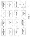
- FIG. 1 is a flow chart of a method 100 of fabricating a buffered finFET device in accordance with an embodiment of the invention. The fabrication method 100 is described below in conjunction with the structural diagrams in FIGS. 2 through 6 .
- FIG. 2 A top (plan) view showing select features and three cross-sectional planes of the buffered finFET device is given in FIG. 2 .
- a primary purpose of FIG. 2 is to show the locations of the three cross-sectional planes which are used in the cross-sectional drawings of FIGS. 3-6 and 9 .
- the features depicted in FIG. 2 are actually buried beneath other layers in the final finFET device.
- the first cross-sectional plane in FIG. 2 is labeled A-A' and cuts across the three fins under the gate electrode 508. In other words, the electrical current flowing through the fins when the transistor is on would flow through the A-A' plane.
- the second cross-sectional plane is labeled B-B' and is parallel to A-A'.
- the B-B' plane cuts across three drain (or source) features 512.
- the third cross-sectional plane is labeled C-C' and is perpendicular to A-A' and B-B'.
- the C-C' plane cuts lengthwise though a fin.
- FIGS. 3 through 6 depict cross-sectional views of a first device structure along the three cross-sectional planes (A-A', B-B', and C-C') at various points in the fabrication process in accordance with an embodiment of the invention.
- the fabricated device shown in FIG. 6 provides one p-n junction for radiation hardening (and noise isolation) between the channel and the base of the vertical fin-shaped structure.
- FIG. 9 depicts cross-sectional views of a second device structure along the three cross-sectional planes (A-A', B-B', and C-C') after the fabrication process in accordance with an embodiment of the invention.
- the fabricated device shown in FIG. 9 provides two p-n junctions for radiation hardening (and noise isolation) between the channel and the base of the vertical fin-shaped structure.
- the semiconductor wafer may be, for example, silicon substrate.
- the silicon substrate may be un-doped or lightly doped.
- a patterned mask for well implantation may be formed. This step may include depositing a mask layer and using lithography to pattern the mask layer to expose regions for well implantation.
- Well implantation may then be performed per block 104.
- the well implantation may form either an n-type or a p-type well region, depending on the embodiment.
- High-energy ion implantation may be used to more heavily dope a buried layer beneath upper layers of the substrate.
- the well implantation may implant dopant atoms at a density on the order of 10 17 cm -3 .
- a patterned mask for buffer implantation may be formed. This step may include depositing a mask layer and using lithography to pattern the mask layer to expose regions for buffer implantation. Buffer implantation may then be performed per block 106.
- the buffer implantation may form either a p-type or an n-type buffer layer, depending on the embodiment. In accordance with an embodiment of the invention, the well region and the buffer layer should have opposite doping polarities.
- the buffer implantation may be graded such that the upper portion of the buffer layer is more lightly doped and the lower portion of the buffer layer is more heavily doped. In one implementation, the buffer implantation may implant dopant atoms at a density on the order of 10 17 cm -3 .
- a patterned hard mask may be formed. This step may include depositing a multiple-layer hard mask and using lithography to pattern the hard mask for trench etching.
- the hard mask may include, for example, an oxide layer (silicon oxide, for example) below a nitride layer (silicon nitride, for example).
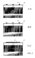
- FIG. 3 provides three cross-sectional views of a first device structure after the patterning of resist on a hard mask layer in accordance with an embodiment of the invention.
- FIG. 3 depicts an upper semiconductor layer 306, a buffer layer 304 above a well region 302.
- the buffer layer 304 and the well region 302 may be doped to be of opposite polarities, and the buffer layer 304 may be implanted so as to have a gradient in the doping profile such that the upper portion of the buffer layer is more lightly doped and the lower portion of the buffer layer is more heavily doped.
- the upper semiconductor layer 306 may be un-doped or lightly doped. As described further below, the upper semiconductor layer 306 will be used to form the channels, drains, and sources of the finFET device. Further depicted in FIG. 3 is a patterned resist layer 310 to be used for patterning the hard mask 308.
- a trench etch process may then be performed per block 108 of FIG. 1 .
- the trench etch may be performed using an anisotropic dry etch process.
- the trench etch may define the vertical fin-shaped structures which are characteristic of the finFET device.
- a corner rounding process may then be performed.
- the trenches may then be filled by an oxide fill per block 112.
- the oxide fill may be performed using a high aspect ratio oxide deposition process.
- CMP chemical-mechanical planarization
- the hard mask may act as a stop layer for the CMP.
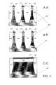
- FIG. 4 provides three cross-sectional views of the first device structure after an oxide fill and chemical-mechanical planarization in accordance with an embodiment of the invention.
- FIG. 4 depicts oxide filled trenches 402 separating the vertical fin-shaped structures 404 formed by un-etched portions beneath the hard mask 308. As depicted, the vertical fm-shaped structures 404 may widen towards its base and may extend below the buffer layer 304 into the well region 302.
- oxide recess may be performed per block 116.
- the oxide recess may be a performed, for example, by a dry recess etch process.
- the oxide recess exposes at least a portion of the upper semiconductor layer of each vertical fin-shaped structure.
- the exposed portions are fin shaped and may be referred to as the fins-shaped bodies or the fins of the device.
- a middle part of each fin will be used for the channels of the finFET device, and the side parts of each fin will be used for the sources and drains of the finFET device.
- the gate stack may then be formed over the three exposed surfaces of the channels.
- the gate stack may include a thin gate dielectric layer which is deposited over the three exposed surfaces of fin-shaped channels of the finFET device.
- the gate dielectric layer may be a gate oxide layer or a high K dielectric layer.
- the gate stack may further include a gate electrode which is formed over the thin gate oxide layer.
- the gate electrode may be made of polysilicon, for example, which may be deposited by chemical vapor deposition, or may be a metal gate electrode.
- the gate stack spacers may be formed as an oxide layer on either side of the gate electrode per block 120. The gate stack spacers serve to isolate the gate electrode from the sources and drains of the finFET device.
- source-drain extension (SDE) implantation may then be performed.
- the SDE implant may dope the drain and source extension regions such that they are n-type.
- the SDE implantation is an optional step which may be employed in some embodiments. In other embodiments, doping of the sources and drains may be accomplished by way of in situ doping during epitaxial growth of the source and drain.
- FIG. 5 provides three cross-sectional views of the first device structure after source-drain extension implantation in accordance with an embodiment of the invention.
- FIG. 5 shows that the oxide filled trenches 402 have been recessed down to a lower surface level 502 to expose fin-shaped bodies (i.e. fins) 504 of the vertical structures.
- the exposed fins 504 may include un-doped or lightly-doped channel regions 514 (shown in the A-A' and C-C' cross sections) and doped drain/source regions 512 (shown in the B-B' and C-C' cross sections).
- the A-A' cross section also shows the gate stack including the thin gate dielectric layer 506 and the gate electrode 508.
- the gate dielectric 506 is deposited over the three exposed surfaces of the channels 514.
- the gate stack spacers 510 on the sides of the gate electrode 508 are shown in the C-C' cross section.
- source/drain selective epitaxial growth is performed per block 124.
- the epitaxial growth of the source and drain may be accompanied by in situ doping of the source and drain.
- Deep source/drain implantation may then be performed per block 126.
- the deep source/drain implantation may be performed to reduce the serial resistance at the sources and drains.
- FIG. 6 shows three cross-sectional views of the first device structure after the fabrication process in accordance with an embodiment of the invention.
- the epitaxial grown portions 602 of the source/drain regions are shown. Note that the actual geometric profile of the epitaxial grown portions 602 may be expected to differ from the simplistic geometry shown in FIG. 6 .
- the drain and source regions 512 may be doped n-type
- the channel region 514 may be un-doped or lightly-doped
- the buffer layer 304 may be doped p-type
- the well region 302 may be doped n-type.
- the drain and source regions 512 may be doped p-type
- the channel region 514 may again be un-doped or lightly-doped
- the buffer layer 304 may be doped n-type
- the well region 302 may be doped p-type.
- the buffer layer 304 effectively hardens the finFET device against charge generated by ionizing radiation. It also advantageously provides noise isolation for the device in that it makes the device less susceptible to electronic noise signals which may otherwise be transmitted up the vertical fin-shaped structure. This is because the buffer layer 304 is of opposite doping polarity compared with the well region 302 such that a p-n junction is formed between the two regions. Due to the p-n junction, the well 302 collects much or most of the charge which would have been collected by the source/drain in a conventional finFET.
- FIG. 7 is a planar view showing select features of a buffered finFET device and a neighboring well tap in accordance with an embodiment of the invention.
- the features (such as the gate electrode 508) depicted in FIG. 7 are actually buried beneath other layers in the final finFET device.
- a B-B' cross-sectional plane from FIG. 2 is shown in FIG. 7 and cuts across a drain (or source) feature 512 and the neighboring well tap 702.
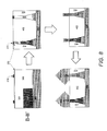
- FIG. 8 shows four cross-sectional views in the B-B' plane of FIG. 7 during the fabrication of the finFET device in accordance with an embodiment of the invention.
- the cross-sectional views shown correspond to various points in the fabrication process.
- the drain (or source) feature 512 of the buffered finFET device is being formed on the left side of each view, and the well tap 702 is being formed on the right side of each view.
- the first cross-sectional view in the upper left corner of FIG. 8 depicts the cross section after patterning of the resist layer 310 over the hard mask layer 308.
- This view shows the device at the same point in the fabrication process as FIG. 3 .
- the buffer layer 304 is formed on the left side for the buffered finFET device, but it is not formed on the right side for the well tap. Instead, the intrinsic or lightly-doped upper semiconductor layer 306 extends from the well region 302 to the hard mask layer 308 for the well tap.
- the second cross-sectional view in the upper right corner of FIG. 8 depicts the cross section after CMP of the oxide fill.
- This view shows the device at the same point in the fabrication process as FIG. 4 .
- the vertical fin-shaped structure on the right side for the well tap does not have the buffer layer 304.
- the upper semiconductor layer 306 extends from the well region 302 at the base of the vertical fin-shaped structure to the hard mask layer 308 for the well tap.
- the third cross-sectional view in the lower right corner of FIG. 8 depicts the cross section after the SDE implantation.
- This view shows the device at the same point in the fabrication process as FIG. 5 .
- a buffer layer 304 of opposite doping polarity lies beneath the drain (or source)
- the doped semiconductor layer 701 beneath the well tap is of the same doping polarity as the well tap.
- FIG. 8 depicts the cross section after selective epitaxial growth and deep source/drain implantation.
- This view shows the device at the same point in the fabrication process as FIG. 6 .
- epitaxial grown portion 602 on the drain (or source) and the epitaxial grown portion 703 for the well tap are shown.
- the well tap structure described above may be used to make an electrical connection to the well underneath the buffered finFET device.
- the well tap structure shown in FIGS. 6 and 7 has a separate fin 702 for the well connection.
- the well tap structure may use a separate planar region, instead of a separate fin, for the well connection.
- the well tap may be used to set an appropriate bias for the well of the finFET device. For example, for an n-channel finFET device, the well may be set to the supply voltage Vcc.
- FIG. 9 provides three cross-sectional views after fabrication of a second device structure in accordance with another embodiment of the invention.
- the second device structure may also be fabricated with the process steps per the method of fabrication 100 described above in relation to FIG. 1 .
- the buffer and well implants are at different depth levels (and different polarities) for the second device structure.
- the well implant 104 and buffer implant 108 steps are used to form a buffer layer 904 which separates two layers of the well region 902. This may be accomplished by a well implant 104 covering a continuous region and then a buffer implant 108 to form the buffer layer 904 in the middle of the continuous region such that the buffer layer 904 is sandwiched between the two remaining layers of the well region 902.
- the drain and source regions 512 may be doped n-type
- the channel region 514 and the well region (layers) 902 may be doped p-type
- the buffer layer 904 may be doped n-type.
- two p-n junctions are formed due to the n-type buffer layer 904 being sandwiched in the middle of two layers of the p-type well region 902.
- the drain and source regions 512 may be doped p-type
- the channel region 514 and the well region (layers) 902 may be doped n-type
- the buffer layer 904 may be doped p-type.
- two p-n junctions are formed due to the p-type buffer layer 904 being sandwiched in the middle of two layers of the n-type well region 902..
- the buffer layer 904 effectively hardens the finFET device against charge generated by ionizing radiation It also advantageously provides noise isolation for the device in that it makes the device less susceptible to electronic noise signals which may otherwise be transmitted up the vertical fin-shaped structure.
- the buffer layer 904 is of opposite doping polarity compared with the two adjacent layers of the well region 902. As such, two p-n junctions are formed between the buffer layer 904 and the two layers of the well region 902. Due to the two p-n junctions, the layer of the well region 902 near the base 406 and the buffer layer 904 collects much or most of the charge which would have been collected by the source/drain in a conventional finFET.
- additional p-n junctions besides the one or two p-n junction described above, may be created by additional implants or by implants in combination with epitaxial growth. More than two p-n junctions would provide further radiation hardening (and noise isolation), but at the cost of additional process steps.
- the buffered finFET devices disclosed herein may be used to form an SEU-resistant memory cell. It is also contemplated that the buffered finFET devices disclosed herein may be utilized to form noise-resistant analog circuits. The buffered finFET devices disclosed herein may also be used in other electronic circuits. Various types of integrated circuits, including field programmable gate arrays (FPGAs), microprocessors, application specific integrated circuits (ASICs), and so on, may utilize the buffered finFET devices disclosed herein.
- FPGAs field programmable gate arrays
- ASICs application specific integrated circuits
- FIG. 10 is a simplified partial block diagram of an FPGA 1000 that can include aspects of the present invention.
- CRAM cells and/or analog circuits in the FPGA 1000 may be formed using the buffered finFET devices described herein.
- the CRAM cells store the configuration data which is used to program the FPGA.
- the analog circuits may be employed, for example, for high-speed serial communication links or for other purposes.
- FPGA 900 is described herein for illustrative purposes only and that the present invention can be implemented in many different types of integrated circuits.
- embodiments of the present invention can be used in numerous types of integrated circuits such as field programmable gate arrays (FPGAs), programmable logic devices (PLDs), complex programmable logic devices (CPLDs), programmable logic arrays (PLAs), digital signal processors (DSPs), microprocessors, and application specific integrated circuits (ASICs).
- FPGAs field programmable gate arrays
- PLDs programmable logic devices
- CPLDs complex programmable logic devices
- PLAs programmable logic arrays
- DSPs digital signal processors
- ASICs application specific integrated circuits
- FPGA 1000 includes within its "core" a two-dimensional array of programmable logic array blocks (or LABs) 1002 that are interconnected by a network of column and row interconnect conductors of varying length and speed.
- LABs 1002 include multiple (e.g., ten) logic elements (or LEs).
- An LE is a programmable logic block that provides for efficient implementation of user defined logic functions.
- An FPGA has numerous logic elements that can be configured to implement various combinatorial and sequential functions.
- the logic elements have access to a programmable interconnect structure.
- the programmable interconnect structure can be programmed to interconnect the logic elements in almost any desired configuration.
- FPGA 1000 may also include a distributed memory structure including random access memory (RAM) blocks of varying sizes provided throughout the array.
- RAM random access memory
- the RAM blocks include, for example, blocks 1004, blocks 1006, and block 1008.
- These memory blocks can also include shift registers and FIFO buffers.
- FPGA 1000 may further include digital signal processing (DSP) blocks 1010 that can implement, for example, multipliers with add or subtract features.
- DSP digital signal processing
- IOEs Input/output elements
- FPGA 1000 may further include digital signal processing (DSP) blocks 1010 that can implement, for example, multipliers with add or subtract features.
- DSP digital signal processing
- IOEs Input/output elements
- Each IOE 1012 may be coupled to an external terminal (i.e., a pin) of FPGA 1000.
- FIGS. 6 and 9 include p-n junctions which cover the entire horizontal cross section of the vertical fin-shaped structures. It is contemplated that other embodiments may form a p-n junction which only partially cover the horizontal cross section of the vertical fin-shaped structure. An example of such an embodiment is depicted in FIG. 11 .
- the device in FIG. 11 differs from the device in FIG. 6 in that the buffer region 304 in FIG. 11 partially covers the horizontal cross section of the vertical fin-shaped structure.
- the uncovered portions 1102 of the horizontal cross section may be undoped or lightly doped semiconductor. This is shown in the C-C' cross section.
Landscapes
- Insulated Gate Type Field-Effect Transistor (AREA)
- Metal-Oxide And Bipolar Metal-Oxide Semiconductor Integrated Circuits (AREA)
- Semiconductor Memories (AREA)
- Element Separation (AREA)
Abstract
Description
- The present invention relates generally to integrated circuit devices.
- FinFET (fin field effect transistor) devices are non-planar transistor devices which have been developed relatively recently. FinFET devices are generally characterized by a vertical fin-shaped channel and are typically formed on silicon-on-insulator (SOI) or bulk silicon substrates.
- It is highly desirable to improve the robustness of finFET devices.
- The invention relates to a transistor device according to claim 1 and to a method of fabricating a device, especially a FINFET device. Claims 2 to 8 refer to specifically advantageous realizations of the transistor device according to claim 1, claims 10 to 17 to specifically advantageous realizations of the method according to claim 9.
- According to a further independent aspect the invention relates to an integrated circuit comprising at least one buffered finFET device, the buffered finFET device comprising:
- a buffered vertical fin-shaped structure which includes at least
- an upper semiconductor layer including a channel region in between drain and source regions, a buffer region beneath the upper semiconductor layer, the buffer region having a first doping polarity,
- at least part of a well region having a second doping polarity which is opposite to the first doping polarity, and
- at least one p-n junction between the buffer region and the well region which at least partially covers a horizontal cross section of the vertical fin-shaped structure; and a gate stack formed over the channel region of the upper semiconductor layer.
- According to a preferred embodiment of such an integrated circuit, it further comprises a well tap which bypasses the buffered vertical fin-shaped structure and electrically connects to the well region.
- According to a still further preferred embodiment of the the integrated circuit, the buffered finFET device is part of a static memory cell.
- According to a still further preferred embodiment of the integrated circuit, the buffered fm-FET device is part of an analog circuit.
- One further embodiment relates to a buffered transistor device. The device includes a buffered vertical fin-shaped structure formed in a semiconductor substrate. The vertical fin-shaped structure includes at least an upper semiconductor layer, a buffer region, and at least part of a well region. The buffer region has a first doping polarity, and the well region has a second doping polarity which is opposite to the first doping polarity. At least one p-n junction that at least partially covers a horizontal cross section of the vertical fin-shaped structure is formed between the buffer and well regions.
- Other embodiments, aspects and features are also disclosed.
-
-
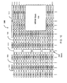
FIG. 1 is a flow chart of a method of fabricating a buffered finFET device in accordance with an embodiment of the invention. -
FIG. 2 is a planar view showing select features of a buffered finFET device in accordance with an embodiment of the invention. -
FIG. 3 shows three cross-sectional views of a first device structure after the patterning of resist on a hard mask layer in accordance with an embodiment of the invention. -
FIG. 4 shows three cross-sectional views of the first device structure after an oxide fill and chemical-mechanical planarization in accordance with an embodiment of the invention. -
FIG. 5 shows three cross-sectional views of the first device structure after source-drain extension implantation in accordance with an embodiment of the invention. -
FIG. 6 shows three cross-sectional views of the first device structure after the fabrication process in accordance with an embodiment of the invention. -
FIG. 7 is a planar view showing select features of a buffered finFET device and a neighboring well tap in accordance with an embodiment of the invention. -
FIG. 8 shows a cross-sectional view after various steps during the fabrication of the buffered finFET device and the neighboring well tap in accordance with an embodiment of the invention. -
FIG. 9 shows three cross-sectional views of the second device structure after the fabrication process in accordance with an alternate embodiment of the invention. -
FIG. 10 is a simplified partial block diagram of a field programmable gate array (FPGA) that may be configured to implement an embodiment of the present invention. -
FIG. 11 shows cross-sectional views of a device structure with a p-n junction which only partially spans a horizontal cross section of the vertical fin-shaped structure in accordance with an embodiment of the invention. - Note that the figures provided herewith are not necessarily to scale. They are provided for purposes of illustration to ease in the understanding of the presently-disclosed invention.
- Applicants have determined that the extremely small dimensions of finFET devices in memory cells make the cells susceptible to single event upsets (SEUs) and electronic noise signals. SEUs may be caused by radiation causing the generation of electron-hole pairs at a sensitive node within a cell. The operation and performance of an integrated circuit may be substantially compromised by such SEUs. For example, field programmable gate arrays (FPGAs) and other programmable logic devices (PLDs) may be particularly sensitive to SEUs occurring in configuration random access memory (CRAM) cells. Other types of integrated circuits, such as microprocessors and application specific integrated circuits (ASICS), may also be sensitive to SEUs.
- In addition, finFET devices are also susceptible to electronic noise signals which may be transmitted by way of conductive paths from other parts of an integrated circuit In particular, substrate noise may adversely impact the performance of a finFET device used in an analog circuit application.
- The present disclosure provides a buffered finFET device and method of fabricating the device. In one example application, the buffered finFET device may be utilized in static memory cells so as to substantially reduce the occurrence of SEUs in the memory cells. For instance, the buffered finFET devices may be employed in CRAM cells in FPGAs or other integrated circuits. The noise resistant feature of the buffered finFET device also makes it less susceptible to substrate noise and hence well-suited for analog circuit applications.
-
FIG. 1 is a flow chart of amethod 100 of fabricating a buffered finFET device in accordance with an embodiment of the invention. Thefabrication method 100 is described below in conjunction with the structural diagrams inFIGS. 2 through 6 . - A top (plan) view showing select features and three cross-sectional planes of the buffered finFET device is given in
FIG. 2 . Note that a primary purpose ofFIG. 2 is to show the locations of the three cross-sectional planes which are used in the cross-sectional drawings ofFIGS. 3-6 and 9 . The features depicted inFIG. 2 are actually buried beneath other layers in the final finFET device. The first cross-sectional plane inFIG. 2 is labeled A-A' and cuts across the three fins under thegate electrode 508. In other words, the electrical current flowing through the fins when the transistor is on would flow through the A-A' plane. The second cross-sectional plane is labeled B-B' and is parallel to A-A'. The B-B' plane cuts across three drain (or source) features 512. The third cross-sectional plane is labeled C-C' and is perpendicular to A-A' and B-B'. The C-C' plane cuts lengthwise though a fin. -
FIGS. 3 through 6 depict cross-sectional views of a first device structure along the three cross-sectional planes (A-A', B-B', and C-C') at various points in the fabrication process in accordance with an embodiment of the invention. The fabricated device shown inFIG. 6 provides one p-n junction for radiation hardening (and noise isolation) between the channel and the base of the vertical fin-shaped structure. -
FIG. 9 depicts cross-sectional views of a second device structure along the three cross-sectional planes (A-A', B-B', and C-C') after the fabrication process in accordance with an embodiment of the invention. The fabricated device shown inFIG. 9 provides two p-n junctions for radiation hardening (and noise isolation) between the channel and the base of the vertical fin-shaped structure. - Per
block 102, a semiconductor wafer is provided. The semiconductor wafer may be, for example, silicon substrate. The silicon substrate may be un-doped or lightly doped. - Per
block 103, a patterned mask for well implantation may be formed. This step may include depositing a mask layer and using lithography to pattern the mask layer to expose regions for well implantation. Well implantation may then be performed perblock 104. The well implantation may form either an n-type or a p-type well region, depending on the embodiment. High-energy ion implantation may be used to more heavily dope a buried layer beneath upper layers of the substrate. In one implementation, the well implantation may implant dopant atoms at a density on the order of 1017 cm-3. - Per
block 105, a patterned mask for buffer implantation may be formed. This step may include depositing a mask layer and using lithography to pattern the mask layer to expose regions for buffer implantation. Buffer implantation may then be performed perblock 106. The buffer implantation may form either a p-type or an n-type buffer layer, depending on the embodiment. In accordance with an embodiment of the invention, the well region and the buffer layer should have opposite doping polarities. The buffer implantation may be graded such that the upper portion of the buffer layer is more lightly doped and the lower portion of the buffer layer is more heavily doped. In one implementation, the buffer implantation may implant dopant atoms at a density on the order of 1017 cm-3. - Per
block 107, a patterned hard mask may be formed. This step may include depositing a multiple-layer hard mask and using lithography to pattern the hard mask for trench etching. The hard mask may include, for example, an oxide layer (silicon oxide, for example) below a nitride layer (silicon nitride, for example). -
FIG. 3 provides three cross-sectional views of a first device structure after the patterning of resist on a hard mask layer in accordance with an embodiment of the invention.FIG. 3 depicts anupper semiconductor layer 306, abuffer layer 304 above awell region 302. As mentioned above, thebuffer layer 304 and thewell region 302 may be doped to be of opposite polarities, and thebuffer layer 304 may be implanted so as to have a gradient in the doping profile such that the upper portion of the buffer layer is more lightly doped and the lower portion of the buffer layer is more heavily doped. Theupper semiconductor layer 306 may be un-doped or lightly doped. As described further below, theupper semiconductor layer 306 will be used to form the channels, drains, and sources of the finFET device. Further depicted inFIG. 3 is a patterned resistlayer 310 to be used for patterning thehard mask 308. - After the hard mask is patterned, a trench etch process may then be performed per
block 108 ofFIG. 1 . The trench etch may be performed using an anisotropic dry etch process. The trench etch may define the vertical fin-shaped structures which are characteristic of the finFET device. Perblock 110, a corner rounding process may then be performed. The trenches may then be filled by an oxide fill perblock 112. The oxide fill may be performed using a high aspect ratio oxide deposition process. Perblock 114, chemical-mechanical planarization (CMP) may be applied to planarize the surface. The hard mask may act as a stop layer for the CMP. -
FIG. 4 provides three cross-sectional views of the first device structure after an oxide fill and chemical-mechanical planarization in accordance with an embodiment of the invention.FIG. 4 depicts oxide filledtrenches 402 separating the vertical fin-shapedstructures 404 formed by un-etched portions beneath thehard mask 308. As depicted, the vertical fm-shapedstructures 404 may widen towards its base and may extend below thebuffer layer 304 into thewell region 302. - Returning to
FIG. 1 , oxide recess may be performed perblock 116. The oxide recess may be a performed, for example, by a dry recess etch process. The oxide recess exposes at least a portion of the upper semiconductor layer of each vertical fin-shaped structure. The exposed portions are fin shaped and may be referred to as the fins-shaped bodies or the fins of the device. A middle part of each fin will be used for the channels of the finFET device, and the side parts of each fin will be used for the sources and drains of the finFET device. - Per
block 118, the gate stack may then be formed over the three exposed surfaces of the channels. The gate stack may include a thin gate dielectric layer which is deposited over the three exposed surfaces of fin-shaped channels of the finFET device. The gate dielectric layer may be a gate oxide layer or a high K dielectric layer. The gate stack may further include a gate electrode which is formed over the thin gate oxide layer. The gate electrode may be made of polysilicon, for example, which may be deposited by chemical vapor deposition, or may be a metal gate electrode. Following the gate stack formation, the gate stack spacers may be formed as an oxide layer on either side of the gate electrode perblock 120. The gate stack spacers serve to isolate the gate electrode from the sources and drains of the finFET device. Perblock 122, source-drain extension (SDE) implantation may then be performed. In one implementation, where the buffer layer is p-type, the SDE implant may dope the drain and source extension regions such that they are n-type. The SDE implantation is an optional step which may be employed in some embodiments. In other embodiments, doping of the sources and drains may be accomplished by way of in situ doping during epitaxial growth of the source and drain. -
FIG. 5 provides three cross-sectional views of the first device structure after source-drain extension implantation in accordance with an embodiment of the invention.FIG. 5 shows that the oxide filledtrenches 402 have been recessed down to alower surface level 502 to expose fin-shaped bodies (i.e. fins) 504 of the vertical structures. The exposedfins 504 may include un-doped or lightly-doped channel regions 514 (shown in the A-A' and C-C' cross sections) and doped drain/source regions 512 (shown in the B-B' and C-C' cross sections). The A-A' cross section also shows the gate stack including the thingate dielectric layer 506 and thegate electrode 508. Thegate dielectric 506 is deposited over the three exposed surfaces of thechannels 514. Thegate stack spacers 510 on the sides of thegate electrode 508 are shown in the C-C' cross section. - Returning to the flowchart of
FIG. 1 , after the optional SDE implantation, source/drain selective epitaxial growth is performed perblock 124. As mentioned above, the epitaxial growth of the source and drain may be accompanied by in situ doping of the source and drain. Deep source/drain implantation may then be performed perblock 126. The deep source/drain implantation may be performed to reduce the serial resistance at the sources and drains. -
FIG. 6 shows three cross-sectional views of the first device structure after the fabrication process in accordance with an embodiment of the invention. The epitaxial grownportions 602 of the source/drain regions are shown. Note that the actual geometric profile of the epitaxial grownportions 602 may be expected to differ from the simplistic geometry shown inFIG. 6 . - In a first implementation of the fabricated device depicted in
FIG. 6 , the drain and source regions 512 (and extension 602) may be doped n-type, thechannel region 514 may be un-doped or lightly-doped, thebuffer layer 304 may be doped p-type, and thewell region 302 may be doped n-type. In this embodiment, there is a single p-n junction between the p-type buffer layer 304 and the n-type well region 302. - In a second implementation of the fabricated device depicted in
FIG. 6 , the drain and source regions 512 (and extension 602) may be doped p-type, thechannel region 514 may again be un-doped or lightly-doped, thebuffer layer 304 may be doped n-type, and thewell region 302 may be doped p-type. In this embodiment, there is a single p-n junction between the n-type buffer layer 304 and the p-type well region 302. - Advantageously, the
buffer layer 304 effectively hardens the finFET device against charge generated by ionizing radiation. It also advantageously provides noise isolation for the device in that it makes the device less susceptible to electronic noise signals which may otherwise be transmitted up the vertical fin-shaped structure. This is because thebuffer layer 304 is of opposite doping polarity compared with thewell region 302 such that a p-n junction is formed between the two regions. Due to the p-n junction, the well 302 collects much or most of the charge which would have been collected by the source/drain in a conventional finFET. -
FIG. 7 is a planar view showing select features of a buffered finFET device and a neighboring well tap in accordance with an embodiment of the invention. The features (such as the gate electrode 508) depicted inFIG. 7 are actually buried beneath other layers in the final finFET device. A B-B' cross-sectional plane fromFIG. 2 is shown inFIG. 7 and cuts across a drain (or source) feature 512 and the neighboring well tap 702. -
FIG. 8 shows four cross-sectional views in the B-B' plane ofFIG. 7 during the fabrication of the finFET device in accordance with an embodiment of the invention. The cross-sectional views shown correspond to various points in the fabrication process. The drain (or source) feature 512 of the buffered finFET device is being formed on the left side of each view, and thewell tap 702 is being formed on the right side of each view. - The first cross-sectional view in the upper left corner of
FIG. 8 depicts the cross section after patterning of the resistlayer 310 over thehard mask layer 308. This view shows the device at the same point in the fabrication process asFIG. 3 . As seen, thebuffer layer 304 is formed on the left side for the buffered finFET device, but it is not formed on the right side for the well tap. Instead, the intrinsic or lightly-dopedupper semiconductor layer 306 extends from thewell region 302 to thehard mask layer 308 for the well tap. - The second cross-sectional view in the upper right corner of
FIG. 8 depicts the cross section after CMP of the oxide fill. This view shows the device at the same point in the fabrication process asFIG. 4 . As seen, the vertical fin-shaped structure on the right side for the well tap does not have thebuffer layer 304. Instead, theupper semiconductor layer 306 extends from thewell region 302 at the base of the vertical fin-shaped structure to thehard mask layer 308 for the well tap. - The third cross-sectional view in the lower right corner of
FIG. 8 depicts the cross section after the SDE implantation. This view shows the device at the same point in the fabrication process asFIG. 5 . At this point, there is an exposed fin-shapedbody 512 on the left side for the drain (or source) and an exposed fin-shapedbody 702 on the right side for the well tap. While abuffer layer 304 of opposite doping polarity lies beneath the drain (or source), the doped semiconductor layer 701 beneath the well tap is of the same doping polarity as the well tap. - Finally, the fourth cross-sectional view in the lower left corner of
FIG. 8 depicts the cross section after selective epitaxial growth and deep source/drain implantation. This view shows the device at the same point in the fabrication process asFIG. 6 . Here, epitaxial grownportion 602 on the drain (or source), and the epitaxial grown portion 703 for the well tap are shown. - Advantageously, the well tap structure described above may be used to make an electrical connection to the well underneath the buffered finFET device. The well tap structure shown in
FIGS. 6 and7 has aseparate fin 702 for the well connection. Alternatively, the well tap structure may use a separate planar region, instead of a separate fin, for the well connection. The well tap may be used to set an appropriate bias for the well of the finFET device. For example, for an n-channel finFET device, the well may be set to the supply voltage Vcc. -
FIG. 9 provides three cross-sectional views after fabrication of a second device structure in accordance with another embodiment of the invention. The second device structure may also be fabricated with the process steps per the method offabrication 100 described above in relation toFIG. 1 . However, the buffer and well implants are at different depth levels (and different polarities) for the second device structure. - To form the second device structure per
FIG. 9 , thewell implant 104 andbuffer implant 108 steps are used to form abuffer layer 904 which separates two layers of thewell region 902. This may be accomplished by awell implant 104 covering a continuous region and then abuffer implant 108 to form thebuffer layer 904 in the middle of the continuous region such that thebuffer layer 904 is sandwiched between the two remaining layers of thewell region 902. - In a first implementation of the fabricated device depicted in
FIG. 9 , the drain and source regions 512 (and extension 602) may be doped n-type, thechannel region 514 and the well region (layers) 902 may be doped p-type, and thebuffer layer 904 may be doped n-type. In this embodiment, two p-n junctions are formed due to the n-type buffer layer 904 being sandwiched in the middle of two layers of the p-type well region 902. - In a second implementation of the fabricated device depicted in
FIG. 9 , the drain and source regions 512 (and extension 602) may be doped p-type, thechannel region 514 and the well region (layers) 902 may be doped n-type, and thebuffer layer 904 may be doped p-type. In this embodiment, two p-n junctions are formed due to the p-type buffer layer 904 being sandwiched in the middle of two layers of the n-type well region 902.. - Advantageously, the
buffer layer 904 effectively hardens the finFET device against charge generated by ionizing radiation It also advantageously provides noise isolation for the device in that it makes the device less susceptible to electronic noise signals which may otherwise be transmitted up the vertical fin-shaped structure. This is because thebuffer layer 904 is of opposite doping polarity compared with the two adjacent layers of thewell region 902. As such, two p-n junctions are formed between thebuffer layer 904 and the two layers of thewell region 902. Due to the two p-n junctions, the layer of thewell region 902 near thebase 406 and thebuffer layer 904 collects much or most of the charge which would have been collected by the source/drain in a conventional finFET. - In other embodiments, additional p-n junctions, besides the one or two p-n junction described above, may be created by additional implants or by implants in combination with epitaxial growth. More than two p-n junctions would provide further radiation hardening (and noise isolation), but at the cost of additional process steps.
- It is contemplated that the buffered finFET devices disclosed herein may be used to form an SEU-resistant memory cell. It is also contemplated that the buffered finFET devices disclosed herein may be utilized to form noise-resistant analog circuits. The buffered finFET devices disclosed herein may also be used in other electronic circuits. Various types of integrated circuits, including field programmable gate arrays (FPGAs), microprocessors, application specific integrated circuits (ASICs), and so on, may utilize the buffered finFET devices disclosed herein.
-
FIG. 10 is a simplified partial block diagram of anFPGA 1000 that can include aspects of the present invention. For example, CRAM cells and/or analog circuits in theFPGA 1000 may be formed using the buffered finFET devices described herein. During operation of the FPGA, the CRAM cells store the configuration data which is used to program the FPGA. The analog circuits may be employed, for example, for high-speed serial communication links or for other purposes. - It is to be understood that FPGA 900 is described herein for illustrative purposes only and that the present invention can be implemented in many different types of integrated circuits. In other words, it should be understood that embodiments of the present invention can be used in numerous types of integrated circuits such as field programmable gate arrays (FPGAs), programmable logic devices (PLDs), complex programmable logic devices (CPLDs), programmable logic arrays (PLAs), digital signal processors (DSPs), microprocessors, and application specific integrated circuits (ASICs).
-
FPGA 1000 includes within its "core" a two-dimensional array of programmable logic array blocks (or LABs) 1002 that are interconnected by a network of column and row interconnect conductors of varying length and speed.LABs 1002 include multiple (e.g., ten) logic elements (or LEs). - An LE is a programmable logic block that provides for efficient implementation of user defined logic functions. An FPGA has numerous logic elements that can be configured to implement various combinatorial and sequential functions. The logic elements have access to a programmable interconnect structure. The programmable interconnect structure can be programmed to interconnect the logic elements in almost any desired configuration.
-
FPGA 1000 may also include a distributed memory structure including random access memory (RAM) blocks of varying sizes provided throughout the array. The RAM blocks include, for example, blocks 1004, blocks 1006, andblock 1008. These memory blocks can also include shift registers and FIFO buffers. -
FPGA 1000 may further include digital signal processing (DSP) blocks 1010 that can implement, for example, multipliers with add or subtract features. Input/output elements (IOEs) 1012 located, in this example, around the periphery of the chip support numerous single-ended and differential input/output standards. EachIOE 1012 may be coupled to an external terminal (i.e., a pin) ofFPGA 1000. - Note that while the device structures shown in
FIGS. 6 and9 include p-n junctions which cover the entire horizontal cross section of the vertical fin-shaped structures. It is contemplated that other embodiments may form a p-n junction which only partially cover the horizontal cross section of the vertical fin-shaped structure. An example of such an embodiment is depicted inFIG. 11 . - The device in
FIG. 11 differs from the device inFIG. 6 in that thebuffer region 304 inFIG. 11 partially covers the horizontal cross section of the vertical fin-shaped structure. Theuncovered portions 1102 of the horizontal cross section may be undoped or lightly doped semiconductor. This is shown in the C-C' cross section. - In the above description, numerous specific details are given to provide a thorough understanding of embodiments of the invention. However, the above description of illustrated embodiments of the invention is not intended to be exhaustive or to limit the invention to the precise forms disclosed. One skilled in the relevant art will recognize that the invention can be practiced without one or more of the specific details, or with other methods, components, etc.
- In other instances, well-known structures or operations are not shown or described in detail to avoid obscuring aspects of the invention. While specific embodiments of, and examples for, the invention are described herein for illustrative purposes, various equivalent modifications are possible within the scope of the invention, as those skilled in the relevant art will recognize. These modifications may be made to the invention in light of the above detailed description.
Claims (17)
- A transistor device comprising:a semiconductor substrate;a buffered vertical fin-shaped structure formed in the semiconductor substrate, the vertical fin-shaped structure includingan upper semiconductor layer including a channel region in between drain and source regions,a buffer region beneath the upper semiconductor layer, the buffer region having a first doping polarity,at least part of a well region having a second doping polarity which is opposite to the first doping polarity, andat least one p-n junction between the buffer region and the well region which at least partially covers a horizontal cross section of the vertical fin-shaped structure; anda gate stack formed over the channel region of the upper semiconductor layer.
- The device of claim 1, further comprising:oxide-filled trenches adjacent to the vertical fin-shaped structure.
- The device according to one of claims 1 to 2, further comprising:an epitaxially-grown layer on the source and drain regions.
- The device according to one of claims 1 to 3, further comprising:gate stack spacers adjacent to the gate stack,wherein the gate stack spacers electrically isolate a gate electrode of the gate stack from the source and drain regions.
- The device according to one of claims 1 to 4, wherein the buffer region is directly above the well region such that one p-n junction is between the buffer region and the well region.
- The device according to one of claims 1 to 5, wherein a first layer of the well region is directly above the buffer region, and a second layer of the well region is directly below the buffer region at the base of the buffered vertical fin-shaped structure, such that two p-n junctions are present between the buffer region and the well region.
- The device according to one of claims 1 to 6, further comprising:a well tap which bypasses the buffered vertical fin-shaped structure and electrically connects to the well region.
- The device according to one of claims 1 to 7, wherein the horizontal cross section of the vertical fin-shaped structure is fully covered by the p-n junction.
- A method of fabricating a device, especially a finFET device, comprising a buffered vertical fin-shaped structure on a semiconductor substrate, the method comprising:implanting a well region at least partially within the vertical fin-shaped structure to be a first doping polarity; andimplanting a buffer region in the vertical fin-shaped structure to be a second doping polarity which is opposite to the first doping polarity,wherein at least one p-n junction is formed between the buffer region and the well region and at least partially covers a horizontal cross section of the vertical fin-shaped structure.
- The method of claim 9, further comprising:performing a trench etch to form trenches defining side surfaces of the vertical fin-shaped structure; andfilling the trenches with oxide.
- The method of claim 10, wherein the trench etch also forms trenches defining side surfaces of a vertical well-tap structure which bypasses the buffered vertical fin-shaped structure and electrically connects to the well region.
- The method of claim 10, further comprising:performing an oxide recess such that the oxide in the trenches is recessed so as to expose an upper semiconductor layer of the vertical fin-shaped structure.
- The method of claim 12, further comprising:forming a gate stack over a channel region of the upper semiconductor layer.
- The method of claim 13, further comprising:forming gate stack spacers adjacent to the gate stack; andperforming selective epitaxial growth on source and drain regions of the upper semiconductor layer.
- The method according to one of claims 9 to 14, wherein the buffer region is implanted directly above the well region, such that one p-n junction is formed between the buffer region and the well region.
- The method according to one of claims 9 to 14, wherein the buffer region is implanted within the well region, such that a first p-n junction is formed between the buffer region and a first layer of the well region, and a second p-n junction is formed between the buffer region and a second layer of the well region.
- The method according to one of claims 9 to 16, wherein implants of the well and buffer regions are such that the horizontal cross section of the vertical fin-shaped structure is fully covered by the at least one p-n junction.
Applications Claiming Priority (1)
| Application Number | Priority Date | Filing Date | Title |
|---|---|---|---|
| US13/214,102 US8643108B2 (en) | 2011-08-19 | 2011-08-19 | Buffered finFET device |
Publications (2)
| Publication Number | Publication Date |
|---|---|
| EP2560209A1 true EP2560209A1 (en) | 2013-02-20 |
| EP2560209B1 EP2560209B1 (en) | 2020-02-19 |
Family
ID=46727117
Family Applications (1)
| Application Number | Title | Priority Date | Filing Date |
|---|---|---|---|
| EP12180591.5A Active EP2560209B1 (en) | 2011-08-19 | 2012-08-16 | Buffered FinFET Device |
Country Status (4)
| Country | Link |
|---|---|
| US (1) | US8643108B2 (en) |
| EP (1) | EP2560209B1 (en) |
| JP (1) | JP6029885B2 (en) |
| CN (1) | CN102956692B (en) |
Cited By (2)
| Publication number | Priority date | Publication date | Assignee | Title |
|---|---|---|---|---|
| US9536882B2 (en) | 2014-12-18 | 2017-01-03 | Globalfoundries Inc. | Field-isolated bulk FinFET |
| EP3161871A4 (en) * | 2014-06-27 | 2018-02-21 | Intel Corporation | Non-linear fin-based devices |
Families Citing this family (26)
| Publication number | Priority date | Publication date | Assignee | Title |
|---|---|---|---|---|
| JP3251754B2 (en) | 1993-12-31 | 2002-01-28 | 株式会社イシダ | Weighing device with floor vibration compensation |
| US8723268B2 (en) * | 2012-06-13 | 2014-05-13 | Synopsys, Inc. | N-channel and P-channel end-to-end finFET cell architecture with relaxed gate pitch |
| US8969932B2 (en) * | 2012-12-12 | 2015-03-03 | Globalfoundries Inc. | Methods of forming a finfet semiconductor device with undoped fins |
| US9412871B2 (en) * | 2013-03-08 | 2016-08-09 | Taiwan Semiconductor Manufacturing Company, Ltd. | FinFET with channel backside passivation layer device and method |
| US9385198B2 (en) * | 2013-03-12 | 2016-07-05 | Taiwan Semiconductor Manufacturing Company, Ltd. | Heterostructures for semiconductor devices and methods of forming the same |
| WO2014209390A1 (en) * | 2013-06-28 | 2014-12-31 | Intel Corporation | Selective epitaxially grown iii-v materials based devices |
| US9892922B1 (en) | 2013-07-05 | 2018-02-13 | Altera Corporation | Methods for fabricating integrated circuits with triple gate oxide devices |
| US9093565B2 (en) | 2013-07-15 | 2015-07-28 | United Microelectronics Corp. | Fin diode structure |
| CN110047933B (en) * | 2013-09-25 | 2022-11-08 | 太浩研究有限公司 | Isolation well doped with solid state diffusion source for FINFET architecture |
| KR102130056B1 (en) * | 2013-11-15 | 2020-07-03 | 삼성전자주식회사 | Semiconductor device having fin field effect transistor and methods of forming the same |
| CN104900521B (en) * | 2014-03-04 | 2018-08-10 | 中芯国际集成电路制造(上海)有限公司 | Fin formula field effect transistor and forming method thereof |
| US10672768B2 (en) | 2014-03-17 | 2020-06-02 | Tufts University | Integrated circuit with multi-threshold bulk FinFETs |
| KR102158961B1 (en) | 2014-05-13 | 2020-09-24 | 삼성전자 주식회사 | Semiconductor device and method for fabricating the same |
| WO2016010515A1 (en) * | 2014-07-14 | 2016-01-21 | Intel Corporation | Solid-source diffused junction for fin-based electronics |
| KR102227128B1 (en) | 2014-09-03 | 2021-03-12 | 삼성전자주식회사 | Semiconductor device and method for fabricating the same |
| US9543382B1 (en) | 2015-03-19 | 2017-01-10 | Altera Corporation | FinFET with improved SEU performance |
| KR102310076B1 (en) * | 2015-04-23 | 2021-10-08 | 삼성전자주식회사 | Semiconductor devices having a source/drain ofasymmetrical shape |
| CN106356301A (en) * | 2015-07-17 | 2017-01-25 | 中芯国际集成电路制造(上海)有限公司 | Semiconductor apparatus and manufacturing method thereof |
| WO2017052612A1 (en) | 2015-09-25 | 2017-03-30 | Intel Corporation | Methods of doping fin structures of non-planar transistor devices |
| KR102323943B1 (en) | 2015-10-21 | 2021-11-08 | 삼성전자주식회사 | Method of manufacturing semiconductor device |
| KR102532202B1 (en) | 2016-01-22 | 2023-05-12 | 삼성전자 주식회사 | Semiconductor devices |
| US9780088B1 (en) | 2016-03-31 | 2017-10-03 | International Business Machines Corporation | Co-fabrication of vertical diodes and fin field effect transistors on the same substrate |
| EP3477686A4 (en) | 2016-06-28 | 2019-06-19 | Socionext Inc. | SEMICONDUCTOR DEVICE AND INTEGRATED SEMICONDUCTOR CIRCUIT |
| CN107680955B (en) | 2016-08-02 | 2020-01-21 | 中芯国际集成电路制造(北京)有限公司 | Electrostatic discharge protection device, semiconductor device, and manufacturing method |
| KR102465533B1 (en) | 2017-11-21 | 2022-11-11 | 삼성전자주식회사 | Semiconductor devices having a vertical channel |
| US10276692B1 (en) * | 2017-11-30 | 2019-04-30 | Taiwan Semiconductor Manufacturing Co., Ltd. | Fin diode structure and methods thereof |
Citations (8)
| Publication number | Priority date | Publication date | Assignee | Title |
|---|---|---|---|---|
| US6307233B1 (en) * | 1998-07-31 | 2001-10-23 | Texas Instruments Incorporated | Electrically isolated double gated transistor |
| US20040178451A1 (en) * | 1999-06-30 | 2004-09-16 | Kabushiki Kaisha Toshiba | Semiconductor device and method of manufacturing the same |
| US20050101069A1 (en) * | 2003-10-28 | 2005-05-12 | Leo Mathew | Confined spacers for double gate transistor semiconductor fabrication process |
| US20070247906A1 (en) * | 2006-03-28 | 2007-10-25 | Hiroshi Watanabe | Fin type memory cell |
| US20070257296A1 (en) * | 2006-05-01 | 2007-11-08 | Kiyotaka Miyano | Semiconductor device and method for manufacturing the same |
| WO2008036047A1 (en) * | 2006-09-21 | 2008-03-27 | Nanyang Technological University | Triple well transmit-receive switch transistor |
| US20080149984A1 (en) * | 2006-12-22 | 2008-06-26 | Chang Peter L D | Floating body memory cell having gates favoring different conductivity type regions |
| US20110074498A1 (en) * | 2009-09-30 | 2011-03-31 | Suvolta, Inc. | Electronic Devices and Systems, and Methods for Making and Using the Same |
Family Cites Families (12)
| Publication number | Priority date | Publication date | Assignee | Title |
|---|---|---|---|---|
| JP4270719B2 (en) * | 1999-06-30 | 2009-06-03 | 株式会社東芝 | Semiconductor device and manufacturing method thereof |
| US7358121B2 (en) | 2002-08-23 | 2008-04-15 | Intel Corporation | Tri-gate devices and methods of fabrication |
| US7045401B2 (en) | 2003-06-23 | 2006-05-16 | Sharp Laboratories Of America, Inc. | Strained silicon finFET device |
| KR100587672B1 (en) * | 2004-02-02 | 2006-06-08 | 삼성전자주식회사 | Fin transistor formation method using damascene method |
| TWI277210B (en) | 2004-10-26 | 2007-03-21 | Nanya Technology Corp | FinFET transistor process |
| JP4551811B2 (en) * | 2005-04-27 | 2010-09-29 | 株式会社東芝 | Manufacturing method of semiconductor device |
| US7517764B2 (en) | 2006-06-29 | 2009-04-14 | International Business Machines Corporation | Bulk FinFET device |
| WO2008039495A1 (en) * | 2006-09-27 | 2008-04-03 | Amberwave Systems Corporation | Tri-gate field-effect transistors formed by aspect ratio trapping |
| US7655989B2 (en) * | 2006-11-30 | 2010-02-02 | International Business Machines Corporation | Triple gate and double gate finFETs with different vertical dimension fins |
| JP4461154B2 (en) * | 2007-05-15 | 2010-05-12 | 株式会社東芝 | Semiconductor device |
| JP2010010473A (en) * | 2008-06-27 | 2010-01-14 | Toshiba Corp | Semiconductor device and method of manufacturing the same |
| US8557692B2 (en) | 2010-01-12 | 2013-10-15 | Taiwan Semiconductor Manufacturing Company, Ltd. | FinFET LDD and source drain implant technique |
-
2011
- 2011-08-19 US US13/214,102 patent/US8643108B2/en active Active
-
2012
- 2012-08-07 JP JP2012174990A patent/JP6029885B2/en not_active Expired - Fee Related
- 2012-08-16 EP EP12180591.5A patent/EP2560209B1/en active Active
- 2012-08-17 CN CN201210306226.5A patent/CN102956692B/en active Active
Patent Citations (8)
| Publication number | Priority date | Publication date | Assignee | Title |
|---|---|---|---|---|
| US6307233B1 (en) * | 1998-07-31 | 2001-10-23 | Texas Instruments Incorporated | Electrically isolated double gated transistor |
| US20040178451A1 (en) * | 1999-06-30 | 2004-09-16 | Kabushiki Kaisha Toshiba | Semiconductor device and method of manufacturing the same |
| US20050101069A1 (en) * | 2003-10-28 | 2005-05-12 | Leo Mathew | Confined spacers for double gate transistor semiconductor fabrication process |
| US20070247906A1 (en) * | 2006-03-28 | 2007-10-25 | Hiroshi Watanabe | Fin type memory cell |
| US20070257296A1 (en) * | 2006-05-01 | 2007-11-08 | Kiyotaka Miyano | Semiconductor device and method for manufacturing the same |
| WO2008036047A1 (en) * | 2006-09-21 | 2008-03-27 | Nanyang Technological University | Triple well transmit-receive switch transistor |
| US20080149984A1 (en) * | 2006-12-22 | 2008-06-26 | Chang Peter L D | Floating body memory cell having gates favoring different conductivity type regions |
| US20110074498A1 (en) * | 2009-09-30 | 2011-03-31 | Suvolta, Inc. | Electronic Devices and Systems, and Methods for Making and Using the Same |
Cited By (3)
| Publication number | Priority date | Publication date | Assignee | Title |
|---|---|---|---|---|
| EP3161871A4 (en) * | 2014-06-27 | 2018-02-21 | Intel Corporation | Non-linear fin-based devices |
| US10164115B2 (en) | 2014-06-27 | 2018-12-25 | Intel Corporation | Non-linear fin-based devices |
| US9536882B2 (en) | 2014-12-18 | 2017-01-03 | Globalfoundries Inc. | Field-isolated bulk FinFET |
Also Published As
| Publication number | Publication date |
|---|---|
| CN102956692B (en) | 2016-12-21 |
| JP2013046065A (en) | 2013-03-04 |
| CN102956692A (en) | 2013-03-06 |
| US8643108B2 (en) | 2014-02-04 |
| JP6029885B2 (en) | 2016-11-24 |
| EP2560209B1 (en) | 2020-02-19 |
| US20130043536A1 (en) | 2013-02-21 |
Similar Documents
| Publication | Publication Date | Title |
|---|---|---|
| US8643108B2 (en) | Buffered finFET device | |
| KR101370716B1 (en) | Semiconductor devices and manufacturing and design methods thereof | |
| US7211864B2 (en) | Fully-depleted castellated gate MOSFET device and method of manufacture thereof | |
| KR100699839B1 (en) | A semiconductor device having multiple channels and a method of manufacturing the same. | |
| US9780097B2 (en) | Dual-port SRAM devices and methods of manufacturing the same | |
| US9196543B2 (en) | Structure and method for finFET device | |
| KR100745518B1 (en) | Cmos well structure and method of forming the same | |
| US10084050B2 (en) | Semiconductor device with low-K gate cap and self-aligned contact | |
| US9570465B2 (en) | Dual STI integrated circuit including FDSOI transistors and method for manufacturing the same | |
| US7439139B2 (en) | Fully-depleted castellated gate MOSFET device and method of manufacture thereof | |
| CN119786495A (en) | Semiconductor device structure | |
| KR101585610B1 (en) | Leakage control in field effect transistors based on an implantation species introduced locally at the sti edge | |
| TW201909282A (en) | Semiconductor device and method of forming the same | |
| KR101687603B1 (en) | Fabrication process of a hybrid semiconductor substrate | |
| US7435628B1 (en) | Method of forming a vertical MOS transistor | |
| US9478642B2 (en) | Semiconductor junction formation | |
| US20210098452A1 (en) | Semiconductor Devices having Fin Field Effect Transistor (FinFET) Structures and Manufacturing and Design Methods Thereof | |
| US20250351571A1 (en) | Semiconductor devices and methods of manufacturing the same | |
| WO2018089559A1 (en) | Vertical thyristor cell and memory array with silicon germanium base regions | |
| CN107452789A (en) | Improvement layout for device manufacture | |
| US20090302421A1 (en) | Method and apparatus for creating a deep trench capacitor to improve device performance | |
| US8779476B2 (en) | Asymmetric wedge JFET, related method and design structure | |
| TW201631769A (en) | Prevention of subchannel leakage current | |
| CN106057682B (en) | A kind of integrated approach of the vertical nano-wire device of air sidewall structure | |
| CN119277761B (en) | A semiconductor static memory and its fabrication method |
Legal Events
| Date | Code | Title | Description |
|---|---|---|---|
| PUAI | Public reference made under article 153(3) epc to a published international application that has entered the european phase |
Free format text: ORIGINAL CODE: 0009012 |
|
| AK | Designated contracting states |
Kind code of ref document: A1 Designated state(s): AL AT BE BG CH CY CZ DE DK EE ES FI FR GB GR HR HU IE IS IT LI LT LU LV MC MK MT NL NO PL PT RO RS SE SI SK SM TR |
|
| AX | Request for extension of the european patent |
Extension state: BA ME |
|
| 17P | Request for examination filed |
Effective date: 20130722 |
|
| RBV | Designated contracting states (corrected) |
Designated state(s): AL AT BE BG CH CY CZ DE DK EE ES FI FR GB GR HR HU IE IS IT LI LT LU LV MC MK MT NL NO PL PT RO RS SE SI SK SM TR |
|
| STAA | Information on the status of an ep patent application or granted ep patent |
Free format text: STATUS: EXAMINATION IS IN PROGRESS |
|
| 17Q | First examination report despatched |
Effective date: 20180627 |
|
| RIC1 | Information provided on ipc code assigned before grant |
Ipc: H01L 21/336 20060101ALI20190730BHEP Ipc: H01L 21/761 20060101ALI20190730BHEP Ipc: H01L 29/78 20060101AFI20190730BHEP |
|
| GRAP | Despatch of communication of intention to grant a patent |
Free format text: ORIGINAL CODE: EPIDOSNIGR1 |
|
| STAA | Information on the status of an ep patent application or granted ep patent |
Free format text: STATUS: GRANT OF PATENT IS INTENDED |
|
| INTG | Intention to grant announced |
Effective date: 20190919 |
|
| RIN1 | Information on inventor provided before grant (corrected) |
Inventor name: WATT, JEFFREY T. Inventor name: LIU, LIN-SHIH Inventor name: XU, YANZHONG Inventor name: RAHIM, IRFAN |
|
| GRAJ | Information related to disapproval of communication of intention to grant by the applicant or resumption of examination proceedings by the epo deleted |
Free format text: ORIGINAL CODE: EPIDOSDIGR1 |
|
| STAA | Information on the status of an ep patent application or granted ep patent |
Free format text: STATUS: EXAMINATION IS IN PROGRESS |
|
| GRAR | Information related to intention to grant a patent recorded |
Free format text: ORIGINAL CODE: EPIDOSNIGR71 |
|
| GRAS | Grant fee paid |
Free format text: ORIGINAL CODE: EPIDOSNIGR3 |
|
| STAA | Information on the status of an ep patent application or granted ep patent |
Free format text: STATUS: GRANT OF PATENT IS INTENDED |
|
| INTC | Intention to grant announced (deleted) | ||
| GRAA | (expected) grant |
Free format text: ORIGINAL CODE: 0009210 |
|
| STAA | Information on the status of an ep patent application or granted ep patent |
Free format text: STATUS: THE PATENT HAS BEEN GRANTED |
|
| INTG | Intention to grant announced |
Effective date: 20200108 |
|
| AK | Designated contracting states |
Kind code of ref document: B1 Designated state(s): AL AT BE BG CH CY CZ DE DK EE ES FI FR GB GR HR HU IE IS IT LI LT LU LV MC MK MT NL NO PL PT RO RS SE SI SK SM TR |
|
| REG | Reference to a national code |
Ref country code: GB Ref legal event code: FG4D |
|
| REG | Reference to a national code |
Ref country code: CH Ref legal event code: EP |
|
| REG | Reference to a national code |
Ref country code: DE Ref legal event code: R096 Ref document number: 602012067846 Country of ref document: DE |
|
| REG | Reference to a national code |
Ref country code: AT Ref legal event code: REF Ref document number: 1235941 Country of ref document: AT Kind code of ref document: T Effective date: 20200315 |
|
| REG | Reference to a national code |
Ref country code: IE Ref legal event code: FG4D |
|
| REG | Reference to a national code |
Ref country code: NL Ref legal event code: FP |
|
| PG25 | Lapsed in a contracting state [announced via postgrant information from national office to epo] |
Ref country code: NO Free format text: LAPSE BECAUSE OF FAILURE TO SUBMIT A TRANSLATION OF THE DESCRIPTION OR TO PAY THE FEE WITHIN THE PRESCRIBED TIME-LIMIT Effective date: 20200519 Ref country code: RS Free format text: LAPSE BECAUSE OF FAILURE TO SUBMIT A TRANSLATION OF THE DESCRIPTION OR TO PAY THE FEE WITHIN THE PRESCRIBED TIME-LIMIT Effective date: 20200219 Ref country code: FI Free format text: LAPSE BECAUSE OF FAILURE TO SUBMIT A TRANSLATION OF THE DESCRIPTION OR TO PAY THE FEE WITHIN THE PRESCRIBED TIME-LIMIT Effective date: 20200219 |
|
| REG | Reference to a national code |
Ref country code: LT Ref legal event code: MG4D |
|
| PG25 | Lapsed in a contracting state [announced via postgrant information from national office to epo] |
Ref country code: LV Free format text: LAPSE BECAUSE OF FAILURE TO SUBMIT A TRANSLATION OF THE DESCRIPTION OR TO PAY THE FEE WITHIN THE PRESCRIBED TIME-LIMIT Effective date: 20200219 Ref country code: SE Free format text: LAPSE BECAUSE OF FAILURE TO SUBMIT A TRANSLATION OF THE DESCRIPTION OR TO PAY THE FEE WITHIN THE PRESCRIBED TIME-LIMIT Effective date: 20200219 Ref country code: IS Free format text: LAPSE BECAUSE OF FAILURE TO SUBMIT A TRANSLATION OF THE DESCRIPTION OR TO PAY THE FEE WITHIN THE PRESCRIBED TIME-LIMIT Effective date: 20200619 Ref country code: HR Free format text: LAPSE BECAUSE OF FAILURE TO SUBMIT A TRANSLATION OF THE DESCRIPTION OR TO PAY THE FEE WITHIN THE PRESCRIBED TIME-LIMIT Effective date: 20200219 Ref country code: GR Free format text: LAPSE BECAUSE OF FAILURE TO SUBMIT A TRANSLATION OF THE DESCRIPTION OR TO PAY THE FEE WITHIN THE PRESCRIBED TIME-LIMIT Effective date: 20200520 Ref country code: BG Free format text: LAPSE BECAUSE OF FAILURE TO SUBMIT A TRANSLATION OF THE DESCRIPTION OR TO PAY THE FEE WITHIN THE PRESCRIBED TIME-LIMIT Effective date: 20200519 |
|
| PG25 | Lapsed in a contracting state [announced via postgrant information from national office to epo] |
Ref country code: CZ Free format text: LAPSE BECAUSE OF FAILURE TO SUBMIT A TRANSLATION OF THE DESCRIPTION OR TO PAY THE FEE WITHIN THE PRESCRIBED TIME-LIMIT Effective date: 20200219 Ref country code: LT Free format text: LAPSE BECAUSE OF FAILURE TO SUBMIT A TRANSLATION OF THE DESCRIPTION OR TO PAY THE FEE WITHIN THE PRESCRIBED TIME-LIMIT Effective date: 20200219 Ref country code: SK Free format text: LAPSE BECAUSE OF FAILURE TO SUBMIT A TRANSLATION OF THE DESCRIPTION OR TO PAY THE FEE WITHIN THE PRESCRIBED TIME-LIMIT Effective date: 20200219 Ref country code: RO Free format text: LAPSE BECAUSE OF FAILURE TO SUBMIT A TRANSLATION OF THE DESCRIPTION OR TO PAY THE FEE WITHIN THE PRESCRIBED TIME-LIMIT Effective date: 20200219 Ref country code: PT Free format text: LAPSE BECAUSE OF FAILURE TO SUBMIT A TRANSLATION OF THE DESCRIPTION OR TO PAY THE FEE WITHIN THE PRESCRIBED TIME-LIMIT Effective date: 20200712 Ref country code: DK Free format text: LAPSE BECAUSE OF FAILURE TO SUBMIT A TRANSLATION OF THE DESCRIPTION OR TO PAY THE FEE WITHIN THE PRESCRIBED TIME-LIMIT Effective date: 20200219 Ref country code: SM Free format text: LAPSE BECAUSE OF FAILURE TO SUBMIT A TRANSLATION OF THE DESCRIPTION OR TO PAY THE FEE WITHIN THE PRESCRIBED TIME-LIMIT Effective date: 20200219 Ref country code: EE Free format text: LAPSE BECAUSE OF FAILURE TO SUBMIT A TRANSLATION OF THE DESCRIPTION OR TO PAY THE FEE WITHIN THE PRESCRIBED TIME-LIMIT Effective date: 20200219 Ref country code: ES Free format text: LAPSE BECAUSE OF FAILURE TO SUBMIT A TRANSLATION OF THE DESCRIPTION OR TO PAY THE FEE WITHIN THE PRESCRIBED TIME-LIMIT Effective date: 20200219 |
|
| REG | Reference to a national code |
Ref country code: AT Ref legal event code: MK05 Ref document number: 1235941 Country of ref document: AT Kind code of ref document: T Effective date: 20200219 |
|
| REG | Reference to a national code |
Ref country code: DE Ref legal event code: R097 Ref document number: 602012067846 Country of ref document: DE |
|
| PLBE | No opposition filed within time limit |
Free format text: ORIGINAL CODE: 0009261 |
|
| STAA | Information on the status of an ep patent application or granted ep patent |
Free format text: STATUS: NO OPPOSITION FILED WITHIN TIME LIMIT |
|
| 26N | No opposition filed |
Effective date: 20201120 |
|
| PG25 | Lapsed in a contracting state [announced via postgrant information from national office to epo] |
Ref country code: AT Free format text: LAPSE BECAUSE OF FAILURE TO SUBMIT A TRANSLATION OF THE DESCRIPTION OR TO PAY THE FEE WITHIN THE PRESCRIBED TIME-LIMIT Effective date: 20200219 Ref country code: IT Free format text: LAPSE BECAUSE OF FAILURE TO SUBMIT A TRANSLATION OF THE DESCRIPTION OR TO PAY THE FEE WITHIN THE PRESCRIBED TIME-LIMIT Effective date: 20200219 |
|
| PG25 | Lapsed in a contracting state [announced via postgrant information from national office to epo] |
Ref country code: SI Free format text: LAPSE BECAUSE OF FAILURE TO SUBMIT A TRANSLATION OF THE DESCRIPTION OR TO PAY THE FEE WITHIN THE PRESCRIBED TIME-LIMIT Effective date: 20200219 Ref country code: PL Free format text: LAPSE BECAUSE OF FAILURE TO SUBMIT A TRANSLATION OF THE DESCRIPTION OR TO PAY THE FEE WITHIN THE PRESCRIBED TIME-LIMIT Effective date: 20200219 |
|
| PG25 | Lapsed in a contracting state [announced via postgrant information from national office to epo] |
Ref country code: MC Free format text: LAPSE BECAUSE OF FAILURE TO SUBMIT A TRANSLATION OF THE DESCRIPTION OR TO PAY THE FEE WITHIN THE PRESCRIBED TIME-LIMIT Effective date: 20200219 |
|
| REG | Reference to a national code |
Ref country code: CH Ref legal event code: PL |
|
| PG25 | Lapsed in a contracting state [announced via postgrant information from national office to epo] |
Ref country code: LU Free format text: LAPSE BECAUSE OF NON-PAYMENT OF DUE FEES Effective date: 20200816 Ref country code: LI Free format text: LAPSE BECAUSE OF NON-PAYMENT OF DUE FEES Effective date: 20200831 Ref country code: CH Free format text: LAPSE BECAUSE OF NON-PAYMENT OF DUE FEES Effective date: 20200831 |
|
| REG | Reference to a national code |
Ref country code: BE Ref legal event code: MM Effective date: 20200831 |
|
| PG25 | Lapsed in a contracting state [announced via postgrant information from national office to epo] |
Ref country code: BE Free format text: LAPSE BECAUSE OF NON-PAYMENT OF DUE FEES Effective date: 20200831 Ref country code: IE Free format text: LAPSE BECAUSE OF NON-PAYMENT OF DUE FEES Effective date: 20200816 |
|
| PG25 | Lapsed in a contracting state [announced via postgrant information from national office to epo] |
Ref country code: TR Free format text: LAPSE BECAUSE OF FAILURE TO SUBMIT A TRANSLATION OF THE DESCRIPTION OR TO PAY THE FEE WITHIN THE PRESCRIBED TIME-LIMIT Effective date: 20200219 Ref country code: MT Free format text: LAPSE BECAUSE OF FAILURE TO SUBMIT A TRANSLATION OF THE DESCRIPTION OR TO PAY THE FEE WITHIN THE PRESCRIBED TIME-LIMIT Effective date: 20200219 Ref country code: CY Free format text: LAPSE BECAUSE OF FAILURE TO SUBMIT A TRANSLATION OF THE DESCRIPTION OR TO PAY THE FEE WITHIN THE PRESCRIBED TIME-LIMIT Effective date: 20200219 |
|
| PG25 | Lapsed in a contracting state [announced via postgrant information from national office to epo] |
Ref country code: MK Free format text: LAPSE BECAUSE OF FAILURE TO SUBMIT A TRANSLATION OF THE DESCRIPTION OR TO PAY THE FEE WITHIN THE PRESCRIBED TIME-LIMIT Effective date: 20200219 Ref country code: AL Free format text: LAPSE BECAUSE OF FAILURE TO SUBMIT A TRANSLATION OF THE DESCRIPTION OR TO PAY THE FEE WITHIN THE PRESCRIBED TIME-LIMIT Effective date: 20200219 |
|
| P01 | Opt-out of the competence of the unified patent court (upc) registered |
Effective date: 20230531 |
|
| REG | Reference to a national code |
Ref country code: DE Ref legal event code: R079 Ref document number: 602012067846 Country of ref document: DE Free format text: PREVIOUS MAIN CLASS: H01L0029780000 Ipc: H10D0030600000 |
|
| PGFP | Annual fee paid to national office [announced via postgrant information from national office to epo] |
Ref country code: NL Payment date: 20250724 Year of fee payment: 14 |
|
| PGFP | Annual fee paid to national office [announced via postgrant information from national office to epo] |
Ref country code: DE Payment date: 20250722 Year of fee payment: 14 |
|
| PGFP | Annual fee paid to national office [announced via postgrant information from national office to epo] |
Ref country code: GB Payment date: 20250717 Year of fee payment: 14 |
|
| PGFP | Annual fee paid to national office [announced via postgrant information from national office to epo] |
Ref country code: FR Payment date: 20250721 Year of fee payment: 14 |