EP2559739A1 - Manufacturing of diffractive pigments by fluidized bed chemical vapor deposition - Google Patents
Manufacturing of diffractive pigments by fluidized bed chemical vapor deposition Download PDFInfo
- Publication number
- EP2559739A1 EP2559739A1 EP12180384A EP12180384A EP2559739A1 EP 2559739 A1 EP2559739 A1 EP 2559739A1 EP 12180384 A EP12180384 A EP 12180384A EP 12180384 A EP12180384 A EP 12180384A EP 2559739 A1 EP2559739 A1 EP 2559739A1
- Authority
- EP
- European Patent Office
- Prior art keywords
- microstructured
- dielectric
- fluidized bed
- encapsulating
- dielectric core
- Prior art date
- Legal status (The legal status is an assumption and is not a legal conclusion. Google has not performed a legal analysis and makes no representation as to the accuracy of the status listed.)
- Granted
Links
- 239000000049 pigment Substances 0.000 title claims abstract description 43
- 238000005229 chemical vapour deposition Methods 0.000 title claims abstract description 22
- 238000004519 manufacturing process Methods 0.000 title description 10
- 238000005538 encapsulation Methods 0.000 claims abstract description 22
- 238000000151 deposition Methods 0.000 claims description 35
- 230000008021 deposition Effects 0.000 claims description 34
- 239000002243 precursor Substances 0.000 claims description 33
- 238000000034 method Methods 0.000 claims description 32
- 239000010409 thin film Substances 0.000 claims description 21
- 238000000576 coating method Methods 0.000 claims description 20
- 239000011248 coating agent Substances 0.000 claims description 17
- 239000000758 substrate Substances 0.000 claims description 17
- 239000000376 reactant Substances 0.000 claims description 16
- 229910001868 water Inorganic materials 0.000 claims description 12
- XLYOFNOQVPJJNP-UHFFFAOYSA-N water Substances O XLYOFNOQVPJJNP-UHFFFAOYSA-N 0.000 claims description 11
- 238000006243 chemical reaction Methods 0.000 claims description 9
- 239000006096 absorbing agent Substances 0.000 claims description 6
- 239000003989 dielectric material Substances 0.000 claims description 6
- 238000000678 plasma activation Methods 0.000 claims description 5
- 239000010410 layer Substances 0.000 description 84
- GWEVSGVZZGPLCZ-UHFFFAOYSA-N Titan oxide Chemical compound O=[Ti]=O GWEVSGVZZGPLCZ-UHFFFAOYSA-N 0.000 description 49
- VYPSYNLAJGMNEJ-UHFFFAOYSA-N Silicium dioxide Chemical compound O=[Si]=O VYPSYNLAJGMNEJ-UHFFFAOYSA-N 0.000 description 39
- -1 poly(ethoxyethylene) Polymers 0.000 description 36
- 239000007789 gas Substances 0.000 description 23
- 230000000694 effects Effects 0.000 description 20
- 239000004408 titanium dioxide Substances 0.000 description 20
- 239000000463 material Substances 0.000 description 18
- 239000000377 silicon dioxide Substances 0.000 description 18
- 230000003287 optical effect Effects 0.000 description 17
- 235000012239 silicon dioxide Nutrition 0.000 description 16
- 238000013461 design Methods 0.000 description 14
- 239000002245 particle Substances 0.000 description 14
- 238000005516 engineering process Methods 0.000 description 9
- BOTDANWDWHJENH-UHFFFAOYSA-N Tetraethyl orthosilicate Chemical compound CCO[Si](OCC)(OCC)OCC BOTDANWDWHJENH-UHFFFAOYSA-N 0.000 description 8
- QVGXLLKOCUKJST-UHFFFAOYSA-N atomic oxygen Chemical compound [O] QVGXLLKOCUKJST-UHFFFAOYSA-N 0.000 description 7
- 229910052751 metal Inorganic materials 0.000 description 7
- 239000002184 metal Substances 0.000 description 7
- 229910052760 oxygen Inorganic materials 0.000 description 7
- 239000001301 oxygen Substances 0.000 description 7
- 238000001228 spectrum Methods 0.000 description 7
- 239000010936 titanium Substances 0.000 description 7
- OKTJSMMVPCPJKN-UHFFFAOYSA-N Carbon Chemical compound [C] OKTJSMMVPCPJKN-UHFFFAOYSA-N 0.000 description 6
- 229910003074 TiCl4 Inorganic materials 0.000 description 6
- 230000005540 biological transmission Effects 0.000 description 6
- UQSXHKLRYXJYBZ-UHFFFAOYSA-N iron oxide Inorganic materials [Fe]=O UQSXHKLRYXJYBZ-UHFFFAOYSA-N 0.000 description 6
- 239000007788 liquid Substances 0.000 description 6
- 239000007787 solid Substances 0.000 description 6
- XJDNKRIXUMDJCW-UHFFFAOYSA-J titanium tetrachloride Chemical compound Cl[Ti](Cl)(Cl)Cl XJDNKRIXUMDJCW-UHFFFAOYSA-J 0.000 description 6
- 229910052799 carbon Inorganic materials 0.000 description 5
- 238000010586 diagram Methods 0.000 description 5
- 125000002524 organometallic group Chemical group 0.000 description 5
- 238000005240 physical vapour deposition Methods 0.000 description 5
- IJGRMHOSHXDMSA-UHFFFAOYSA-N Atomic nitrogen Chemical compound N#N IJGRMHOSHXDMSA-UHFFFAOYSA-N 0.000 description 4
- PXHVJJICTQNCMI-UHFFFAOYSA-N Nickel Chemical compound [Ni] PXHVJJICTQNCMI-UHFFFAOYSA-N 0.000 description 4
- 238000001035 drying Methods 0.000 description 4
- 239000010408 film Substances 0.000 description 4
- UQEAIHBTYFGYIE-UHFFFAOYSA-N hexamethyldisiloxane Chemical compound C[Si](C)(C)O[Si](C)(C)C UQEAIHBTYFGYIE-UHFFFAOYSA-N 0.000 description 4
- 239000000976 ink Substances 0.000 description 4
- LIVNPJMFVYWSIS-UHFFFAOYSA-N silicon monoxide Chemical compound [Si-]#[O+] LIVNPJMFVYWSIS-UHFFFAOYSA-N 0.000 description 4
- 238000012546 transfer Methods 0.000 description 4
- MCULRUJILOGHCJ-UHFFFAOYSA-N triisobutylaluminium Chemical compound CC(C)C[Al](CC(C)C)CC(C)C MCULRUJILOGHCJ-UHFFFAOYSA-N 0.000 description 4
- 238000007704 wet chemistry method Methods 0.000 description 4
- 229910003910 SiCl4 Inorganic materials 0.000 description 3
- ADCOVFLJGNWWNZ-UHFFFAOYSA-N antimony trioxide Chemical compound O=[Sb]O[Sb]=O ADCOVFLJGNWWNZ-UHFFFAOYSA-N 0.000 description 3
- 230000008901 benefit Effects 0.000 description 3
- 238000009388 chemical precipitation Methods 0.000 description 3
- 239000003086 colorant Substances 0.000 description 3
- 150000001875 compounds Chemical class 0.000 description 3
- 238000000921 elemental analysis Methods 0.000 description 3
- 238000005243 fluidization Methods 0.000 description 3
- 239000012705 liquid precursor Substances 0.000 description 3
- 150000001247 metal acetylides Chemical class 0.000 description 3
- 239000000203 mixture Substances 0.000 description 3
- 150000004767 nitrides Chemical class 0.000 description 3
- TWNQGVIAIRXVLR-UHFFFAOYSA-N oxo(oxoalumanyloxy)alumane Chemical compound O=[Al]O[Al]=O TWNQGVIAIRXVLR-UHFFFAOYSA-N 0.000 description 3
- NDLPOXTZKUMGOV-UHFFFAOYSA-N oxo(oxoferriooxy)iron hydrate Chemical compound O.O=[Fe]O[Fe]=O NDLPOXTZKUMGOV-UHFFFAOYSA-N 0.000 description 3
- BPUBBGLMJRNUCC-UHFFFAOYSA-N oxygen(2-);tantalum(5+) Chemical compound [O-2].[O-2].[O-2].[O-2].[O-2].[Ta+5].[Ta+5] BPUBBGLMJRNUCC-UHFFFAOYSA-N 0.000 description 3
- 239000003973 paint Substances 0.000 description 3
- 238000000623 plasma-assisted chemical vapour deposition Methods 0.000 description 3
- 229920000307 polymer substrate Polymers 0.000 description 3
- 230000008569 process Effects 0.000 description 3
- 238000000851 scanning transmission electron micrograph Methods 0.000 description 3
- FDNAPBUWERUEDA-UHFFFAOYSA-N silicon tetrachloride Chemical compound Cl[Si](Cl)(Cl)Cl FDNAPBUWERUEDA-UHFFFAOYSA-N 0.000 description 3
- 239000000344 soap Substances 0.000 description 3
- PBCFLUZVCVVTBY-UHFFFAOYSA-N tantalum pentoxide Inorganic materials O=[Ta](=O)O[Ta](=O)=O PBCFLUZVCVVTBY-UHFFFAOYSA-N 0.000 description 3
- 238000007725 thermal activation Methods 0.000 description 3
- ZNOKGRXACCSDPY-UHFFFAOYSA-N tungsten trioxide Chemical compound O=[W](=O)=O ZNOKGRXACCSDPY-UHFFFAOYSA-N 0.000 description 3
- VFLXBUJKRRJAKY-UHFFFAOYSA-N 13768-86-0 Chemical compound O=[Se](=O)=O VFLXBUJKRRJAKY-UHFFFAOYSA-N 0.000 description 2
- 229910017147 Fe(CO)5 Inorganic materials 0.000 description 2
- VEXZGXHMUGYJMC-UHFFFAOYSA-N Hydrochloric acid Chemical compound Cl VEXZGXHMUGYJMC-UHFFFAOYSA-N 0.000 description 2
- VQTUBCCKSQIDNK-UHFFFAOYSA-N Isobutene Chemical compound CC(C)=C VQTUBCCKSQIDNK-UHFFFAOYSA-N 0.000 description 2
- 229910052581 Si3N4 Inorganic materials 0.000 description 2
- 239000005083 Zinc sulfide Substances 0.000 description 2
- 150000004703 alkoxides Chemical class 0.000 description 2
- VSCWAEJMTAWNJL-UHFFFAOYSA-K aluminium trichloride Chemical compound Cl[Al](Cl)Cl VSCWAEJMTAWNJL-UHFFFAOYSA-K 0.000 description 2
- 238000000137 annealing Methods 0.000 description 2
- 238000013459 approach Methods 0.000 description 2
- OYLGJCQECKOTOL-UHFFFAOYSA-L barium fluoride Chemical compound [F-].[F-].[Ba+2] OYLGJCQECKOTOL-UHFFFAOYSA-L 0.000 description 2
- 229910001632 barium fluoride Inorganic materials 0.000 description 2
- 230000015572 biosynthetic process Effects 0.000 description 2
- CETPSERCERDGAM-UHFFFAOYSA-N ceric oxide Chemical compound O=[Ce]=O CETPSERCERDGAM-UHFFFAOYSA-N 0.000 description 2
- 229910000422 cerium(IV) oxide Inorganic materials 0.000 description 2
- 230000008859 change Effects 0.000 description 2
- 150000001805 chlorine compounds Chemical class 0.000 description 2
- 238000007796 conventional method Methods 0.000 description 2
- 239000007771 core particle Substances 0.000 description 2
- 238000000354 decomposition reaction Methods 0.000 description 2
- YYLGKUPAFFKGRQ-UHFFFAOYSA-N dimethyldiethoxysilane Chemical compound CCO[Si](C)(C)OCC YYLGKUPAFFKGRQ-UHFFFAOYSA-N 0.000 description 2
- 238000002149 energy-dispersive X-ray emission spectroscopy Methods 0.000 description 2
- RSIHJDGMBDPTIM-UHFFFAOYSA-N ethoxy(trimethyl)silane Chemical compound CCO[Si](C)(C)C RSIHJDGMBDPTIM-UHFFFAOYSA-N 0.000 description 2
- 229910001940 europium oxide Inorganic materials 0.000 description 2
- AEBZCFFCDTZXHP-UHFFFAOYSA-N europium(3+);oxygen(2-) Chemical compound [O-2].[O-2].[O-2].[Eu+3].[Eu+3] AEBZCFFCDTZXHP-UHFFFAOYSA-N 0.000 description 2
- 238000002474 experimental method Methods 0.000 description 2
- SZVJSHCCFOBDDC-UHFFFAOYSA-N ferrosoferric oxide Chemical compound O=[Fe]O[Fe]O[Fe]=O SZVJSHCCFOBDDC-UHFFFAOYSA-N 0.000 description 2
- WHJFNYXPKGDKBB-UHFFFAOYSA-N hafnium;methane Chemical compound C.[Hf] WHJFNYXPKGDKBB-UHFFFAOYSA-N 0.000 description 2
- 150000004820 halides Chemical class 0.000 description 2
- 229910003437 indium oxide Inorganic materials 0.000 description 2
- PJXISJQVUVHSOJ-UHFFFAOYSA-N indium(iii) oxide Chemical compound [O-2].[O-2].[O-2].[In+3].[In+3] PJXISJQVUVHSOJ-UHFFFAOYSA-N 0.000 description 2
- 239000011261 inert gas Substances 0.000 description 2
- 235000013980 iron oxide Nutrition 0.000 description 2
- 238000004518 low pressure chemical vapour deposition Methods 0.000 description 2
- 239000000395 magnesium oxide Substances 0.000 description 2
- CPLXHLVBOLITMK-UHFFFAOYSA-N magnesium oxide Inorganic materials [Mg]=O CPLXHLVBOLITMK-UHFFFAOYSA-N 0.000 description 2
- AXZKOIWUVFPNLO-UHFFFAOYSA-N magnesium;oxygen(2-) Chemical compound [O-2].[Mg+2] AXZKOIWUVFPNLO-UHFFFAOYSA-N 0.000 description 2
- 238000001000 micrograph Methods 0.000 description 2
- 238000002156 mixing Methods 0.000 description 2
- 229910052759 nickel Inorganic materials 0.000 description 2
- 229910052757 nitrogen Inorganic materials 0.000 description 2
- SIWVEOZUMHYXCS-UHFFFAOYSA-N oxo(oxoyttriooxy)yttrium Chemical compound O=[Y]O[Y]=O SIWVEOZUMHYXCS-UHFFFAOYSA-N 0.000 description 2
- RVTZCBVAJQQJTK-UHFFFAOYSA-N oxygen(2-);zirconium(4+) Chemical compound [O-2].[O-2].[Zr+4] RVTZCBVAJQQJTK-UHFFFAOYSA-N 0.000 description 2
- 238000004806 packaging method and process Methods 0.000 description 2
- 229920003023 plastic Polymers 0.000 description 2
- 239000004033 plastic Substances 0.000 description 2
- 229920000139 polyethylene terephthalate Polymers 0.000 description 2
- 239000005020 polyethylene terephthalate Substances 0.000 description 2
- 229920000915 polyvinyl chloride Polymers 0.000 description 2
- 239000004800 polyvinyl chloride Substances 0.000 description 2
- 229910003447 praseodymium oxide Inorganic materials 0.000 description 2
- OGHBATFHNDZKSO-UHFFFAOYSA-N propan-2-olate Chemical compound CC(C)[O-] OGHBATFHNDZKSO-UHFFFAOYSA-N 0.000 description 2
- 238000000926 separation method Methods 0.000 description 2
- HQVNEWCFYHHQES-UHFFFAOYSA-N silicon nitride Chemical compound N12[Si]34N5[Si]62N3[Si]51N64 HQVNEWCFYHHQES-UHFFFAOYSA-N 0.000 description 2
- 239000002356 single layer Substances 0.000 description 2
- 239000000243 solution Substances 0.000 description 2
- 238000004544 sputter deposition Methods 0.000 description 2
- XOLBLPGZBRYERU-UHFFFAOYSA-N tin dioxide Chemical compound O=[Sn]=O XOLBLPGZBRYERU-UHFFFAOYSA-N 0.000 description 2
- DENFJSAFJTVPJR-UHFFFAOYSA-N triethoxy(ethyl)silane Chemical compound CCO[Si](CC)(OCC)OCC DENFJSAFJTVPJR-UHFFFAOYSA-N 0.000 description 2
- XRADHEAKQRNYQQ-UHFFFAOYSA-K trifluoroneodymium Chemical compound F[Nd](F)F XRADHEAKQRNYQQ-UHFFFAOYSA-K 0.000 description 2
- UHUUYVZLXJHWDV-UHFFFAOYSA-N trimethyl(methylsilyloxy)silane Chemical compound C[SiH2]O[Si](C)(C)C UHUUYVZLXJHWDV-UHFFFAOYSA-N 0.000 description 2
- 229910052721 tungsten Inorganic materials 0.000 description 2
- 230000000007 visual effect Effects 0.000 description 2
- 229910052984 zinc sulfide Inorganic materials 0.000 description 2
- 229910001928 zirconium oxide Inorganic materials 0.000 description 2
- KWEKXPWNFQBJAY-UHFFFAOYSA-N (dimethyl-$l^{3}-silanyl)oxy-dimethylsilicon Chemical compound C[Si](C)O[Si](C)C KWEKXPWNFQBJAY-UHFFFAOYSA-N 0.000 description 1
- NGCRLFIYVFOUMZ-UHFFFAOYSA-N 2,3-dichloroquinoxaline-6-carbonyl chloride Chemical compound N1=C(Cl)C(Cl)=NC2=CC(C(=O)Cl)=CC=C21 NGCRLFIYVFOUMZ-UHFFFAOYSA-N 0.000 description 1
- SDTMFDGELKWGFT-UHFFFAOYSA-N 2-methylpropan-2-olate Chemical compound CC(C)(C)[O-] SDTMFDGELKWGFT-UHFFFAOYSA-N 0.000 description 1
- 244000215068 Acacia senegal Species 0.000 description 1
- KLZUFWVZNOTSEM-UHFFFAOYSA-K Aluminium flouride Chemical compound F[Al](F)F KLZUFWVZNOTSEM-UHFFFAOYSA-K 0.000 description 1
- 229920000084 Gum arabic Polymers 0.000 description 1
- 244000043261 Hevea brasiliensis Species 0.000 description 1
- 239000004354 Hydroxyethyl cellulose Substances 0.000 description 1
- 229920000663 Hydroxyethyl cellulose Polymers 0.000 description 1
- CBENFWSGALASAD-UHFFFAOYSA-N Ozone Chemical compound [O-][O+]=O CBENFWSGALASAD-UHFFFAOYSA-N 0.000 description 1
- 229920002319 Poly(methyl acrylate) Polymers 0.000 description 1
- 239000005062 Polybutadiene Substances 0.000 description 1
- 239000004698 Polyethylene Substances 0.000 description 1
- 239000004372 Polyvinyl alcohol Substances 0.000 description 1
- 229910007266 Si2O Inorganic materials 0.000 description 1
- 229910010066 TiC14 Inorganic materials 0.000 description 1
- 229910010062 TiCl3 Inorganic materials 0.000 description 1
- 229910003087 TiOx Inorganic materials 0.000 description 1
- 229910008940 W(CO)6 Inorganic materials 0.000 description 1
- XLOMVQKBTHCTTD-UHFFFAOYSA-N Zinc monoxide Chemical compound [Zn]=O XLOMVQKBTHCTTD-UHFFFAOYSA-N 0.000 description 1
- 239000000205 acacia gum Substances 0.000 description 1
- 235000010489 acacia gum Nutrition 0.000 description 1
- 239000002253 acid Substances 0.000 description 1
- 238000005054 agglomeration Methods 0.000 description 1
- 230000002776 aggregation Effects 0.000 description 1
- 150000001343 alkyl silanes Chemical class 0.000 description 1
- 229910052782 aluminium Inorganic materials 0.000 description 1
- XAGFODPZIPBFFR-UHFFFAOYSA-N aluminium Chemical compound [Al] XAGFODPZIPBFFR-UHFFFAOYSA-N 0.000 description 1
- PNEYBMLMFCGWSK-UHFFFAOYSA-N aluminium oxide Inorganic materials [O-2].[O-2].[O-2].[Al+3].[Al+3] PNEYBMLMFCGWSK-UHFFFAOYSA-N 0.000 description 1
- 238000004458 analytical method Methods 0.000 description 1
- 150000003842 bromide salts Chemical class 0.000 description 1
- 239000006227 byproduct Substances 0.000 description 1
- 238000001354 calcination Methods 0.000 description 1
- WUKWITHWXAAZEY-UHFFFAOYSA-L calcium difluoride Chemical compound [F-].[F-].[Ca+2] WUKWITHWXAAZEY-UHFFFAOYSA-L 0.000 description 1
- 125000002915 carbonyl group Chemical group [*:2]C([*:1])=O 0.000 description 1
- 239000000969 carrier Substances 0.000 description 1
- 229920002301 cellulose acetate Polymers 0.000 description 1
- 229940044927 ceric oxide Drugs 0.000 description 1
- QCCDYNYSHILRDG-UHFFFAOYSA-K cerium(3+);trifluoride Chemical compound [F-].[F-].[F-].[Ce+3] QCCDYNYSHILRDG-UHFFFAOYSA-K 0.000 description 1
- 229910052804 chromium Inorganic materials 0.000 description 1
- 239000002537 cosmetic Substances 0.000 description 1
- 229910001610 cryolite Inorganic materials 0.000 description 1
- 230000001419 dependent effect Effects 0.000 description 1
- 230000001066 destructive effect Effects 0.000 description 1
- 230000006866 deterioration Effects 0.000 description 1
- 230000003292 diminished effect Effects 0.000 description 1
- 238000010894 electron beam technology Methods 0.000 description 1
- 238000004049 embossing Methods 0.000 description 1
- 238000001704 evaporation Methods 0.000 description 1
- 230000008020 evaporation Effects 0.000 description 1
- 238000000605 extraction Methods 0.000 description 1
- 239000012530 fluid Substances 0.000 description 1
- 239000005350 fused silica glass Substances 0.000 description 1
- 229910002804 graphite Inorganic materials 0.000 description 1
- 239000010439 graphite Substances 0.000 description 1
- 229910052735 hafnium Inorganic materials 0.000 description 1
- 229910000449 hafnium oxide Inorganic materials 0.000 description 1
- WIHZLLGSGQNAGK-UHFFFAOYSA-N hafnium(4+);oxygen(2-) Chemical compound [O-2].[O-2].[Hf+4] WIHZLLGSGQNAGK-UHFFFAOYSA-N 0.000 description 1
- CJNBYAVZURUTKZ-UHFFFAOYSA-N hafnium(IV) oxide Inorganic materials O=[Hf]=O CJNBYAVZURUTKZ-UHFFFAOYSA-N 0.000 description 1
- 238000010438 heat treatment Methods 0.000 description 1
- 239000012433 hydrogen halide Substances 0.000 description 1
- 229910000039 hydrogen halide Inorganic materials 0.000 description 1
- 230000007062 hydrolysis Effects 0.000 description 1
- 238000006460 hydrolysis reaction Methods 0.000 description 1
- 150000004679 hydroxides Chemical class 0.000 description 1
- 235000019447 hydroxyethyl cellulose Nutrition 0.000 description 1
- 238000010348 incorporation Methods 0.000 description 1
- AMGQUBHHOARCQH-UHFFFAOYSA-N indium;oxotin Chemical compound [In].[Sn]=O AMGQUBHHOARCQH-UHFFFAOYSA-N 0.000 description 1
- 230000006698 induction Effects 0.000 description 1
- 238000002347 injection Methods 0.000 description 1
- 239000007924 injection Substances 0.000 description 1
- 230000003993 interaction Effects 0.000 description 1
- 239000011229 interlayer Substances 0.000 description 1
- 150000004694 iodide salts Chemical class 0.000 description 1
- 229940087654 iron carbonyl Drugs 0.000 description 1
- VBMVTYDPPZVILR-UHFFFAOYSA-N iron(2+);oxygen(2-) Chemical class [O-2].[Fe+2] VBMVTYDPPZVILR-UHFFFAOYSA-N 0.000 description 1
- MRELNEQAGSRDBK-UHFFFAOYSA-N lanthanum(3+);oxygen(2-) Chemical compound [O-2].[O-2].[O-2].[La+3].[La+3] MRELNEQAGSRDBK-UHFFFAOYSA-N 0.000 description 1
- 238000005339 levitation Methods 0.000 description 1
- 239000011344 liquid material Substances 0.000 description 1
- PQXKHYXIUOZZFA-UHFFFAOYSA-M lithium fluoride Chemical compound [Li+].[F-] PQXKHYXIUOZZFA-UHFFFAOYSA-M 0.000 description 1
- ORUIBWPALBXDOA-UHFFFAOYSA-L magnesium fluoride Chemical compound [F-].[F-].[Mg+2] ORUIBWPALBXDOA-UHFFFAOYSA-L 0.000 description 1
- 238000001755 magnetron sputter deposition Methods 0.000 description 1
- 229910001512 metal fluoride Inorganic materials 0.000 description 1
- 150000002739 metals Chemical class 0.000 description 1
- 238000003801 milling Methods 0.000 description 1
- 229910052750 molybdenum Inorganic materials 0.000 description 1
- 238000000465 moulding Methods 0.000 description 1
- 229920003052 natural elastomer Polymers 0.000 description 1
- 229920001194 natural rubber Polymers 0.000 description 1
- PLDDOISOJJCEMH-UHFFFAOYSA-N neodymium(3+);oxygen(2-) Chemical compound [O-2].[O-2].[O-2].[Nd+3].[Nd+3] PLDDOISOJJCEMH-UHFFFAOYSA-N 0.000 description 1
- 230000006911 nucleation Effects 0.000 description 1
- 238000010899 nucleation Methods 0.000 description 1
- 230000003647 oxidation Effects 0.000 description 1
- 238000007254 oxidation reaction Methods 0.000 description 1
- MMKQUGHLEMYQSG-UHFFFAOYSA-N oxygen(2-);praseodymium(3+) Chemical compound [O-2].[O-2].[O-2].[Pr+3].[Pr+3] MMKQUGHLEMYQSG-UHFFFAOYSA-N 0.000 description 1
- 239000001814 pectin Substances 0.000 description 1
- 235000010987 pectin Nutrition 0.000 description 1
- 229920001277 pectin Polymers 0.000 description 1
- 230000000737 periodic effect Effects 0.000 description 1
- 230000010363 phase shift Effects 0.000 description 1
- 238000000206 photolithography Methods 0.000 description 1
- 230000000704 physical effect Effects 0.000 description 1
- 210000002381 plasma Anatomy 0.000 description 1
- 239000002985 plastic film Substances 0.000 description 1
- 229920006255 plastic film Polymers 0.000 description 1
- 229920000141 poly(maleic anhydride) Polymers 0.000 description 1
- 229920003229 poly(methyl methacrylate) Polymers 0.000 description 1
- 229920002037 poly(vinyl butyral) polymer Polymers 0.000 description 1
- 229920002401 polyacrylamide Polymers 0.000 description 1
- 229920000058 polyacrylate Polymers 0.000 description 1
- 229920002857 polybutadiene Polymers 0.000 description 1
- 239000004417 polycarbonate Substances 0.000 description 1
- 229920000515 polycarbonate Polymers 0.000 description 1
- 229920000728 polyester Polymers 0.000 description 1
- 229920000573 polyethylene Polymers 0.000 description 1
- 229920000642 polymer Polymers 0.000 description 1
- 239000004926 polymethyl methacrylate Substances 0.000 description 1
- 229920002223 polystyrene Polymers 0.000 description 1
- 229920002635 polyurethane Polymers 0.000 description 1
- 229920002689 polyvinyl acetate Polymers 0.000 description 1
- 239000011118 polyvinyl acetate Substances 0.000 description 1
- 229920002451 polyvinyl alcohol Polymers 0.000 description 1
- 229920000036 polyvinylpyrrolidone Polymers 0.000 description 1
- 239000001267 polyvinylpyrrolidone Substances 0.000 description 1
- 235000013855 polyvinylpyrrolidone Nutrition 0.000 description 1
- 238000001556 precipitation Methods 0.000 description 1
- 238000003825 pressing Methods 0.000 description 1
- 238000012545 processing Methods 0.000 description 1
- 239000000047 product Substances 0.000 description 1
- 238000002310 reflectometry Methods 0.000 description 1
- 230000010076 replication Effects 0.000 description 1
- 229920005989 resin Polymers 0.000 description 1
- 239000011347 resin Substances 0.000 description 1
- 239000012266 salt solution Substances 0.000 description 1
- OJIKOZJGHCVMDC-UHFFFAOYSA-K samarium(iii) fluoride Chemical compound F[Sm](F)F OJIKOZJGHCVMDC-UHFFFAOYSA-K 0.000 description 1
- FKTOIHSPIPYAPE-UHFFFAOYSA-N samarium(iii) oxide Chemical compound [O-2].[O-2].[O-2].[Sm+3].[Sm+3] FKTOIHSPIPYAPE-UHFFFAOYSA-N 0.000 description 1
- 238000001878 scanning electron micrograph Methods 0.000 description 1
- 238000007873 sieving Methods 0.000 description 1
- 229910052710 silicon Inorganic materials 0.000 description 1
- 239000010703 silicon Substances 0.000 description 1
- HBMJWWWQQXIZIP-UHFFFAOYSA-N silicon carbide Chemical compound [Si+]#[C-] HBMJWWWQQXIZIP-UHFFFAOYSA-N 0.000 description 1
- 239000011734 sodium Substances 0.000 description 1
- 238000003980 solgel method Methods 0.000 description 1
- 239000012706 solid chemical precursor Substances 0.000 description 1
- 239000011343 solid material Substances 0.000 description 1
- 241000894007 species Species 0.000 description 1
- 229940035637 spectrum-4 Drugs 0.000 description 1
- 238000003892 spreading Methods 0.000 description 1
- 230000007480 spreading Effects 0.000 description 1
- 239000000126 substance Substances 0.000 description 1
- YEAUATLBSVJFOY-UHFFFAOYSA-N tetraantimony hexaoxide Chemical compound O1[Sb](O2)O[Sb]3O[Sb]1O[Sb]2O3 YEAUATLBSVJFOY-UHFFFAOYSA-N 0.000 description 1
- 229910001887 tin oxide Inorganic materials 0.000 description 1
- HLLICFJUWSZHRJ-UHFFFAOYSA-N tioxidazole Chemical compound CCCOC1=CC=C2N=C(NC(=O)OC)SC2=C1 HLLICFJUWSZHRJ-UHFFFAOYSA-N 0.000 description 1
- 229910052719 titanium Inorganic materials 0.000 description 1
- JMXKSZRRTHPKDL-UHFFFAOYSA-N titanium ethoxide Chemical compound [Ti+4].CC[O-].CC[O-].CC[O-].CC[O-] JMXKSZRRTHPKDL-UHFFFAOYSA-N 0.000 description 1
- YONPGGFAJWQGJC-UHFFFAOYSA-K titanium(iii) chloride Chemical compound Cl[Ti](Cl)Cl YONPGGFAJWQGJC-UHFFFAOYSA-K 0.000 description 1
- 239000012780 transparent material Substances 0.000 description 1
- ZDHXKXAHOVTTAH-UHFFFAOYSA-N trichlorosilane Chemical compound Cl[SiH](Cl)Cl ZDHXKXAHOVTTAH-UHFFFAOYSA-N 0.000 description 1
- 239000005052 trichlorosilane Substances 0.000 description 1
- BYMUNNMMXKDFEZ-UHFFFAOYSA-K trifluorolanthanum Chemical compound F[La](F)F BYMUNNMMXKDFEZ-UHFFFAOYSA-K 0.000 description 1
- 238000011144 upstream manufacturing Methods 0.000 description 1
- 239000002966 varnish Substances 0.000 description 1
- 229920002554 vinyl polymer Polymers 0.000 description 1
- DRDVZXDWVBGGMH-UHFFFAOYSA-N zinc;sulfide Chemical compound [S-2].[Zn+2] DRDVZXDWVBGGMH-UHFFFAOYSA-N 0.000 description 1
Images







Classifications
-
- C—CHEMISTRY; METALLURGY
- C09—DYES; PAINTS; POLISHES; NATURAL RESINS; ADHESIVES; COMPOSITIONS NOT OTHERWISE PROVIDED FOR; APPLICATIONS OF MATERIALS NOT OTHERWISE PROVIDED FOR
- C09C—TREATMENT OF INORGANIC MATERIALS, OTHER THAN FIBROUS FILLERS, TO ENHANCE THEIR PIGMENTING OR FILLING PROPERTIES ; PREPARATION OF CARBON BLACK ; PREPARATION OF INORGANIC MATERIALS WHICH ARE NO SINGLE CHEMICAL COMPOUNDS AND WHICH ARE MAINLY USED AS PIGMENTS OR FILLERS
- C09C1/00—Treatment of specific inorganic materials other than fibrous fillers; Preparation of carbon black
- C09C1/0015—Pigments exhibiting interference colours, e.g. transparent platelets of appropriate thinness or flaky substrates, e.g. mica, bearing appropriate thin transparent coatings
-
- C—CHEMISTRY; METALLURGY
- C09—DYES; PAINTS; POLISHES; NATURAL RESINS; ADHESIVES; COMPOSITIONS NOT OTHERWISE PROVIDED FOR; APPLICATIONS OF MATERIALS NOT OTHERWISE PROVIDED FOR
- C09C—TREATMENT OF INORGANIC MATERIALS, OTHER THAN FIBROUS FILLERS, TO ENHANCE THEIR PIGMENTING OR FILLING PROPERTIES ; PREPARATION OF CARBON BLACK ; PREPARATION OF INORGANIC MATERIALS WHICH ARE NO SINGLE CHEMICAL COMPOUNDS AND WHICH ARE MAINLY USED AS PIGMENTS OR FILLERS
- C09C1/00—Treatment of specific inorganic materials other than fibrous fillers; Preparation of carbon black
- C09C1/0015—Pigments exhibiting interference colours, e.g. transparent platelets of appropriate thinness or flaky substrates, e.g. mica, bearing appropriate thin transparent coatings
- C09C1/0021—Pigments exhibiting interference colours, e.g. transparent platelets of appropriate thinness or flaky substrates, e.g. mica, bearing appropriate thin transparent coatings comprising a core coated with only one layer having a high or low refractive index
-
- C—CHEMISTRY; METALLURGY
- C09—DYES; PAINTS; POLISHES; NATURAL RESINS; ADHESIVES; COMPOSITIONS NOT OTHERWISE PROVIDED FOR; APPLICATIONS OF MATERIALS NOT OTHERWISE PROVIDED FOR
- C09C—TREATMENT OF INORGANIC MATERIALS, OTHER THAN FIBROUS FILLERS, TO ENHANCE THEIR PIGMENTING OR FILLING PROPERTIES ; PREPARATION OF CARBON BLACK ; PREPARATION OF INORGANIC MATERIALS WHICH ARE NO SINGLE CHEMICAL COMPOUNDS AND WHICH ARE MAINLY USED AS PIGMENTS OR FILLERS
- C09C1/00—Treatment of specific inorganic materials other than fibrous fillers; Preparation of carbon black
- C09C1/0015—Pigments exhibiting interference colours, e.g. transparent platelets of appropriate thinness or flaky substrates, e.g. mica, bearing appropriate thin transparent coatings
- C09C1/0024—Pigments exhibiting interference colours, e.g. transparent platelets of appropriate thinness or flaky substrates, e.g. mica, bearing appropriate thin transparent coatings comprising a stack of coating layers with alternating high and low refractive indices, wherein the first coating layer on the core surface has the high refractive index
-
- C—CHEMISTRY; METALLURGY
- C09—DYES; PAINTS; POLISHES; NATURAL RESINS; ADHESIVES; COMPOSITIONS NOT OTHERWISE PROVIDED FOR; APPLICATIONS OF MATERIALS NOT OTHERWISE PROVIDED FOR
- C09C—TREATMENT OF INORGANIC MATERIALS, OTHER THAN FIBROUS FILLERS, TO ENHANCE THEIR PIGMENTING OR FILLING PROPERTIES ; PREPARATION OF CARBON BLACK ; PREPARATION OF INORGANIC MATERIALS WHICH ARE NO SINGLE CHEMICAL COMPOUNDS AND WHICH ARE MAINLY USED AS PIGMENTS OR FILLERS
- C09C1/00—Treatment of specific inorganic materials other than fibrous fillers; Preparation of carbon black
- C09C1/0015—Pigments exhibiting interference colours, e.g. transparent platelets of appropriate thinness or flaky substrates, e.g. mica, bearing appropriate thin transparent coatings
- C09C1/0051—Pigments exhibiting interference colours, e.g. transparent platelets of appropriate thinness or flaky substrates, e.g. mica, bearing appropriate thin transparent coatings comprising a stack of coating layers with alternating low and high refractive indices, wherein the first coating layer on the core surface has the low refractive index
-
- C—CHEMISTRY; METALLURGY
- C09—DYES; PAINTS; POLISHES; NATURAL RESINS; ADHESIVES; COMPOSITIONS NOT OTHERWISE PROVIDED FOR; APPLICATIONS OF MATERIALS NOT OTHERWISE PROVIDED FOR
- C09C—TREATMENT OF INORGANIC MATERIALS, OTHER THAN FIBROUS FILLERS, TO ENHANCE THEIR PIGMENTING OR FILLING PROPERTIES ; PREPARATION OF CARBON BLACK ; PREPARATION OF INORGANIC MATERIALS WHICH ARE NO SINGLE CHEMICAL COMPOUNDS AND WHICH ARE MAINLY USED AS PIGMENTS OR FILLERS
- C09C3/00—Treatment in general of inorganic materials, other than fibrous fillers, to enhance their pigmenting or filling properties
- C09C3/06—Treatment with inorganic compounds
- C09C3/063—Coating
-
- C—CHEMISTRY; METALLURGY
- C01—INORGANIC CHEMISTRY
- C01P—INDEXING SCHEME RELATING TO STRUCTURAL AND PHYSICAL ASPECTS OF SOLID INORGANIC COMPOUNDS
- C01P2002/00—Crystal-structural characteristics
- C01P2002/80—Crystal-structural characteristics defined by measured data other than those specified in group C01P2002/70
- C01P2002/85—Crystal-structural characteristics defined by measured data other than those specified in group C01P2002/70 by XPS, EDX or EDAX data
-
- C—CHEMISTRY; METALLURGY
- C01—INORGANIC CHEMISTRY
- C01P—INDEXING SCHEME RELATING TO STRUCTURAL AND PHYSICAL ASPECTS OF SOLID INORGANIC COMPOUNDS
- C01P2004/00—Particle morphology
- C01P2004/01—Particle morphology depicted by an image
- C01P2004/03—Particle morphology depicted by an image obtained by SEM
-
- C—CHEMISTRY; METALLURGY
- C01—INORGANIC CHEMISTRY
- C01P—INDEXING SCHEME RELATING TO STRUCTURAL AND PHYSICAL ASPECTS OF SOLID INORGANIC COMPOUNDS
- C01P2004/00—Particle morphology
- C01P2004/01—Particle morphology depicted by an image
- C01P2004/04—Particle morphology depicted by an image obtained by TEM, STEM, STM or AFM
-
- C—CHEMISTRY; METALLURGY
- C01—INORGANIC CHEMISTRY
- C01P—INDEXING SCHEME RELATING TO STRUCTURAL AND PHYSICAL ASPECTS OF SOLID INORGANIC COMPOUNDS
- C01P2004/00—Particle morphology
- C01P2004/80—Particles consisting of a mixture of two or more inorganic phases
- C01P2004/82—Particles consisting of a mixture of two or more inorganic phases two phases having the same anion, e.g. both oxidic phases
- C01P2004/84—Particles consisting of a mixture of two or more inorganic phases two phases having the same anion, e.g. both oxidic phases one phase coated with the other
-
- C—CHEMISTRY; METALLURGY
- C09—DYES; PAINTS; POLISHES; NATURAL RESINS; ADHESIVES; COMPOSITIONS NOT OTHERWISE PROVIDED FOR; APPLICATIONS OF MATERIALS NOT OTHERWISE PROVIDED FOR
- C09C—TREATMENT OF INORGANIC MATERIALS, OTHER THAN FIBROUS FILLERS, TO ENHANCE THEIR PIGMENTING OR FILLING PROPERTIES ; PREPARATION OF CARBON BLACK ; PREPARATION OF INORGANIC MATERIALS WHICH ARE NO SINGLE CHEMICAL COMPOUNDS AND WHICH ARE MAINLY USED AS PIGMENTS OR FILLERS
- C09C2200/00—Compositional and structural details of pigments exhibiting interference colours
- C09C2200/10—Interference pigments characterized by the core material
- C09C2200/1004—Interference pigments characterized by the core material the core comprising at least one inorganic oxide, e.g. Al2O3, TiO2 or SiO2
-
- C—CHEMISTRY; METALLURGY
- C09—DYES; PAINTS; POLISHES; NATURAL RESINS; ADHESIVES; COMPOSITIONS NOT OTHERWISE PROVIDED FOR; APPLICATIONS OF MATERIALS NOT OTHERWISE PROVIDED FOR
- C09C—TREATMENT OF INORGANIC MATERIALS, OTHER THAN FIBROUS FILLERS, TO ENHANCE THEIR PIGMENTING OR FILLING PROPERTIES ; PREPARATION OF CARBON BLACK ; PREPARATION OF INORGANIC MATERIALS WHICH ARE NO SINGLE CHEMICAL COMPOUNDS AND WHICH ARE MAINLY USED AS PIGMENTS OR FILLERS
- C09C2200/00—Compositional and structural details of pigments exhibiting interference colours
- C09C2200/10—Interference pigments characterized by the core material
- C09C2200/1004—Interference pigments characterized by the core material the core comprising at least one inorganic oxide, e.g. Al2O3, TiO2 or SiO2
- C09C2200/1008—Interference pigments characterized by the core material the core comprising at least one inorganic oxide, e.g. Al2O3, TiO2 or SiO2 comprising at least one metal layer adjacent to the core material, e.g. core-M or M-core-M
-
- C—CHEMISTRY; METALLURGY
- C09—DYES; PAINTS; POLISHES; NATURAL RESINS; ADHESIVES; COMPOSITIONS NOT OTHERWISE PROVIDED FOR; APPLICATIONS OF MATERIALS NOT OTHERWISE PROVIDED FOR
- C09C—TREATMENT OF INORGANIC MATERIALS, OTHER THAN FIBROUS FILLERS, TO ENHANCE THEIR PIGMENTING OR FILLING PROPERTIES ; PREPARATION OF CARBON BLACK ; PREPARATION OF INORGANIC MATERIALS WHICH ARE NO SINGLE CHEMICAL COMPOUNDS AND WHICH ARE MAINLY USED AS PIGMENTS OR FILLERS
- C09C2210/00—Special effects or uses of interference pigments
- C09C2210/30—A layer or the substrate forming a grating
-
- C—CHEMISTRY; METALLURGY
- C09—DYES; PAINTS; POLISHES; NATURAL RESINS; ADHESIVES; COMPOSITIONS NOT OTHERWISE PROVIDED FOR; APPLICATIONS OF MATERIALS NOT OTHERWISE PROVIDED FOR
- C09C—TREATMENT OF INORGANIC MATERIALS, OTHER THAN FIBROUS FILLERS, TO ENHANCE THEIR PIGMENTING OR FILLING PROPERTIES ; PREPARATION OF CARBON BLACK ; PREPARATION OF INORGANIC MATERIALS WHICH ARE NO SINGLE CHEMICAL COMPOUNDS AND WHICH ARE MAINLY USED AS PIGMENTS OR FILLERS
- C09C2210/00—Special effects or uses of interference pigments
- C09C2210/40—Embossed layers
-
- C—CHEMISTRY; METALLURGY
- C09—DYES; PAINTS; POLISHES; NATURAL RESINS; ADHESIVES; COMPOSITIONS NOT OTHERWISE PROVIDED FOR; APPLICATIONS OF MATERIALS NOT OTHERWISE PROVIDED FOR
- C09C—TREATMENT OF INORGANIC MATERIALS, OTHER THAN FIBROUS FILLERS, TO ENHANCE THEIR PIGMENTING OR FILLING PROPERTIES ; PREPARATION OF CARBON BLACK ; PREPARATION OF INORGANIC MATERIALS WHICH ARE NO SINGLE CHEMICAL COMPOUNDS AND WHICH ARE MAINLY USED AS PIGMENTS OR FILLERS
- C09C2220/00—Methods of preparing the interference pigments
- C09C2220/20—PVD, CVD methods or coating in a gas-phase using a fluidized bed
Definitions
- the present invention relates generally to thin-film pigment flakes, and more particularly to a method of manufacturing of microstructured pigment flakes.
- Specialty pigments have been developed for use in security applications, such as anti-counterfeiting devices printed on banknotes, packaging of high-value items, seals for containers, and even for direct application to commercial items.
- security applications such as anti-counterfeiting devices printed on banknotes, packaging of high-value items, seals for containers, and even for direct application to commercial items.
- U.S. twenty-dollar Federal Reserve Note currently uses optically variable ink.
- the number "20" printed in the lower-right corner of the face of the note changes color as the viewing angle changes. This is an overt anti-counterfeiting device.
- the color-shifting effect is not reproducible by ordinary color photocopiers, and someone receiving a note can observe whether it has the color-shifting security feature to determine the note's authenticity.
- iridescent pigments or diffractive pigments are used in paints and inks that are applied directly to an article, such as a stock certificate, passport, original product packaging, or to seals that are applied to an article.
- Security features that are more difficult to counterfeit are desirable as counterfeiters continue to become more sophisticated.
- One anti-counterfeiting approach uses microscopic symbols on multi-layer color-shifting pigment flakes.
- the symbols are formed on at least one of the layers of the multi-layer color-shifting pigment flakes by a local change of an optical property(s), such as reflectivity.
- the multi-layer color-shifting pigment flakes may have an all-dielectric design, or a metal-dielectric design.
- the symbols may be stamped or embossed or etched in the pigments by mechanical means or formed by laser means.
- microstructured flakes having a diffraction grating or a symbol are often need additional layers e.g. for providing a color-shifting effect.
- a conventional approach is to use roll-to roll coating.
- a roll of a sheet of polymer substrate material also known as a "web” is passed through a deposition zone and coated with one or more thin film layers. Multiple passes of the roll of polymer substrate back and forth through the deposition zone(s) may be made. The deposited coating is then separated from the polymer substrate and processed into flake.
- mass production of such pigments requires very long deposition substrates, and the roll-to-roll technology is inconvenient in this situation.
- Another object of the present invention is to provide an efficient method for manufacturing all-dielectric microstructured flakes.
- a method for forming a microstructured pigment flake includes providing a microstructured dielectric core to a fluidized bed and encapsulating the microstructured dielectric core by chemical vapor deposition while in the fluidized bed so as to form an encapsulation layer encapsulating the microstructured dielectric core.
- Another aspect of the present invention provides all-dielectric diffractive pigment flakes which include a diffractive core and one or more highly-conforming encapsulating layers, wherein the encapsulating layers are provided using chemical vapor deposition while the flakes are in the fluidized bed.
- Fig. 1 is a schematic diagram illustrating thin film interference
- Figs. 2 and 3 are schematic diagrams illustrating diffractive interference
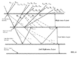
- Fig. 4 is a schematic diagram illustrating interference in a three layer High/Low/High index dielectric diffractive pigment
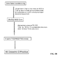
- Fig. 5A is a flow-chart of a method of manufacturing microstructured pigment flakes
- Fig. 5B is a schematic diagram illustrating manufacturing of pigment flakes
- Fig. 6 is a schematic diagram of a fluidized bed for use in FBCVD
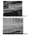
- Figs. 7A through 7D are SEM micrographs of diffractive pigment flakes
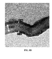
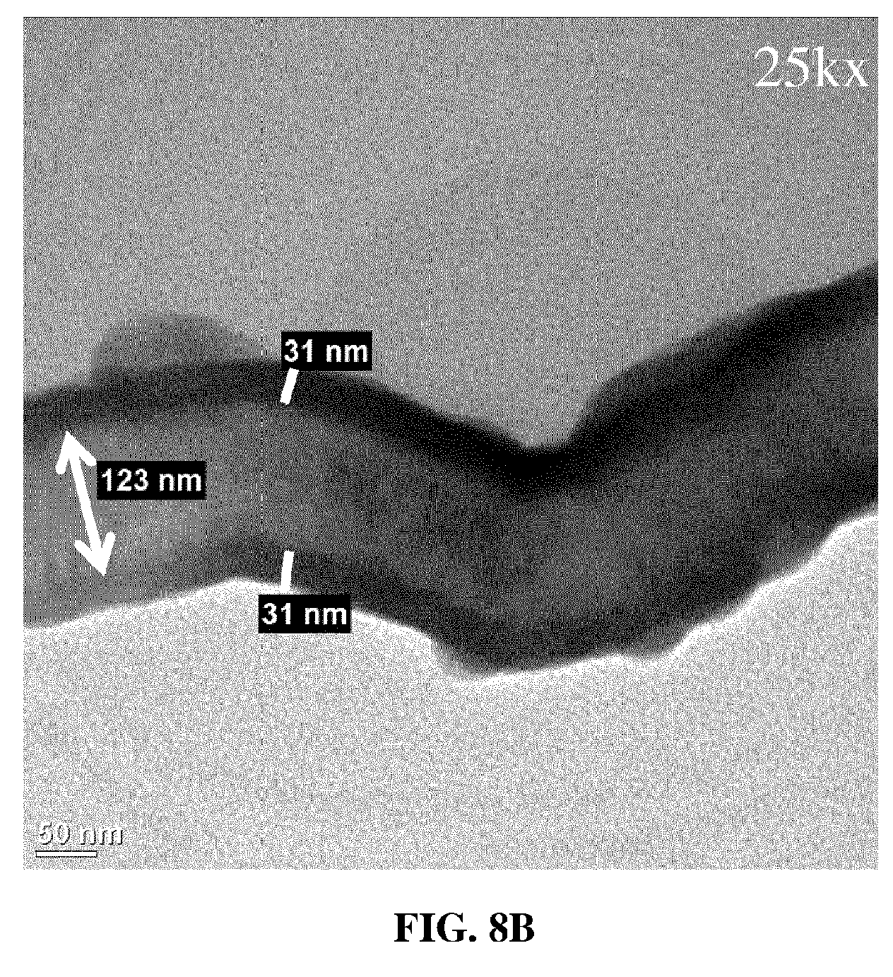
- Figs. 8A through 8C are TEM cross-sectional images of typical encapsulated flakes
- Fig. 9 is a STEM image of a flake edge
- Fig. 10 is a plot with results of elemental analysis of the spectra from the areas marked in the STEM image shown in Fig. 9 .
- the resulting micro-structured flakes exhibit a color shift with a change in viewing angle, caused by thin film interference and diffractive interference simultaneously.
- the combination of interference effects can efficiently happen only if all the interfaces between the high and low index dielectric materials layers possess the grated microstructure.
- the encapsulating layer(s) are not conforming, the diffractive effect is lost, or at least severely diminished, and the pigments exhibit only, or mostly, thin film interference. Accordingly, it is important that the technology chosen for encapsulation of diffractive core flakes be capable of reproducing the microstructure in the encapsulating layer(s). In other words, the deposited layers should be highly conforming to the original microstructure of the core flakes.
- Thin film interference occurs when a light wave encounters a boundary between semi-transparent materials with different indices of refraction, which causes the light wave to separate into a reflected and a transmitted wave.
- the reflected light beam experiences a phase shift of 180° when the second material has an index of refraction higher than the first material.
- a typical example is a soap bubble.
- the first transmitted wave travels to the internal bubble/air interface to be separated again into a reflected and a transmitted wave.
- the process repeats producing an infinite number of reflected and transmitted waves.
- the conditions for constructive and destructive interferences are different for various wavelengths of the incident white light creating the attractive colors observed in the light reflected by the soap bubble.
- a diffraction grating is an optical component made by an assembly of reflecting or transmitting elements separated by a distance comparable to the wavelength of the incident light.
- monochromatic light When monochromatic light is incident on a grating, it is diffracted in discrete directions.
- each grating grove behaves as a small, slit-shaped source of diffracted light.
- the light diffracted by each groove combines to form a diffracted wavefront.
- light incident on a grating surface at an angle that is not normal to the surface creates a zero order or specular reflection.
- the diffraction grating creates first order diffracted light beams (-1st order and 1st order) at the sides of the zero order reflection. Similarly, second and higher order diffracted lights can be created at higher angles. Diffraction can also occur on transmission as illustrated on Fig. 3 .
- an incident beam is reflected according to the laws of reflection or diffraction, and the transmitted beam can proceed in the specular direction or in a diffracted direction within the layer.
- Only the first transmitted beams which go through the High index and Low index layers to be later reflected by the High index/Low index interface are considered.
- Second internal reflections from the Low index/High index interface are shown as dash arrows and their trajectory is not considered.
- the subscripts "s" and "d” refer to specular and diffracted reflected or transmitted beams, respectively.
- R and T refer to a reflected or transmitted beam, and H and L to the High refractive index dielectric and Low refractive index dielectric layers.
- RLs represents a specular beam reflected from the High index/Low index interface layer, and THd - a diffracted beam transmitted through the Air/High index interface.
- the reflected beam labeled RHd is the only one from the Air/High index interface.
- Three other waves which traverse the layer and have undergone one diffraction are THdRLsTHs, THsRLdTHs and THsRLsTHd. These three waves interfere with each other and with the wave labeled RHd. Notice that the optical paths involved in defining the interference are not the same as for the specular beam.
- Diffractive transmitted beams (double arrowed) from the High/Low index interfaces that previously followed specular and diffractive interference at the Air/High index interference are labeled as THsTLd and THdTLd respectively.
- Fig. 4 shows optical paths of light occurring if the multilayer coating follows perfectly the grated microstructure of the core flakes. In the event the encapsulating layers fail to conform to the diffractive structure of the core, the diffractive effect does not occur and the pigment exhibits mostly thin film interference.
- the method of forming a microstructured pigment flake includes a core step 210 wherein a microstructured dielectric core is provided into a fluidized bed, and an encapsulation step 220 wherein the microstructured dielectric core is encapsulated with one or more encapsulation layers encapsulating the microstructured dielectric core; chemical vapor deposition is used while the microstructured core is in the fluidized bed.
- the core providing step 210 may include deposition of a dielectric coating on a microstructured deposition substrate 212, removing the dielectric coating 214, and breaking the dielectric coating into a plurality of cores including the microstructured dielectric core, step 216.
- Microstructured pigment flakes may include a dielectric core and one or more encapsulating layers.
- the flake core may have a microstructure formed therein, and is manufactured by deposition of one or more dielectric thin film layers on a microstructured deposition substrate, such as a plastic film, the deposition step 212, separating the thin film layer(s) from the substrate 214, and processing the separated thin film layer(s), e.g. by milling and sieving, into pre-flakes, the breaking step 216.
- the pre-flakes, or cores are encapsulated with a thin film layer during the encapsulation step 220.
- the additional encapsulating step 222 may be performed so as produce more than one encapsulating layer.
- the resulting pigment flakes are typically about 5-100 microns across, and more typically about 20-100 microns across.
- the core may include a single dielectric layer or multiple dielectric layers with a diffractive structure formed in the surface of the core.
- suitable grated microstructures are selected for the production of diffractive flakes with diffractive effects.
- the pigment flakes can include a diffractive grating microstructure with the grating frequency in the range of from about 400 grating lines per mm (ln/mm) to 4000 ln/mm in order to create a wide range of optical effects.
- the microstructure such as symbols or gratings is typically embossed or cast on the deposition substrate, and the thin film dielectric layer(s) are deposited over the embossed deposition substrate.
- the microstructure on the surface of the substrate is replicated in at least the first thin film layer that is deposited on the substrate, in either positive or negative relief. Then the coating of the thin film layer(s) is separated from the deposition substrate and processed into microstructured pre-flakes to be used as cores in the encapsulation step 220.
- the microstructured dielectric flakes may be mixed with a carrier, such as an ink vehicle or a paint vehicle, to form a composition, such as ink or paint or mixed in a clear carrier to form a varnish.
- a carrier such as an ink vehicle or a paint vehicle
- examples of carriers include polyvinyl alcohol, polyvinyl acetate polyvinylpyrrolidone, poly(ethoxyethylene), poly(methoxyethylene), poly(acrylic) acid, poly(acrylamide), poly(oxyethylene), poly(maleic anhydride), hydroxyethyl cellulose, cellulose acetate, poly(sacchrides) such as gum arabic and pectin, poly(acetals), such as polyvinylbutyral, poly(vinyl halides), such as polyvinyl chloride and polyvinylene chloride, poly(dienes) such as polybutadiene, poly(alkenes) such as polyethylene, poly(acrylates) such as polymethyl acrylate, poly(meth
Landscapes
- Chemical & Material Sciences (AREA)
- Organic Chemistry (AREA)
- Laminated Bodies (AREA)
- Pigments, Carbon Blacks, Or Wood Stains (AREA)
- Paints Or Removers (AREA)
- Diffracting Gratings Or Hologram Optical Elements (AREA)
Abstract

Description
- The present invention relates generally to thin-film pigment flakes, and more particularly to a method of manufacturing of microstructured pigment flakes.
- Specialty pigments have been developed for use in security applications, such as anti-counterfeiting devices printed on banknotes, packaging of high-value items, seals for containers, and even for direct application to commercial items. For example, the U.S. twenty-dollar Federal Reserve Note currently uses optically variable ink. The number "20" printed in the lower-right corner of the face of the note changes color as the viewing angle changes. This is an overt anti-counterfeiting device. The color-shifting effect is not reproducible by ordinary color photocopiers, and someone receiving a note can observe whether it has the color-shifting security feature to determine the note's authenticity.
- Other high-value documents and objects use similar measures. For example, iridescent pigments or diffractive pigments are used in paints and inks that are applied directly to an article, such as a stock certificate, passport, original product packaging, or to seals that are applied to an article. Security features that are more difficult to counterfeit are desirable as counterfeiters continue to become more sophisticated.
- One anti-counterfeiting approach uses microscopic symbols on multi-layer color-shifting pigment flakes. The symbols are formed on at least one of the layers of the multi-layer color-shifting pigment flakes by a local change of an optical property(s), such as reflectivity. The multi-layer color-shifting pigment flakes may have an all-dielectric design, or a metal-dielectric design. The symbols may be stamped or embossed or etched in the pigments by mechanical means or formed by laser means.
- The microstructured flakes having a diffraction grating or a symbol are often need additional layers e.g. for providing a color-shifting effect. A conventional approach is to use roll-to roll coating. A roll of a sheet of polymer substrate material (also known as a "web") is passed through a deposition zone and coated with one or more thin film layers. Multiple passes of the roll of polymer substrate back and forth through the deposition zone(s) may be made. The deposited coating is then separated from the polymer substrate and processed into flake. However, mass production of such pigments requires very long deposition substrates, and the roll-to-roll technology is inconvenient in this situation.
- Accordingly, it is desirable to provide a method of manufacturing microstructured multilayered pigment flakes that overcome the limitations of the techniques discussed above.
- All-dielectric interference structures may be formed of dielectric layers with different indices of refraction. Various combinations of these layers can be utilized to achieve the desired optically variable effect. The all-dielectric pigment flakes may be microstructured, they may include indicia for security purposes or have a diffraction grating which provides an optically variable effect.
- Another object of the present invention is to provide an efficient method for manufacturing all-dielectric microstructured flakes.
- A method is provided for forming a microstructured pigment flake. The method includes providing a microstructured dielectric core to a fluidized bed and encapsulating the microstructured dielectric core by chemical vapor deposition while in the fluidized bed so as to form an encapsulation layer encapsulating the microstructured dielectric core.
- Another aspect of the present invention provides all-dielectric diffractive pigment flakes which include a diffractive core and one or more highly-conforming encapsulating layers, wherein the encapsulating layers are provided using chemical vapor deposition while the flakes are in the fluidized bed.
- The invention will be described in greater detail with reference to the accompanying drawings which represent preferred embodiments thereof, wherein:
-
Fig. 1 is a schematic diagram illustrating thin film interference; -
Figs. 2 and 3 are schematic diagrams illustrating diffractive interference; -
Fig. 4 is a schematic diagram illustrating interference in a three layer High/Low/High index dielectric diffractive pigment; -
Fig. 5A is a flow-chart of a method of manufacturing microstructured pigment flakes; -
Fig. 5B is a schematic diagram illustrating manufacturing of pigment flakes; -
Fig. 6 is a schematic diagram of a fluidized bed for use in FBCVD; -
Figs. 7A through 7D are SEM micrographs of diffractive pigment flakes; -
Figs. 8A through 8C are TEM cross-sectional images of typical encapsulated flakes; -
Fig. 9 is a STEM image of a flake edge; and, -
Fig. 10 is a plot with results of elemental analysis of the spectra from the areas marked in the STEM image shown inFig. 9 . - A multilayer optical flake may provide a diffractive optical effect due to a diffractive microstructure on the surface of the flake, and a color-shifting effect due to light interference caused by the layered structure. The diffractive microstructure may be formed in a dielectric core which is then encapsulated with one or more encapsulation layers. It is desirable to have the coated layers totally, or at least as much as possible, conforming to the microstructure of the diffractive core in order to yield desired optical effects based on combined thin film interference of the layered coating and diffractive interference from the microstructure.
- When an all dielectric optical design is formed on a grated surface, instead of a flat surface, the resulting micro-structured flakes exhibit a color shift with a change in viewing angle, caused by thin film interference and diffractive interference simultaneously. The combination of interference effects can efficiently happen only if all the interfaces between the high and low index dielectric materials layers possess the grated microstructure. In the event the encapsulating layer(s) are not conforming, the diffractive effect is lost, or at least severely diminished, and the pigments exhibit only, or mostly, thin film interference. Accordingly, it is important that the technology chosen for encapsulation of diffractive core flakes be capable of reproducing the microstructure in the encapsulating layer(s). In other words, the deposited layers should be highly conforming to the original microstructure of the core flakes.
- Thin film interference occurs when a light wave encounters a boundary between semi-transparent materials with different indices of refraction, which causes the light wave to separate into a reflected and a transmitted wave. The reflected light beam experiences a phase shift of 180° when the second material has an index of refraction higher than the first material. A typical example is a soap bubble.
Fig. 1 illustrates a cross-section of a soap bubble (n=1.33) which is filled and surrounded by the air (n=1). The first transmitted wave travels to the internal bubble/air interface to be separated again into a reflected and a transmitted wave. The process repeats producing an infinite number of reflected and transmitted waves. The conditions for constructive and destructive interferences are different for various wavelengths of the incident white light creating the attractive colors observed in the light reflected by the soap bubble. - Diffractive interference, or diffraction, occurs when a traveling wave encounters an obstacle of dimensions similar to its wavelength. If the obstacle is periodic, some of the energy of the wave is scattered into various discrete directions (diffracted orders). Such an optical device is called a "diffraction grating."
- A diffraction grating is an optical component made by an assembly of reflecting or transmitting elements separated by a distance comparable to the wavelength of the incident light. When monochromatic light is incident on a grating, it is diffracted in discrete directions. In a grating, as shown in
Fig. 2 , each grating grove behaves as a small, slit-shaped source of diffracted light. The light diffracted by each groove combines to form a diffracted wavefront. As illustrated inFig. 2 , light incident on a grating surface at an angle that is not normal to the surface creates a zero order or specular reflection. The diffraction grating creates first order diffracted light beams (-1st order and 1st order) at the sides of the zero order reflection. Similarly, second and higher order diffracted lights can be created at higher angles. Diffraction can also occur on transmission as illustrated onFig. 3 . - The combination of the thin film and diffractive interference effects will be further discussed relative to an exemplary three-layer all-dielectric pigment of the type HLH surrounded by the air, where H stands for a high refractive index layer having a refractive index greater than 1.65 and less than 2.7 and L stands for a low refractive index layer having a refractive index less than or equal to 1.65 and greater than 1.3.
Fig. 4 schematically shows the specular and some of the diffracted beams that are reflected and/or transmitted at the Air/High index and High index/Low index interfaces boundaries of the pigment. In effect, an incident beam is reflected according to the laws of reflection or diffraction, and the transmitted beam can proceed in the specular direction or in a diffracted direction within the layer. Only the first transmitted beams which go through the High index and Low index layers to be later reflected by the High index/Low index interface are considered. Second internal reflections from the Low index/High index interface are shown as dash arrows and their trajectory is not considered. The subscripts "s" and "d" refer to specular and diffracted reflected or transmitted beams, respectively. R and T refer to a reflected or transmitted beam, and H and L to the High refractive index dielectric and Low refractive index dielectric layers. For example, with this nomenclature, RLs represents a specular beam reflected from the High index/Low index interface layer, and THd - a diffracted beam transmitted through the Air/High index interface. - Only the first specular reflected beam from the Air/High index interface (RHs) and the specular transmitted (H)/reflected (L)/transmitted(H) marked as THsRLsTHs are showed contributing to the specular reflection. Notice that this optical path is equivalent to the path for pure thin film interference.
- With respect to the diffraction, consider the waves which have undergone one diffractive interaction. The reflected beam labeled RHd is the only one from the Air/High index interface. Three other waves which traverse the layer and have undergone one diffraction are THdRLsTHs, THsRLdTHs and THsRLsTHd. These three waves interfere with each other and with the wave labeled RHd. Notice that the optical paths involved in defining the interference are not the same as for the specular beam.
- Specular transmitted beams (double arrowed) from the High/Low index interfaces that previously followed specular and diffractive interference at the Air/High index interference are labeled as THsTLs and THdTLs respectively.
- Diffractive transmitted beams (double arrowed) from the High/Low index interfaces that previously followed specular and diffractive interference at the Air/High index interference are labeled as THsTLd and THdTLd respectively.
- Even the consideration of these first few waves is complicated. For example, only the first reflected beams from the Low index/High index interface that previously followed specular and diffractive transmission from the low and high index layers are indicated. Each one of these beams will themselves follow multiples compounded intra-layer and inter-layer reflections and transmissions from both specular and diffractive interferences when entering and exiting the second high index material trough the transmission and the interface with air and/or at the Low/High index interface.
-
Fig. 4 shows optical paths of light occurring if the multilayer coating follows perfectly the grated microstructure of the core flakes. In the event the encapsulating layers fail to conform to the diffractive structure of the core, the diffractive effect does not occur and the pigment exhibits mostly thin film interference. - We have noticed that conventional encapsulation techniques such as the sol-gel method which includes decomposition of metal alkoxides in the presence of water with subsequent drying and annealing or wet chemistry based on precipitation from aqueous metallic salt solutions followed by drying and calcination fail to produce sufficiently-conforming coatings. Our experiments show that Fluidized Bed Chemical Vapor Deposition (FBCVD) technology improves the conformity of encapsulating layer(s) to microstructured dielectric pre-flakes (cores). The experimental results are discussed further with reference to
Figs. 7A-10 . - With reference to
Fig. 5A , the method of forming a microstructured pigment flake includes acore step 210 wherein a microstructured dielectric core is provided into a fluidized bed, and anencapsulation step 220 wherein the microstructured dielectric core is encapsulated with one or more encapsulation layers encapsulating the microstructured dielectric core; chemical vapor deposition is used while the microstructured core is in the fluidized bed. Thecore providing step 210 may include deposition of a dielectric coating on amicrostructured deposition substrate 212, removing thedielectric coating 214, and breaking the dielectric coating into a plurality of cores including the microstructured dielectric core,step 216. - Microstructured pigment flakes may include a dielectric core and one or more encapsulating layers. The flake core may have a microstructure formed therein, and is manufactured by deposition of one or more dielectric thin film layers on a microstructured deposition substrate, such as a plastic film, the
deposition step 212, separating the thin film layer(s) from thesubstrate 214, and processing the separated thin film layer(s), e.g. by milling and sieving, into pre-flakes, the breakingstep 216. The pre-flakes, or cores, are encapsulated with a thin film layer during theencapsulation step 220. Optionally, theadditional encapsulating step 222 may be performed so as produce more than one encapsulating layer. The resulting pigment flakes are typically about 5-100 microns across, and more typically about 20-100 microns across. - The core may include a single dielectric layer or multiple dielectric layers with a diffractive structure formed in the surface of the core. Depending on the desired optical colors and effects, suitable grated microstructures are selected for the production of diffractive flakes with diffractive effects. For example, the pigment flakes can include a diffractive grating microstructure with the grating frequency in the range of from about 400 grating lines per mm (ln/mm) to 4000 ln/mm in order to create a wide range of optical effects.
- In one embodiment, a pre-flake includes microstructured indicia, e.g. a symbol, which is typically about 0.5-20 microns in diameter. In a particular embodiment, the symbols are about 700 nanometers in diameter, and in another embodiment the symbols are about 15 microns in diameter.
- The microstructure such as symbols or gratings is typically embossed or cast on the deposition substrate, and the thin film dielectric layer(s) are deposited over the embossed deposition substrate. The microstructure on the surface of the substrate is replicated in at least the first thin film layer that is deposited on the substrate, in either positive or negative relief. Then the coating of the thin film layer(s) is separated from the deposition substrate and processed into microstructured pre-flakes to be used as cores in the
encapsulation step 220. - Preferably, the microstructured core is formed of one or more dielectric materials in order to produce semi-transparent dichroic pigments which cannot be achieved when using an opaque metal core.
- The microstructured dielectric flakes may be mixed with a carrier, such as an ink vehicle or a paint vehicle, to form a composition, such as ink or paint or mixed in a clear carrier to form a varnish. Examples of carriers include polyvinyl alcohol, polyvinyl acetate polyvinylpyrrolidone, poly(ethoxyethylene), poly(methoxyethylene), poly(acrylic) acid, poly(acrylamide), poly(oxyethylene), poly(maleic anhydride), hydroxyethyl cellulose, cellulose acetate, poly(sacchrides) such as gum arabic and pectin, poly(acetals), such as polyvinylbutyral, poly(vinyl halides), such as polyvinyl chloride and polyvinylene chloride, poly(dienes) such as polybutadiene, poly(alkenes) such as polyethylene, poly(acrylates) such as polymethyl acrylate, poly(methacrylates) such as poly methylmethacrylate, poly(carbonates) such as poly(oxycarbonyl oxyhexamethylene, poly(esters) such as polyethylene terephthalate, poly(urethanes), poly(siloxanes), poly(suphides), poly(sulphones), poly(vinylnitriles), poly(acrylonitriles), poly(styrene), poly(phenylenes) such as poly(2,5 dihydroxy-1,4-phenyleneethylene), poly(amides), natural rubbers, formaldahyde resins and other polymers.
- In one embodiment, the deposition substrate is embossed with a diffraction grating pattern. Accordingly, flake cores formed by deposition of a dielectric thin film layer onto the grated surface also have the grating pattern in one or both sides of the flakes. Alternatively, the dielectric cores may include more than one dielectric layer formed by deposition of thin film layers onto the deposition substrate prior to removing the coating and breaking it into individual pre-flakes.
- The microstructured deposition substrate which includes a microstructure such as a diffraction grating and/or symbols may be made of plastic materials such as polyvinyl chloride, polycarbonate, polyacrylate, and PET type G. The methods that can be used to form the surface relief pattern in the deposition substrate are well known by those skilled in the art. For example, a surface of the substrate may be embossed by pressing it in contact with a heated nickel embossing shim at high pressure. Other methods include photolithography and molding of the plastic substrate against a patterned surface.
- The layer(s) of microstructured flake core may be deposited using a variety of conventional techniques, such as PVD using electron beam or resistive heating evaporation, reactive DC sputtering, Radio Frequency (RF) sputtering, Magnetron sputtering, chemical vapor deposition (CVD), plasma enhanced chemical vapor deposition (PECVD), or the like.
- Suitable materials for the dielectric flake core include those having a "high" index of refraction, defined herein as greater than about 1.65, as well as those having a "low" index of refraction, which is defined herein as about 1.65 or less.
- Examples of suitable high refractive index materials for dielectric core include zinc sulfide (ZnS), zinc oxide (ZnO), zirconium oxide (ZrO2) titanium dioxide (TiO2) carbon (C), indium oxide (In2O3), indium-tin-oxide (ITO), tantalum pentoxide (Ta2O5), ceric oxide (CeO2) yttrium oxide (Y2O3), europium oxide (Eu2O3), iron oxides such as (II)diiron(III) oxide (Fe3O4) and ferric oxide (Fe2O3), hafnium nitride (HfN), hafnium carbide (HfC), hafnium oxide (HfO2 lanthanum oxide (La2O3), magnesium oxide (MgO), neodymium oxide (Nd2O3), praseodymium oxide (Pr6O11), samarium oxide (Sm2O3), antimony trioxide (Sb2O3), silicon carbide (SiC), silicon nitride (Si3N4), silicon monoxide (SiO), selenium trioxide (Se2O3), tin oxide (SnO2) tungsten trioxide (WO3) combinations thereof, and the like.
- Suitable low refractive index materials for dielectric core include silicon dioxide (SiO2), aluminum oxide (Al2O3), metal fluorides such as magnesium fluoride (MgF2), aluminum fluoride (AlF3), cerium fluoride (CeF3), lanthanum fluoride (LaF3), sodium aluminum fluorides (e.g., Na3AlF6 or Na5Al3F14), neodymium fluoride (NdF3), samarium fluoride (SmF3), barium fluoride (BaF2), calcium fluoride (CaF2), lithium fluoride (LiF), combinations thereof, or any other low index material having an index of refraction of about 1.65 or less.
-
Fig. 5B illustrates manufacturing of microstructured pigment flakes formed of high and low index dielectric materials with a symmetric design obtained by encapsulation of a core diffractive flake. Preferably, the core flake is made of a single layer of a dielectric material that can have a low or high index of refraction. In the particular example illustrated inFig. 5B , a low index dielectric core formed of SiO2 was encapsulated with a high index material TiO2 so as to produce a 3-layer (HLH) design. The TiO2 encapsulating layer was obtained by chemical vapor deposition starting with TiC14 as the precursor material in the presence of water in the form of vapor at 200C for about 1 hour following the reaction: - TiCl4 (gas) + 2 H20 (gas) → TiO2 + 4 HCL
- Suitable materials for the encapsulating layers include the same dielectric materials which may be used for the core. By way of example, a 5-layer (HLHLH) design can be obtained by encapsulation of a TiO2 core pre-flake by deposition of a layer of SiO2 followed by a layer of TiO2. In another example, a 7-layer design (HLHLHLH) - by encapsulation of a low index SiO2 diffractive core flake by consecutive layers of TiO2, SiO2 and TiO2.
- It is known in the art that the all-dielectric designs such as alternating high refractive index and low refractive index layers can provides optically variable effects depending on the thickness of the layers.
- Alternatively, the encapsulating layers may include one or more metallic absorber layers so as to form a multilayer metal-dielectric design which would provide a color shifting effect due to interference of light. By way of example, a dielectric core formed of SiO2 and encapsulated with a metal absorber such as W, Ti, Cr, Mo forms a microstructured pigment which provides a color-shifting effect due to the metal-dielectric stack. Optical designs using a high index dielectric core encapsulated with the metal absorbers produces pigments that also have very bright colors but lower color shifting effects. Multilayer designs of alternating low and high-index layers, such as HLH, LHL, HLHLH, LHLHL, can also be encapsulated with metal absorbers. If the microstructure is a diffraction grating, the pigment may provide an optically variable effect due to diffractive interference. In the event the microstructure includes indicia, the pigments may be used for security purposes because the indicia provides a covert security feature, and the color shift - an overt security feature.
- In diffractive flakes, it is desirable to have the best possible conformity of the encapsulating layer(s) to the microstructure of the core in order to yield desired visual optical effects based on diffraction, therefore we use Fluidized Bed Chemical Vapor Deposition (FBCVD) technology. The chemical vapor deposition (CVD) allows deposition of single- or multilayer coatings onto core particle surfaces; the deposited material is formed from a gaseous, liquid or solid chemical precursor. The CVD technique results in conforming encapsulating films that replicate the surface microstructure of the core flakes. The efficiency of this process depends on the contact between the surface of the particles and the film precursors. A technical solution allowing for a good contact between particles and gas precursors is to use the fluidized bed technology.
- The FBCVD method is based on a chemical reaction between a precursor and a reactant. In most cases, the precursor is oxidized with the help of the reactant so as to obtain an oxide coating on the particles. Reactants providing nitrogen and carbon can form the respective nitrides and carbides coatings. Mixtures of reactants can be used for the deposition of compounds as carbonitrides, oxycarbides, oxinitrides and even oxicarbonitrides. Both, the precursor and the reactant may be in the form of gas, liquid or solid material. Preferably, the reactant is provided in a direction opposite to the flow of the precursor. Preferably, the method includes using an inert fluidizing gas for mixing the particles. Advantageously, the chemical vapor deposition may be performed at atmospheric pressure. However, low pressure or plasma activation can be used depending on the materials of the core flakes and the films to be deposited.
- A variety of geometries can be used for the fluidized bed reactor; the fluidized bed should satisfy the constrains due to particle fluidization and chemical vapor deposition. The fluidized beds can operate under thermal or plasma activation of the reactive gas precursors accommodating for the type of particles to be treated.
- The optical effects of special effect pigments having a combination of thin film and diffractive interference are extremely dependent on the smoothly replication of the diffractive microstructure of the core diffractive pigment pre-flakes making the FBCVD technology a perfect solution for the manufacturing of special effects pigment with optical diffractive properties.
- With reference to
Fig. 6 , a fluidized bed reactor may be acylindrical vessel 100 having a porous or perforatedbottom plate 170 that is used to hold theparticles 180 and to uniformly distribute the flow of gas over the cross area of the vessel so as to obtain uniform levitation of the particles in the bed. In operation, the gas supplied though the fluidized bed moves and partially supports the particles, so that the bulk of particles expands and behaves as a fluid spreading everywhere in the vessel. Within the fluidized bed, the flow is turbulent allowing for good mass and heat transfer in between particles which is very important for uniform encapsulation by chemical vapor deposition of pigment flakes. - Compared with other deposition technologies like physical vapor deposition (PVD), the FBCVD method provides a variety of advantages. The PVD deposits the coating material mostly on the surface of the particles facing the flow of the vapor, whereas the FBCVD provides uniform coverage of the particles. Compared with PVD, the FBCVD provides not only higher growth rates due to its three dimensional growth characteristics, but also superior uniformity and conformity of the encapsulating layer(s) on microstructured core particles. This is extremely important in the case of encapsulation of diffractive pigment flakes where the surface of the flakes has symmetric alignment of groves with separation that can vary from few microns for low frequency gratings to as low as 250 nm for high frequency gratings, i.e. gratings with frequencies in the range of from 400 to 4000 grooves/mm.
- The reactors used in our experiments were made of fused quartz. An example of a fluidized bed reactor is schematically shown in
Fig. 6 . The reactor has a removable top surface (not shown) which has access ports for instrumentation, introduction of gases and liquids, and extra vibration.Arrow 110 illustrates a channel for introduction of reactant gases such as N2, NH3, H2O, CO2, H2 and/or for injection of liquid precursors from the above. Optionally, Ar, He, or other inert gases are introduced to dilute or transfer the reactant. The precursor and/or reactant may be in the liquid or solid form. Liquids or solids can be heated in containers (called bubblers for liquid precursors); inert gases are introduced into the containers to transfer the vapor of the precursors. Usually solids have a low vapor pressure and have to be heated at higher temperatures using furnaces. Fluidization conditions can be changed based on visual observation of the bed by adjusting the flow rates using flow controllers. The top surface may also have vibration means 160, such as a mechanical vibrator, and exhaust means, such as exhaust filters or scrubbers; anarrow 120 shows an exhaust flow from the exhaust means. Theinstrumentation 130 may include thermocouples, an extraction system for extracting particles to control their optical properties, and other sensor devices. - Depending of the physical properties of the coating precursors (density, vapor pressure, etc.) the
precursor 150 can be introduced upstream with the fluidizing gas (Ar, N2, He, etc.) 140 at the bottom of the reactor through asintered alumina grid 170. Individual control of the fluidizing and precursor gases before entering into the reactor allows controlling the fluidization conditions of the bed. The precursor may be coming from a bubbler, e.g. SiCl4, TiCl4, SiHCl3 precursor, or from a different source of the precursor vapor, e.g. W(CO)6, Ni (CO)6 low vapor pressure solid precursors for W and Ni metals or compounds respectively can be heated at high temperatures using closed furnaces. The fluidizing gas may be provided from a flow controller for the fluidizing gas. In case the precursor has a low vapor pressure, e.g. some organo-metallics including tetraethoxysilane (TEOS) and triisobutylaluminium (TIBA), it may be also introduced directly through the top of the reactor using a metering liquid injector; the reactant and fluidizing gases in that case are provided through the bottom of the reactor. - The FBCVD reactor can operate under thermal or plasma activation. For a thermal activation, the bed may be heated externally by a cylindrical
electric resistance furnace 150, or heated internally with a graphite susceptor and an external radio frequency (Rf) induction coil. An external Rf coil could also be used for plasma activation of the bed in case of plasma-assisted chemical vapor deposition having the advantage of non -equilibrium plasmas that can activated gaseous species at lower temperatures. In some cases, the FB reactor can have attached vacuum pumps for low pressure chemical vapor deposition (LPCVD); a vacuum pump may serve as or be part of exhaust means; filters may be used to avoid damaging the vacuum pumps. - Possible precursors include halides (chlorides, iodides and bromides). Hydrogen halide gases are by-products of the hydrolysis process.
- The FBCVD may be based on the following chemical reactions:
- TiCl4 + H20 → TiO2 + HCl
- - for Titania deposition, and
- SiCl4 + H2O → SiO2 + HCl
- - for Silica deposition.
- Oxygen or ozone can be used instead of water to form the oxides. For the purpose of changing the oxidation conditions and avoiding possible homogeneous nucleation on the gas phase instead of on the surface of the flakes, mixtures of H2 and CO2 can be used instead of water or oxygen. The gas chemical reaction in this case will be:
- H2 + CO2 → H2O + CO.
- Other possible precursors are alkyl silanes such as trichlorosilane (SiHCl3) may be used for a SiO2 encapsulation. In addition, in some cases the original precursors in the gas phase react to form other chemical gases, e.g. TiCl3 is commonly observed in the gas phase when starting with TiCl4 as the precursor for TiO2 deposition.
- Other chlorides such as AlCl3 and ZrC14 can used to deposit their respective oxides.
- The reactions with N2 or NH3 reactants result in formation of the corresponding metallic nitrides. Reaction with reactant gases providing carbon to the reactions (e.g. CH4) lead to formation of metallic carbides.
- Halides may be used in combination with reactant gases providing oxygen, nitrogen and/or carbon to deposit oxides, nitrides, carbides or compound combinations such as oxynitrides, carbonitrides, oxycarbides, and oxycarbonitrides.
- The alkoxides precursors may contain enough oxygen to form oxides without additional oxygen. However, often, 02 is used to minimize carbon incorporation into the deposited layers. Water can be used instead of oxygen as a reactant to lower the reaction temperature.
- Examples of organometallic precursors used for the deposition of SiO2 include Tetraethoxysilane (TEOS) [Si(OC2H5)4], dimethyldiethoxysilane (DMDEOS) [(CH3)2Si(OC2H5)2], hexamethyldisiloxane (HMDSO) [CH3)3SiOSi(CH3)3], tetramethyldisiloxane (TMDSO), [(CH3)2HSiOSiH(CH3)2)], ethyltriethoxysilane (ETEOS) [C2H5Si (OC2H5)3], trimethylethoxysilane (TMEOS) [(CH3)3 SiOC2H5)].
- Examples of organometallic precursors used for the deposition of TiO2 include titanium ethoxide, isopropoxide and the tert-butoxide.
- The decomposition of Ti iso-propoxide Ti{OCH(CH3)2}4 can also be used in FBCVD:
- Ti{OCH(CH3)2}4 → TiO2 + C3H8 + C3H7OH + H2O above 450C.
- Tantalum ethoxide (Ta(OC2H5)5) can be used with oxygen for the growth of another high index material Ta2O5.
- Tri-isobutyl-aluminum (TIBA) is a pyrophoric liquid which decomposes at temperatures of above 200C on aluminum and isobutene and can be used for depositing medium index (n about 1.65) aluminum oxide layers.
- Notably, the deposited encapsulation layers may not be fully oxidized (e.g. metallic hydroxides) and thus may require annealing at high temperatures in the range of 400 to 900C in order to achieve the desired stoichiometry.
- Other precursors such as the carbonyls decompose at relatively low temperatures and deposit oxides. By way of example, Iron carbonyl Fe(CO)5 may be used to deposit Iron oxide:
- 2 Fe(CO)5 + O2 → Fe2O3 + 5 CO2
-
Figs. 7A-10 illustrate dielectric diffractive flakes formed by providing a microstructured SiO2 core to a fluidized bed and encapsulating the microstructured dielectric core by chemical vapor deposition using a TiCl4 precursor which reacted with water vapor while the core is in the fluidized bed so as to form an encapsulation layer of TiO2 encapsulating the microstructured dielectric core. -
Figs. 7A-7D show micrographs of diffractive pigment flakes made with a scanning electron microscope (SEM) under a variety of magnifications from 250x (Fig. 7A ) to 25,000x (Fig. 7D ); the micrographs inFigs. 7A -7C show a small rectangle which is further magnified in a next picture. The flakes have a symmetric 3-layer TiO2/SiO2/TiO2 structure obtained by encapsulation of a microstructured single-layer core formed of SiO2 with a TiO2 encapsulating layer. The core is a shaped 25 x 25 microns pre-flake with a 1400 l/mm frequency diffraction grating. -
Figs. 8A-8C show cross-sectional images of typical encapsulated flakes such as shown inFigs. 7A-7D prepared for the analysis by ultramicrotomy using a transmission electron microscope (TEM) with the magnification of 25,000x. The SiO2 core is about 120 nm thick; the encapsulating TiO2 layer has a thickness of approximately 30 nm and is perfectly conforming to the microstructure of the core flake. -
Fig. 9 shows an image of a flake edge made with a scanning transmission electron microscope (STEM), andFig. 10 presents an Energy Dispersive X-ray Spectroscopy (EDS) elemental analysis of the spectra from the areas markedareas spectra areas 1 and 2 correspond to the TiO2 deposited layer andareas 3 and 4 - to the SiO2 diffractive core pre-flake. Table 1 presents corresponding quantitative elemental analysis in atomic %. Cl was detected in TiOx layers. V signal is found in most Ti films. The presence of Ti and 02 verifies the nature of the encapsulating titania layer.Table 1 Spectrum O Si Cl Ti V Spectrum 1 23.45 7.69 67.13 1.72 Spectrum 2 30.00 7.34 60.97 1.69 Spectrum 353.20 40.37 6.44 Spectrum 4 57.08 37.50 5.42 - The encapsulation has been performed using the fluidized bed chemical vapor deposition in the presence of a TiCl4 precursor. However, other precursors can be used. By way of example, organometallics such as Ti-isopropoxide (Ti(OC3H7)4) can be used for the deposition of titania encapsulating layers.
- In another embodiment, an all-dielectric flake may have more than one encapsulating layers. By way of example, a 7-layer symmetrical design is obtained by alternate deposition of TiO2, SiO2, and TiO2 onto a SiO2 microstructured core. The SiO2 layer can be deposited using silicon halides precursors as SiCl4 or with organometallic like Tetraethoxysilane TEOS (Si(OC2H5)4 or hexamethyldisiloxane HMDSO (Si2O(C2H3)3); the TiO2 layers and the core may be formed as described above.
- Another possible design can start with a high index layer (e.g. TiO2) followed by the encapsulating deposition of SiO2 and TiO2. SiO2 and TiO2 materials have the advantage to be compatible with the cosmetic industry However, other materials with high and low refractive indices can be used on the all dielectric designs.
- Fluidized Bed Chemical Vapor Deposition (FBCVD) and Chemical Precipitation are the two more appropriate technologies to coat the core platelets. However, the wet chemistry such as disclosed in
U.S. 6,241,858 requires extensive separation in between solid core flakes so that the reactive liquid could contact as much surface of the flakes as possible. In addition, it requires drying and disagglomeration of the flakes after the drying step. As a counterpart technology, FBCVD avoids those additional steps. Because of mass and heat transfer and solid mixing, the FBCVD technique avoids the agglomeration problem associated with the wet chemistry methods. - Advantageously, the layers coated using the FBCVD technique are perfectly conforming to the surface microstructure of the diffractive core flakes which results in higher performance. When conventional methods are applied for coating microstructured flakes, low conformity of the encapsulating layers lead to deterioration or even complete loss of the diffractive effect caused by the microstructure of diffractive pigments. Conforming layers are extremely difficult to obtain by chemical precipitation or any other form of wet chemistry which, to the contrary, tend to produce non-conforming planarizing coated layers. Additionally, the FBCVD may be used for deposition of highly metallic absorber layers, i.e. layers which contain a high percent of metal, whereas chemical precipitation in general does not produce highly metallic layers.
Claims (15)
- A method of forming a microstructured pigment flake comprising: providing a microstructured dielectric core to a fluidized bed and encapsulating the microstructured dielectric core by chemical vapor deposition while in the fluidized bed so as to form an encapsulation layer encapsulating the microstructured dielectric core.
- The method as defined in claim 1 wherein providing the microstructured dielectric core comprises deposition of a dielectric coating on a microstructured deposition substrate, removing the dielectric coating, and breaking the dielectric coating into a plurality of cores including the microstructured dielectric core.
- The method as defined in claim 2 wherein the microstructured dielectric core comprises a grating.
- The method as defined in claim 2 wherein the dielectric coating is formed by deposition of two or more thin film layers of dielectric materials on the microstructured deposition substrate.
- The method as defined in claim 1 wherein the chemical vapor deposition includes a thermally activated reaction.
- The method as defined in claim 1 wherein the chemical vapor deposition comprises plasma activation.
- The method as defined in claim 1 wherein encapsulating the microstructured dielectric core includes providing a fluidizing gas through the bottom of the fluidized bed.
- The method as defined in claim 1 wherein encapsulating the microstructured dielectric core includes providing a precursor to the fluidized bed from above.
- The method as defined in claim 1 wherein encapsulating the microstructured dielectric core includes providing a precursor through the bottom of the fluidized bed.
- The method as defined in claim 1 wherein encapsulating the microstructured dielectric core includes providing a reactant in a direction opposite to the flow of the precursor.
- The method as defined in claim 1 wherein the fluidized bed includes a porous or perforated bottom plate.
- The method as defined in claim 1 further comprising encapsulating the microstructured dielectric core and the encapsulation layer with one or more additional layers.
- The method as defined in claim 1 wherein the microstructured pigment flake comprises an absorber layer.
- The method as defined in claim 2 wherein the microstructured dielectric core comprises a symbol.
- The method as defined in claim 1 wherein the reactant is water.
Applications Claiming Priority (1)
| Application Number | Priority Date | Filing Date | Title |
|---|---|---|---|
| US201161524128P | 2011-08-16 | 2011-08-16 |
Publications (2)
| Publication Number | Publication Date |
|---|---|
| EP2559739A1 true EP2559739A1 (en) | 2013-02-20 |
| EP2559739B1 EP2559739B1 (en) | 2014-04-16 |
Family
ID=47002599
Family Applications (1)
| Application Number | Title | Priority Date | Filing Date |
|---|---|---|---|
| EP12180384.5A Not-in-force EP2559739B1 (en) | 2011-08-16 | 2012-08-14 | Manufacturing of diffractive pigments by fluidized bed chemical vapor deposition |
Country Status (3)
| Country | Link |
|---|---|
| US (2) | US9732228B2 (en) |
| EP (1) | EP2559739B1 (en) |
| CN (2) | CN105419392B (en) |
Cited By (3)
| Publication number | Priority date | Publication date | Assignee | Title |
|---|---|---|---|---|
| WO2024033243A1 (en) * | 2022-08-10 | 2024-02-15 | Basf Se | Process for preparing coated organic particles |
| WO2024033246A1 (en) * | 2022-08-10 | 2024-02-15 | Basf Se | Process for preparing coated organic particles |
| EP4324886A3 (en) * | 2022-07-27 | 2024-04-10 | Axalta Coating Systems GmbH | Coating pigments and methods of making thereof |
Families Citing this family (6)
| Publication number | Priority date | Publication date | Assignee | Title |
|---|---|---|---|---|
| US20140261084A1 (en) * | 2013-03-15 | 2014-09-18 | Basf Se | Uv reflecting pigments, and method of making and using the same |
| CN103788721B (en) * | 2014-02-17 | 2015-11-25 | 浙江瑞成珠光颜料有限公司 | A kind of pearly pigment of metallic cover |
| US20210087403A1 (en) * | 2019-09-20 | 2021-03-25 | Merck Patent Gmbh | Pigments |
| WO2023119035A1 (en) | 2021-12-22 | 2023-06-29 | Eckart America Corporation | Effect pigments having a reflective core and semicoductor layers |
| CN115838919B (en) * | 2023-02-17 | 2023-06-02 | 矿冶科技集团有限公司 | Inorganic nonmetallic particle coating material and regulating and controlling method thereof |
| US11986801B1 (en) | 2024-02-12 | 2024-05-21 | King Faisal University | Synthesis of a Au-(TiO2-x/WO3-x) semiconductor composite using fluidized bed chemical vapor deposition (FBCVD) |
Citations (5)
| Publication number | Priority date | Publication date | Assignee | Title |
|---|---|---|---|---|
| DE19618568A1 (en) * | 1996-05-09 | 1997-11-13 | Merck Patent Gmbh | Coloured, uniformly thick nacreous titanium di:oxide pigments with metal oxide coating |
| EP0950693A1 (en) * | 1998-04-18 | 1999-10-20 | MERCK PATENT GmbH | Multilayer pearlescent pigment on the basis of an opaque substrate |
| US6241858B1 (en) | 1999-09-03 | 2001-06-05 | Flex Products, Inc. | Methods and apparatus for producing enhanced interference pigments |
| WO2003053674A1 (en) * | 2001-12-20 | 2003-07-03 | Flex Products, Inc. | Achromatic multilayer diffractive pigments and foils |
| EP1469040A2 (en) * | 2003-03-10 | 2004-10-20 | MERCK PATENT GmbH | Interference pigments with light absorbing layer |
Family Cites Families (16)
| Publication number | Priority date | Publication date | Assignee | Title |
|---|---|---|---|---|
| DE3813335A1 (en) | 1988-04-21 | 1989-11-02 | Basf Ag | METAL OXIDE COATED ALUMINUM PIGMENTS |
| DE4217511A1 (en) | 1992-05-27 | 1993-12-02 | Basf Ag | Gloss pigments based on multi-coated platelet-shaped metallic substrates |
| DE4223384A1 (en) | 1992-07-16 | 1994-01-20 | Basf Ag | Gloss pigments based on metal oxide coated aluminum flakes with a total carbon content of less than 0.1% by weight |
| CN1095863C (en) | 1997-05-23 | 2002-12-11 | 默克专利股份有限公司 | Metal oxide coated titanium dioxide lamellas |
| US20010041217A1 (en) * | 1998-10-02 | 2001-11-15 | Angel Sanjurjo | Dry process for coating titania particles |
| CA2305033A1 (en) * | 1999-04-12 | 2000-10-12 | Osram Sylvania Inc. | Moisture insensitive electroluminescent phosphor |
| US6565770B1 (en) * | 2000-11-17 | 2003-05-20 | Flex Products, Inc. | Color-shifting pigments and foils with luminescent coatings |
| US6733826B2 (en) * | 2000-12-18 | 2004-05-11 | Osram Sylvania Inc. | Method and apparatus for coating electroluminescent phosphors |
| US6692830B2 (en) | 2001-07-31 | 2004-02-17 | Flex Products, Inc. | Diffractive pigment flakes and compositions |
| US6841238B2 (en) * | 2002-04-05 | 2005-01-11 | Flex Products, Inc. | Chromatic diffractive pigments and foils |
| US6777085B1 (en) | 2002-04-19 | 2004-08-17 | Optical Coating Laboratory, Inc. | Article and method of preparing pigments using multiple deposition sources |
| US6815065B2 (en) * | 2002-05-31 | 2004-11-09 | Flex Products, Inc. | All-dielectric optical diffractive pigments |
| US9164575B2 (en) * | 2002-09-13 | 2015-10-20 | Jds Uniphase Corporation | Provision of frames or borders around pigment flakes for covert security applications |
| US7396862B2 (en) * | 2003-02-06 | 2008-07-08 | Weimer Alan W | Dental composite filler particles |
| DE102004055291A1 (en) | 2003-12-09 | 2005-07-14 | Merck Patent Gmbh | Colored flake-form effect pigments for use in preparing, e.g. cosmetic composition, comprise layer(s) containing colorant(s) and groove or grid structure |
| US7493682B2 (en) * | 2006-04-04 | 2009-02-24 | Richardson Thomas W | Apparatus and system for installing rivets in belt fasteners |
-
2012
- 2012-08-14 EP EP12180384.5A patent/EP2559739B1/en not_active Not-in-force
- 2012-08-15 US US13/586,525 patent/US9732228B2/en not_active Expired - Fee Related
- 2012-08-16 CN CN201510819522.9A patent/CN105419392B/en not_active Expired - Fee Related
- 2012-08-16 CN CN201210291218.8A patent/CN102952418B/en not_active Expired - Fee Related
-
2017
- 2017-07-10 US US15/645,453 patent/US20170306158A1/en not_active Abandoned
Patent Citations (5)
| Publication number | Priority date | Publication date | Assignee | Title |
|---|---|---|---|---|
| DE19618568A1 (en) * | 1996-05-09 | 1997-11-13 | Merck Patent Gmbh | Coloured, uniformly thick nacreous titanium di:oxide pigments with metal oxide coating |
| EP0950693A1 (en) * | 1998-04-18 | 1999-10-20 | MERCK PATENT GmbH | Multilayer pearlescent pigment on the basis of an opaque substrate |
| US6241858B1 (en) | 1999-09-03 | 2001-06-05 | Flex Products, Inc. | Methods and apparatus for producing enhanced interference pigments |
| WO2003053674A1 (en) * | 2001-12-20 | 2003-07-03 | Flex Products, Inc. | Achromatic multilayer diffractive pigments and foils |
| EP1469040A2 (en) * | 2003-03-10 | 2004-10-20 | MERCK PATENT GmbH | Interference pigments with light absorbing layer |
Cited By (3)
| Publication number | Priority date | Publication date | Assignee | Title |
|---|---|---|---|---|
| EP4324886A3 (en) * | 2022-07-27 | 2024-04-10 | Axalta Coating Systems GmbH | Coating pigments and methods of making thereof |
| WO2024033243A1 (en) * | 2022-08-10 | 2024-02-15 | Basf Se | Process for preparing coated organic particles |
| WO2024033246A1 (en) * | 2022-08-10 | 2024-02-15 | Basf Se | Process for preparing coated organic particles |
Also Published As
| Publication number | Publication date |
|---|---|
| US9732228B2 (en) | 2017-08-15 |
| US20170306158A1 (en) | 2017-10-26 |
| CN105419392A (en) | 2016-03-23 |
| CN102952418A (en) | 2013-03-06 |
| EP2559739B1 (en) | 2014-04-16 |
| CN105419392B (en) | 2018-05-18 |
| US20130045338A1 (en) | 2013-02-21 |
| CN102952418B (en) | 2015-12-16 |
| HK1182410A1 (en) | 2013-11-29 |
| HK1220714A1 (en) | 2017-05-12 |
Similar Documents
| Publication | Publication Date | Title |
|---|---|---|
| EP2559739B1 (en) | Manufacturing of diffractive pigments by fluidized bed chemical vapor deposition | |
| US6991860B2 (en) | Titanium-containing interference pigments and foils with color shifting properties | |
| EP1325086B1 (en) | Optically variable pigments and foils with enhanced color shifting properties | |
| CN101563427B (en) | Multiple layered pigments exhibiting color travel | |
| JP4402335B2 (en) | Multilayer luster pigment | |
| US6719837B2 (en) | Pearlescent pigments | |
| US6777085B1 (en) | Article and method of preparing pigments using multiple deposition sources | |
| JP7020779B2 (en) | Effect pigment | |
| EP1780245B1 (en) | Pigment having angle dependence of the interference colors and its production process | |
| KR20080070861A (en) | Method for producing flake particles | |
| JP2002080749A (en) | Film-coated powder, coating composition and coated article | |
| JP2002535451A (en) | Method and apparatus for producing color pigment | |
| JP3652786B2 (en) | Pigment powder | |
| HK1220714B (en) | Manufacturing of diffractive pigments by fluidized bed chemical vapor deposition | |
| HK1182410B (en) | Manufacturing of diffractive pigments by fluidized bed chemical vapor deposition | |
| JP3874600B2 (en) | Catalyst powder, coating composition and coating | |
| Zhang et al. | Preparation and characterization of Co2TiO4 and doped Co2− x M x TiO4 (M= Zn2+, Ni2+)-coated mica composite pigments | |
| WO2025012698A1 (en) | Atomic layer deposition methods for making omnidirectional structural color multilayer structures | |
| JP2001254029A (en) | Cyan color material composition and method for producing the same | |
| JPH1135843A (en) | Cyan pigment and method for producing the same | |
| WO2013137608A1 (en) | Pearl gloss paint having entirely or partially parabolic path of refraction, and method for manufacturing same |
Legal Events
| Date | Code | Title | Description |
|---|---|---|---|
| PUAI | Public reference made under article 153(3) epc to a published international application that has entered the european phase |
Free format text: ORIGINAL CODE: 0009012 |
|
| AK | Designated contracting states |
Kind code of ref document: A1 Designated state(s): AL AT BE BG CH CY CZ DE DK EE ES FI FR GB GR HR HU IE IS IT LI LT LU LV MC MK MT NL NO PL PT RO RS SE SI SK SM TR |
|
| AX | Request for extension of the european patent |
Extension state: BA ME |
|
| 17P | Request for examination filed |
Effective date: 20130816 |
|
| RBV | Designated contracting states (corrected) |
Designated state(s): AL AT BE BG CH CY CZ DE DK EE ES FI FR GB GR HR HU IE IS IT LI LT LU LV MC MK MT NL NO PL PT RO RS SE SI SK SM TR |
|
| GRAP | Despatch of communication of intention to grant a patent |
Free format text: ORIGINAL CODE: EPIDOSNIGR1 |
|
| INTG | Intention to grant announced |
Effective date: 20131129 |
|
| GRAS | Grant fee paid |
Free format text: ORIGINAL CODE: EPIDOSNIGR3 |
|
| GRAA | (expected) grant |
Free format text: ORIGINAL CODE: 0009210 |
|
| AK | Designated contracting states |
Kind code of ref document: B1 Designated state(s): AL AT BE BG CH CY CZ DE DK EE ES FI FR GB GR HR HU IE IS IT LI LT LU LV MC MK MT NL NO PL PT RO RS SE SI SK SM TR |
|
| REG | Reference to a national code |
Ref country code: GB Ref legal event code: FG4D |
|
| REG | Reference to a national code |
Ref country code: CH Ref legal event code: EP |
|
| REG | Reference to a national code |
Ref country code: AT Ref legal event code: REF Ref document number: 662569 Country of ref document: AT Kind code of ref document: T Effective date: 20140515 |
|
| REG | Reference to a national code |
Ref country code: IE Ref legal event code: FG4D |
|
| REG | Reference to a national code |
Ref country code: DE Ref legal event code: R096 Ref document number: 602012001423 Country of ref document: DE Effective date: 20140605 |
|
| REG | Reference to a national code |
Ref country code: AT Ref legal event code: MK05 Ref document number: 662569 Country of ref document: AT Kind code of ref document: T Effective date: 20140416 |
|
| REG | Reference to a national code |
Ref country code: NL Ref legal event code: VDEP Effective date: 20140416 |
|
| REG | Reference to a national code |
Ref country code: LT Ref legal event code: MG4D |
|
| PG25 | Lapsed in a contracting state [announced via postgrant information from national office to epo] |
Ref country code: FI Free format text: LAPSE BECAUSE OF FAILURE TO SUBMIT A TRANSLATION OF THE DESCRIPTION OR TO PAY THE FEE WITHIN THE PRESCRIBED TIME-LIMIT Effective date: 20140416 Ref country code: NL Free format text: LAPSE BECAUSE OF FAILURE TO SUBMIT A TRANSLATION OF THE DESCRIPTION OR TO PAY THE FEE WITHIN THE PRESCRIBED TIME-LIMIT Effective date: 20140416 Ref country code: CY Free format text: LAPSE BECAUSE OF FAILURE TO SUBMIT A TRANSLATION OF THE DESCRIPTION OR TO PAY THE FEE WITHIN THE PRESCRIBED TIME-LIMIT Effective date: 20140416 Ref country code: BG Free format text: LAPSE BECAUSE OF FAILURE TO SUBMIT A TRANSLATION OF THE DESCRIPTION OR TO PAY THE FEE WITHIN THE PRESCRIBED TIME-LIMIT Effective date: 20140716 Ref country code: IS Free format text: LAPSE BECAUSE OF FAILURE TO SUBMIT A TRANSLATION OF THE DESCRIPTION OR TO PAY THE FEE WITHIN THE PRESCRIBED TIME-LIMIT Effective date: 20140816 Ref country code: GR Free format text: LAPSE BECAUSE OF FAILURE TO SUBMIT A TRANSLATION OF THE DESCRIPTION OR TO PAY THE FEE WITHIN THE PRESCRIBED TIME-LIMIT Effective date: 20140717 Ref country code: NO Free format text: LAPSE BECAUSE OF FAILURE TO SUBMIT A TRANSLATION OF THE DESCRIPTION OR TO PAY THE FEE WITHIN THE PRESCRIBED TIME-LIMIT Effective date: 20140716 Ref country code: LT Free format text: LAPSE BECAUSE OF FAILURE TO SUBMIT A TRANSLATION OF THE DESCRIPTION OR TO PAY THE FEE WITHIN THE PRESCRIBED TIME-LIMIT Effective date: 20140416 |
|
| PG25 | Lapsed in a contracting state [announced via postgrant information from national office to epo] |
Ref country code: PL Free format text: LAPSE BECAUSE OF FAILURE TO SUBMIT A TRANSLATION OF THE DESCRIPTION OR TO PAY THE FEE WITHIN THE PRESCRIBED TIME-LIMIT Effective date: 20140416 Ref country code: ES Free format text: LAPSE BECAUSE OF FAILURE TO SUBMIT A TRANSLATION OF THE DESCRIPTION OR TO PAY THE FEE WITHIN THE PRESCRIBED TIME-LIMIT Effective date: 20140416 Ref country code: LV Free format text: LAPSE BECAUSE OF FAILURE TO SUBMIT A TRANSLATION OF THE DESCRIPTION OR TO PAY THE FEE WITHIN THE PRESCRIBED TIME-LIMIT Effective date: 20140416 Ref country code: SE Free format text: LAPSE BECAUSE OF FAILURE TO SUBMIT A TRANSLATION OF THE DESCRIPTION OR TO PAY THE FEE WITHIN THE PRESCRIBED TIME-LIMIT Effective date: 20140416 Ref country code: RS Free format text: LAPSE BECAUSE OF FAILURE TO SUBMIT A TRANSLATION OF THE DESCRIPTION OR TO PAY THE FEE WITHIN THE PRESCRIBED TIME-LIMIT Effective date: 20140416 Ref country code: HR Free format text: LAPSE BECAUSE OF FAILURE TO SUBMIT A TRANSLATION OF THE DESCRIPTION OR TO PAY THE FEE WITHIN THE PRESCRIBED TIME-LIMIT Effective date: 20140416 Ref country code: AT Free format text: LAPSE BECAUSE OF FAILURE TO SUBMIT A TRANSLATION OF THE DESCRIPTION OR TO PAY THE FEE WITHIN THE PRESCRIBED TIME-LIMIT Effective date: 20140416 |
|
| PG25 | Lapsed in a contracting state [announced via postgrant information from national office to epo] |
Ref country code: PT Free format text: LAPSE BECAUSE OF FAILURE TO SUBMIT A TRANSLATION OF THE DESCRIPTION OR TO PAY THE FEE WITHIN THE PRESCRIBED TIME-LIMIT Effective date: 20140818 |
|
| REG | Reference to a national code |
Ref country code: DE Ref legal event code: R097 Ref document number: 602012001423 Country of ref document: DE |
|
| PG25 | Lapsed in a contracting state [announced via postgrant information from national office to epo] |
Ref country code: SK Free format text: LAPSE BECAUSE OF FAILURE TO SUBMIT A TRANSLATION OF THE DESCRIPTION OR TO PAY THE FEE WITHIN THE PRESCRIBED TIME-LIMIT Effective date: 20140416 Ref country code: CZ Free format text: LAPSE BECAUSE OF FAILURE TO SUBMIT A TRANSLATION OF THE DESCRIPTION OR TO PAY THE FEE WITHIN THE PRESCRIBED TIME-LIMIT Effective date: 20140416 Ref country code: DK Free format text: LAPSE BECAUSE OF FAILURE TO SUBMIT A TRANSLATION OF THE DESCRIPTION OR TO PAY THE FEE WITHIN THE PRESCRIBED TIME-LIMIT Effective date: 20140416 Ref country code: BE Free format text: LAPSE BECAUSE OF FAILURE TO SUBMIT A TRANSLATION OF THE DESCRIPTION OR TO PAY THE FEE WITHIN THE PRESCRIBED TIME-LIMIT Effective date: 20140416 Ref country code: EE Free format text: LAPSE BECAUSE OF FAILURE TO SUBMIT A TRANSLATION OF THE DESCRIPTION OR TO PAY THE FEE WITHIN THE PRESCRIBED TIME-LIMIT Effective date: 20140416 |
|
| PLBE | No opposition filed within time limit |
Free format text: ORIGINAL CODE: 0009261 |
|
| STAA | Information on the status of an ep patent application or granted ep patent |
Free format text: STATUS: NO OPPOSITION FILED WITHIN TIME LIMIT |
|
| 26N | No opposition filed |
Effective date: 20150119 |
|
| PG25 | Lapsed in a contracting state [announced via postgrant information from national office to epo] |
Ref country code: MC Free format text: LAPSE BECAUSE OF FAILURE TO SUBMIT A TRANSLATION OF THE DESCRIPTION OR TO PAY THE FEE WITHIN THE PRESCRIBED TIME-LIMIT Effective date: 20140416 Ref country code: IT Free format text: LAPSE BECAUSE OF FAILURE TO SUBMIT A TRANSLATION OF THE DESCRIPTION OR TO PAY THE FEE WITHIN THE PRESCRIBED TIME-LIMIT Effective date: 20140416 Ref country code: LU Free format text: LAPSE BECAUSE OF FAILURE TO SUBMIT A TRANSLATION OF THE DESCRIPTION OR TO PAY THE FEE WITHIN THE PRESCRIBED TIME-LIMIT Effective date: 20140814 |
|
| REG | Reference to a national code |
Ref country code: DE Ref legal event code: R097 Ref document number: 602012001423 Country of ref document: DE Effective date: 20150119 |
|
| REG | Reference to a national code |
Ref country code: IE Ref legal event code: MM4A |
|
| PG25 | Lapsed in a contracting state [announced via postgrant information from national office to epo] |
Ref country code: SI Free format text: LAPSE BECAUSE OF FAILURE TO SUBMIT A TRANSLATION OF THE DESCRIPTION OR TO PAY THE FEE WITHIN THE PRESCRIBED TIME-LIMIT Effective date: 20140416 |
|
| PG25 | Lapsed in a contracting state [announced via postgrant information from national office to epo] |
Ref country code: IE Free format text: LAPSE BECAUSE OF NON-PAYMENT OF DUE FEES Effective date: 20140814 |
|
| REG | Reference to a national code |
Ref country code: CH Ref legal event code: PL |
|
| PG25 | Lapsed in a contracting state [announced via postgrant information from national office to epo] |
Ref country code: CH Free format text: LAPSE BECAUSE OF NON-PAYMENT OF DUE FEES Effective date: 20150831 Ref country code: LI Free format text: LAPSE BECAUSE OF NON-PAYMENT OF DUE FEES Effective date: 20150831 |
|
| PG25 | Lapsed in a contracting state [announced via postgrant information from national office to epo] |
Ref country code: RO Free format text: LAPSE BECAUSE OF FAILURE TO SUBMIT A TRANSLATION OF THE DESCRIPTION OR TO PAY THE FEE WITHIN THE PRESCRIBED TIME-LIMIT Effective date: 20140416 Ref country code: SM Free format text: LAPSE BECAUSE OF FAILURE TO SUBMIT A TRANSLATION OF THE DESCRIPTION OR TO PAY THE FEE WITHIN THE PRESCRIBED TIME-LIMIT Effective date: 20140416 |
|
| PG25 | Lapsed in a contracting state [announced via postgrant information from national office to epo] |
Ref country code: MT Free format text: LAPSE BECAUSE OF FAILURE TO SUBMIT A TRANSLATION OF THE DESCRIPTION OR TO PAY THE FEE WITHIN THE PRESCRIBED TIME-LIMIT Effective date: 20140416 |
|
| PG25 | Lapsed in a contracting state [announced via postgrant information from national office to epo] |
Ref country code: HU Free format text: LAPSE BECAUSE OF FAILURE TO SUBMIT A TRANSLATION OF THE DESCRIPTION OR TO PAY THE FEE WITHIN THE PRESCRIBED TIME-LIMIT; INVALID AB INITIO Effective date: 20120814 Ref country code: TR Free format text: LAPSE BECAUSE OF FAILURE TO SUBMIT A TRANSLATION OF THE DESCRIPTION OR TO PAY THE FEE WITHIN THE PRESCRIBED TIME-LIMIT Effective date: 20140416 |
|
| REG | Reference to a national code |
Ref country code: FR Ref legal event code: PLFP Year of fee payment: 5 |
|
| REG | Reference to a national code |
Ref country code: DE Ref legal event code: R082 Ref document number: 602012001423 Country of ref document: DE Representative=s name: MURGITROYD & COMPANY, DE |
|
| REG | Reference to a national code |
Ref country code: DE Ref legal event code: R082 Ref document number: 602012001423 Country of ref document: DE Representative=s name: MURGITROYD & COMPANY, DE Ref country code: DE Ref legal event code: R081 Ref document number: 602012001423 Country of ref document: DE Owner name: VIAVI SOLUTIONS INC. (N. D. GES. D. STAATES DE, US Free format text: FORMER OWNER: JDS UNIPHASE CORP., MILPITAS, CALIF., US |
|
| REG | Reference to a national code |
Ref country code: FR Ref legal event code: CA Effective date: 20170208 Ref country code: FR Ref legal event code: CD Owner name: VIAVI SOLUTIONS INC., US Effective date: 20170208 |
|
| REG | Reference to a national code |
Ref country code: FR Ref legal event code: PLFP Year of fee payment: 6 |
|
| PG25 | Lapsed in a contracting state [announced via postgrant information from national office to epo] |
Ref country code: MK Free format text: LAPSE BECAUSE OF FAILURE TO SUBMIT A TRANSLATION OF THE DESCRIPTION OR TO PAY THE FEE WITHIN THE PRESCRIBED TIME-LIMIT Effective date: 20140416 |
|
| REG | Reference to a national code |
Ref country code: FR Ref legal event code: PLFP Year of fee payment: 7 |
|
| PG25 | Lapsed in a contracting state [announced via postgrant information from national office to epo] |
Ref country code: AL Free format text: LAPSE BECAUSE OF FAILURE TO SUBMIT A TRANSLATION OF THE DESCRIPTION OR TO PAY THE FEE WITHIN THE PRESCRIBED TIME-LIMIT Effective date: 20140416 |
|
| PGFP | Annual fee paid to national office [announced via postgrant information from national office to epo] |
Ref country code: FR Payment date: 20180821 Year of fee payment: 7 Ref country code: DE Payment date: 20180821 Year of fee payment: 7 |
|
| PGFP | Annual fee paid to national office [announced via postgrant information from national office to epo] |
Ref country code: GB Payment date: 20180820 Year of fee payment: 7 |
|
| REG | Reference to a national code |
Ref country code: DE Ref legal event code: R119 Ref document number: 602012001423 Country of ref document: DE |
|
| GBPC | Gb: european patent ceased through non-payment of renewal fee |
Effective date: 20190814 |
|
| PG25 | Lapsed in a contracting state [announced via postgrant information from national office to epo] |
Ref country code: DE Free format text: LAPSE BECAUSE OF NON-PAYMENT OF DUE FEES Effective date: 20200303 Ref country code: FR Free format text: LAPSE BECAUSE OF NON-PAYMENT OF DUE FEES Effective date: 20190831 |
|
| PG25 | Lapsed in a contracting state [announced via postgrant information from national office to epo] |
Ref country code: GB Free format text: LAPSE BECAUSE OF NON-PAYMENT OF DUE FEES Effective date: 20190814 |