EP2559656B1 - Method and system for distributed network of nanoparticle ink based piezoelectric sensors for structural health monitoring - Google Patents
Method and system for distributed network of nanoparticle ink based piezoelectric sensors for structural health monitoring Download PDFInfo
- Publication number
- EP2559656B1 EP2559656B1 EP12175708.2A EP12175708A EP2559656B1 EP 2559656 B1 EP2559656 B1 EP 2559656B1 EP 12175708 A EP12175708 A EP 12175708A EP 2559656 B1 EP2559656 B1 EP 2559656B1
- Authority
- EP
- European Patent Office
- Prior art keywords
- based piezoelectric
- nanoparticle ink
- ink based
- sensors
- structural health
- Prior art date
- Legal status (The legal status is an assumption and is not a legal conclusion. Google has not performed a legal analysis and makes no representation as to the accuracy of the status listed.)
- Active
Links
Images


Classifications
-
- G—PHYSICS
- G01—MEASURING; TESTING
- G01M—TESTING STATIC OR DYNAMIC BALANCE OF MACHINES OR STRUCTURES; TESTING OF STRUCTURES OR APPARATUS, NOT OTHERWISE PROVIDED FOR
- G01M5/00—Investigating the elasticity of structures, e.g. deflection of bridges or air-craft wings
- G01M5/0033—Investigating the elasticity of structures, e.g. deflection of bridges or air-craft wings by determining damage, crack or wear
-
- B—PERFORMING OPERATIONS; TRANSPORTING
- B82—NANOTECHNOLOGY
- B82Y—SPECIFIC USES OR APPLICATIONS OF NANOSTRUCTURES; MEASUREMENT OR ANALYSIS OF NANOSTRUCTURES; MANUFACTURE OR TREATMENT OF NANOSTRUCTURES
- B82Y30/00—Nanotechnology for materials or surface science, e.g. nanocomposites
-
- G—PHYSICS
- G01—MEASURING; TESTING
- G01M—TESTING STATIC OR DYNAMIC BALANCE OF MACHINES OR STRUCTURES; TESTING OF STRUCTURES OR APPARATUS, NOT OTHERWISE PROVIDED FOR
- G01M5/00—Investigating the elasticity of structures, e.g. deflection of bridges or air-craft wings
- G01M5/0083—Investigating the elasticity of structures, e.g. deflection of bridges or air-craft wings by measuring variation of impedance, e.g. resistance, capacitance, induction
-
- G—PHYSICS
- G01—MEASURING; TESTING
- G01N—INVESTIGATING OR ANALYSING MATERIALS BY DETERMINING THEIR CHEMICAL OR PHYSICAL PROPERTIES
- G01N29/00—Investigating or analysing materials by the use of ultrasonic, sonic or infrasonic waves; Visualisation of the interior of objects by transmitting ultrasonic or sonic waves through the object
- G01N29/22—Details, e.g. general constructional or apparatus details
- G01N29/24—Probes
- G01N29/2475—Embedded probes, i.e. probes incorporated in objects to be inspected
-
- H—ELECTRICITY
- H10—SEMICONDUCTOR DEVICES; ELECTRIC SOLID-STATE DEVICES NOT OTHERWISE PROVIDED FOR
- H10N—ELECTRIC SOLID-STATE DEVICES NOT OTHERWISE PROVIDED FOR
- H10N30/00—Piezoelectric or electrostrictive devices
- H10N30/01—Manufacture or treatment
- H10N30/07—Forming of piezoelectric or electrostrictive parts or bodies on an electrical element or another base
- H10N30/074—Forming of piezoelectric or electrostrictive parts or bodies on an electrical element or another base by depositing piezoelectric or electrostrictive layers, e.g. aerosol or screen printing
-
- H—ELECTRICITY
- H10—SEMICONDUCTOR DEVICES; ELECTRIC SOLID-STATE DEVICES NOT OTHERWISE PROVIDED FOR
- H10N—ELECTRIC SOLID-STATE DEVICES NOT OTHERWISE PROVIDED FOR
- H10N30/00—Piezoelectric or electrostrictive devices
- H10N30/30—Piezoelectric or electrostrictive devices with mechanical input and electrical output, e.g. functioning as generators or sensors
- H10N30/302—Sensors
-
- G—PHYSICS
- G01—MEASURING; TESTING
- G01N—INVESTIGATING OR ANALYSING MATERIALS BY DETERMINING THEIR CHEMICAL OR PHYSICAL PROPERTIES
- G01N2291/00—Indexing codes associated with group G01N29/00
- G01N2291/02—Indexing codes associated with the analysed material
- G01N2291/023—Solids
- G01N2291/0231—Composite or layered materials
-
- G—PHYSICS
- G01—MEASURING; TESTING
- G01N—INVESTIGATING OR ANALYSING MATERIALS BY DETERMINING THEIR CHEMICAL OR PHYSICAL PROPERTIES
- G01N2291/00—Indexing codes associated with group G01N29/00
- G01N2291/02—Indexing codes associated with the analysed material
- G01N2291/025—Change of phase or condition
- G01N2291/0258—Structural degradation, e.g. fatigue of composites, ageing of oils
-
- G—PHYSICS
- G01—MEASURING; TESTING
- G01N—INVESTIGATING OR ANALYSING MATERIALS BY DETERMINING THEIR CHEMICAL OR PHYSICAL PROPERTIES
- G01N2291/00—Indexing codes associated with group G01N29/00
- G01N2291/10—Number of transducers
- G01N2291/106—Number of transducers one or more transducer arrays
-
- G—PHYSICS
- G01—MEASURING; TESTING
- G01N—INVESTIGATING OR ANALYSING MATERIALS BY DETERMINING THEIR CHEMICAL OR PHYSICAL PROPERTIES
- G01N2291/00—Indexing codes associated with group G01N29/00
- G01N2291/26—Scanned objects
- G01N2291/269—Various geometry objects
- G01N2291/2694—Wings or other aircraft parts
Definitions
- the disclosure relates generally to structural health monitoring methods and systems, and more particularly, to structural health monitoring methods and systems using nanoparticle sensors deposited onto a surface of a structure.
- Small sensors such as microsensors, may be used in a variety of applications including in structural health monitoring (SHM) systems and methods to continuously monitor structures, such as composite or metal structures, and to measure material characteristics and stress and strain levels in order to assess performance, possible damage, and current state of the structures.
- SHM structural health monitoring
- Such a structural health monitoring system is for example known from Loh et al. (Journal of Materials Science, 2010, vol.46, nr.1, p.228-237 ).
- Known SHM systems and methods may include the use of small, stiff, ceramic disk sensors integrated onto a polyimide substrate or other suitable substrate. Such known sensors are typically manually bonded to a structure with an adhesive.
- Such manual installation may increase labor and installation costs and such adhesive may degrade over time and may result in the sensor disbonding from the structure.
- such known sensors may be made of rigid, planar, and/or brittle materials that may limit their usage, for example, usage on a curved or non-planar substrate surface may be difficult.
- ceramic disk sensors require power and communication wiring with a minimum of two wires connected to each sensor. Such wiring may require connection and management with the use of wire ties, hangars, brackets, or other hardware to maintain organization of the wiring. Such wiring and hardware to manage and organize the wiring may increase the complexity and the weight of the structure.
- known sensor systems and methods may include the use of depositing onto a substrate piezoelectric sensors, such as lead zirconate titanate (PZT) sensors, having nanoparticles.
- PZT lead zirconate titanate
- Known methods for making such MEMS may include molten salt synthesis of PZT powder for direct write inks.
- the applications of the PZT sensors fabricated with such known methods may be limited by the physical geometry of the PZT sensors. Such physical geometry limitations may result in inadequate sensing capacities or inadequate actuation responses.
- the PZT sensors fabricated with such known methods may be unable to be applied or located in areas where their function may be important due to the PZT sensor fabrication method.
- known molten salt synthesis methods may require processing at higher temperatures than certain application substrates can tolerate.
- such known MEMS systems and methods may also include the use of sensors having nanoparticles which have not been crystallized and which may be less efficient than nanoparticles which have been crystallized.
- Non-crystallized structures typically have greater disorganization resulting in decreased response sensitivity to strain and voltage, whereas crystallized structures typically have greater internal organization resulting in increased response sensitivity to strain and decreased necessity for energy to operate.
- the nanoparticles of the sensors may be too large for some known deposition processes and systems, such as a jetted atomized deposition (JAD) process, and such nanoparticles may require a high temperature sintering/crystallization process which may result in damage to temperature sensitive substrates or structures.
- JD jetted atomized deposition
- the present invention relates to a system for monitoring structural health of a structure.
- the system comprises a structure to be monitored for structural health.
- the system further comprises a distributed network of nanoparticle ink based piezoelectric sensor assemblies deposited onto the structure.
- Each assembly comprises a plurality of nanoparticle ink based piezoelectric sensors.
- Each assembly further comprises a plurality of conductive ink power and communication wire assemblies interconnecting the plurality of sensors.
- the system further comprises an ink deposition apparatus depositing the distributed network of nanoparticle ink based piezoelectric sensor assemblies onto the structure.
- the system further comprises an electrical power source providing electrical power to the distributed network.
- the system further comprises a data communications network retrieving and processing structural health data of the structure via one or more signals from the sensors.
- the structure may have a non-curved or planar surface, a curved or non-planar surface, or a combination of a non-curved or planar surface and a curved or non-planar surface.
- the nanoparticle ink based piezoelectric sensor assemblies may be deposited onto a surface of the structure with one or more layers of insulation, coatings, or paint in between a body of the structure and the sensor assemblies.
- the system of the present invention is defined in claim 1.
- a method of monitoring structural health of a structure comprises providing a structure to be monitored for structural health.
- the method further comprises depositing onto the structure via an ink deposition process a plurality of nanoparticle ink based piezoelectric sensors and a plurality of conductive ink power and communication wire assemblies interconnecting the plurality of sensors to form a distributed network of nanoparticle ink based piezoelectric sensor assemblies.
- the method further comprises providing electrical power to the distributed network via an electrical power source.
- the method further comprises using a data communications network to retrieve and process structural health data of the structure via one or more signals from the sensors.
- the method of the present invention is defined in claim 6.
- FIG. 1 is an illustration of a perspective view of an exemplary prior art aircraft 10 for which one of the embodiments of a distributed network of nanoparticle ink based piezoelectric sensor assemblies 120 (see FIG. 5 ) of a structure 30 may be used, as well as for which a system 170 (see FIG. 7 ) and a method 200 (see FIG. 8 ) for structural health monitoring using nanoparticle ink based piezoelectric sensors 110 (see FIGS. 2-4 ) may be used.
- the aircraft 10 comprises a fuselage 12, a nose 14, a cockpit 16, wings 18 operatively coupled to the fuselage 12, one or more propulsion units 20, a tail vertical stabilizer 22, and one or more tail horizontal stabilizers 24.
- FIG. 1 is an illustration of a perspective view of an exemplary prior art aircraft 10 for which one of the embodiments of a distributed network of nanoparticle ink based piezoelectric sensor assemblies 120 (see FIG. 5 ) of a structure 30 may be used, as well as for which a system 170 (see FIG
- system 1 is generally representative of a commercial passenger aircraft, the system 170 and method 200 disclosed herein may also be employed in other types of aircraft. More specifically, the teachings of the disclosed embodiments may be applied to other passenger aircraft, cargo aircraft, military aircraft, rotorcraft, and other types of aircraft or aerial vehicles, as well as aerospace vehicles such as satellites, space launch vehicles, rockets, and other types of aerospace vehicles. It may also be appreciated that embodiments of systems, methods and apparatuses in accordance with the disclosure may be utilized in other vehicles, such as boats and other watercraft, trains, automobiles, trucks, buses, and other types of vehicles. It may also be appreciated that embodiments of systems, methods and apparatuses in accordance with the disclosure may be utilized in architectural structures, turbine blades, medical devices, electronic actuation equipment, consumer electronic devices, vibratory equipment, passive and active dampers, or other suitable structures.
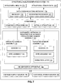
- FIG. 7 is an illustration of a block diagram of one of the embodiments of the structural health monitoring system 170 using the nanoparticle ink based piezoelectric sensors 110 of the disclosure.
- the system 170 comprises a structure 30 to be monitored for structural health 172.
- the system 170 further comprises a distributed network of nanoparticle ink based piezoelectric sensor assemblies 120 deposited onto a surface of the structure 30.
- the distributed network of nanoparticle ink based piezoelectric sensor assemblies 120 may be deposited onto a surface of the structure 30 with one or more layers of insulation, coatings, or paint in between a body 32 (see FIG. 5 ) of the structure 30 and the distributed network of nanoparticle ink based piezoelectric sensor assemblies 120.
- Each sensor assembly 120 comprises a plurality of nanoparticle ink based piezoelectric sensors 110.
- Each sensor assembly 120 further comprises a plurality of conductive ink power and communication wire assemblies 140, acting as actuator assemblies 141, interconnecting the plurality of nanoparticle ink based piezoelectric sensors 110.
- the structural health monitoring system 170 preferably comprises a deposited nanoparticle ink based piezoelectric sensor assembly 115 (see also FIGS. 2 and 3 ).
- the deposited nanoparticle ink based piezoelectric sensor assembly 115 may comprise a deposited nanoparticle ink based piezoelectric sensor assembly 116 (see FIG.
- the structural health monitoring system 170 further comprises an ink deposition apparatus 142 depositing the distributed network of nanoparticle ink based piezoelectric sensor assemblies 120 onto a surface of the structure 30.
- the structural health monitoring system 170 may further comprise a voltage supply source 176 for poling the plurality of sensors 110.
- the voltage supply source 176 may be used for poling the nanoparticle ink based piezoelectric sensors 110 prior to use in the structural health monitoring system 170.
- the term "poling” means a process by which a strong electric field is applied across a material, usually at elevated temperatures, in order to orient or align dipoles or domains.
- the voltage supply source 176 may also drive some piezoelectric sensors 110 so that they become actuators 141 sending interrogating signals to other piezoelectric sensors 110.
- the structural health monitoring system 170 further comprises an electrical power source 178 providing electrical power to the sensor assembly 120.
- the electrical power source 178 may comprise batteries, voltage, RFID (radio frequency identification), magnetic induction transmission, or another suitable electrical power source.
- the electrical power source 178 may be wireless.
- the structural health monitoring system 170 further comprises a data communications network 179 for retrieving and processing structural health data 174 of the structure 30 via one or more signals 92 from the sensors 110.
- the data communications network 179 may be wireless.
- the data communications network 179 may be digital or analog.
- the data communications network 179 may retrieve data received from the nanoparticle ink based piezoelectric sensors 110, such as with a receiver 175 (see FIG. 7 ), and may process data received from the nanoparticle ink based piezoelectric sensors 110, such as with a computer processor 177 (see FIG. 7 ).
- the data communications network 179 may be wireless.
- the deposition of the nanoparticle ink based piezoelectric sensors 110 onto a surface of the substrate 101 or onto a surface of the structure 30 (see FIG. 7 ) enables in situ installation of the nanoparticle ink based piezoelectric sensors 110 for applications such as structural health monitoring.
- the nanoparticle ink based piezoelectric sensors 110 may be a key enabler of high density structural health monitoring systems 170.
- Two or more nanoparticle ink based piezoelectric sensors 110 may be used to enable the structural health monitoring system 170 for monitoring structural health 172 of a structure 30, such as a composite structure 102 (see FIG. 1 ) or a metallic structure 132 (see FIG. 3 ), or another suitable structure, and for providing structural health data 174.
- the structural health data 174 may comprise disbonds, weak bonding, strain levels, moisture ingression, materials change, cracks, voids, delamination, porosity, or other suitable structural health data 174 or electromechanical properties or other irregularities which may adversely affect the performance of the structure 30.
- the structure 30 preferably comprises a material comprising a composite material, a metallic material, or a combination of a composite material and a metallic material.
- the structure 30 preferably has a curved surface 138 on which the distributed network of nanoparticle ink based piezoelectric sensor assemblies 120 is deposited.
- the nanoparticle ink based piezoelectric sensors 110 may be deposited onto the structure 30 in a customized shape 164 (see FIG. 6B ). As shown in FIG.
- the ink deposition apparatus 142 may comprise a direct write printing apparatus 144 comprising a jetted atomized deposition apparatus 146, an ink jet printing apparatus 147, an aerosol printing apparatus 190, a pulsed laser evaporation apparatus 192, a flexography printing apparatus 194, a micro-spray printing apparatus 196, a flat bed silk screen printing apparatus 197, a rotary silk screen printing apparatus 198, a gravure printing apparatus 199, or another suitable direct write printing apparatus 144.
- the distributed network of nanoparticle ink based piezoelectric sensor assemblies 120 may further comprise an insulation layer 134 deposited onto a surface of the structure 30. As shown in FIGS.
- the conductive ink power and communication wire assemblies 140 preferably comprise a first conductive electrode 114, a second conductive electrode 118, a first conductive trace wire 112a, and a second conductive trace wire 112b.
- the structural health data 174 may comprise disbonds, weak bonding, strain levels, moisture ingression, materials change, cracks, voids, delamination, porosity, and irregularities that adversely affect the performance of the structure 30.
- the nanoparticle ink based piezoelectric sensors 110 are preferably comprised of nanoparticles having a particle size in a range of from about 20 nanometers to about 1 micron.
- the structure 30 preferably comprises an aircraft structure 10 (see FIG. 1 ).
- FIG. 5 is an illustration of a block diagram of one of the embodiments of the structure 30 of the disclosure.
- the structure 30 comprises a body 32.
- the structure 30 further comprises a distributed network of nanoparticle ink based piezoelectric sensor assemblies 120 deposited onto a surface of the structure 30 via an ink deposition process 122.
- Each sensor assembly 120 comprises a plurality of nanoparticle ink based piezoelectric sensors 110.
- Each sensor assembly 120 further comprises a plurality of conductive ink actuator assemblies 141 interconnecting the plurality of nanoparticle ink based piezoelectric sensors 110.
- a signal path 90 within the sensor assembly 120 comprises a plurality of nanoparticles.
- Structural health data 174 (see FIG. 7 ) of the structure 30 is preferably obtained via one or more signals 92 from the nanoparticle ink based piezoelectric sensors 110 flowing through the signal path 90 to a data communications network 179 (see FIG. 7 ).
- the nanoparticle ink based piezoelectric sensors 110 may comprise a nanoparticle ink such as a formulated lead zirconate titanate (PZT) ink, barium titanate (BaTiO 3 ), or another suitable nanoparticle ink.
- the ink preferably comprises nanoscale ink nanoparticles.
- the nanoscale ink nanoparticles are pre-crystallized.
- the nanoparticle ink preferably has a nanoscale particle size in a range of from about 20 nanometers to about 1 micron.
- the nanoscale ink particles size allows for the nanoparticle ink to be deposited using a wide range of ink deposition processes, apparatuses, and systems, and in particular, allows for the nanoparticle ink to be deposited using a jetted atomized deposition process 126 (see FIGS. 6A and 9 ) and a jetted atomized deposition apparatus 146 (see FIGS. 6A and 9 ).
- Each of the nanoparticle ink based piezoelectric sensor 110 may have a thickness in a range of from about 1 micron to about 500 microns.
- the thickness of the nanoparticle ink based piezoelectric sensors 110 may be measured in terms of a factor of nanoparticle size of the nanoparticles and the thickness of first and second conductive electrodes 114, 118 (see FIG. 2 ). Thickness of the nanoparticle ink based piezoelectric sensor 110 may also depend on the size of the nanoparticle ink based piezoelectric sensor 110, as a proper aspect ratio may increase the sensitivity of the nanoparticle ink based piezoelectric sensor 110.
- the nanoparticle ink 104 may further comprise an adhesion promoter, such as a sol-gel based adhesion promoter, a polymer based adhesion promoter such as an epoxy or another suitable polymer based adhesion promoter, or another suitable adhesion promoter for promoting adhesion of the nanoparticle ink to a surface of the substrate 101 (see FIG. 5 ).
- an adhesion promoter such as a sol-gel based adhesion promoter, a polymer based adhesion promoter such as an epoxy or another suitable polymer based adhesion promoter, or another suitable adhesion promoter for promoting adhesion of the nanoparticle ink to a surface of the substrate 101 (see FIG. 5 ).
- the nanoscale ink nanoparticles may be suspended in a silica sol-gel and then deposited using an ink deposition process 122 such as a direct write printing process 124 (see FIG. 9 ).
- the silica sol-gel in the nanoparticle ink formulation enables the nanoparticle ink to bond to a wider variety of substrates than certain known adhesion promoters.
- the nanoparticle ink based piezoelectric sensor 110 preferably has modalities based on ultrasonic wave propagation and electromechanical impedance.
- PZT nanoparticle ink may be formulated by methods disclosed in contemporaneously filed U.S. nonprovisional patent application Serial Number 13/211,554 , titled “METHODS FOR FORMING LEAD ZIRCONATE TITANATE NANOPARTICLES", having Attorney Docket Number UWOTL-1-37259, filed on August 17, 2011, which is hereby incorporated by reference in its entirety.
- the substrate 101 may have a non-curved or planar surface 136, a curved or non-planar surface 138, or a combination of a non-curved or planar surface 136 and a curved or non-planar surface 138.
- the substrate 101 may have a first surface 103a and a second surface 103b.
- the substrate 101 preferably comprises a composite material, a metallic material, a combination of a composite material and a metallic material, or another suitable material.
- the substrate 101 may comprise a composite structure 102.
- the composite structure 102 may comprise composite materials such as polymeric composites, fiber-reinforced composite materials, fiber-reinforced polymers, carbon fiber reinforced plastics (CFRP), glass-reinforced plastics (GRP), thermoplastic composites, thermoset composites, epoxy resin composites, shape memory polymer composites, ceramic matrix composites, or another suitable composite material.
- the substrate 101 may comprise a metallic structure 132.
- the metallic structure 132 may comprise metal materials such as aluminum, stainless steel, titanium, alloys thereof, or another suitable metal or metal alloy.
- the substrate 101 may also comprise another suitable material.
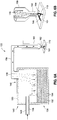
- FIG. 6A is an illustration of a schematic view of one of the embodiments of an ink deposition process 122 and an ink deposition apparatus 142 for fabricating the nanoparticle ink based piezoelectric sensors 110 of the disclosure.
- An exemplary direct write printing process 124 and direct write printing apparatus 144 are shown in FIG. 6A , which shows the jetted atomized deposition process 126 and the jetted atomized deposition apparatus 146.
- nanoscale ink nanoparticles 106 may be transferred via an inlet 148 into a mixing vessel 150 containing a solvent 152.
- the nanoscale ink nanoparticles 106 are preferably mixed with the solvent 152 in the mixing vessel to form a nanoparticle ink suspension 154.
- the nanoparticle ink suspension 154 may be atomized by an ultrasonic mechanism 158 to form atomized ink nanoparticles 156.
- the atomized ink nanoparticles 156 may then be transferred through a nozzle body 160 and directed through a nozzle tip 162 to the surface of the substrate 101 for depositing and printing of the nanoparticle ink based piezoelectric sensors 110 onto the substrate 101.
- FIG. 6B is an illustration of a close-up view of the piezoelectric nanoparticle ink based sensors 110 being deposited onto the surface of the substrate 101.
- FIG. 6B shows the atomized ink nanoparticles 156 in the nozzle body 160 and the nozzle tip 162 being deposited onto the substrate 101 to form the piezoelectric nanoparticle ink based sensors 110.
- the nanoparticle ink based piezoelectric sensors 110 may be deposited onto the substrate 101 in a customized shape 164, such as letters, designs, logos, or insignias, or geometric shapes, such as circles, squares, rectangles, triangles, or other geometric shapes, or another desired customized shape 164.
- the ink deposition process 122 and the ink deposition apparatus 142 do not require growth of crystals 166 on the substrate 101. Moreover, the deposited nanoscale ink nanoparticles 106 contain a crystalline particle structure that does not require any post processing steps to grow the crystals.
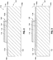
- FIGS. 2 and 3 show embodiments of a deposited nanoparticle ink based piezoelectric sensor assembly 115.
- FIG. 2 is an illustration of a cross-sectional view of one of the embodiments of a deposited nanoparticle ink based piezoelectric sensor assembly 116 that is deposited onto a substrate 101 comprising a composite structure 102.
- the deposited nanoparticle ink based piezoelectric sensor assembly 116 comprises the nanoparticle ink based piezoelectric sensor 110 coupled to a power and communication wire assembly 140 acting as an actuator assembly 141 (see FIG. 4 ).
- the power and communication wire assembly 140 is preferably formed of a conductive ink 168 (see FIG.
- the power and communication wire assembly 140 acting as an actuator assembly 141 may comprise a first conductive electrode 114, a second conductive electrode 118, a first conductive trace wire 112a, and a second conductive trace wire 112b.
- the first conductive electrode 114, the second conductive electrode 118, the first conductive trace wire 112a, and the second conductive trace wire 112b may be adjacent to the nanoparticle ink based piezoelectric sensor 110.
- FIG. 3 is an illustration of a cross-sectional view of another one of the embodiments of a deposited nanoparticle ink based piezoelectric sensor assembly 130 that is deposited onto a substrate 101 comprising a metallic structure 132.
- the deposited nanoparticle ink based piezoelectric sensor assembly 130 comprises the nanoparticle ink based piezoelectric sensor 110 coupled to a power and communication wire assembly 140 acting as an actuator assembly 141 (see FIG. 4 ).
- the power and communication wire assembly 140 is preferably formed of a conductive ink 168 (see FIG. 4 ) that may be deposited via the ink deposition apparatus 142 and via the ink deposition process 122 onto the substrate 101.
- the power and communication wire assembly 140 acting as an actuator assembly 141 may comprise the first conductive electrode 114, the second conductive electrode 118, the first conductive trace wire 112a, and the second conductive trace wire 112b.
- the first conductive electrode 114, the second conductive electrode 118, the first conductive trace wire 112a, and the second conductive trace wire 112b may be adjacent to the nanoparticle ink based piezoelectric sensor 110.
- the deposited nanoparticle ink based piezoelectric sensor assembly 130 further comprises an insulation layer 134 deposited directly onto the body of the substrate 101, the substrate 101 comprising the metallic structure 132.
- the nanoparticle ink based piezoelectric sensor 110 may be deposited over the insulation layer 134.
- the insulation layer 134 may comprise an insulating polymer coating, a dielectric material, a ceramic material, a polymer material, or another suitable insulation material.
- the nanoparticle ink based piezoelectric sensor 110 is preferably coupled to the power and communication wire assembly 140.
- FIG. 4 is an illustration of a top perspective view of the distributed network of nanoparticle ink based piezoelectric sensor assemblies 120.
- FIG. 4 shows a plurality of the nanoparticle ink based piezoelectric sensors 110 coupled to the plurality of conductive ink 168 power and communication wire assemblies 140 acting as actuator assemblies 141, all deposited on the structure 30, such as the composite structure 102.
- a plurality of nanoparticle ink based piezoelectric sensors 110 may be coupled to a plurality of power and communication wire assemblies 140, all deposited on the metallic structure 132.
- FIG. 8 is an illustration of a flow diagram of an embodiment of the method 200 of the disclosure.
- the method 200 comprises step 202 of providing a structure 30 to be monitored for structural health 172 (see FIG. 7 ).
- the method 200 further comprises step 204 of depositing onto the structure 30 via an ink deposition process 122 a plurality of nanoparticle ink based piezoelectric sensors 110 and a plurality of conductive ink power and communication wire assemblies 140 interconnecting the plurality of sensors 110 to form a distributed network of nanoparticle ink based piezoelectric sensor assemblies 120.
- the method 200 further comprises optional step 206 of poling the nanoparticle ink based piezoelectric sensors 110 with a voltage supply source 176 (see FIG. 7 ) to create an electric field across the nanoparticle ink based piezoelectric sensors 110.
- the method 200 further comprises step 208 of providing electrical power to the distributed network of nanoparticle ink based piezoelectric sensor assemblies 120 via an electrical power source 178 (see FIG. 7 ).
- the method 200 further comprises step 210 of using a data communications network 179 (see FIG. 7 ) to retrieve and process structural health data 174 (see FIG. 7 ) of the structure 30 via one or more signals 92 (see FIG. 5 ) from the nanoparticle ink based piezoelectric sensors 110.
- the structure 30 preferably comprises an aircraft structure 10 (see FIG. 1 ).
- the ink deposition process 122 may comprise a direct write printing process 124 comprising a jetted atomized deposition process 126, an ink jet printing process 128, an aerosol printing process 180, a pulsed laser evaporation process 182, a flexography printing process 184, a micro-spray printing process 186, a flat bed silk screen printing process 187, a rotary silk screen printing process 188, a gravure printing process 189, or another suitable direct write printing process 124.
- the data communications network 179 may retrieve structural health data 174 received from the nanoparticle ink based piezoelectric sensors 110 with a receiver 175 (see FIG.
- the structural health data 174 may comprise disbonds, weak bonding, strain levels, moisture ingression, materials change, cracks, voids, delamination, porosity, and irregularities that adversely affect the performance of the structure, or other suitable structural health data 174.
- the substrate 101 preferably comprises a composite material, a metallic material, a combination of a composite material and a metallic material, or another suitable material.
- the substrate 101 preferably comprises a first surface 103a and a second surface 103b (see FIG. 2 ).
- the substrate 101 may have a non-curved or planar surface 136 (see FIG. 5 ), a curved or non-planar surface 138 (see FIG. 5 ), or a combination of a non-curved or planar surface 136 (see FIG. 5 ) and a curved or non-planar surface 138 (see FIG. 5 ).
- the nanoparticle ink based piezoelectric sensors 110 may be deposited onto the substrate 101 in a customized shape 164 (see FIG. 6B ).
- the nanoparticle ink based piezoelectric sensors 110 may undergo a poling process with a voltage supply source 176 (see FIG. 7 ) prior to being used in the structural health monitoring system 170 for monitoring structural health 172 of the structure 30.
- the nanoparticle ink based piezoelectric sensors 110 may be coupled to the power and communication wire assembly 140 formed from a conductive ink 168 deposited onto the substrate 101 via the ink deposition process 122 prior to being used in the structural health monitoring system 170. Two or more nanoparticle ink based piezoelectric sensors 110 may be used to enable the structural health monitoring system 170.
- the structure 30 may comprise an aircraft 10 (see FIG. 1 ), a spacecraft, an aerospace vehicle, a space launch vehicle, a rocket, a satellite, a rotorcraft, a watercraft, a boat, a train, an automobile, a truck, a bus, an architectural structure, a turbine blade, a medical device, electronic actuation equipment, a consumer electronic device, vibratory equipment, passive and active dampers, or another suitable structure.
- the system 170 and method 200 may be used across many industries including, for example, wind power generation (health monitoring of turbine blades), aerospace applications, military applications, medical applications, electronic actuation equipment, consumer electronic products, or any application where structures or materials require a monitoring system.
- a method of monitoring structural health 172 of a structure 30 comprises providing a structure 30 to be monitored for structural health 172.
- the method further comprises using a distributed network of nanoparticle ink based piezoelectric sensor assemblies 120 to sense and monitor the structural health 172 of the structure 30.
- the method further comprises providing electrical power to the distributed network of sensor assemblies 120 via an electrical power source 178.
- the method further comprises using a data communications network 179 to retrieve and process structural health data 174 of the structure 30 via one or more signals from the nanoparticle ink based piezoelectric sensor assemblies 120.
- Embodiments of the system 170 and method 200 disclosed herein provide nanoparticle ink based piezoelectric sensors 110 for structural health monitoring that may be used for a variety of applications including ultrasonic damage detection for composite and metallic structures, crack propagation detection sensors, pressure sensors, or another suitable sensor.
- the nanoparticle ink based piezoelectric sensors 110 of the system 170 and method 200 may provide cradle to grave health monitoring of various components in aircraft such as damage detection for door surrounds, military platforms such as crack growth detection for military aircraft, and space systems such as cryo-tank health monitoring.
- the nanoparticle ink based piezoelectric sensors 110 may provide structural health data that was previously not available that may influence new and efficient designs which may reduce costs.
- the jetted atomized deposition process 126 along with the formulated nanoparticle ink, allows many nanoparticle ink based piezoelectric sensors 110 to be deposited onto a surface of a substrate 101 or a surface of a structure 30 and at a decreased cost as compared to known processes of depositing piezeoelectric sensors.
- Embodiments of the system 170 and method 200 disclosed herein provide nanoparticle ink based piezoelectric sensors 110 that allow for the placement of the nanoparticle ink based piezoelectric sensors 110 in numerous areas of the structure 30 and in large quantities, both of which may be difficult with known piezoelectric sensors.
- embodiments of the system 170 and method 200 disclosed herein provide nanoparticle ink based piezoelectric sensors 110 that are advantageous over known sensors because they may not require an adhesive to bond them to the substrate or structure, and this decreases the possibility that the nanoparticle ink based piezoelectric sensors 110 may disbond from the structure 30. Further, embodiments of the system 170 and method 200 disclosed herein provide nanoparticle ink based piezoelectric sensors 110 that are enabled by the availability of nanoscale ink particles 106 having favorable piezoelectric properties and that are deposited onto a substrate or structure in a desired configuration for use without the use of adhesive.
- nanoparticle ink based piezoelectric sensors 110 may be deposited onto a substrate or structure with no adhesive between the sensors 110 and the substrate or structure, improved signal coupling into the structure being interrogated may be achieved. Further, embodiments of the system 170 and method 200 disclosed herein provide nanoparticle ink based piezoelectric sensors 110 that do not require manual placement or installation on the substrate or structure and may be deposited or printed onto the substrate or structure, along with all the required power and communication wire assemblies, thus decreasing labor and installation costs, as well as decreasing complexity and weight of the structure.
- the nanoparticle ink based piezoelectric sensors 110 may be deposited with numerous direct write printing processes, including the jetted atomized deposition process 126; may be fabricated from nanoparticle size particles which have been pre-crystallized and may be more efficient than known sensors that have not been crystallized; do not require a high temperature sintering/crystallization process and thus reduces or eliminates possible damage to temperature sensitive substrates or structures; may be deposited onto curved or non-planar substrates or structures; have no or minimal physical geometry limitations and thus decreases the possibility of inadequate sensing capacities or inadequate actuation responses.
- numerous direct write printing processes including the jetted atomized deposition process 126; may be fabricated from nanoparticle size particles which have been pre-crystallized and may be more efficient than known sensors that have not been crystallized; do not require a high temperature sintering/crystallization process and thus reduces or eliminates possible damage to temperature sensitive substrates or structures; may be deposited onto curved or non-planar substrates or structures
- embodiments of the system 170 and method 200 disclosed herein provide nanoparticle ink based piezoelectric sensors 110 that may be used to predict deterioration or weaknesses of the structure 30 prior to the actual development of such deterioration or weaknesses, and thus, may increase reliability of the structure or structural component parts, and may reduce overall manufacturing and maintenance costs over the life of the structure or structural component parts.
- embodiments of the system 170 and method 200 disclosed herein have the ability to predict, monitor, and diagnose the integrity, health, and fitness of a structure without having to disassemble or remove the structure or drill holes into the structure for insertion of any measurement tools.
- a system for monitoring structural health 172 of a structure 30, the system including a structure 30 to be monitored for structural health 172; a distributed network of nanoparticle ink based piezoelectric sensor assemblies 120 deposited onto the structure 30, each assembly including a plurality of nanoparticle ink based piezoelectric sensors 110 ; and, a plurality of conductive ink power and communication wire assemblies 140 interconnecting the plurality of sensors 110; an ink deposition apparatus 142 depositing the distributed network of nanoparticle ink based piezoelectric sensor assemblies 120 onto the structure 30; an electrical power source 178 providing electrical power to the distributed network; and, a data communications network 179 retrieving and processing structural health data 174 of the structure 30 via one or more signals from the sensors 110.
- the system includes a voltage supply source 176 poling the plurality of nanoparticle ink based piezoelectric sensors 110.
- the structure 30 comprises a material selected from a group comprising a composite material, a metallic material, and a combination of a composite material and a metallic material.
- the structure 30 has a curved surface on which the distributed network of nanoparticle ink based piezoelectric sensor assemblies 120 is deposited.
- the nanoparticle ink based piezoelectric sensors 110 are deposited onto the structure in a customized shape.
- the ink deposition apparatus 142 includes a direct write printing apparatus selected from a group comprising a jetted atomized deposition apparatus, an ink jet printing apparatus, an aerosol printing apparatus, a pulsed laser evaporation apparatus, a flexography printing apparatus, a micro-spray printing apparatus, a flat bed silk screen printing apparatus, a rotary silk screen printing process, and a gravure printing process.
- a direct write printing apparatus selected from a group comprising a jetted atomized deposition apparatus, an ink jet printing apparatus, an aerosol printing apparatus, a pulsed laser evaporation apparatus, a flexography printing apparatus, a micro-spray printing apparatus, a flat bed silk screen printing apparatus, a rotary silk screen printing process, and a gravure printing process.
- the distributed network of nanoparticle ink based piezoelectric sensor assemblies 120 further includes an insulation layer deposited onto a body of the structure 30.
- each of the conductive ink power and communication wire assemblies 140 includes a first conductive electrode 114, a second conductive electrode 118, a first conductive trace wire, and a second conductive trace wire.
- the structural health data 174 includes disbonds, weak bonding, strain levels, moisture ingression, materials change, cracks, voids, delamination, porosity, and irregularities that adversely affect performance of the structure 30.
- the nanoparticle ink based piezoelectric sensors 110 are comprised of nanoparticles having a particle size in a range of from about 20 nanometers to about 1 micron.
- the structure 30 includes an aircraft structure.
- a method is disclosed of monitoring structural health 172 of a structure 30, the method including providing a structure to be monitored for structural health 172; depositing onto the structure 30 via an ink deposition process a plurality of nanoparticle ink based piezoelectric sensors 110 and a plurality of conductive ink power and communication wire assemblies 140 interconnecting the plurality of sensors to form a distributed network of nanoparticle ink based piezoelectric sensor assemblies 120; providing electrical power to the distributed network via an electrical power source 178; and using a data communications network 179 to retrieve and process structural health data of the structure 30 via one or more signals from the sensors 110.
- the method further includes after depositing the plurality of nanoparticle ink based piezoelectric sensors 110, poling the nanoparticle ink based piezoelectric sensors 110 with a voltage supply source 176 to create an electric field across the nanoparticle ink based piezoelectric sensors 110.
- the ink deposition process comprises a direct write printing process selected from a group comprising a jetted atomized deposition process, an ink jet printing process, an aerosol printing process, a pulsed laser evaporation process, a flexography printing process, a micro-spray printing process, a flat bed silk screen printing process, a rotary silk screen printing process, and a gravure printing process.
- the data communications network 179 retrieves data received from the nanoparticle ink based piezoelectric sensors 110 with a receiver and processes data received from the nanoparticle ink based piezoelectric sensors 110 with a computer processor.
- the structural health data 174 comprises disbonds, weak bonding, strain levels, moisture ingression, materials change, cracks, voids, delamination, porosity, and irregularities that adversely affect performance of the structure.
- a structure 30 is disclosed to be monitored for structural health, the structure including a body; and a distributed network of nanoparticle ink based piezoelectric sensor assemblies 120 deposited onto the body of the structure 30 via an ink deposition process, each assembly including a plurality of nanoparticle ink based piezoelectric sensors 110; and a plurality of conductive ink actuator assemblies 141 interconnecting the plurality of sensors 110, wherein a signal path within the distributed network 120 comprises a plurality of nanoparticles and structural health data 174 of the structure 30 is obtained via one or more signals from the nanoparticle ink based piezoelectric sensors 110 flowing through the signal path to a data communications network 179.
- the structure 30 has a curved surface on which the distributed network of nanoparticle ink based piezoelectric sensor assemblies 120 is deposited.
- the distributed network of nanoparticle ink based piezoelectric sensor assemblies 120 further includes an insulation layer deposited onto the body.
- the nanoparticle ink based piezoelectric sensors 110 are comprised of nanoparticles having a particle size in a range of from about 20 nanometers to about 1 micron.
- the ink deposition process comprises a direct write printing process selected from a group comprising a jetted atomized deposition process, an ink jet printing process, an aerosol printing process, a pulsed laser evaporation process, a flexography printing process, a micro-spray printing process, a flat bed silk screen printing process, a rotary silk screen printing process, and a gravure printing process.
- the structure 30 comprises an aircraft structure.
Landscapes
- Engineering & Computer Science (AREA)
- Physics & Mathematics (AREA)
- General Physics & Mathematics (AREA)
- Chemical & Material Sciences (AREA)
- Nanotechnology (AREA)
- Aviation & Aerospace Engineering (AREA)
- Analytical Chemistry (AREA)
- Immunology (AREA)
- Crystallography & Structural Chemistry (AREA)
- Condensed Matter Physics & Semiconductors (AREA)
- Health & Medical Sciences (AREA)
- Life Sciences & Earth Sciences (AREA)
- Composite Materials (AREA)
- Biochemistry (AREA)
- General Health & Medical Sciences (AREA)
- Materials Engineering (AREA)
- Pathology (AREA)
- Manufacturing & Machinery (AREA)
- Testing Of Devices, Machine Parts, Or Other Structures Thereof (AREA)
- Inks, Pencil-Leads, Or Crayons (AREA)
- Arrangements For Transmission Of Measured Signals (AREA)
- Formation Of Insulating Films (AREA)
- Ink Jet (AREA)
- Application Of Or Painting With Fluid Materials (AREA)
Applications Claiming Priority (1)
| Application Number | Priority Date | Filing Date | Title |
|---|---|---|---|
| US13/212,123 US8766511B2 (en) | 2011-08-17 | 2011-08-17 | Method and system for distributed network of nanoparticle ink based piezoelectric sensors for structural health monitoring |
Publications (2)
| Publication Number | Publication Date |
|---|---|
| EP2559656A1 EP2559656A1 (en) | 2013-02-20 |
| EP2559656B1 true EP2559656B1 (en) | 2021-01-20 |
Family
ID=47010168
Family Applications (1)
| Application Number | Title | Priority Date | Filing Date |
|---|---|---|---|
| EP12175708.2A Active EP2559656B1 (en) | 2011-08-17 | 2012-07-10 | Method and system for distributed network of nanoparticle ink based piezoelectric sensors for structural health monitoring |
Country Status (5)
| Country | Link |
|---|---|
| US (1) | US8766511B2 (enExample) |
| EP (1) | EP2559656B1 (enExample) |
| JP (2) | JP6084395B2 (enExample) |
| CN (1) | CN102954893B (enExample) |
| CA (1) | CA2785400C (enExample) |
Families Citing this family (27)
| Publication number | Priority date | Publication date | Assignee | Title |
|---|---|---|---|---|
| US8886388B2 (en) * | 2009-06-29 | 2014-11-11 | The Boeing Company | Embedded damage detection system for composite materials of an aircraft |
| US9005465B2 (en) | 2011-08-17 | 2015-04-14 | University Of Washington Through Its Center For Commercialization | Methods for forming lead zirconate titanate nanoparticles |
| US10118712B2 (en) * | 2011-08-17 | 2018-11-06 | The Boeing Company | Electrical conductor pathway system and method of making the same |
| US8614724B2 (en) * | 2011-08-17 | 2013-12-24 | The Boeing Company | Method and system of fabricating PZT nanoparticle ink based piezoelectric sensor |
| FR2999715B1 (fr) * | 2012-12-18 | 2015-01-16 | Airbus Operations Sas | Dispositif et procede de detection d'un impact sur une structure en materiau composite. |
| US8878700B2 (en) | 2013-02-18 | 2014-11-04 | The Boeing Company | Aircraft monitoring system |
| US9656220B2 (en) * | 2014-02-17 | 2017-05-23 | The Boeing Company | Method and apparatus for atomizing a deposition mixture |
| CN104062446B (zh) * | 2014-06-16 | 2016-03-09 | 中国飞机强度研究所 | 一种飞机结构健康监测集成系统及方法 |
| US9354621B2 (en) | 2014-06-16 | 2016-05-31 | General Electric Company | Systems and methods for control of an adaptive-cycle engine with power-thermal management system |
| US9446864B2 (en) | 2014-10-17 | 2016-09-20 | The Boeing Company | NANOSAT electrothermal deployment system |
| WO2016144972A1 (en) * | 2015-03-09 | 2016-09-15 | Micromem Applied Sensor Technologies Inc. | Cement integrity sensors and methods of manufacture and use thereof |
| CN108291796B (zh) * | 2015-11-13 | 2020-04-24 | 株式会社村田制作所 | 压电挠曲传感器以及检测装置 |
| CN106741993A (zh) * | 2015-11-23 | 2017-05-31 | 中航贵州飞机有限责任公司 | 飞机健康监测与管理系统 |
| IL247408B (en) | 2016-08-21 | 2018-03-29 | Elbit Systems Ltd | A system and method for identifying weaknesses in the adhesion between structural elements |
| JP6374608B1 (ja) * | 2016-09-26 | 2018-08-15 | 株式会社Subaru | 損傷検知システム及び損傷検知方法 |
| EP3336485B1 (en) | 2016-12-15 | 2020-09-23 | Safran Landing Systems UK Limited | Aircraft assembly including deflection sensor |
| DE102017106403A1 (de) | 2017-03-24 | 2018-09-27 | Fresenius Medical Care Deutschland Gmbh | Medizinische Einrichtung mit additiv aufgebrachtem Wandler samt Leiterbahn |
| DE102017106404A1 (de) | 2017-03-24 | 2018-09-27 | Fresenius Medical Care Deutschland Gmbh | Einrichtung mit Einrichtung zum Ermitteln einer, insbesondere geometrischen, Eigenschaft der Einrichtung |
| DE102017106402A1 (de) | 2017-03-24 | 2018-09-27 | Fresenius Medical Care Deutschland Gmbh | Medizinische Einrichtung mit additiv aufgebrachtem Wandler |
| CN108146615A (zh) * | 2017-12-07 | 2018-06-12 | 南京航空航天大学 | 飞行器机电一体化大面积柔性冲击监测智能蒙皮系统 |
| SG11202013146XA (en) * | 2018-07-30 | 2021-01-28 | Agency Science Tech & Res | Structural health monitoring method and system |
| US11371913B2 (en) * | 2018-09-17 | 2022-06-28 | Board Of Supervisors Of Louisiana State University | Methods and devices for sample capture using gas-pulse nanoparticle displacement |
| CN109798941A (zh) * | 2019-03-14 | 2019-05-24 | 上海交通大学 | Cfrp模压成形及cfrp/金属复合板材单步共固化成形测试装置 |
| SG11202108828SA (en) * | 2019-03-20 | 2021-09-29 | Agency Science Tech & Res | Structural health monitoring method and system |
| DE102019111042A1 (de) * | 2019-04-29 | 2020-10-29 | Airbus Operations Gmbh | Strukturüberwachungssystem und Strukturüberwachungsverfahren |
| US11745440B2 (en) | 2020-04-03 | 2023-09-05 | The Boeing Company | Automated lamination system and method for embedding printed electronic elements in a composite structure |
| CN114411942A (zh) * | 2022-03-01 | 2022-04-29 | 江苏领跑梦毛勒智造科技集团有限公司 | 一种全预制装配式建筑 |
Family Cites Families (13)
| Publication number | Priority date | Publication date | Assignee | Title |
|---|---|---|---|---|
| US6006163A (en) * | 1997-09-15 | 1999-12-21 | Mcdonnell Douglas Corporation | Active damage interrogation method for structural health monitoring |
| US6370964B1 (en) * | 1998-11-23 | 2002-04-16 | The Board Of Trustees Of The Leland Stanford Junior University | Diagnostic layer and methods for detecting structural integrity of composite and metallic materials |
| JP3508682B2 (ja) * | 1999-03-02 | 2004-03-22 | セイコーエプソン株式会社 | 圧電アクチュエータ、インクジェット式記録ヘッド、これらの製造方法及びインクジェットプリンタ |
| JP4590493B2 (ja) * | 2003-07-31 | 2010-12-01 | 独立行政法人産業技術総合研究所 | 立体構造物の製造方法 |
| US7148803B2 (en) * | 2003-10-24 | 2006-12-12 | Symbol Technologies, Inc. | Radio frequency identification (RFID) based sensor networks |
| WO2005069858A2 (en) * | 2004-01-16 | 2005-08-04 | Northern Illinois University | Nano-composite piezoelectric material |
| US20060004499A1 (en) * | 2004-06-30 | 2006-01-05 | Angela Trego | Structural health management architecture using sensor technology |
| US7483805B2 (en) * | 2006-12-26 | 2009-01-27 | Integrated Sensing Systems, Inc. | Sensing and analysis system, network, and method |
| JP4984943B2 (ja) * | 2007-02-13 | 2012-07-25 | 富士通株式会社 | 圧電センサ装置及び記録装置 |
| US8447530B2 (en) * | 2008-01-11 | 2013-05-21 | The Boeing Company | High density structural health monitoring system and method |
| US8047049B2 (en) * | 2009-01-19 | 2011-11-01 | Palo Alto Research Center Incorporated | Conformal sensor tape |
| US8519449B2 (en) * | 2009-08-25 | 2013-08-27 | Honeywell International Inc. | Thin-film transistor based piezoelectric strain sensor and method |
| EP2489442A1 (en) * | 2011-02-18 | 2012-08-22 | Aernnova Engineering Solutions Iberica | Integrated phased array transducer, system and methodology for structural health monitoring of aerospace structures |
-
2011
- 2011-08-17 US US13/212,123 patent/US8766511B2/en active Active
-
2012
- 2012-07-10 EP EP12175708.2A patent/EP2559656B1/en active Active
- 2012-08-13 CA CA2785400A patent/CA2785400C/en active Active
- 2012-08-16 JP JP2012180371A patent/JP6084395B2/ja active Active
- 2012-08-17 CN CN201210295064.XA patent/CN102954893B/zh active Active
-
2017
- 2017-01-25 JP JP2017010851A patent/JP6400133B2/ja active Active
Non-Patent Citations (1)
| Title |
|---|
| None * |
Also Published As
| Publication number | Publication date |
|---|---|
| JP6084395B2 (ja) | 2017-02-22 |
| US8766511B2 (en) | 2014-07-01 |
| JP6400133B2 (ja) | 2018-10-03 |
| CA2785400C (en) | 2015-10-06 |
| CN102954893A (zh) | 2013-03-06 |
| CN102954893B (zh) | 2017-10-31 |
| US20130044155A1 (en) | 2013-02-21 |
| CA2785400A1 (en) | 2013-02-17 |
| JP2013051413A (ja) | 2013-03-14 |
| EP2559656A1 (en) | 2013-02-20 |
| JP2017096975A (ja) | 2017-06-01 |
Similar Documents
| Publication | Publication Date | Title |
|---|---|---|
| EP2559656B1 (en) | Method and system for distributed network of nanoparticle ink based piezoelectric sensors for structural health monitoring | |
| CA2783416C (en) | Method and system of fabricating pzt nanoparticle ink based piezoelectric sensor | |
| US10118712B2 (en) | Electrical conductor pathway system and method of making the same | |
| US11654613B2 (en) | Printed multifunctional skin for aerodynamic structures, and associated systems and methods | |
| CN103502802B (zh) | 监测粘合完整性的系统和方法 | |
| US11477888B2 (en) | Printed multifunctional skin for aerodynamic structures and associated systems and methods | |
| BR102017006351A2 (pt) | Electrical conduction path system and method of manufacturing the same |
Legal Events
| Date | Code | Title | Description |
|---|---|---|---|
| PUAI | Public reference made under article 153(3) epc to a published international application that has entered the european phase |
Free format text: ORIGINAL CODE: 0009012 |
|
| AK | Designated contracting states |
Kind code of ref document: A1 Designated state(s): AL AT BE BG CH CY CZ DE DK EE ES FI FR GB GR HR HU IE IS IT LI LT LU LV MC MK MT NL NO PL PT RO RS SE SI SK SM TR |
|
| AX | Request for extension of the european patent |
Extension state: BA ME |
|
| 17P | Request for examination filed |
Effective date: 20130807 |
|
| RBV | Designated contracting states (corrected) |
Designated state(s): AL AT BE BG CH CY CZ DE DK EE ES FI FR GB GR HR HU IE IS IT LI LT LU LV MC MK MT NL NO PL PT RO RS SE SI SK SM TR |
|
| 17Q | First examination report despatched |
Effective date: 20151027 |
|
| RIC1 | Information provided on ipc code assigned before grant |
Ipc: C08K 3/04 20060101ALI20180413BHEP Ipc: H01L 41/314 20130101ALI20180413BHEP Ipc: G01N 29/24 20060101ALI20180413BHEP Ipc: H01L 41/113 20060101ALI20180413BHEP Ipc: B82Y 30/00 20110101AFI20180413BHEP Ipc: G01M 5/00 20060101ALI20180413BHEP |
|
| GRAP | Despatch of communication of intention to grant a patent |
Free format text: ORIGINAL CODE: EPIDOSNIGR1 |
|
| STAA | Information on the status of an ep patent application or granted ep patent |
Free format text: STATUS: GRANT OF PATENT IS INTENDED |
|
| INTG | Intention to grant announced |
Effective date: 20180528 |
|
| GRAJ | Information related to disapproval of communication of intention to grant by the applicant or resumption of examination proceedings by the epo deleted |
Free format text: ORIGINAL CODE: EPIDOSDIGR1 |
|
| STAA | Information on the status of an ep patent application or granted ep patent |
Free format text: STATUS: EXAMINATION IS IN PROGRESS |
|
| INTC | Intention to grant announced (deleted) | ||
| GRAP | Despatch of communication of intention to grant a patent |
Free format text: ORIGINAL CODE: EPIDOSNIGR1 |
|
| STAA | Information on the status of an ep patent application or granted ep patent |
Free format text: STATUS: GRANT OF PATENT IS INTENDED |
|
| INTG | Intention to grant announced |
Effective date: 20200804 |
|
| GRAS | Grant fee paid |
Free format text: ORIGINAL CODE: EPIDOSNIGR3 |
|
| GRAA | (expected) grant |
Free format text: ORIGINAL CODE: 0009210 |
|
| STAA | Information on the status of an ep patent application or granted ep patent |
Free format text: STATUS: THE PATENT HAS BEEN GRANTED |
|
| AK | Designated contracting states |
Kind code of ref document: B1 Designated state(s): AL AT BE BG CH CY CZ DE DK EE ES FI FR GB GR HR HU IE IS IT LI LT LU LV MC MK MT NL NO PL PT RO RS SE SI SK SM TR |
|
| REG | Reference to a national code |
Ref country code: GB Ref legal event code: FG4D |
|
| REG | Reference to a national code |
Ref country code: CH Ref legal event code: EP |
|
| REG | Reference to a national code |
Ref country code: DE Ref legal event code: R096 Ref document number: 602012074193 Country of ref document: DE |
|
| REG | Reference to a national code |
Ref country code: AT Ref legal event code: REF Ref document number: 1356234 Country of ref document: AT Kind code of ref document: T Effective date: 20210215 |
|
| REG | Reference to a national code |
Ref country code: IE Ref legal event code: FG4D |
|
| REG | Reference to a national code |
Ref country code: NL Ref legal event code: MP Effective date: 20210120 |
|
| REG | Reference to a national code |
Ref country code: LT Ref legal event code: MG9D |
|
| REG | Reference to a national code |
Ref country code: AT Ref legal event code: MK05 Ref document number: 1356234 Country of ref document: AT Kind code of ref document: T Effective date: 20210120 |
|
| PG25 | Lapsed in a contracting state [announced via postgrant information from national office to epo] |
Ref country code: GR Free format text: LAPSE BECAUSE OF FAILURE TO SUBMIT A TRANSLATION OF THE DESCRIPTION OR TO PAY THE FEE WITHIN THE PRESCRIBED TIME-LIMIT Effective date: 20210421 Ref country code: HR Free format text: LAPSE BECAUSE OF FAILURE TO SUBMIT A TRANSLATION OF THE DESCRIPTION OR TO PAY THE FEE WITHIN THE PRESCRIBED TIME-LIMIT Effective date: 20210120 Ref country code: FI Free format text: LAPSE BECAUSE OF FAILURE TO SUBMIT A TRANSLATION OF THE DESCRIPTION OR TO PAY THE FEE WITHIN THE PRESCRIBED TIME-LIMIT Effective date: 20210120 Ref country code: PT Free format text: LAPSE BECAUSE OF FAILURE TO SUBMIT A TRANSLATION OF THE DESCRIPTION OR TO PAY THE FEE WITHIN THE PRESCRIBED TIME-LIMIT Effective date: 20210520 Ref country code: LT Free format text: LAPSE BECAUSE OF FAILURE TO SUBMIT A TRANSLATION OF THE DESCRIPTION OR TO PAY THE FEE WITHIN THE PRESCRIBED TIME-LIMIT Effective date: 20210120 Ref country code: NL Free format text: LAPSE BECAUSE OF FAILURE TO SUBMIT A TRANSLATION OF THE DESCRIPTION OR TO PAY THE FEE WITHIN THE PRESCRIBED TIME-LIMIT Effective date: 20210120 Ref country code: NO Free format text: LAPSE BECAUSE OF FAILURE TO SUBMIT A TRANSLATION OF THE DESCRIPTION OR TO PAY THE FEE WITHIN THE PRESCRIBED TIME-LIMIT Effective date: 20210420 Ref country code: BG Free format text: LAPSE BECAUSE OF FAILURE TO SUBMIT A TRANSLATION OF THE DESCRIPTION OR TO PAY THE FEE WITHIN THE PRESCRIBED TIME-LIMIT Effective date: 20210420 |
|
| PG25 | Lapsed in a contracting state [announced via postgrant information from national office to epo] |
Ref country code: SE Free format text: LAPSE BECAUSE OF FAILURE TO SUBMIT A TRANSLATION OF THE DESCRIPTION OR TO PAY THE FEE WITHIN THE PRESCRIBED TIME-LIMIT Effective date: 20210120 Ref country code: RS Free format text: LAPSE BECAUSE OF FAILURE TO SUBMIT A TRANSLATION OF THE DESCRIPTION OR TO PAY THE FEE WITHIN THE PRESCRIBED TIME-LIMIT Effective date: 20210120 Ref country code: LV Free format text: LAPSE BECAUSE OF FAILURE TO SUBMIT A TRANSLATION OF THE DESCRIPTION OR TO PAY THE FEE WITHIN THE PRESCRIBED TIME-LIMIT Effective date: 20210120 Ref country code: PL Free format text: LAPSE BECAUSE OF FAILURE TO SUBMIT A TRANSLATION OF THE DESCRIPTION OR TO PAY THE FEE WITHIN THE PRESCRIBED TIME-LIMIT Effective date: 20210120 Ref country code: AT Free format text: LAPSE BECAUSE OF FAILURE TO SUBMIT A TRANSLATION OF THE DESCRIPTION OR TO PAY THE FEE WITHIN THE PRESCRIBED TIME-LIMIT Effective date: 20210120 |
|
| PG25 | Lapsed in a contracting state [announced via postgrant information from national office to epo] |
Ref country code: IS Free format text: LAPSE BECAUSE OF FAILURE TO SUBMIT A TRANSLATION OF THE DESCRIPTION OR TO PAY THE FEE WITHIN THE PRESCRIBED TIME-LIMIT Effective date: 20210520 |
|
| REG | Reference to a national code |
Ref country code: DE Ref legal event code: R097 Ref document number: 602012074193 Country of ref document: DE |
|
| PG25 | Lapsed in a contracting state [announced via postgrant information from national office to epo] |
Ref country code: SM Free format text: LAPSE BECAUSE OF FAILURE TO SUBMIT A TRANSLATION OF THE DESCRIPTION OR TO PAY THE FEE WITHIN THE PRESCRIBED TIME-LIMIT Effective date: 20210120 Ref country code: EE Free format text: LAPSE BECAUSE OF FAILURE TO SUBMIT A TRANSLATION OF THE DESCRIPTION OR TO PAY THE FEE WITHIN THE PRESCRIBED TIME-LIMIT Effective date: 20210120 Ref country code: CZ Free format text: LAPSE BECAUSE OF FAILURE TO SUBMIT A TRANSLATION OF THE DESCRIPTION OR TO PAY THE FEE WITHIN THE PRESCRIBED TIME-LIMIT Effective date: 20210120 |
|
| PLBE | No opposition filed within time limit |
Free format text: ORIGINAL CODE: 0009261 |
|
| STAA | Information on the status of an ep patent application or granted ep patent |
Free format text: STATUS: NO OPPOSITION FILED WITHIN TIME LIMIT |
|
| PG25 | Lapsed in a contracting state [announced via postgrant information from national office to epo] |
Ref country code: RO Free format text: LAPSE BECAUSE OF FAILURE TO SUBMIT A TRANSLATION OF THE DESCRIPTION OR TO PAY THE FEE WITHIN THE PRESCRIBED TIME-LIMIT Effective date: 20210120 Ref country code: DK Free format text: LAPSE BECAUSE OF FAILURE TO SUBMIT A TRANSLATION OF THE DESCRIPTION OR TO PAY THE FEE WITHIN THE PRESCRIBED TIME-LIMIT Effective date: 20210120 Ref country code: ES Free format text: LAPSE BECAUSE OF FAILURE TO SUBMIT A TRANSLATION OF THE DESCRIPTION OR TO PAY THE FEE WITHIN THE PRESCRIBED TIME-LIMIT Effective date: 20210120 Ref country code: SK Free format text: LAPSE BECAUSE OF FAILURE TO SUBMIT A TRANSLATION OF THE DESCRIPTION OR TO PAY THE FEE WITHIN THE PRESCRIBED TIME-LIMIT Effective date: 20210120 |
|
| 26N | No opposition filed |
Effective date: 20211021 |
|
| PG25 | Lapsed in a contracting state [announced via postgrant information from national office to epo] |
Ref country code: AL Free format text: LAPSE BECAUSE OF FAILURE TO SUBMIT A TRANSLATION OF THE DESCRIPTION OR TO PAY THE FEE WITHIN THE PRESCRIBED TIME-LIMIT Effective date: 20210120 |
|
| PG25 | Lapsed in a contracting state [announced via postgrant information from national office to epo] |
Ref country code: SI Free format text: LAPSE BECAUSE OF FAILURE TO SUBMIT A TRANSLATION OF THE DESCRIPTION OR TO PAY THE FEE WITHIN THE PRESCRIBED TIME-LIMIT Effective date: 20210120 |
|
| REG | Reference to a national code |
Ref country code: CH Ref legal event code: PL |
|
| PG25 | Lapsed in a contracting state [announced via postgrant information from national office to epo] |
Ref country code: MC Free format text: LAPSE BECAUSE OF FAILURE TO SUBMIT A TRANSLATION OF THE DESCRIPTION OR TO PAY THE FEE WITHIN THE PRESCRIBED TIME-LIMIT Effective date: 20210120 |
|
| REG | Reference to a national code |
Ref country code: BE Ref legal event code: MM Effective date: 20210731 |
|
| PG25 | Lapsed in a contracting state [announced via postgrant information from national office to epo] |
Ref country code: LI Free format text: LAPSE BECAUSE OF NON-PAYMENT OF DUE FEES Effective date: 20210731 Ref country code: IT Free format text: LAPSE BECAUSE OF FAILURE TO SUBMIT A TRANSLATION OF THE DESCRIPTION OR TO PAY THE FEE WITHIN THE PRESCRIBED TIME-LIMIT Effective date: 20210120 Ref country code: CH Free format text: LAPSE BECAUSE OF NON-PAYMENT OF DUE FEES Effective date: 20210731 |
|
| PG25 | Lapsed in a contracting state [announced via postgrant information from national office to epo] |
Ref country code: IS Free format text: LAPSE BECAUSE OF FAILURE TO SUBMIT A TRANSLATION OF THE DESCRIPTION OR TO PAY THE FEE WITHIN THE PRESCRIBED TIME-LIMIT Effective date: 20210520 Ref country code: LU Free format text: LAPSE BECAUSE OF NON-PAYMENT OF DUE FEES Effective date: 20210710 |
|
| PG25 | Lapsed in a contracting state [announced via postgrant information from national office to epo] |
Ref country code: IE Free format text: LAPSE BECAUSE OF NON-PAYMENT OF DUE FEES Effective date: 20210710 Ref country code: BE Free format text: LAPSE BECAUSE OF NON-PAYMENT OF DUE FEES Effective date: 20210731 |
|
| PG25 | Lapsed in a contracting state [announced via postgrant information from national office to epo] |
Ref country code: HU Free format text: LAPSE BECAUSE OF FAILURE TO SUBMIT A TRANSLATION OF THE DESCRIPTION OR TO PAY THE FEE WITHIN THE PRESCRIBED TIME-LIMIT; INVALID AB INITIO Effective date: 20120710 Ref country code: CY Free format text: LAPSE BECAUSE OF FAILURE TO SUBMIT A TRANSLATION OF THE DESCRIPTION OR TO PAY THE FEE WITHIN THE PRESCRIBED TIME-LIMIT Effective date: 20210120 |
|
| P01 | Opt-out of the competence of the unified patent court (upc) registered |
Effective date: 20230516 |
|
| PG25 | Lapsed in a contracting state [announced via postgrant information from national office to epo] |
Ref country code: MK Free format text: LAPSE BECAUSE OF FAILURE TO SUBMIT A TRANSLATION OF THE DESCRIPTION OR TO PAY THE FEE WITHIN THE PRESCRIBED TIME-LIMIT Effective date: 20210120 |
|
| PG25 | Lapsed in a contracting state [announced via postgrant information from national office to epo] |
Ref country code: TR Free format text: LAPSE BECAUSE OF FAILURE TO SUBMIT A TRANSLATION OF THE DESCRIPTION OR TO PAY THE FEE WITHIN THE PRESCRIBED TIME-LIMIT Effective date: 20210120 |
|
| PG25 | Lapsed in a contracting state [announced via postgrant information from national office to epo] |
Ref country code: MT Free format text: LAPSE BECAUSE OF FAILURE TO SUBMIT A TRANSLATION OF THE DESCRIPTION OR TO PAY THE FEE WITHIN THE PRESCRIBED TIME-LIMIT Effective date: 20210120 |
|
| PGFP | Annual fee paid to national office [announced via postgrant information from national office to epo] |
Ref country code: DE Payment date: 20250729 Year of fee payment: 14 |
|
| PGFP | Annual fee paid to national office [announced via postgrant information from national office to epo] |
Ref country code: GB Payment date: 20250728 Year of fee payment: 14 |
|
| PGFP | Annual fee paid to national office [announced via postgrant information from national office to epo] |
Ref country code: FR Payment date: 20250725 Year of fee payment: 14 |