EP2558905B1 - Backlight unit and display apparatus comprising the same - Google Patents
Backlight unit and display apparatus comprising the same Download PDFInfo
- Publication number
- EP2558905B1 EP2558905B1 EP11769027.1A EP11769027A EP2558905B1 EP 2558905 B1 EP2558905 B1 EP 2558905B1 EP 11769027 A EP11769027 A EP 11769027A EP 2558905 B1 EP2558905 B1 EP 2558905B1
- Authority
- EP
- European Patent Office
- Prior art keywords
- light
- light shielding
- layer
- film
- backlight unit
- Prior art date
- Legal status (The legal status is an assumption and is not a legal conclusion. Google has not performed a legal analysis and makes no representation as to the accuracy of the status listed.)
- Active
Links
Images


Classifications
-
- G—PHYSICS
- G02—OPTICS
- G02F—OPTICAL DEVICES OR ARRANGEMENTS FOR THE CONTROL OF LIGHT BY MODIFICATION OF THE OPTICAL PROPERTIES OF THE MEDIA OF THE ELEMENTS INVOLVED THEREIN; NON-LINEAR OPTICS; FREQUENCY-CHANGING OF LIGHT; OPTICAL LOGIC ELEMENTS; OPTICAL ANALOGUE/DIGITAL CONVERTERS
- G02F1/00—Devices or arrangements for the control of the intensity, colour, phase, polarisation or direction of light arriving from an independent light source, e.g. switching, gating or modulating; Non-linear optics
- G02F1/01—Devices or arrangements for the control of the intensity, colour, phase, polarisation or direction of light arriving from an independent light source, e.g. switching, gating or modulating; Non-linear optics for the control of the intensity, phase, polarisation or colour
- G02F1/13—Devices or arrangements for the control of the intensity, colour, phase, polarisation or direction of light arriving from an independent light source, e.g. switching, gating or modulating; Non-linear optics for the control of the intensity, phase, polarisation or colour based on liquid crystals, e.g. single liquid crystal display cells
- G02F1/133—Constructional arrangements; Operation of liquid crystal cells; Circuit arrangements
- G02F1/1333—Constructional arrangements; Manufacturing methods
- G02F1/1335—Structural association of cells with optical devices, e.g. polarisers or reflectors
- G02F1/133509—Filters, e.g. light shielding masks
- G02F1/133512—Light shielding layers, e.g. black matrix
-
- G—PHYSICS
- G02—OPTICS
- G02F—OPTICAL DEVICES OR ARRANGEMENTS FOR THE CONTROL OF LIGHT BY MODIFICATION OF THE OPTICAL PROPERTIES OF THE MEDIA OF THE ELEMENTS INVOLVED THEREIN; NON-LINEAR OPTICS; FREQUENCY-CHANGING OF LIGHT; OPTICAL LOGIC ELEMENTS; OPTICAL ANALOGUE/DIGITAL CONVERTERS
- G02F1/00—Devices or arrangements for the control of the intensity, colour, phase, polarisation or direction of light arriving from an independent light source, e.g. switching, gating or modulating; Non-linear optics
- G02F1/01—Devices or arrangements for the control of the intensity, colour, phase, polarisation or direction of light arriving from an independent light source, e.g. switching, gating or modulating; Non-linear optics for the control of the intensity, phase, polarisation or colour
- G02F1/13—Devices or arrangements for the control of the intensity, colour, phase, polarisation or direction of light arriving from an independent light source, e.g. switching, gating or modulating; Non-linear optics for the control of the intensity, phase, polarisation or colour based on liquid crystals, e.g. single liquid crystal display cells
- G02F1/133—Constructional arrangements; Operation of liquid crystal cells; Circuit arrangements
- G02F1/1333—Constructional arrangements; Manufacturing methods
- G02F1/1335—Structural association of cells with optical devices, e.g. polarisers or reflectors
- G02F1/133553—Reflecting elements
-
- G—PHYSICS
- G02—OPTICS
- G02F—OPTICAL DEVICES OR ARRANGEMENTS FOR THE CONTROL OF LIGHT BY MODIFICATION OF THE OPTICAL PROPERTIES OF THE MEDIA OF THE ELEMENTS INVOLVED THEREIN; NON-LINEAR OPTICS; FREQUENCY-CHANGING OF LIGHT; OPTICAL LOGIC ELEMENTS; OPTICAL ANALOGUE/DIGITAL CONVERTERS
- G02F1/00—Devices or arrangements for the control of the intensity, colour, phase, polarisation or direction of light arriving from an independent light source, e.g. switching, gating or modulating; Non-linear optics
- G02F1/01—Devices or arrangements for the control of the intensity, colour, phase, polarisation or direction of light arriving from an independent light source, e.g. switching, gating or modulating; Non-linear optics for the control of the intensity, phase, polarisation or colour
- G02F1/13—Devices or arrangements for the control of the intensity, colour, phase, polarisation or direction of light arriving from an independent light source, e.g. switching, gating or modulating; Non-linear optics for the control of the intensity, phase, polarisation or colour based on liquid crystals, e.g. single liquid crystal display cells
- G02F1/133—Constructional arrangements; Operation of liquid crystal cells; Circuit arrangements
- G02F1/1333—Constructional arrangements; Manufacturing methods
- G02F1/1335—Structural association of cells with optical devices, e.g. polarisers or reflectors
- G02F1/1336—Illuminating devices
- G02F1/133602—Direct backlight
- G02F1/133603—Direct backlight with LEDs
-
- G—PHYSICS
- G02—OPTICS
- G02F—OPTICAL DEVICES OR ARRANGEMENTS FOR THE CONTROL OF LIGHT BY MODIFICATION OF THE OPTICAL PROPERTIES OF THE MEDIA OF THE ELEMENTS INVOLVED THEREIN; NON-LINEAR OPTICS; FREQUENCY-CHANGING OF LIGHT; OPTICAL LOGIC ELEMENTS; OPTICAL ANALOGUE/DIGITAL CONVERTERS
- G02F1/00—Devices or arrangements for the control of the intensity, colour, phase, polarisation or direction of light arriving from an independent light source, e.g. switching, gating or modulating; Non-linear optics
- G02F1/01—Devices or arrangements for the control of the intensity, colour, phase, polarisation or direction of light arriving from an independent light source, e.g. switching, gating or modulating; Non-linear optics for the control of the intensity, phase, polarisation or colour
- G02F1/13—Devices or arrangements for the control of the intensity, colour, phase, polarisation or direction of light arriving from an independent light source, e.g. switching, gating or modulating; Non-linear optics for the control of the intensity, phase, polarisation or colour based on liquid crystals, e.g. single liquid crystal display cells
- G02F1/133—Constructional arrangements; Operation of liquid crystal cells; Circuit arrangements
- G02F1/1333—Constructional arrangements; Manufacturing methods
- G02F1/1335—Structural association of cells with optical devices, e.g. polarisers or reflectors
- G02F1/1336—Illuminating devices
- G02F1/133602—Direct backlight
- G02F1/133606—Direct backlight including a specially adapted diffusing, scattering or light controlling members
-
- G—PHYSICS
- G02—OPTICS
- G02F—OPTICAL DEVICES OR ARRANGEMENTS FOR THE CONTROL OF LIGHT BY MODIFICATION OF THE OPTICAL PROPERTIES OF THE MEDIA OF THE ELEMENTS INVOLVED THEREIN; NON-LINEAR OPTICS; FREQUENCY-CHANGING OF LIGHT; OPTICAL LOGIC ELEMENTS; OPTICAL ANALOGUE/DIGITAL CONVERTERS
- G02F1/00—Devices or arrangements for the control of the intensity, colour, phase, polarisation or direction of light arriving from an independent light source, e.g. switching, gating or modulating; Non-linear optics
- G02F1/01—Devices or arrangements for the control of the intensity, colour, phase, polarisation or direction of light arriving from an independent light source, e.g. switching, gating or modulating; Non-linear optics for the control of the intensity, phase, polarisation or colour
- G02F1/13—Devices or arrangements for the control of the intensity, colour, phase, polarisation or direction of light arriving from an independent light source, e.g. switching, gating or modulating; Non-linear optics for the control of the intensity, phase, polarisation or colour based on liquid crystals, e.g. single liquid crystal display cells
- G02F1/133—Constructional arrangements; Operation of liquid crystal cells; Circuit arrangements
- G02F1/1333—Constructional arrangements; Manufacturing methods
- G02F1/1335—Structural association of cells with optical devices, e.g. polarisers or reflectors
- G02F1/1336—Illuminating devices
- G02F1/133602—Direct backlight
- G02F1/133611—Direct backlight including means for improving the brightness uniformity
-
- G—PHYSICS
- G02—OPTICS
- G02F—OPTICAL DEVICES OR ARRANGEMENTS FOR THE CONTROL OF LIGHT BY MODIFICATION OF THE OPTICAL PROPERTIES OF THE MEDIA OF THE ELEMENTS INVOLVED THEREIN; NON-LINEAR OPTICS; FREQUENCY-CHANGING OF LIGHT; OPTICAL LOGIC ELEMENTS; OPTICAL ANALOGUE/DIGITAL CONVERTERS
- G02F1/00—Devices or arrangements for the control of the intensity, colour, phase, polarisation or direction of light arriving from an independent light source, e.g. switching, gating or modulating; Non-linear optics
- G02F1/01—Devices or arrangements for the control of the intensity, colour, phase, polarisation or direction of light arriving from an independent light source, e.g. switching, gating or modulating; Non-linear optics for the control of the intensity, phase, polarisation or colour
- G02F1/13—Devices or arrangements for the control of the intensity, colour, phase, polarisation or direction of light arriving from an independent light source, e.g. switching, gating or modulating; Non-linear optics for the control of the intensity, phase, polarisation or colour based on liquid crystals, e.g. single liquid crystal display cells
- G02F1/133—Constructional arrangements; Operation of liquid crystal cells; Circuit arrangements
- G02F1/1333—Constructional arrangements; Manufacturing methods
- G02F1/1335—Structural association of cells with optical devices, e.g. polarisers or reflectors
- G02F1/1336—Illuminating devices
- G02F1/133615—Edge-illuminating devices, i.e. illuminating from the side
-
- G—PHYSICS
- G02—OPTICS
- G02F—OPTICAL DEVICES OR ARRANGEMENTS FOR THE CONTROL OF LIGHT BY MODIFICATION OF THE OPTICAL PROPERTIES OF THE MEDIA OF THE ELEMENTS INVOLVED THEREIN; NON-LINEAR OPTICS; FREQUENCY-CHANGING OF LIGHT; OPTICAL LOGIC ELEMENTS; OPTICAL ANALOGUE/DIGITAL CONVERTERS
- G02F1/00—Devices or arrangements for the control of the intensity, colour, phase, polarisation or direction of light arriving from an independent light source, e.g. switching, gating or modulating; Non-linear optics
- G02F1/01—Devices or arrangements for the control of the intensity, colour, phase, polarisation or direction of light arriving from an independent light source, e.g. switching, gating or modulating; Non-linear optics for the control of the intensity, phase, polarisation or colour
- G02F1/13—Devices or arrangements for the control of the intensity, colour, phase, polarisation or direction of light arriving from an independent light source, e.g. switching, gating or modulating; Non-linear optics for the control of the intensity, phase, polarisation or colour based on liquid crystals, e.g. single liquid crystal display cells
- G02F1/133—Constructional arrangements; Operation of liquid crystal cells; Circuit arrangements
- G02F1/1333—Constructional arrangements; Manufacturing methods
- G02F1/1335—Structural association of cells with optical devices, e.g. polarisers or reflectors
- G02F1/1336—Illuminating devices
- G02F1/133602—Direct backlight
- G02F1/133605—Direct backlight including specially adapted reflectors
Definitions
- This document is directed to a backlight unit and a display apparatus including the backlight unit.
- liquid crystal display apparatuses Due to the advantages of compact, lightweight, and low power consumption, liquid crystal display (“LCD”) apparatuses have various applications, such as in laptop computers, personal computers, or monitors.
- LCD liquid crystal display
- a LCD apparatus includes a LCD panel and a backlight unit.
- the backlight unit provides light to the LCD panel.
- the light transmits the LCD panel.
- the LCD panel controls transmittance of the light to display an image.
- Backlight units may be classified into edge types and direct types.
- An edge-type backlight unit includes a light source at a side surface of the LCD panel and a light guide plate at a rear surface of the LCD panel. The light guide plate guides light from the light source to the LCD panel.
- a direct-type backlight unit includes a plurality of light sources at a rear surface of the LCD. The plurality of light sources directly supply light to the LCD panel.
- LEDs light emitting diodes
- EL electro luminescence
- CCFLs cold cathode fluorescent lamps
- HCFLs hot cathode fluorescent lamps
- LEDs light emitting diodes
- Document WO2010035566 discloses an illuminating device including a point light source and an optical member disposed closer to the light exit side of the illuminating device than the point light source, the optical member is formed of a member having a generally uniform light transmittance and has a first light reflecting portion for reflecting light from the point light source in the area which is superposed on the point light source when viewed from above, and the illuminating device further includes second light reflecting portions for reflecting light reflected from the first light reflecting portion toward the first light reflecting portion.
- backlight units have a non-unformity of a luminance due to a hot-spots.
- Backlight units according to the present invention are defined in claims 1 and 2, respectively.
- a display apparatus according to the present invention is defined in claim 11.
- the backlight unit and display apparatus provide a light shielding patterns to prevent hot spots from occurring at regions adjacent to light sources so that the backlight unit may provide light of uniform luminance.
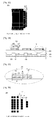
- Fig. 1 is a view illustrating a display apparatus.
- a display apparatus 100 includes a display panel 110, a backlight unit 200, a cover 130, a bottom plate 135, a driver 140, and a rear casing 150.
- the display panel 110 displays an image.
- the display panel 110 includes a first substrate 111, a second substrate 112, and a liquid crystal layer between the first and second substrates 111 and 112.
- the first substrate 111 also referred to as "TFT array substrate” includes a plurality of pixels that are formed at intersections of a plurality of scan lines and a plurality of data lines.
- Thin film transistors (TFTs) are arranged at the respective pixels and connected at respective pixel electrodes.
- the second substrate 112 is also referred to as "color filter substrate".
- the second substrate 112 includes red (R), green (G), and blue (B) color filters respectively corresponding to the plurality of pixels, black matrixes surrounding the respective color filters and covering non-display elements, such as the scan and data lines and TFTs, and a transparent common electrode covering the color filters and the black matrixes.
- a printed circuit board is connected to at least a side of the display panel 110 via a connecting member, such as a flexible circuit board or a tape carrier package (TCP).
- the printed circuit board is brought in tight contact with a rear surface of the bottom plate 135 during modularization.
- the TFTs turn on/off in response to ON/ OFF signals from a gate driver 113 via the scan lines.
- a gate driver 113 When TFTs turn on, data voltages are applied from a data driver 114 to corresponding pixel electrodes via corresponding data lines, so that electric fields are generated between the corresponding pixel electrodes and the common electrode that change arrangement directions of liquid crystal molecules and as a result, causing a change in light transmittance.
- the backlight unit 200 is arranged at a rear surface of the display panel 110 to provide light to the display panel 110.
- the backlight unit 200 includes an optical assembly 123 and a plurality of optical sheets 125 on the optical assembly 123.
- the backlight unit 200 will be described below in detail.
- the display panel 110 and the backlight unit 200 may be modularized with the cover 130 and the bottom plate 135.
- the cover 130 is positioned at a front surface of the display panel 110.
- the cover 130 may be a top cover that is shaped as a rectangular frame to cover top and side surfaces of the display panel 110.
- the cover 130 is open at its front surface so that an image may be viewed from the display panel 110 to outside.
- the bottom plate 135 is positioned at a rear surface of the backlight unit 200.
- the bottom plate 135 may be a bottom cover that is shaped as a rectangular plate.
- the driver 140 is positioned at a surface of the bottom plate 135.
- the driver 140 includes a driving controller 141, a main board 142, and a power supply 143.
- the driving controller 141 is a timing controller that adjusts operating timing of each driving circuit of the display panel 110.
- the main board 142 transmits V-sync and H-sync signals and R, G, and B resolution signals to the driving controller 141.
- the power supply 143 supplies power to the display panel 110 and the backlight unit 200.
- the driver 140 is mounted on a driver chassis 145 and covered by the rear casing 150.
- a backlight unit will now be described in more detail.
- Figs. 2 to 5 are views illustrating a backlight unit.
- a backlight unit 200 includes a first layer 210, a plurality of light sources 220, a second layer 230, and a reflection layer 240.
- the plurality of light sources 220 are formed on the first layer 210.
- the second layer 230 is arranged on the first layer 210 to cover the plurality of light sources 220.
- the first layer 210 is a substrate on which the plurality of light sources 220 and electrode patterns (not shown) for connection to an adaptor (not shown) for supplying power are formed.
- the plurality of light sources 220 and electrode patterns (not shown) for connection to an adaptor (not shown) for supplying power are formed.
- CNT carbon nano tube
- electrode patterns may be formed on the substrate to connect the light sources 220 to the adaptor (not shown).
- the first layer 210 is formed of polyethylene terephthalate (PET), glass, polycarbonate (PC), or silicon (Si).
- the first layer 210 may be a printed circuit board (PCB) or may be formed like a camera film.
- Each light source 220 may be an LED chip or an LED package having an LED chip. An example will be described where the light sources 220 are LED packages.
- LED packages are classified into top view types and side view types depending on the direction in which light emission surfaces are oriented. Top view type LED packages have their light emission surfaces at upper surfaces and side view type LED packages have their light emission surfaces at side surfaces.
- the light sources 220 may employ at least a type of packages of top view type and side view type LED packages.
- the light sources 220 are side view type LED packages
- the light sources 220 have their light emission surfaces at side surfaces and thus emit light in a direction of extension of the first layer 210 or the reflection layer 240.
- the thickness of the second layer 230 may be decreased, resultantly making it possible to render the backlight unit 200 and the display apparatus thinner.
- Each light source 220 may be a colored LED that emits at least one of red, blue, and green light, or a white LED.
- the colored LED may include at least one of a red LED, a blue LED, and a green LED.
- the LEDs may be implemented to have various arrangements and amounts of light.
- the second layer 230 is arranged on the first layer 210 to cover the plurality of light sources 220.
- the second layer 230 transmits and spreads light beams from the light sources 220 so that the light beams may be uniformly provided to the display panel 110.
- the reflection layer 240 is arranged on the first layer 210 to reflect light from the light sources 220.
- the reflection layer 240 includes first and second regions.
- the second region corresponds to a region of the first layer 210 on which the light sources 220 are arranged. Light reflection occurs at the first region.
- the reflection layer 240 does not only reflect light from the light sources but also reflects back light totally reflected by the second layer 230 so that light may be spread over a broader range.
- the reflection layer 240 may include at least one of metals or metal oxides having high reflectivity, such as, for example, aluminum (Al), silver (Ag), gold (Ag), or TiO2.
- the reflection layer 240 may be formed by depositing or coating a metal or a metal oxide on the first layer 210, or by printing a metal ink on the first layer 210.
- the deposition may include vacuum evaporation, such as thermal evaporation or sputtering, and the coating or printing may include a printing method, a gravure coating method, or a silkscreen method.
- the second layer 230 may be formed of a light-transmissive material, such as, for example, a silicon-based or acrylic-based material.
- a light-transmissive material such as, for example, a silicon-based or acrylic-based material.
- the backlight units of this document may not be limited thereto and various resins may be used to form the second layer 230.
- the second layer 230 may be formed of a resin having a refractive index of about 1.4 to about 1.6 so that light from the light sources 220 may be diffused and the backlight unit 200 may have a uniform brightness.
- the second layer 230 may be formed of any one selected from the group consisting of polyethylene terephthalate (PET), polycarbonate (PC), polypropylene (PP), polyethylene (PE), polystyrene (PS), polyepoxy (PE), silicon, and acrylic.
- the second layer 230 may include an adhesive polymer resin allowing the second layer 230 to be firmly attached to the light sources 220 and the reflection layer 240.
- the second layer 230 may be formed of an aciylic-based, urethane-based, epoxy-based, or melamine-based resin, such as, a polymer, a co-polymer, or a terpolymer of, for example, unsaturated polyester, methyl methacrylate, ethylmethacrylate, isobutyl methacrylate, normal butyl methacrylate, normal butyl methyl methacrylate, acrylic acid, methacrylic acid, hydroxyethyl methacrylate, hydroxypropyl methacrylate, hydroxyethyl acrylate, acrylamide, methylolacrylamide, glycidyl methacrylate, ethyl acrylate, isobutyl acrylate, normal butyl acrylate, and 2-ethyl hexy
- the second layer 230 may be formed by applying a liquid or gel resin on the first layer 210 and by curing the resin, or may be formed by applying a resin on a support sheet and by partially curing the resin so that the resin-applied support sheet is attached to the first layer 210.
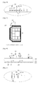
- Fig. 4 is a cross section illustrating a region where no light sources 220 are positioned in the backlight unit 200.
- a region where no light sources 220 are arranged in the backlight unit 200 includes a structure in which the reflection layer 240 covers a top surface of the first layer 210.
- the reflection layer 240 is formed on the first layer 210.
- the reflection layer 240 includes first and second regions.
- the second region corresponds to a region of the first layer 210 on which the light sources 220 are arranged.
- the second region includes holes into which the light sources 220 may be inserted.
- the light sources 220 are projected upwards through the respective holes and are covered by the second layer 230.
- the plurality of light sources 220 have their light emission surfaces at their side surfaces so that light may be radiated in a direction of the side surfaces, for example, in a direction of extension of the first layer 210 or the reflection layer 240.
- the plurality of light sources 220 may be implemented of side view type LED packages. This may reduce a phenomenon that the light sources 220 are viewed as hot spots on the screen as well as may contribute to a decrease in thickness of the second layer 230, thus leading to the backlight unit 200 and resultantly the display apparatus being thinner.
- Light emitted from the light sources 220 may have a predetermined orientation angle ( ⁇ ), for example, 90°C to 150°C, with respect to a first direction (x).
- ⁇ orientation angle
- a direction of light emitted from the light sources 220 is the first direction (x).
- a pattern may be formed on a top surface of the second layer 230 so that light emitted from the light sources 220 through the top surface of the second layer 230 may be reflected and spread. Accordingly, light having a uniform brightness may be emanated from the backlight unit 200.
- Figs. 6 to 9 are views illustrating a backlight unit.
- a third layer 256 is formed on the second layer 230.
- the third layer 256 includes a plurality of light shielding patterns 250 positioned to correspond to the respective light sources 220 and a light transmitting region 254 surrounding the light shielding patterns 250.
- light emitted from the light sources 220 passes through the light transmitting region 254.
- No light shielding patterns 250 are present at the light transmitting region 254.
- the plurality of light shielding patterns 250 are arranged on the second layer 230 to correspond to the respective light sources 220.
- Each light shielding pattern 250 includes a first light shielding film 251 and a reflection film 252.
- the first light shielding film 251 contacts the second layer 230, and the reflection film 252 is formed on top of the first light shielding film 251.
- the first light shielding film 251 shields at least part of light emitted from the light sources 220.
- the reflection film 252 reflects at least part of light emitted from the light sources 220.
- the light shielding patterns 250 may reduce brightness of light coming from regions adjacent to the light sources 220, thus allowing the backlight unit 200 to provide light having a uniform brightness.
- the light shielding patterns 250 selectively shield or reflect light oriented upwards from the light sources 220 to reduce the brightness of light coming from the regions adjacent to the light sources 220 so that the reflected light may spread toward a side surface or a lower surface.
- the first light shielding film 251 includes a metal oxide which is a light shielding material.
- the first light shielding film 251 may include any one or more selected from the group consisting of TiO2, ZnO, and CaCO3.
- the first light shielding film 251 may be formed by depositing or coating the metal oxide or by printing a metal oxide ink according to a pre-determined pattern.
- the metal oxide ink may be a white or whitish ink.
- the first light shielding film 251 may be formed to have a color having a high brightness, for example, white.
- the reflection film 252 includes a light reflecting material, which is a metal.
- the reflection film 252 may include any one or more selected from the group consisting of aluminum (Al), silver (Ag), gold (Au), platinum (Pt), and magnesium (Mg).
- the reflection film 252 may be formed by depositing or coating the metal or by printing a metal ink according to a predetermined pattern.
- the reflection film 252 may have a thickness that stops at least part of light from being transmitted to enhance reflection effects.
- the thickness of the reflection film 252 may be adjusted to provide a proper brightness of light.
- the light shielding patterns 250 shield or reflect light from the light sources 220, thus allowing the backlight unit to provide light of uniform brightness.
- the first light shielding film 251 and the reflection film 252 may be the same in size.
- size may mean an area of a surface of the first light shielding film 251 and the reflection film 252.
- the first light shielding film 251 and the reflection film 252 may be stacked one over another with the same area.
- the order of the first light shielding film 251 and the reflection film 252 is reversed. Specifically, the reflection film 252 is formed on the second layer 230, and the first light shielding film 251 is formed on the reflection film 252. As a result, light emitted from the light source 220 is reflected by the reflection film 252, and light passing through the reflection film 252 is reflected or shielded by the first light shielding film 251.
- the light shielding patterns 250 may be positioned so that centers of the light shielding patterns 250 may be consistent with centers of the respective light sources 220.
- the light shielding patterns 250 may be formed to cover the entire surface of the respective light sources located under the light shielding patterns 250.
- Light emitted from a light source 220 has a maximum brightness at its light emission surface 221. Accordingly, if a light shielding pattern 250 is located over the light emission surface 221 of the light source 220, brightness of light may be reduced at the light emission surface 221 of the light source 220. Since each light source 220 emanates light toward its adjacent light source 220, light reaching a rear surface 222 of a light source 220 is reflected by the light source 220 or the reflection layer 240 adjacent to the light source 220, thus preventing light brightness from increasing at the rear surface 222 of the light source 220.
- the light shielding pattern 250 may be positioned to cover the light emission surface 221 and the rear surface 222 of its corresponding light source 220.
- the light shielding pattern 250 may be located to be biased toward a direction in which light is emitted from the light source 220 to reduce brightness of light at the light emission surface 221 of the light source 220.
- the light shielding patterns 250 are positioned so that centers of the light shielding patterns 250 comply with extension lines L of the respective light sources 220.
- the light shielding patterns 250 in Fig. 8 may be located to be further biased toward the light emission surfaces 221 of the respective light sources 220 than the light shielding patterns 250 in Fig. 7 .
- the light shielding patterns 250 are positioned so that ends of the light shielding patterns 250 comply with extension lines L of the light emission surfaces 221 of the respective light sources 220.
- the light shielding patterns 250 in Fig. 9 may be located to be further biased in the direction of light emission than the light shielding patterns 250 in Fig. 8 .
- the light transmitting region 254 and the light shielding patterns 250 are formed on the second layer 230, light brightness may be reduced at regions adjacent to the light emission surfaces 221 of the light sources 220, thus enhancing uniformity of brightness of the backlight unit.
- Figs. 10 to 13 are views illustrating a backlight unit.
- a backlight unit includes a first layer 210 on which a plurality of light sources 220 are arranged, a reflection layer 240 formed on a surface of the first layer 210 and surrounding the plurality of light sources 220, a second layer 230 covering the reflection layer 240 and the light sources 220, and a third layer 256 formed on the second layer 230.
- the third layer 256 includes a plurality of light shielding patterns 250 positioned to correspond to the respective light sources 220 and light transmitting region 254 surrounding the light shielding patterns 250
- Each light shielding pattern 250 includes a reflection film 252 and a first light shielding film 251 that are different in area from each other.
- the first light shielding film 251 is formed on the second layer 230, and the reflection film 252 is formed on the first light shielding film 251.
- An area of the reflection film 252 is smaller than an area of the first light shielding film 251.
- the reflection film 252 is positioned at a center off the first light shielding film 251.
- the reflection film 252 is formed over the light emission surface 221 of the light source 220 but not over a portion of the light source which is away from the light emission surface 221.
- the reflection film 252 is formed over a portion of the light source 220 which is adjacent to the light emission surface 221 but is not formed over a portion of the light source 220 which is away from the light emission surface 221. Accordingly, manufacturing costs of the reflection films 252 may be saved and light brightness may be reduced at the light emission surface 221 of the light source 220.
- Light reflected by the rear surface 222 of the light source 220 may be reflected again by the first light shielding film 251, thus decreasing brightness of light at the rear surface 222 of the light source 220.
- the order of the first light shielding film 251 and the reflection film 252 may be reversed as shown in Fig. 11 .
- the reflection film 252 is formed on the second layer 230
- the first light shielding film 251 is formed on the reflection film 252.
- the reflection film 252 is formed to be smaller in area than the first light shielding film 251 so that the first light shielding film 251 covers the reflection film 252 and contacts the second layer 230.
- An area of the reflection film 252 may be less than 50% of an area of the first light shielding film 251.
- the area of the reflection film 252 may be 10% to 50% of the area of the first light shielding film 251.
- the area of the reflection film 252 is more than 10% of the area of the first light shielding film 251, brightness of light may be reduced at the light emission surface 221 of the light source 220, and if the area of the reflection film 252 is less than 10% of the area of the first light shielding film 251, manufacturing costs of the reflection film 252 may be reduced and in a case where the reflection film 252 is formed of an ink, a time for drying the ink may be saved.
- the third layer 256 may further include a transparent film 270 as shown in Fig. 12 .
- the light shielding pattern 250 may be formed on the transparent film 270 before being attached on the second layer 230.
- reflection films 252 are formed on a transparent film 270 by deposition, printing, or coating, and then first light shielding films 251 are formed to cover the respective reflection films 252.
- the first light shielding film 251 may be formed of a white ink containing a metal oxide, and the reflection film 252 may be formed of an ink containing a metal.
- the light shielding patterns 250 are attached on the second layer 230 while the light sources 220 are aligned with the respective light shielding patterns 250 as shown in (b) of Fig. 12 , thus completing a backlight unit as shown in (c) of Fig. 12 .
- the transparent film 270 may be directly attached to the second layer 230, thus completing a backlight unit in which the second layer 230, the transparent film 270, and the light shielding patterns 250 are sequentially arranged as shown in Fig. 54 .
- the first light shielding films 251 are provided on the second layer 230, and the reflection films 252 are formed on the respective first light shielding films 251 to cover the respective first light shielding films 251.
- the transparent film 270 may remain, as is, or may be removed later.
- edges of each first light shielding film 251 do not contact the second layer 230
- the edges may be alternately brought in contact with the second layer 230, for example, depending on how much pressure is exerted to the transparent film 270.
- a backlight unit may be formed that is different from the backlight unit shown in Fig. 12 .
- first light shielding films 251 are formed on a transparent film 270 using deposition, printing, or coating, and reflection films 252 are formed on the respective first light shielding films 251 so that the reflection films 252 are aligned with centers of the respective first light shielding films 251.
- the reflection films 252 are formed on the second layer 230, and the first light shielding films 251 are formed on the respective reflection films 252.
- the transparent film 270 may remain, as is, or may be removed later.
- edges of each first light shield film 251 does not contact the second layer 230
- the edges may be alternately brought in contact with the second layer 230, for example, depending on how much pressure is exerted to the transparent film 270.
- Each light shielding pattern 250 may sequentially include a first light shielding film, a reflection film, and a second light shielding film.
- Figs. 14 to 18 are views illustrating a backlight unit.
- the same reference numerals may be used to denote the same or substantially the same elements as those described in connection with Figs. 6 to 13 .
- a third layer 256 is formed on the second layer 230.
- the third layer 256 includes a plurality of light shielding patterns 250 positioned to correspond to the respective light sources 220 and light transmitting region 254 surrounding the plurality of light shielding patterns 250.
- the plurality of light shielding patterns 250 are formed on the second layer 230 to correspond to the respective light sources 220.
- Each light shielding pattern 250 includes a first light shielding film 251, a reflection film 252 on the first light shielding film 251, and a second light shielding film 253 on the reflection film 252.
- the first light shielding film 251 is formed to contact the second layer 230.
- the first light shielding film 251 and the second light shielding film 253 shield at least a part of light emitted from the light source 220, and the reflection film 252 reflects at least a part of light emitted from the light source 220.
- the light shielding patterns 250 are formed on the second layer 230 to reduce brightness of light emitted from regions adjacent to the light sources 220, so that light of uniform brightness may be emitted from the backlight unit 200.
- the light shielding patterns 250 positioned at the respective corresponding light sources 220 on the second layer 230 selectively shield or reflect light emitted upwards from the light sources 220 so that brightness of light coming from regions adjacent to the light sources 220 may be reduced and the reflected light may be diffused toward a side surface or a lower surface.
- the second light shielding film 253 includes a light shielding material, which is a metal oxide, like the first light shielding film 251.
- the metal oxide may include any one or more selected from the group consisting of TiO2, ZnO, and CaCO3.
- the second light shielding film 253 may be formed by deposition or coating of the metal oxide or by printing, e.g., a metal oxide ink according to a predetermined pattern.
- the metal oxide ink may be a white or whitish ink.
- the first and second light shielding films 251 and 253 may be formed to have a color having a high brightness, for example, white.
- the light shielding patterns 250 may shield or reflect light emitted from the light sources 220 to allow the backlight unit to provide a uniform light brightness.
- Fig. 15 is a view illustrating paths of light beams emitted from light sources.
- a light beam 2 from the first light source 220 is reflected by the reflection layer 240 and then by a first light shielding film 251 of a second light shielding pattern 250 arranged over the second light source 220, and then enters into the second layer 230.
- a light beam 3 from the first light source 220 reaches a reflection film 252 of the second light shielding pattern 250 via 230, and is then reflected by the reflection film 252 to travel in the light transmitting region 254.
- a light beam 4 from the first light source 220 is reflected toward the reflection layer 240 by a first light shielding film 251 of a first light shielding pattern 250 arranged over the first light source 220, reflected again by the reflection layer 240, and then travels in the light transmitting region 254.
- a light beam 5 from the first light source 220 passes through the first light shielding film 251 of the first light shielding pattern 250, is reflected by the reflection film 252, and then travels in the light transmitting region 254.
- the light shielding pattern 250 may reflect entirety of light coming through the first light shielding film 251 and the second light shielding film 253 or may partially reflect and partially transmit light coming through the first light shielding film 251 and the second light shielding film 253.
- the reflection film 252 may reflect a part of incident light.
- Such features of the light shielding pattern 250 may be adjusted by controlling light transmittance through the second layer 230.
- light emitted from the light source 220 may spread over a broad range toward a side direction as well as toward other directions without being concentrated on a upper direction, thus allowing the backlight unit 200 to provide light of uniform brightness.
- the light shielding pattern 250 may include the first light shielding film 251, the reflection film 252, and the second light shielding film 253 that are of the same size.
- size here may refer to an area of the first light shielding film 251, the reflection film 252, and the second light shielding film 253.
- the first light shielding film 251, the reflection film 252, and the second light shielding film 253 may have the same area.
- the light shielding patterns 250 may be positioned so that their centers comply with centers of the respective light sources 220.
- the light shielding patterns 250 may be positioned to fully cover the respective corresponding light sources 220.
- Light emitted from a light source 220 has the maximum brightness at a light emission surface 221 of the light source 220. Accordingly, brightness of light at the light emission surface 221 of the light source 220 may be reduced by locating a light shielding pattern 250 over the light emission surface 221.
- a light source 220 directs light toward a neighboring light source 220. Light reaching a rear surface 222 of the neighboring light source 220 is reflected by the neighboring light source 220 or by the reflection layer 240 adjacent to the neighboring light source 220, thus preventing light brightness from increasing at the rear surface 222.
- the light shielding pattern 250 may be positioned over both the light emission surface 221 and the rear surface 222 of the light source 220.
- the light shielding pattern 250 may be located to be biased in a direction of emission of light from the light source 220 to reduce brightness of light at the light emission surface 221 of the light source 220.
- light shielding patterns 250 are positioned so that centers of the light shielding patterns 250 comply with extension lines L of light emission surfaces 221 of respective light sources 220.
- the light shielding patterns 250 shown in Fig. 16 are arranged to be further biased in the direction of light emission than the light shielding patterns 250 in Fig. 14 .
- the light shielding patterns 250 are positioned so that their centers are biased further in a direction of light emission of the light sources 220 than extension lines L of the light emission surfaces 221 of the respective light sources 220.
- the light shielding patterns 250 shown in Fig. 17 are arranged to be further biased in the direction of light emission than the light shielding patterns 250 in Fig. 16 .
- the light shielding patterns 250 are positioned so that ends of the light shielding patterns 250 comply with extension lines L of the light emission surfaces 221 of the respective light sources 220.
- the light shielding patterns 250 in Fig. 18 may be located to be further biased in the direction of light emission than the light shielding patterns 250 in Fig. 17 .
- the light shielding patterns 250 may reduce light brightness at regions adjacent to the light emission surfaces 221 of the light sources 220, thus allowing the backlight unit to provide uniform brightness.
- Figs. 19 to 21 are views illustrating a backlight unit.
- a backlight unit includes a first layer 210, a plurality of light sources 220, a reflection layer 240 formed on the first layer 210 to surround the plurality of light sources 220, a second layer 230 formed on the reflection layer 240 and the light sources 220, and a third layer 256 formed on the second layer 230.
- the third layer 256 includes a plurality of light shielding patterns 250 positioned to correspond to the respective light sources 220 and light transmitting region 254 surrounding the light shielding patterns 250.
- each light shielding pattern 250 includes a first light shielding film 251, a reflection film 252 formed on the first light shielding film 251, and a second light shielding film 252 formed on the reflection film 252.
- the reflection film 252 has a different area from an area of the first light shielding film 251 and the reflection film 252.
- the light shielding patterns 250 are positioned to correspond to the respective light sources 220.
- the first light shielding film 251 is formed to contact the second layer 230.
- the reflection film 252 has a smaller area than an area of 251.
- the second light shielding film 253 covers the reflection film 252 and contacts part of the first light shielding film 251.
- the reflection film 252 is formed over the light emission surface 221 of the light source 220 but not over a portion of the light source which is away from the light emission surface 221.
- the reflection film 252 is formed over a portion of the light source 220 which is adjacent to the light emission surface 221 but is not formed over a portion of the light source 220 which is away from the light emission surface 221. Accordingly, manufacturing costs of the reflection films 252 may be saved and light brightness may be reduced at the light emission surface 221 of the light source 220.
- Light reflected by the rear surface 222 of the light source 220 may be reflected again by the first light shielding film 251 and the second light shielding film 253, thus decreasing brightness of light at the rear surface 222 of the light source 220.
- the reflection films 252 are formed over the light emission surfaces 221, and the first and second light shielding films 251 and 253 are biased further in the direction of light emission than the reflection films 252.
- the reflection film 252 is formed to be adjacent to the light emission surface 221 of the light source 220, for example, over the light emission surface 221, and the first light shielding film 251 and the second light shielding film 253 are formed to be away from the light emission surface 221 of the light source 220 to reduce brightness of light at the light emission surface 221 of the light source 220.
- An area of the reflection film 252 may be less than 50% of an area of the first light shielding film 251 or the second light shielding film 253.
- the area of the reflection film 252 may be 10% to 50% of the area of the first light shielding film 251 or the second light shielding film 253.
- the area of the reflection film 252 is more than 10% of the area of the first light shielding film 251 or the second light shielding film 253, brightness of light may be reduced at the light emission surface 221 of the light source 220, and if the area of the reflection film 252 is less than 10% of the area of the first light shielding film 251 or the second light shielding film 253, manufacturing costs of the reflection film 252 may be reduced and in a case where the reflection film 252 is formed of an ink, a time for drying the ink may be saved.
- each reflection film 252 includes two patterns. Each reflection film 252 may include two or more patterns.
- the reflection film 252 includes two patterns on the first light shielding film 251, which are positioned to correspond to the light emission surface 221 and 222, respectively.
- no reflection film 252 is formed over a center of the light source 220 since light brightness is not high at the center of the light source 220 while the two patterns of the reflection film 252 are arranged over the light emission surface 221 and the rear surface 222 which have high light brightness.
- light brightness may be reduced at the light emission surface 221 and the rear surface 222 of the light source 220 while saving manufacturing costs of the reflection film 252.
- the first light shielding film 251, the reflection film 252, and the second light shielding film 253 may have different sizes.
- Figs. 22 to 25 are views illustrating a backlight unit.
- a backlight unit includes a first light shielding film 251, a reflection film 252, and a second light shielding film 253 that have different sizes from each other.
- the light shielding patterns 250 are formed to correspond the respective light sources 220.
- the first light shielding film 251 is formed to contact the second layer 230, the reflection film 252 is formed on the first light shielding film 251 to correspond to the light emission surface 221 of the light source 220, and the second light shielding film 253 is formed on the reflection film 252.
- a size of the first light shielding film 251 is larger than a size of the reflection film 252 a size of which is larger than a size of the second light shielding film 253.
- the first light shielding film 251 has a largest size
- the second light shielding film 253 has a smallest size.
- the first light shielding film 251, the reflection film 252, and the second light shielding film 253 are all positioned over the light emission surface 221 of the light source 220 so that light brightness may be reduced at the light emission surface 221 of the light source 220.
- the first light shielding film material 25 land the reflection film 252 are positioned over a region of the light source 220 which is from a center of the light source 220 to the rear surface 222, so that light brightness may be reduced at the region.
- the size of the first light shielding film 251, the reflection film 252, and the second light shielding film 253 gradually decreases in the order of the first light shielding film 251, the reflection film 252, and the second light shielding film 253 in the direction of light emission from the light emission surface 221.
- the first light shielding film 251, the reflection film 252, and the second light shielding film 253 are all positioned over the light emission surface 221, but only the first light shielding film 251 is positioned over a region of the light source 220 which is away from the light emission surface 221 in the direction of light emission.
- the first light shielding film 251, the reflection film 252, and the second light shielding film 253 are sequentially stacked in the form of a pyramid.
- the first light shielding film 251 contacting the second layer 230 has a largest size.
- the reflection film 252 formed on the first light shielding film 251 has a size smaller than a size of the first light shielding film 251 and is arranged so that its center complies with a center of the first light shielding film 251.
- the second light shielding film 253 formed on the reflection film 252 has a size smaller than a size of the reflection film 252 and is arranged so that its center complies with a center of the reflection film 252.
- the light shielding pattern 250 is formed in the shape of a pyramid so that the light emission surface 221 and the centers of the first light shielding film 251, the reflection film 252, and the second light shielding film 253 are aligned with one another.
- the first light shielding film 251, the reflection film 252, and the second light shielding film 253 are all positioned over the light emission surface 221 of the light source 220 so that light brightness may be reduced at the light emission surface 221 of the light source 220.
- the light shielding patterns 250 may be formed on the second layer 230 as described in connection with Figs. 12 and 13 .
- the second light shielding film 253 is formed on a transparent film 270 by deposition, printing, or coating.
- the reflection film 252 is formed on the second light shielding film 253 to have a smaller size than a size of the second light shielding film 253, and the first light shielding film 251 is formed on the reflection film 252 to cover the reflection film 252.
- the light shielding patterns 250 are attached on the second layer 230 while the light sources 220 are aligned with the respective light shielding patterns 250 as shown in (b) of Fig. 25 , thus completing a backlight unit as shown in (c) of Fig. 25 .
- the transparent film 270 may be directly attached to the second layer 230, thus completing a backlight unit in which the second layer 230, the transparent film 270, and the light shielding patterns 250 are sequentially arranged as shown in Fig. 54 .
- the first light shielding films 251 are provided on the second layer 230, and the reflection films 252 are formed on the respective first light shielding films 251 to cover the respective first light shielding films 251.
- the second light shielding films 253 are respectively formed on the reflection films 252 and the first light shielding films 251.
- the transparent film 270 may remain, as is, or may be removed later.
- edges of each first light shielding film 251 do not contact the second layer 230
- the edges may be alternately brought in contact with the second layer 230, for example, depending on how much pressure is exerted to the transparent film 270.
- Figs. 26 to 28 are plan views illustrating a light transmitting region and light shielding patterns included in a backlight unit.
- the light shielding pattern 250 has a circular or elliptical shape with respect to its corresponding light source 220.
- a center of the light shielding pattern 250 complies with a center of the light source 220.
- the light shielding pattern 250 may have the same or different shapes or sizes.
- the light shielding pattern 250 is slightly shifted in the direction of light emission, for example, in the x-axial direction, so that its center is biased by a predetermined distance in the direction of light emission with respect to a center of the corresponding light source 220.
- the light shielding pattern 250 is further shifted in the direction of light emission than the light shielding pattern 250 shown in Fig. 27 , so that only a part of the light source 220 overlaps the light shielding pattern 250.
- Fig. 29 is a view illustrating a few light shielding patterns having different shapes.
- the light shielding pattern 250 may have a circular shape as shown in (a) of Fig. 29 and an elliptical shape as shown in (b) of Fig. 29 with respect to the corresponding light source 220. Reflection features of the light shielding pattern 250 may be adjusted depending on the location of the first light shielding film, the second light shielding film, and the reflection film as the light shielding pattern 250 goes from a center to an outside. For example, reflectivity of the light shielding pattern 250 may gradually decrease in the direction from the center of the light shielding pattern 250 to the outside.
- the light transmittance or aspect ratio of the light shielding pattern 250 may increase in the direction from the center to the outside. Accordingly, the light shielding pattern 250 may have the maximum reflectivity (for example, most of light does not pass through a corresponding region) and the minimum light transmittance and aspect ratio at a region where the corresponding light source 220 is formed, specifically, at the center of the light shielding pattern 250, which corresponds to a center of the light source 220. Resultantly, it may be possible to more effectively prevent a hot spot from occurring at the region where the light source 220 is formed due to concentration of light.
- a center of the light shielding pattern 250 which overlaps the light source 220 may have an aspect ratio less than 5% to prevent the hot spot.
- the light shielding pattern 250 is shaped to have a plurality of elongated protrusions protruding in the direction of light emission. Light may be shielded or reflected at a region where light is emitted by the light shielding pattern 250, and light may be partially transmitted or partially reflected along the direction of light emission by the plurality of protrusions, thus preventing a hot spot from occurring at a region adjacent to the light source.
- Figs. 30 to 32 illustrate a backlight unit and light shielding patterns according to embodiments of this document.
- Fig. 30 is a plan view illustrating light shielding patterns according to an embodiment of this document.
- Fig. 31 is a view illustrating a backlight unit having light shielding patterns according to an embodiment of this document.
- Fig. 32 is an expanded view illustrating region P1 of Fig. 31 .
- a third layer 256 includes a plurality of light shielding patterns 250 and a light transmitting region 254 surrounding the plurality of light shielding patterns 250.
- the light transmitting region 254 includes a first region A1 adjacent to the light source 220 and a second region A2 away from the light source 220.
- the first region A1 is smaller in area than the second region A2.
- the light transmitting region 254 includes regions between the plurality of light shielding patterns 250.
- a backlight unit includes a first layer 210, a plurality of light sources 220 on the first layer 210, a reflection layer 240 on the first layer 210 to surround the plurality of light sources 220, a second layer 230 covering the reflection layer 240 and the light sources 220, and the light transmitting region 254 and the plurality of light shielding patterns 250 on the second layer 230.
- the first region A1 is smaller in area than the second region A2. According to an embodiment, as a distance from the light source 220 increases, an area occupied by the light transmitting region 254 may increase or may first increase and may be then maintained as is since a predetermined distance.
- Each light shielding pattern 250 includes a first light shielding film 251, a reflection film 252, and a second light shielding film 253 that are sequentially stacked.
- widths of the light shielding patterns 250 decrease and intervals between the light shielding patterns 250 increase. For example, as a distance from the light source 220 increases in the direction of light emission, more and more portions of the light transmitting region 254 show up.
- a light shielding pattern 250 closest to the light emission surface 221 of the light source 220 has a largest width W1.
- the widths W1 of the light shielding patterns 250 decrease in the direction of light emission.
- intervals W2 between two neighboring light shielding patterns 250 increase as the light shielding patterns 250 are away from the light source 220, for example, in the direction of light emission.
- an area occupied by the light transmitting region 254 increases in the direction of light emission while light brightness may be reduced at the light emission surface 221 of the light source 220, brightness of light may be made uniform at the regions adjacent to and away from the light source 220, thus allowing the backlight unit to provide uniform light brightness.
- Figs. 33 to 35 illustrate a backlight unit and light shielding patterns according to embodiments of this document.
- Fig. 33 is a plan view illustrating light shielding patterns according to an embodiment of this document.
- Fig. 34 is a view illustrating a backlight unit having light shielding patterns according to an embodiment of this document.
- Fig. 35 is an expanded view illustrating region P2 of Fig. 34 .
- the light transmitting region 254 includes a first region A1 adjacent to the light source 220 and a second region A2 away from the light source 220.
- the first region A1 is smaller in area than the second region A2. According to an embodiment, as a distance from the light source 220 increases, an area occupied by the light transmitting region 254 may increase or may first increase and may be then maintained as is since a predetermined distance.
- Widths W1 of the light shielding patterns 250 decrease as the light shielding patterns 250 are away from the light source 220, and intervals between two neighboring light shielding patterns 250 remain constant. For example, as the widths W1 of the light shielding patterns 250 decrease, more and more portions of the light transmitting region 254 appear.
- a light shielding pattern 250 closest to the light emission surface 221 of the light source 220 has a largest width W1.
- the widths W1 of the light shielding patterns 250 gradually decrease as the light shielding patterns 250 are away from the light source 220.
- Intervals W2 of two neighboring light shielding patterns 250 remain constant.
- light brightness may be reduced at the light emission surface 221 of the light source 220, and an area occupied by the light transmitting region 254 increases in the direction away from the light source 220.
- aperture ratios increase as the widths of the light shielding patterns 250 decrease although the light shielding patterns 250 have the same interval.
- light brightness is made uniform at regions adjacent to the light source 220 and away from the light source 220, thus allowing the backlight unit to provide light of uniform brightness.
- Figs. 36 to 38 illustrate a backlight unit and light shielding patterns according to embodiments of this document.
- Fig. 36 is a plan view illustrating light shielding patterns according to an embodiment of this document.
- Fig. 37 is a view illustrating a backlight unit having light shielding patterns according to an embodiment of this document.
- Fig. 38 is an expanded view illustrating region P3 of Fig. 37 .
- the light transmitting region 254 includes a first region A1 adjacent to the light source 220 and a second region A2 away from the light source 220.
- the first region A1 is smaller in area than the second region A2. According to an embodiment, as a distance from the light source 220 increases, an area occupied by the light transmitting region 254 may increase or may first increase and may be then maintained as is since a predetermined distance.
- the light shielding patterns 250 are of the same width W1 and as the light shielding patterns 250 are away from the light source 220, intervals W2 between two neighboring light shielding patterns 250 increase. For example, as the intervals W2 between two neighboring light shielding patterns 250 increase, more and more portions of the light transmitting region 254 appear.
- the plurality of light shielding patterns 250 have the same width W1 and the intervals W2 between two neighboring light shielding patterns 250 increase in the direction away from the light source 220.
- light brightness may be reduced at a region adjacent to the light emission surface 221 of the light source 220 since the interval W2 is narrow. As being away from the light source 220, the intervals W2 increase so that an area occupied by the light transmitting region 254 increases. This makes light brightness uniform at regions adjacent to the light source 220 and away from the light source 220, thus allowing the backlight unit to provide light of uniform brightness.
- Figs. 39 to 41 illustrate various arrangements of light shielding patterns having different shapes.
- a plurality of light shielding patterns 250 have a pentagonal arrangement.
- the plurality of light shielding patterns 250 have the same widths and intervals at a region adjacent to the light shielding pattern 250, and the widths and intervals of the light shielding patterns 250 decrease and increase, respectively, as the light shielding patterns 250 are away from the light source 220.
- the widths and intervals of the light shielding patterns 250 decrease and increase, respectively, as the light shielding patterns 250 are away from the light source 220.
- each light shielding pattern 250 has a circular shape. As the light shielding patterns 250 are away from their center to their outside, the widths remain constant and the intervals increase. However, the embodiments of this document are not limited thereto, and any arrangement or shapes of the light shielding patterns may be adopted as long as more and more portions of the light transmitting region 254 show up as the light shielding patterns are away from the light source 220.
- the light shielding pattern may have a plurality of holes to adjust the area occupied by the light transmitting region 254.
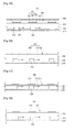
- Figs. 42 to 44 illustrate a backlight unit and a plurality of light shielding patterns according to embodiments of this document.
- Fig. 42 is a plan view illustrating light shielding patterns according to an embodiment of this document.
- Fig. 43 is a view illustrating a backlight unit having light shielding patterns according to an embodiment of this document.
- Fig. 44 is an expanded view illustrating region P4 of Fig. 43 .
- a plurality of light shielding patterns 250 include a plurality of holes 260.
- a backlight unit includes a first layer 210, a plurality of light sources 220 on the first layer 210, a reflection layer 240 on the first layer 210 to surround the plurality of light sources 220, a second layer 230 covering the reflection layer 240 and the light sources 220, and a third layer 256 on the second layer 230.
- the third layer includes a plurality of light shielding patterns 250 positioned to correspond the respective light sources 220 and a light transmitting region 254 surrounding the plurality of light shielding patterns 250.
- the light transmitting region 254 includes a first region A1 adjacent to the light source 220 and a second region A2 away from the light source 220.
- the first region A1 is smaller in area than the second region A2.
- the light transmitting region 254 includes regions between the plurality of light shielding patterns 250. According to an embodiment, as a distance from the light source 220 increases, an area occupied by the light transmitting region 254 may increase or may first increase and may be then maintained as is since a predetermined distance.
- Each light shielding pattern 250 includes a first light shielding film 251, a reflection film 252, and a second light shielding film 253 that are sequentially stacked.
- the light shielding patterns 250 include a plurality of holes 260 through which light is emitted from the light sources 220 to outside. The area occupied by the light transmitting region 254 is adjusted by the number and size of the holes 260.
- widths of the holes 260 increase.
- a hole 260 closest to the light emission surface 221 of the light source 220 has a largest width W3, and as the holes 260 are away from the light source 220, the widths W3 of the holes 260 gradually increase and intervals W4 between two neighboring holes 260 decrease.
- an area occupied by the light transmitting region 254 increases. This makes light bright uniform at regions adjacent to and away from the light source 220, thus allowing the backlight unit to provide light of uniform brightness.
- Figs. 45 to 47 illustrate a backlight unit and a plurality of light shielding patterns according to embodiments of this document.
- Fig. 45 is a plan view illustrating light shielding patterns according to an embodiment of this document.
- Fig. 46 is a view illustrating a backlight unit having light shielding patterns according to an embodiment of this document.
- Fig. 47 is an expanded view illustrating region P5 of Fig. 46 .
- the light transmitting region 254 includes a first region A1 adjacent to the light source 220 and a second region A2 away from the light source 220.
- the first region A1 is smaller in area than the second region A2.
- the light transmitting region 254 includes regions between the plurality of light shielding patterns 250. According to an embodiment, as a distance from the light source 220 increases, an area occupied by the light transmitting region 254 may increase or may first increase and may be then maintained as is since a predetermined distance.
- the light shielding patterns 250 include a plurality of holes 260. Widths W3 of the holes 260 increase and intervals W4 between two neighboring holes 260 remain constant as the holes 260 are away from the light source 220.
- a hole 260 closest to the light emission surface 221 of the light source 220 has a largest width W3.
- the widths W3 of the holes 260 increase while the intervals W4 are left unchanged.
- the width W3 and the interval W4 are small near the light emission surface 221 of the light source 220, light brightness may be reduced at the light emission surface 221.
- the intervals W4 increase and an area occupied by the light transmitting region 254 resultantly increases. This makes light bright uniform at regions adjacent to and away from the light source 220, thus allowing the backlight unit to provide light of uniform brightness.
- Figs. 48 to 50 illustrate a backlight unit and a plurality of light shielding patterns according to embodiments of this document.
- Fig. 48 is a plan view illustrating light shielding patterns according to an embodiment of this document.
- Fig. 49 is a view illustrating a backlight unit having light shielding patterns according to an embodiment of this document.
- Fig. 50 is an expanded view illustrating region P6 of Fig. 49 .
- the light transmitting region 254 includes a first region A1 adjacent to the light source 220 and a second region A2 away from the light source 220.
- the first region A1 is smaller in area than the second region A2.
- the light transmitting region 254 includes regions between the plurality of light shielding patterns 250. According to an embodiment, as a distance from the light source 220 increases, an area occupied by the light transmitting region 254 may increase or may first increase and may be then maintained as is since a predetermined distance.
- the light shielding patterns 250 include a plurality of holes 260. Widths W3 of the holes 260 remain constant and intervals W4 between two neighboring holes 260 decrease as the holes 260 are away from the light source 220.
- interval W4 Since the interval W4 is large near the light emission surface 221 of the light source 220, light brightness may be reduced at the light emission surface 221. As the holes 260 are away from the light source 220, the intervals W4 decrease and an area occupied by the light transmitting region 254 resultantly increases. This makes light bright uniform at regions adjacent to and away from the light source 220, thus allowing the backlight unit to provide light of uniform brightness.
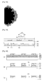
- Figs. 51 and 52 illustrate light shielding patterns having various shapes.
- the light shielding pattern 250 has a circular shape and includes a plurality of holes.
- the plurality of holes constitute a plurality of ring-shaped hole arrays.
- the ring-shaped hole arrays are loosely arranged at a center of the light shielding pattern 250?for example, a less number of holes are positioned and an interval between two neighboring hole arrays is large near the center of the light shielding pattern 250.
- the hole arrays become compact?for example, the number of holes increases and the interval between two neighboring hole arrays decreases. Accordingly, an area occupied by the light transmitting region 254 increases as a distance from the center of the light shielding pattern 250 increases.
- the light shielding pattern 250 has a pentagonal shape whose edges are rounded. As a distance increases from a center of the light shielding pattern 250 to outside, the number of holes increases. Accordingly, an area occupied by the light transmitting region 254 increases as a distance from the center of the light shielding pattern 250 increases.
- the embodiments of this document are not limited thereto, and any arrangement or shapes of the light shielding patterns may be adopted as long as more and more portions of the light transmitting region 254 show up as the light shielding patterns are away from the light source 220.
- the embodiments of this document are not limited thereto.
- the light shielding pattern which has a double layer structure with one or more holes may also be adopted.
- the third layer 256 may be formed by forming the light shielding patterns 250 and the light transmitting region 254 on a transparent film 270, and may be attached on the second layer 230.
- Figs. 53 to 55 are views illustrating a backlight unit and a method of manufacturing the backlight unit in a sequential order.
- a backlight unit includes a first layer 210, a plurality of light sources 220 on the first layer 210, a reflection layer 240 on the first layer 210 to surround the plurality of light sources 220, and a second layer 230 covering the reflection layer 240 and the light sources 220.
- a third layer 256 is formed by forming light shielding patterns 250 and a light transmitting region 254 on a transparent film 270, and is then attached on the second layer 230.
- the transparent film 270 may be formed of a material similar to the second layer 230, such as, for example, an acrylic-based, urethane-based, epoxy-based, or melamine-based resin, such as, a polymer, a co-polymer, or a terpolymer of, for example, unsaturated polyester, methyl methacrylate, ethylmethacrylate, isobutyl methacrylate, normal butyl methacrylate, normal butyl methyl methacrylate, acrylic acid, methacrylic acid, hydroxyethyl methacrylate, hydroxypropyl methacrylate, hydroxyethyl acrylate, acrylamide, methylolacrylamide, glycidyl methacrylate, ethyl acrylate, isobutyl acrylate, normal butyl acrylate, and 2-ethyl hexyl acrylate.
- the backlight units of this document are not limited thereto, and any material having high
- the third layer 256 may be formed by first forming the first light shielding film 251, the reflection film 252, and the second light shielding film 253 on the transparent film 270 and then by attaching the transparent film 270 to the second layer 230 so that the plurality of light sources 220 are aligned with the plurality of respective light shielding patterns 250.
- a first light shielding film material 251a, a reflection film material 252a, and a second light shielding film material 253a are sequentially formed on a transparent film 270.
- the first light shielding film material 251a and the second light shielding film material 253a may be printed with a white ink containing a metal oxide, and the reflection film material 252a may be printed with an ink containing a metal.
- a mask layer 275 is formed on the second light shielding film material 253a.
- the mask layer 275 may be formed of a material unreactive with the first light shielding film material 251a, the reflection film material 252a, and the second light shielding film material 253a.
- the mask layer 275 may be formed of an ink including organic and inorganic particles.
- first light shielding films 251, reflection films 252, and second light shielding films 253 are formed.
- the remaining mask layer 275 is then removed, thus forming light shielding patterns 250 that includes the first and second light shielding films 251 and 253 on the transparent film 270.
- the backlight units of this document are not limited thereto.
- the light shielding patterns may also be manufactured using a laser transfer process or physical etching process.
- a diffusing plate 280 is formed on the backlight unit.
- the diffusing plate 280 diffuses light emitted from the backlight unit to an outside, thus allowing the backlight unit to provide further uniform light brightness.
- the diffusing plate 280 may also be spaced apart from the transparent film 270.
- the third layer 256 obtained by forming the light shielding patterns 250 and the light transmitting region 254 on the transparent film 270 is attached to the second layer 230.
- the transparent film 270 is positioned on the second layer 230, and the light shielding patterns 250 and the light transmitting region 254 are positioned on the transparent film 270.
- the light shielding patterns 250 and the light transmitting region 254 are formed on the transparent film 270, and are then attached onto the second layer 230. Such a structure facilitates its manufacturing processes, thus enhancing productivity.
- the backlight units have been described where the transparent film 270 and/or the diffusing plate 280 are formed on the light shielding patterns 250. However, the backlight units of this document are not limited thereto.
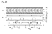
- Fig. 57 is a view illustrating a backlight unit.
- a reflection layer 240 is formed on a first layer 210.
- the reflection layer 240 includes a plurality of holes through which the respective corresponding light sources 220 are inserted.
- the light sources 220 are protruded upwards through the respective holes and are surrounded by a second layer 230.
- a third layer 256 is formed on the light sources 220.
- the third layer 256 includes a transparent film 270, light shielding patterns 250 on the transparent film 270, and a light transmitting region 254.
- the transparent film 270 is brought in tight contact with upper portions of the light sources 220.
- the second layer 230 between the reflection layer 240 and the transparent film 270 may be formed of an air layer.
- the backlight unit is manufactured by attaching the third layer 256 on the light sources 220. Therefore, the backlight unit may be easily manufactured with enhanced productivity.
- the light shielding patterns 250 are formed of a single layer, the backlight units of this document are not limited thereto.
- the light shielding patterns 250 may be formed of a dual layer or a triple layer.
- Fig. 58 is a view illustrating a backlight unit.
- the light shielding patterns 250 are formed of a single layer. Specifically, a plurality of light sources 220 are formed on a first layer 210, a reflection layer 240 is formed on the first layer 210 to reflect light emitted from the plurality of light sources 220, and a second layer 230 is formed to cover the plurality of light sources 220 and the reflection layer 240. Further, a third layer 256 is formed on the second layer 230. The third layer 256 includes a plurality of light shielding patterns 250 and a light transmitting region 254 surrounding the plurality of light shielding patterns 250. The plurality of light shielding patterns 250 are positioned to correspond to the respective light sources 220.
- the light shielding patterns 250 are formed of a single layer.
- the single layer may include one of a light shielding film and a reflection film.
- the light shielding patterns 250 may serve as a light shielding film that shields at least a part of light emitted from the light sources 220.
- the light shielding patterns 250 may function as a reflection film that reflects at least a part of light emitted from the light sources 220.
- the light shielding film and the reflection film are the same as the light shielding film and the reflection film described in connection with Figs. 6 to 57 .
- the light shielding patterns 250 By forming the light shielding patterns 250 on the second layer 230, it may be possible to reduce brightness of light coming from regions adjacent to the light sources 220, thus allowing the backlight unit 200 to provide light of uniform brightness.
- the light shielding patterns 250 are formed on the second layer 230 to correspond to the respective light sources 220 and selectively shields or reflects light emitted upwards from the light sources 220, thus reducing brightness of light coming from the regions adjacent to the light sources 220.
- the reflected light may be diffused toward a side surface or a lower side.
- Fig. 59 is a cross sectional view illustrating a display apparatus.
- Fig. 59 is a cross sectional view taken along line U-U' of Fig. 1 .
- the same reference numerals may be used to denote the same or substantially the same elements as those described in connection with Figs. 1 to 59 .
- a display panel 110 includes a first substrate 111, a second substrate 112, an upper polarizing plate 160a, and a lower polarizing plate 160b.
- a backlight unit 200 includes a first layer 210, a plurality of light sources 220, and a second layer 230. The display panel 110 is brought in tight contact with the backlight unit 200.
- An adhesive is applied between the display panel 110 and the backlight unit 200 so that the backlight unit 200 may be attached and fixed to a lower surface of the display panel 110.
- an upper surface of the backlight unit 200 is attached to a lower surface of the lower polarizing plate 160b by an adhesive 170.
- the backlight unit 200 includes a plurality of light sources 220 on the first layer 210, a reflection layer 240 surrounding the plurality of light sources 220, a second layer 230 on the reflection layer 240, and a plurality of light shielding patterns 250 each having a first light shielding film, a reflection film, and a second light shielding film.
- a transparent film 270 is formed on the light shielding patterns 250, and a diffusing plate 280 is formed on the transparent film 270.
- the backlight units of this document are not limited thereto. For example, the backlight units described in connection with Figs. 1 to 55 may be adopted.
- a bottom plate 135 is arranged under the backlight unit 200 so that the bottom plate 135 is brought in tight contact with a lower surface of the first layer 210.
- the backlight unit 200 may include a plurality of blocks that may be driven separately from each other.
- the display apparatus includes a display module, for example, a driver that supplies driving signals and power to the display panel 110 and the backlight unit 200.
- a display module for example, a driver that supplies driving signals and power to the display panel 110 and the backlight unit 200.
- the plurality of light sources 220 in the backlight unit 200 generate light using power supplied from the driver.
- the driver includes a driving controller 141, a main board 142, and a power supply 143.
- the driver is arranged and fastened on a driver chassis 145 that is provided on the bottom plate 135, so that the driver may be stably supported and fixed.
- a first connector 310 is provided on a rear surface of the first layer 210.
- the bottom plate 135 includes a hole 350 through which the first connector 310 is inserted.
- the first connector 310 electrically connects the light sources 220 to the power supply 143 so that driving voltages may be supplied from the power supply 143 to the light sources 220.
- the first connector 310 is formed on a lower surface of the first layer 210 and is connected through a first cable 410 to the power supply 143 so that driving voltages may be supplied from the power supply 143 to the light sources 220 through the first cable 410.
- An electrode pattern (not shown), such as a carbon nano-tube electrode pattern, may be formed on an upper surface of the first layer 210 and may contact electrodes of the light sources 220 to electrically connect the first connector to the light sources 220.
- the driving controller 141 such as, for example, a timing controller, controls driving of the display panel 110 and the backlight unit 200.
- the timing controller controls driving timing of the display panel 110. Specifically, the timing controller supply the display panel 110 with signals for controlling driving timing of a data driver (not shown), a gamma voltage generator (not shown), and a gate driver (not shown) provided in the display panel 110.
- a data driver not shown
- a gamma voltage generator not shown
- a gate driver not shown
- the timing controller may supply the backlight unit 200 with signals for controlling driving timing of the light sources 220 so that the backlight unit 200, more specifically, the light sources 220, are operated in synchronization with the operation of the display panel 110.
- the driving controller 141 is fastened on the driver chassis 145 to be stably supported and fixed by the driver chassis 145.
- a second connector 320 is provided on the first layer 210.
- the bottom plate 135 includes a hole 350 through which the second connector 320 is inserted.
- the second connector 320 electrically connects the first layer 210 to the driving controller 141 so that control signals may be supplied from the driving controller 141 to the first layer 210.
- the second connector 320 is formed on a lower surface of the first layer 210 and is connected through a second cable 420 to the driving controller 141 so that control signals may be supplied from the driving controller 141 to the first layer 210 through the second cable 420.
- a light source driver (not shown) may be provided on the first layer 210 and may drive the light sources 220 using the control signals supplied from the driving controller 141 through the second connector 320.
- the power supply 143 and the driving controller 141 are covered by a rear casing 150 to be protected from the outside.
- the display apparatus illustrated in Fig. 59 is merely an example.
- the arrangement or number of the power supply 143, the driving controller 141, the first and second connectors 310 and 320, and the first and second cables 410 and 420 may vary as necessary.
Landscapes
- Physics & Mathematics (AREA)
- Nonlinear Science (AREA)
- Mathematical Physics (AREA)
- Chemical & Material Sciences (AREA)
- Crystallography & Structural Chemistry (AREA)
- General Physics & Mathematics (AREA)
- Optics & Photonics (AREA)
- Planar Illumination Modules (AREA)
- Devices For Indicating Variable Information By Combining Individual Elements (AREA)
Description
- This document is directed to a backlight unit and a display apparatus including the backlight unit.
- Due to the advantages of compact, lightweight, and low power consumption, liquid crystal display ("LCD") apparatuses have various applications, such as in laptop computers, personal computers, or monitors.
- A LCD apparatus includes a LCD panel and a backlight unit. The backlight unit provides light to the LCD panel. The light transmits the LCD panel. The LCD panel controls transmittance of the light to display an image.
- Backlight units may be classified into edge types and direct types. An edge-type backlight unit includes a light source at a side surface of the LCD panel and a light guide plate at a rear surface of the LCD panel. The light guide plate guides light from the light source to the LCD panel. A direct-type backlight unit includes a plurality of light sources at a rear surface of the LCD. The plurality of light sources directly supply light to the LCD panel.
- EL (electro luminescence) lamps, CCFLs (cold cathode fluorescent lamps), HCFLs (hot cathode fluorescent lamps), LEDs (light emitting diodes) are used as light sources. LEDs have the advantages of low power consumption and high emission efficiency.
- Document
WO2010035566 discloses an illuminating device including a point light source and an optical member disposed closer to the light exit side of the illuminating device than the point light source, the optical member is formed of a member having a generally uniform light transmittance and has a first light reflecting portion for reflecting light from the point light source in the area which is superposed on the point light source when viewed from above, and the illuminating device further includes second light reflecting portions for reflecting light reflected from the first light reflecting portion toward the first light reflecting portion. - However, backlight units have a non-unformity of a luminance due to a hot-spots.
- The above problem is solved by the claimed matter according to the independent claims.
- Backlight units according to the present invention are defined in claims 1 and 2, respectively. A display apparatus according to the present invention is defined in claim 11.
- The backlight unit and display apparatus provide a light shielding patterns to prevent hot spots from occurring at regions adjacent to light sources so that the backlight unit may provide light of uniform luminance.
-
-
Fig. 1 is a view illustrating a display apparatus. -
Figs. 2 to 5 are views illustrating a backlight unit. -
Figs. 6 to 9 are views illustrating a backlight unit. -
Figs. 10 to 13 are views illustrating a backlight unit. -
Figs. 14 to 18 are views illustrating a backlight unit. -
Figs. 19 to 21 are views illustrating a backlight unit. -
Figs. 22 to 25 are views illustrating a backlight unit. -
Figs. 26 to 28 are plan views illustrating a light transmitting region and light shielding patterns included in a backlight unit. -
Fig. 29 is a view illustrating a few light shielding patterns having different shapes. -
Figs. 30 to 32 illustrate a backlight unit and light shielding patterns according to embodiments of this document. -
Figs. 33 to 35 illustrate a backlight unit and light shielding patterns according to embodiments of this document. -
Figs. 36 to 38 illustrate a backlight unit and light shielding patterns according to embodiments of this document. -
Figs. 39 to 41 illustrate various arrangements of light shielding patterns having different shapes. -
Figs. 42 to 44 illustrate a backlight unit and a plurality of light shielding patterns according to embodiments of this document. -
Figs. 45 to 47 illustrate a backlight unit and a plurality of light shielding patterns according to embodiments of this document. -
Figs. 48 to 50 illustrate a backlight unit and a plurality of light shielding patterns according to embodiments of this document. -
Figs. 51 and52 illustrate light shielding patterns having various shapes. -
Figs. 53 to 56 are views illustrating a backlight unit and a method of manufacturing the backlight unit in a sequential order. -
Fig. 57 is a view illustrating a backlight unit. -
Fig. 58 is a view illustrating a backlight unit. -
Fig. 59 is a cross sectional view illustrating a display apparatus. - Hereinafter, exemplary embodiments of this document will be described with reference to the accompanying drawings, wherein the same reference numerals may be used to denote the same or substantially the same elements throughout the specification and the drawings.
-
Fig. 1 is a view illustrating a display apparatus. - Referring to
Fig. 1 , adisplay apparatus 100 includes adisplay panel 110, abacklight unit 200, acover 130, abottom plate 135, adriver 140, and arear casing 150. - The
display panel 110 displays an image. Thedisplay panel 110 includes afirst substrate 111, asecond substrate 112, and a liquid crystal layer between the first andsecond substrates Fig. 1 , thefirst substrate 111 also referred to as "TFT array substrate" includes a plurality of pixels that are formed at intersections of a plurality of scan lines and a plurality of data lines. Thin film transistors (TFTs) are arranged at the respective pixels and connected at respective pixel electrodes. - The
second substrate 112 is also referred to as "color filter substrate". Thesecond substrate 112 includes red (R), green (G), and blue (B) color filters respectively corresponding to the plurality of pixels, black matrixes surrounding the respective color filters and covering non-display elements, such as the scan and data lines and TFTs, and a transparent common electrode covering the color filters and the black matrixes. - A printed circuit board is connected to at least a side of the
display panel 110 via a connecting member, such as a flexible circuit board or a tape carrier package (TCP). The printed circuit board is brought in tight contact with a rear surface of thebottom plate 135 during modularization. - In the thusly structured
display panel 110, the TFTs turn on/off in response to ON/ OFF signals from agate driver 113 via the scan lines. When TFTs turn on, data voltages are applied from adata driver 114 to corresponding pixel electrodes via corresponding data lines, so that electric fields are generated between the corresponding pixel electrodes and the common electrode that change arrangement directions of liquid crystal molecules and as a result, causing a change in light transmittance. - The
backlight unit 200 is arranged at a rear surface of thedisplay panel 110 to provide light to thedisplay panel 110. - The
backlight unit 200 includes anoptical assembly 123 and a plurality ofoptical sheets 125 on theoptical assembly 123. Thebacklight unit 200 will be described below in detail. - The
display panel 110 and thebacklight unit 200 may be modularized with thecover 130 and thebottom plate 135. Thecover 130 is positioned at a front surface of thedisplay panel 110. Thecover 130 may be a top cover that is shaped as a rectangular frame to cover top and side surfaces of thedisplay panel 110. Thecover 130 is open at its front surface so that an image may be viewed from thedisplay panel 110 to outside. - The
bottom plate 135 is positioned at a rear surface of thebacklight unit 200. Thebottom plate 135 may be a bottom cover that is shaped as a rectangular plate. - The
driver 140 is positioned at a surface of thebottom plate 135. Thedriver 140 includes a drivingcontroller 141, amain board 142, and apower supply 143. The drivingcontroller 141 is a timing controller that adjusts operating timing of each driving circuit of thedisplay panel 110. Themain board 142 transmits V-sync and H-sync signals and R, G, and B resolution signals to the drivingcontroller 141. Thepower supply 143 supplies power to thedisplay panel 110 and thebacklight unit 200. - The
driver 140 is mounted on adriver chassis 145 and covered by therear casing 150. - A backlight unit will now be described in more detail.
-
Figs. 2 to 5 are views illustrating a backlight unit. - Referring to
Figs. 2 and 3 , abacklight unit 200 includes afirst layer 210, a plurality oflight sources 220, asecond layer 230, and areflection layer 240. - The plurality of
light sources 220 are formed on thefirst layer 210. Thesecond layer 230 is arranged on thefirst layer 210 to cover the plurality oflight sources 220. - The
first layer 210 is a substrate on which the plurality oflight sources 220 and electrode patterns (not shown) for connection to an adaptor (not shown) for supplying power are formed. For example, carbon nano tube (CNT) electrode patterns (not shown) may be formed on the substrate to connect thelight sources 220 to the adaptor (not shown). - The
first layer 210 is formed of polyethylene terephthalate (PET), glass, polycarbonate (PC), or silicon (Si). Thefirst layer 210 may be a printed circuit board (PCB) or may be formed like a camera film. - Each
light source 220 may be an LED chip or an LED package having an LED chip. An example will be described where thelight sources 220 are LED packages. - LED packages are classified into top view types and side view types depending on the direction in which light emission surfaces are oriented. Top view type LED packages have their light emission surfaces at upper surfaces and side view type LED packages have their light emission surfaces at side surfaces. The
light sources 220 may employ at least a type of packages of top view type and side view type LED packages. - In the case that the
light sources 220 are side view type LED packages, thelight sources 220 have their light emission surfaces at side surfaces and thus emit light in a direction of extension of thefirst layer 210 or thereflection layer 240. As a consequence, the thickness of thesecond layer 230 may be decreased, resultantly making it possible to render thebacklight unit 200 and the display apparatus thinner. - Each
light source 220 may be a colored LED that emits at least one of red, blue, and green light, or a white LED. The colored LED may include at least one of a red LED, a blue LED, and a green LED. The LEDs may be implemented to have various arrangements and amounts of light. - The
second layer 230 is arranged on thefirst layer 210 to cover the plurality oflight sources 220. Thesecond layer 230 transmits and spreads light beams from thelight sources 220 so that the light beams may be uniformly provided to thedisplay panel 110. - The
reflection layer 240 is arranged on thefirst layer 210 to reflect light from thelight sources 220. Thereflection layer 240 includes first and second regions. The second region corresponds to a region of thefirst layer 210 on which thelight sources 220 are arranged. Light reflection occurs at the first region. Thereflection layer 240 does not only reflect light from the light sources but also reflects back light totally reflected by thesecond layer 230 so that light may be spread over a broader range. - The
reflection layer 240 may include at least one of metals or metal oxides having high reflectivity, such as, for example, aluminum (Al), silver (Ag), gold (Ag), or TiO2. - The
reflection layer 240 may be formed by depositing or coating a metal or a metal oxide on thefirst layer 210, or by printing a metal ink on thefirst layer 210. The deposition may include vacuum evaporation, such as thermal evaporation or sputtering, and the coating or printing may include a printing method, a gravure coating method, or a silkscreen method. - The
second layer 230 may be formed of a light-transmissive material, such as, for example, a silicon-based or acrylic-based material. However, the backlight units of this document may not be limited thereto and various resins may be used to form thesecond layer 230. - The
second layer 230 may be formed of a resin having a refractive index of about 1.4 to about 1.6 so that light from thelight sources 220 may be diffused and thebacklight unit 200 may have a uniform brightness. For example, thesecond layer 230 may be formed of any one selected from the group consisting of polyethylene terephthalate (PET), polycarbonate (PC), polypropylene (PP), polyethylene (PE), polystyrene (PS), polyepoxy (PE), silicon, and acrylic. - The
second layer 230 may include an adhesive polymer resin allowing thesecond layer 230 to be firmly attached to thelight sources 220 and thereflection layer 240. For example, thesecond layer 230 may be formed of an aciylic-based, urethane-based, epoxy-based, or melamine-based resin, such as, a polymer, a co-polymer, or a terpolymer of, for example, unsaturated polyester, methyl methacrylate, ethylmethacrylate, isobutyl methacrylate, normal butyl methacrylate, normal butyl methyl methacrylate, acrylic acid, methacrylic acid, hydroxyethyl methacrylate, hydroxypropyl methacrylate, hydroxyethyl acrylate, acrylamide, methylolacrylamide, glycidyl methacrylate, ethyl acrylate, isobutyl acrylate, normal butyl acrylate, and 2-ethyl hexyl aciylate. - The
second layer 230 may be formed by applying a liquid or gel resin on thefirst layer 210 and by curing the resin, or may be formed by applying a resin on a support sheet and by partially curing the resin so that the resin-applied support sheet is attached to thefirst layer 210. -
Fig. 4 is a cross section illustrating a region where nolight sources 220 are positioned in thebacklight unit 200. - Referring to
Fig. 4 , a region where nolight sources 220 are arranged in thebacklight unit 200 includes a structure in which thereflection layer 240 covers a top surface of thefirst layer 210. - The
reflection layer 240 is formed on thefirst layer 210. Thereflection layer 240 includes first and second regions. The second region corresponds to a region of thefirst layer 210 on which thelight sources 220 are arranged. The second region includes holes into which thelight sources 220 may be inserted. Thelight sources 220 are projected upwards through the respective holes and are covered by thesecond layer 230. - Referring to
Fig. 5 , the plurality oflight sources 220 have their light emission surfaces at their side surfaces so that light may be radiated in a direction of the side surfaces, for example, in a direction of extension of thefirst layer 210 or thereflection layer 240. - For example, the plurality of
light sources 220 may be implemented of side view type LED packages. This may reduce a phenomenon that thelight sources 220 are viewed as hot spots on the screen as well as may contribute to a decrease in thickness of thesecond layer 230, thus leading to thebacklight unit 200 and resultantly the display apparatus being thinner. - Light emitted from the
light sources 220 may have a predetermined orientation angle (α), for example, 90°C to 150°C, with respect to a first direction (x). An example will now be described where a direction of light emitted from thelight sources 220 is the first direction (x). - A pattern may be formed on a top surface of the
second layer 230 so that light emitted from thelight sources 220 through the top surface of thesecond layer 230 may be reflected and spread. Accordingly, light having a uniform brightness may be emanated from thebacklight unit 200. -
Figs. 6 to 9 are views illustrating a backlight unit. - Referring to
Fig. 6 , athird layer 256 is formed on thesecond layer 230. Thethird layer 256 includes a plurality oflight shielding patterns 250 positioned to correspond to the respectivelight sources 220 and alight transmitting region 254 surrounding thelight shielding patterns 250. - Specifically, light emitted from the
light sources 220 passes through thelight transmitting region 254. Nolight shielding patterns 250 are present at thelight transmitting region 254. - The plurality of
light shielding patterns 250 are arranged on thesecond layer 230 to correspond to the respectivelight sources 220. Eachlight shielding pattern 250 includes a firstlight shielding film 251 and areflection film 252. The firstlight shielding film 251 contacts thesecond layer 230, and thereflection film 252 is formed on top of the firstlight shielding film 251. - The first
light shielding film 251 shields at least part of light emitted from thelight sources 220. Thereflection film 252 reflects at least part of light emitted from thelight sources 220. - The
light shielding patterns 250 may reduce brightness of light coming from regions adjacent to thelight sources 220, thus allowing thebacklight unit 200 to provide light having a uniform brightness. - The
light shielding patterns 250 selectively shield or reflect light oriented upwards from thelight sources 220 to reduce the brightness of light coming from the regions adjacent to thelight sources 220 so that the reflected light may spread toward a side surface or a lower surface. - The first
light shielding film 251 includes a metal oxide which is a light shielding material. The firstlight shielding film 251 may include any one or more selected from the group consisting of TiO2, ZnO, and CaCO3. - The first
light shielding film 251 may be formed by depositing or coating the metal oxide or by printing a metal oxide ink according to a pre-determined pattern. The metal oxide ink may be a white or whitish ink. - The first
light shielding film 251 may be formed to have a color having a high brightness, for example, white. - The
reflection film 252 includes a light reflecting material, which is a metal. Thereflection film 252 may include any one or more selected from the group consisting of aluminum (Al), silver (Ag), gold (Au), platinum (Pt), and magnesium (Mg). - The
reflection film 252 may be formed by depositing or coating the metal or by printing a metal ink according to a predetermined pattern. - The
reflection film 252 may have a thickness that stops at least part of light from being transmitted to enhance reflection effects. The thickness of thereflection film 252 may be adjusted to provide a proper brightness of light. - As described above, the
light shielding patterns 250 shield or reflect light from thelight sources 220, thus allowing the backlight unit to provide light of uniform brightness. - The first
light shielding film 251 and thereflection film 252 may be the same in size. The term "size" may mean an area of a surface of the firstlight shielding film 251 and thereflection film 252. For example, the firstlight shielding film 251 and thereflection film 252 may be stacked one over another with the same area. - Referring to
Fig. 7 , the order of the firstlight shielding film 251 and thereflection film 252 is reversed. Specifically, thereflection film 252 is formed on thesecond layer 230, and the firstlight shielding film 251 is formed on thereflection film 252. As a result, light emitted from thelight source 220 is reflected by thereflection film 252, and light passing through thereflection film 252 is reflected or shielded by the firstlight shielding film 251. - The
light shielding patterns 250 may be positioned so that centers of thelight shielding patterns 250 may be consistent with centers of the respectivelight sources 220. Thelight shielding patterns 250 may be formed to cover the entire surface of the respective light sources located under thelight shielding patterns 250. - Light emitted from a
light source 220 has a maximum brightness at itslight emission surface 221. Accordingly, if alight shielding pattern 250 is located over thelight emission surface 221 of thelight source 220, brightness of light may be reduced at thelight emission surface 221 of thelight source 220. Since eachlight source 220 emanates light toward its adjacentlight source 220, light reaching arear surface 222 of alight source 220 is reflected by thelight source 220 or thereflection layer 240 adjacent to thelight source 220, thus preventing light brightness from increasing at therear surface 222 of thelight source 220. - As such, the
light shielding pattern 250 may be positioned to cover thelight emission surface 221 and therear surface 222 of its correspondinglight source 220. - Alternately, the
light shielding pattern 250 may be located to be biased toward a direction in which light is emitted from thelight source 220 to reduce brightness of light at thelight emission surface 221 of thelight source 220. - As shown in
Fig. 8 , thelight shielding patterns 250 are positioned so that centers of thelight shielding patterns 250 comply with extension lines L of the respectivelight sources 220. For example, thelight shielding patterns 250 inFig. 8 may be located to be further biased toward the light emission surfaces 221 of the respectivelight sources 220 than thelight shielding patterns 250 inFig. 7 . - Further, as shown in
Fig. 9 , thelight shielding patterns 250 are positioned so that ends of thelight shielding patterns 250 comply with extension lines L of the light emission surfaces 221 of the respectivelight sources 220. For example, thelight shielding patterns 250 inFig. 9 may be located to be further biased in the direction of light emission than thelight shielding patterns 250 inFig. 8 . - As such, since in the backlight unit described in connection with
Figs. 6 to 9 thelight transmitting region 254 and thelight shielding patterns 250 are formed on thesecond layer 230, light brightness may be reduced at regions adjacent to the light emission surfaces 221 of thelight sources 220, thus enhancing uniformity of brightness of the backlight unit. -
Figs. 10 to 13 are views illustrating a backlight unit. - Referring to
Fig. 10 , a backlight unit includes afirst layer 210 on which a plurality oflight sources 220 are arranged, areflection layer 240 formed on a surface of thefirst layer 210 and surrounding the plurality oflight sources 220, asecond layer 230 covering thereflection layer 240 and thelight sources 220, and athird layer 256 formed on thesecond layer 230. Thethird layer 256 includes a plurality oflight shielding patterns 250 positioned to correspond to the respectivelight sources 220 andlight transmitting region 254 surrounding thelight shielding patterns 250 - Each
light shielding pattern 250 includes areflection film 252 and a firstlight shielding film 251 that are different in area from each other. - Specifically, the first
light shielding film 251 is formed on thesecond layer 230, and thereflection film 252 is formed on the firstlight shielding film 251. An area of thereflection film 252 is smaller than an area of the firstlight shielding film 251. Thereflection film 252 is positioned at a center off the firstlight shielding film 251. - Unlike the backlight unit described in connection with
Figs. 6 to 9 , thereflection film 252 is formed over thelight emission surface 221 of thelight source 220 but not over a portion of the light source which is away from thelight emission surface 221. - For example, in consideration of brightness being high at the
light emission surface 221 through which light is emitted from thelight source 220, thereflection film 252 is formed over a portion of thelight source 220 which is adjacent to thelight emission surface 221 but is not formed over a portion of thelight source 220 which is away from thelight emission surface 221. Accordingly, manufacturing costs of thereflection films 252 may be saved and light brightness may be reduced at thelight emission surface 221 of thelight source 220. - Light reflected by the
rear surface 222 of thelight source 220 may be reflected again by the firstlight shielding film 251, thus decreasing brightness of light at therear surface 222 of thelight source 220. - Alternately, the order of the first
light shielding film 251 and thereflection film 252 may be reversed as shown inFig. 11 . For example, thereflection film 252 is formed on thesecond layer 230, and the firstlight shielding film 251 is formed on thereflection film 252. - The
reflection film 252 is formed to be smaller in area than the firstlight shielding film 251 so that the firstlight shielding film 251 covers thereflection film 252 and contacts thesecond layer 230. - An area of the
reflection film 252 may be less than 50% of an area of the firstlight shielding film 251. For example, the area of thereflection film 252 may be 10% to 50% of the area of the firstlight shielding film 251. - If the area of the
reflection film 252 is more than 10% of the area of the firstlight shielding film 251, brightness of light may be reduced at thelight emission surface 221 of thelight source 220, and if the area of thereflection film 252 is less than 10% of the area of the firstlight shielding film 251, manufacturing costs of thereflection film 252 may be reduced and in a case where thereflection film 252 is formed of an ink, a time for drying the ink may be saved. - The
third layer 256 may further include atransparent film 270 as shown inFig. 12 . Thelight shielding pattern 250 may be formed on thetransparent film 270 before being attached on thesecond layer 230. - A method of manufacturing
light shielding patterns 250 will now be described with reference toFig. 12 . Referring to (a) ofFig. 12 ,reflection films 252 are formed on atransparent film 270 by deposition, printing, or coating, and then firstlight shielding films 251 are formed to cover therespective reflection films 252. The firstlight shielding film 251 may be formed of a white ink containing a metal oxide, and thereflection film 252 may be formed of an ink containing a metal. - The
light shielding patterns 250 are attached on thesecond layer 230 while thelight sources 220 are aligned with the respectivelight shielding patterns 250 as shown in (b) ofFig. 12 , thus completing a backlight unit as shown in (c) ofFig. 12 . Thetransparent film 270 may be directly attached to thesecond layer 230, thus completing a backlight unit in which thesecond layer 230, thetransparent film 270, and thelight shielding patterns 250 are sequentially arranged as shown inFig. 54 . - As such, in this backlight unit, the first
light shielding films 251 are provided on thesecond layer 230, and thereflection films 252 are formed on the respective firstlight shielding films 251 to cover the respective firstlight shielding films 251. Thetransparent film 270 may remain, as is, or may be removed later. - Although it has been illustrated in (c) of
Fig. 12 that edges of each firstlight shielding film 251 do not contact thesecond layer 230, the edges may be alternately brought in contact with thesecond layer 230, for example, depending on how much pressure is exerted to thetransparent film 270. - A backlight unit may be formed that is different from the backlight unit shown in
Fig. 12 . - A method of manufacturing
light shielding patterns 250 will now be described with reference toFig. 13 . As shown in (a) ofFig. 13 , firstlight shielding films 251 are formed on atransparent film 270 using deposition, printing, or coating, andreflection films 252 are formed on the respective firstlight shielding films 251 so that thereflection films 252 are aligned with centers of the respective firstlight shielding films 251. - Then, as shown in (b) of
Fig. 13 ,light sources 220 are aligned with the respective correspondinglight shielding patterns 250. Thereafter, thetransparent film 270 is attached to thesecond layer 230 with thelight shielding patterns 250 toward thesecond layer 230, thus completing a backlight unit as shown in (c) ofFig. 13 . - As such, in the present backlight unit, the
reflection films 252 are formed on thesecond layer 230, and the firstlight shielding films 251 are formed on therespective reflection films 252. Thetransparent film 270 may remain, as is, or may be removed later. - Although it has been illustrated in (c) of
Fig. 13 that edges of each firstlight shield film 251 does not contact thesecond layer 230, the edges may be alternately brought in contact with thesecond layer 230, for example, depending on how much pressure is exerted to thetransparent film 270. - Each
light shielding pattern 250 may sequentially include a first light shielding film, a reflection film, and a second light shielding film. -
Figs. 14 to 18 are views illustrating a backlight unit. The same reference numerals may be used to denote the same or substantially the same elements as those described in connection withFigs. 6 to 13 . - Referring to
Fig. 14 , athird layer 256 is formed on thesecond layer 230. Thethird layer 256 includes a plurality oflight shielding patterns 250 positioned to correspond to the respectivelight sources 220 andlight transmitting region 254 surrounding the plurality oflight shielding patterns 250. - Specifically, the plurality of
light shielding patterns 250 are formed on thesecond layer 230 to correspond to the respectivelight sources 220. Eachlight shielding pattern 250 includes a firstlight shielding film 251, areflection film 252 on the firstlight shielding film 251, and a secondlight shielding film 253 on thereflection film 252. The firstlight shielding film 251 is formed to contact thesecond layer 230. - The first
light shielding film 251 and the secondlight shielding film 253 shield at least a part of light emitted from thelight source 220, and thereflection film 252 reflects at least a part of light emitted from thelight source 220. - The
light shielding patterns 250 are formed on thesecond layer 230 to reduce brightness of light emitted from regions adjacent to thelight sources 220, so that light of uniform brightness may be emitted from thebacklight unit 200. - For example, the
light shielding patterns 250 positioned at the respective correspondinglight sources 220 on thesecond layer 230 selectively shield or reflect light emitted upwards from thelight sources 220 so that brightness of light coming from regions adjacent to thelight sources 220 may be reduced and the reflected light may be diffused toward a side surface or a lower surface. - The second
light shielding film 253 includes a light shielding material, which is a metal oxide, like the firstlight shielding film 251. For example, the metal oxide may include any one or more selected from the group consisting of TiO2, ZnO, and CaCO3. - The second
light shielding film 253 may be formed by deposition or coating of the metal oxide or by printing, e.g., a metal oxide ink according to a predetermined pattern. The metal oxide ink may be a white or whitish ink. - The first and second
light shielding films - As such, the
light shielding patterns 250 may shield or reflect light emitted from thelight sources 220 to allow the backlight unit to provide a uniform light brightness. -
Fig. 15 is a view illustrating paths of light beams emitted from light sources. - Referring to
Fig. 15 , a light beam ① emitted from a firstlight source 220 in a direction parallel to thefirst layer 210, for example, in a x-axial direction, travels toward a secondlight source 220 adjacent to the firstlight source 220 and is then reflected by the secondlight source 220. A light beam ② from the firstlight source 220 is reflected by thereflection layer 240 and then by a firstlight shielding film 251 of a secondlight shielding pattern 250 arranged over the secondlight source 220, and then enters into thesecond layer 230. - A light beam ③ from the first
light source 220 reaches areflection film 252 of the secondlight shielding pattern 250 via 230, and is then reflected by thereflection film 252 to travel in thelight transmitting region 254. A light beam ④ from the firstlight source 220 is reflected toward thereflection layer 240 by a firstlight shielding film 251 of a firstlight shielding pattern 250 arranged over the firstlight source 220, reflected again by thereflection layer 240, and then travels in thelight transmitting region 254. - A light beam ⑤ from the first
light source 220 passes through the firstlight shielding film 251 of the firstlight shielding pattern 250, is reflected by thereflection film 252, and then travels in thelight transmitting region 254. - For example, the
light shielding pattern 250 may reflect entirety of light coming through the firstlight shielding film 251 and the secondlight shielding film 253 or may partially reflect and partially transmit light coming through the firstlight shielding film 251 and the secondlight shielding film 253. Thereflection film 252 may reflect a part of incident light. Such features of thelight shielding pattern 250 may be adjusted by controlling light transmittance through thesecond layer 230. - Accordingly, light emitted from the
light source 220 may spread over a broad range toward a side direction as well as toward other directions without being concentrated on a upper direction, thus allowing thebacklight unit 200 to provide light of uniform brightness. - Turning back to
Fig. 14 , thelight shielding pattern 250 may include the firstlight shielding film 251, thereflection film 252, and the secondlight shielding film 253 that are of the same size. The term "size" here may refer to an area of the firstlight shielding film 251, thereflection film 252, and the secondlight shielding film 253. For example, the firstlight shielding film 251, thereflection film 252, and the secondlight shielding film 253 may have the same area. - The
light shielding patterns 250 may be positioned so that their centers comply with centers of the respectivelight sources 220. Thelight shielding patterns 250 may be positioned to fully cover the respective correspondinglight sources 220. - Light emitted from a
light source 220 has the maximum brightness at alight emission surface 221 of thelight source 220. Accordingly, brightness of light at thelight emission surface 221 of thelight source 220 may be reduced by locating alight shielding pattern 250 over thelight emission surface 221. Alight source 220 directs light toward a neighboringlight source 220. Light reaching arear surface 222 of the neighboringlight source 220 is reflected by the neighboringlight source 220 or by thereflection layer 240 adjacent to the neighboringlight source 220, thus preventing light brightness from increasing at therear surface 222. - The
light shielding pattern 250 may be positioned over both thelight emission surface 221 and therear surface 222 of thelight source 220. - The
light shielding pattern 250 may be located to be biased in a direction of emission of light from thelight source 220 to reduce brightness of light at thelight emission surface 221 of thelight source 220. - As shown in
Fig. 16 ,light shielding patterns 250 are positioned so that centers of thelight shielding patterns 250 comply with extension lines L of light emission surfaces 221 of respectivelight sources 220. For example, thelight shielding patterns 250 shown inFig. 16 are arranged to be further biased in the direction of light emission than thelight shielding patterns 250 inFig. 14 . - Referring to
Fig. 17 , thelight shielding patterns 250 are positioned so that their centers are biased further in a direction of light emission of thelight sources 220 than extension lines L of the light emission surfaces 221 of the respectivelight sources 220. For example, thelight shielding patterns 250 shown inFig. 17 are arranged to be further biased in the direction of light emission than thelight shielding patterns 250 inFig. 16 . - Further, as shown in
Fig. 18 , thelight shielding patterns 250 are positioned so that ends of thelight shielding patterns 250 comply with extension lines L of the light emission surfaces 221 of the respectivelight sources 220. For example, thelight shielding patterns 250 inFig. 18 may be located to be further biased in the direction of light emission than thelight shielding patterns 250 inFig. 17 . - As such, the
light shielding patterns 250 may reduce light brightness at regions adjacent to the light emission surfaces 221 of thelight sources 220, thus allowing the backlight unit to provide uniform brightness. -
Figs. 19 to 21 are views illustrating a backlight unit. - Referring to
Fig. 19 , a backlight unit includes afirst layer 210, a plurality oflight sources 220, areflection layer 240 formed on thefirst layer 210 to surround the plurality oflight sources 220, asecond layer 230 formed on thereflection layer 240 and thelight sources 220, and athird layer 256 formed on thesecond layer 230. Thethird layer 256 includes a plurality oflight shielding patterns 250 positioned to correspond to the respectivelight sources 220 andlight transmitting region 254 surrounding thelight shielding patterns 250. - As shown in
Figs. 19 to 21 , eachlight shielding pattern 250 includes a firstlight shielding film 251, areflection film 252 formed on the firstlight shielding film 251, and a secondlight shielding film 252 formed on thereflection film 252. Thereflection film 252 has a different area from an area of the firstlight shielding film 251 and thereflection film 252. Specifically, thelight shielding patterns 250 are positioned to correspond to the respectivelight sources 220. The firstlight shielding film 251 is formed to contact thesecond layer 230. Thereflection film 252 has a smaller area than an area of 251. The secondlight shielding film 253 covers thereflection film 252 and contacts part of the firstlight shielding film 251. - Unlike the backlight unit described in connection with
Figs. 14 to 18 , thereflection film 252 is formed over thelight emission surface 221 of thelight source 220 but not over a portion of the light source which is away from thelight emission surface 221. - For example, in consideration of brightness being high at the
light emission surface 221 through which light is emitted from thelight source 220, thereflection film 252 is formed over a portion of thelight source 220 which is adjacent to thelight emission surface 221 but is not formed over a portion of thelight source 220 which is away from thelight emission surface 221. Accordingly, manufacturing costs of thereflection films 252 may be saved and light brightness may be reduced at thelight emission surface 221 of thelight source 220. - Light reflected by the
rear surface 222 of thelight source 220 may be reflected again by the firstlight shielding film 251 and the secondlight shielding film 253, thus decreasing brightness of light at therear surface 222 of thelight source 220. - In a structure where the
light shielding patterns 250 are biased further in the direction of light emission than the light emission surfaces 221 of thelight sources 220 as shown inFig. 20 like the structure shown inFig. 16 , thereflection films 252 are formed over the light emission surfaces 221, and the first and secondlight shielding films reflection films 252. - For example, in the structure shown in
Fig. 20 , thereflection film 252 is formed to be adjacent to thelight emission surface 221 of thelight source 220, for example, over thelight emission surface 221, and the firstlight shielding film 251 and the secondlight shielding film 253 are formed to be away from thelight emission surface 221 of thelight source 220 to reduce brightness of light at thelight emission surface 221 of thelight source 220. - An area of the
reflection film 252 may be less than 50% of an area of the firstlight shielding film 251 or the secondlight shielding film 253. For example, the area of thereflection film 252 may be 10% to 50% of the area of the firstlight shielding film 251 or the secondlight shielding film 253. - If the area of the
reflection film 252 is more than 10% of the area of the firstlight shielding film 251 or the secondlight shielding film 253, brightness of light may be reduced at thelight emission surface 221 of thelight source 220, and if the area of thereflection film 252 is less than 10% of the area of the firstlight shielding film 251 or the secondlight shielding film 253, manufacturing costs of thereflection film 252 may be reduced and in a case where thereflection film 252 is formed of an ink, a time for drying the ink may be saved. - Referring to
Fig. 21 , eachreflection film 252 includes two patterns. Eachreflection film 252 may include two or more patterns. - Specifically, the
reflection film 252 includes two patterns on the firstlight shielding film 251, which are positioned to correspond to thelight emission surface - For example, no
reflection film 252 is formed over a center of thelight source 220 since light brightness is not high at the center of thelight source 220 while the two patterns of thereflection film 252 are arranged over thelight emission surface 221 and therear surface 222 which have high light brightness. - As a consequence, light brightness may be reduced at the
light emission surface 221 and therear surface 222 of thelight source 220 while saving manufacturing costs of thereflection film 252. Thus, it is possible to enhance productivity of the backlight unit. - The first
light shielding film 251, thereflection film 252, and the secondlight shielding film 253 may have different sizes. -
Figs. 22 to 25 are views illustrating a backlight unit. - Referring to
Fig. 22 , a backlight unit includes a firstlight shielding film 251, areflection film 252, and a secondlight shielding film 253 that have different sizes from each other. - Specifically, the
light shielding patterns 250 are formed to correspond the respectivelight sources 220. The firstlight shielding film 251 is formed to contact thesecond layer 230, thereflection film 252 is formed on the firstlight shielding film 251 to correspond to thelight emission surface 221 of thelight source 220, and the secondlight shielding film 253 is formed on thereflection film 252. - A size of the first
light shielding film 251 is larger than a size of thereflection film 252 a size of which is larger than a size of the secondlight shielding film 253. For example, according to the stacking order, the firstlight shielding film 251 has a largest size, and the secondlight shielding film 253 has a smallest size. - The first
light shielding film 251, thereflection film 252, and the secondlight shielding film 253 are all positioned over thelight emission surface 221 of thelight source 220 so that light brightness may be reduced at thelight emission surface 221 of thelight source 220. - The first light shielding film material 25 land the
reflection film 252 are positioned over a region of thelight source 220 which is from a center of thelight source 220 to therear surface 222, so that light brightness may be reduced at the region. - Referring to
Fig. 23 , unlike inFig. 22 , the size of the firstlight shielding film 251, thereflection film 252, and the secondlight shielding film 253 gradually decreases in the order of the firstlight shielding film 251, thereflection film 252, and the secondlight shielding film 253 in the direction of light emission from thelight emission surface 221. - For example, the first
light shielding film 251, thereflection film 252, and the secondlight shielding film 253 are all positioned over thelight emission surface 221, but only the firstlight shielding film 251 is positioned over a region of thelight source 220 which is away from thelight emission surface 221 in the direction of light emission. - Referring to
Fig. 24 , the firstlight shielding film 251, thereflection film 252, and the secondlight shielding film 253 are sequentially stacked in the form of a pyramid. - Specifically, the first
light shielding film 251 contacting thesecond layer 230 has a largest size. Thereflection film 252 formed on the firstlight shielding film 251 has a size smaller than a size of the firstlight shielding film 251 and is arranged so that its center complies with a center of the firstlight shielding film 251. The secondlight shielding film 253 formed on thereflection film 252 has a size smaller than a size of thereflection film 252 and is arranged so that its center complies with a center of thereflection film 252. - For example, the
light shielding pattern 250 is formed in the shape of a pyramid so that thelight emission surface 221 and the centers of the firstlight shielding film 251, thereflection film 252, and the secondlight shielding film 253 are aligned with one another. - The first
light shielding film 251, thereflection film 252, and the secondlight shielding film 253 are all positioned over thelight emission surface 221 of thelight source 220 so that light brightness may be reduced at thelight emission surface 221 of thelight source 220. - After being formed on a
transparent film 270, thelight shielding patterns 250 may be formed on thesecond layer 230 as described in connection withFigs. 12 and13 . - A method of manufacturing the
third layer 256 will now be described with reference toFig. 25 . As shown in (a) ofFig. 25 , the secondlight shielding film 253 is formed on atransparent film 270 by deposition, printing, or coating. Thereflection film 252 is formed on the secondlight shielding film 253 to have a smaller size than a size of the secondlight shielding film 253, and the firstlight shielding film 251 is formed on thereflection film 252 to cover thereflection film 252. - The
light shielding patterns 250 are attached on thesecond layer 230 while thelight sources 220 are aligned with the respectivelight shielding patterns 250 as shown in (b) ofFig. 25 , thus completing a backlight unit as shown in (c) ofFig. 25 . Thetransparent film 270 may be directly attached to thesecond layer 230, thus completing a backlight unit in which thesecond layer 230, thetransparent film 270, and thelight shielding patterns 250 are sequentially arranged as shown inFig. 54 . - As such, in this backlight unit, the first
light shielding films 251 are provided on thesecond layer 230, and thereflection films 252 are formed on the respective firstlight shielding films 251 to cover the respective firstlight shielding films 251. The secondlight shielding films 253 are respectively formed on thereflection films 252 and the firstlight shielding films 251. Thetransparent film 270 may remain, as is, or may be removed later. - Although it has been illustrated in (c) of
Fig. 25 that edges of each firstlight shielding film 251 do not contact thesecond layer 230, the edges may be alternately brought in contact with thesecond layer 230, for example, depending on how much pressure is exerted to thetransparent film 270. -
Figs. 26 to 28 are plan views illustrating a light transmitting region and light shielding patterns included in a backlight unit. - Referring to
Fig. 26 , thelight shielding pattern 250 has a circular or elliptical shape with respect to its correspondinglight source 220. A center of thelight shielding pattern 250 complies with a center of thelight source 220. Thelight shielding pattern 250 may have the same or different shapes or sizes. - Referring to
Fig. 27 , thelight shielding pattern 250 is slightly shifted in the direction of light emission, for example, in the x-axial direction, so that its center is biased by a predetermined distance in the direction of light emission with respect to a center of the correspondinglight source 220. - Referring to
Fig. 28 , thelight shielding pattern 250 is further shifted in the direction of light emission than thelight shielding pattern 250 shown inFig. 27 , so that only a part of thelight source 220 overlaps thelight shielding pattern 250. -
Fig. 29 is a view illustrating a few light shielding patterns having different shapes. - Referring to
Fig. 29 , thelight shielding pattern 250 may have a circular shape as shown in (a) ofFig. 29 and an elliptical shape as shown in (b) ofFig. 29 with respect to the correspondinglight source 220. Reflection features of thelight shielding pattern 250 may be adjusted depending on the location of the first light shielding film, the second light shielding film, and the reflection film as thelight shielding pattern 250 goes from a center to an outside. For example, reflectivity of thelight shielding pattern 250 may gradually decrease in the direction from the center of thelight shielding pattern 250 to the outside. - On the contrary, the light transmittance or aspect ratio of the
light shielding pattern 250 may increase in the direction from the center to the outside. Accordingly, thelight shielding pattern 250 may have the maximum reflectivity (for example, most of light does not pass through a corresponding region) and the minimum light transmittance and aspect ratio at a region where the correspondinglight source 220 is formed, specifically, at the center of thelight shielding pattern 250, which corresponds to a center of thelight source 220. Resultantly, it may be possible to more effectively prevent a hot spot from occurring at the region where thelight source 220 is formed due to concentration of light. - For example, a center of the
light shielding pattern 250 which overlaps thelight source 220 may have an aspect ratio less than 5% to prevent the hot spot. - As shown in (c) of
Fig. 29 , thelight shielding pattern 250 is shaped to have a plurality of elongated protrusions protruding in the direction of light emission. Light may be shielded or reflected at a region where light is emitted by thelight shielding pattern 250, and light may be partially transmitted or partially reflected along the direction of light emission by the plurality of protrusions, thus preventing a hot spot from occurring at a region adjacent to the light source. -
Figs. 30 to 32 illustrate a backlight unit and light shielding patterns according to embodiments of this document. -
Fig. 30 is a plan view illustrating light shielding patterns according to an embodiment of this document.Fig. 31 is a view illustrating a backlight unit having light shielding patterns according to an embodiment of this document.Fig. 32 is an expanded view illustrating region P1 ofFig. 31 . - Referring to
Figs. 30 and 31 , athird layer 256 according to an embodiment includes a plurality oflight shielding patterns 250 and alight transmitting region 254 surrounding the plurality oflight shielding patterns 250. Thelight transmitting region 254 includes a first region A1 adjacent to thelight source 220 and a second region A2 away from thelight source 220. The first region A1 is smaller in area than the second region A2. Thelight transmitting region 254 includes regions between the plurality oflight shielding patterns 250. - Specifically, referring to
Fig. 31 , a backlight unit according to an embodiment includes afirst layer 210, a plurality oflight sources 220 on thefirst layer 210, areflection layer 240 on thefirst layer 210 to surround the plurality oflight sources 220, asecond layer 230 covering thereflection layer 240 and thelight sources 220, and thelight transmitting region 254 and the plurality oflight shielding patterns 250 on thesecond layer 230. - As described above, the first region A1 is smaller in area than the second region A2. According to an embodiment, as a distance from the
light source 220 increases, an area occupied by thelight transmitting region 254 may increase or may first increase and may be then maintained as is since a predetermined distance. - Each
light shielding pattern 250 includes a firstlight shielding film 251, areflection film 252, and a secondlight shielding film 253 that are sequentially stacked. - As the
light shielding patterns 250 are away from thelight source 220 in the direction of light emission, widths of thelight shielding patterns 250 decrease and intervals between thelight shielding patterns 250 increase. For example, as a distance from thelight source 220 increases in the direction of light emission, more and more portions of thelight transmitting region 254 show up. - More specifically, as shown in
Fig. 32 , among thelight shielding patterns 250, alight shielding pattern 250 closest to thelight emission surface 221 of thelight source 220 has a largest width W1. The widths W1 of thelight shielding patterns 250 decrease in the direction of light emission. Further, intervals W2 between two neighboringlight shielding patterns 250 increase as thelight shielding patterns 250 are away from thelight source 220, for example, in the direction of light emission. - Since an area occupied by the
light transmitting region 254 increases in the direction of light emission while light brightness may be reduced at thelight emission surface 221 of thelight source 220, brightness of light may be made uniform at the regions adjacent to and away from thelight source 220, thus allowing the backlight unit to provide uniform light brightness. -
Figs. 33 to 35 illustrate a backlight unit and light shielding patterns according to embodiments of this document. -
Fig. 33 is a plan view illustrating light shielding patterns according to an embodiment of this document.Fig. 34 is a view illustrating a backlight unit having light shielding patterns according to an embodiment of this document.Fig. 35 is an expanded view illustrating region P2 ofFig. 34 . - Referring to
Figs. 33 and 34 , thelight transmitting region 254 includes a first region A1 adjacent to thelight source 220 and a second region A2 away from thelight source 220. The first region A1 is smaller in area than the second region A2. According to an embodiment, as a distance from thelight source 220 increases, an area occupied by thelight transmitting region 254 may increase or may first increase and may be then maintained as is since a predetermined distance. - Widths W1 of the
light shielding patterns 250 decrease as thelight shielding patterns 250 are away from thelight source 220, and intervals between two neighboringlight shielding patterns 250 remain constant. For example, as the widths W1 of thelight shielding patterns 250 decrease, more and more portions of thelight transmitting region 254 appear. - More specifically, referring to
Fig. 35 , among thelight shielding patterns 250, alight shielding pattern 250 closest to thelight emission surface 221 of thelight source 220 has a largest width W1. The widths W1 of thelight shielding patterns 250 gradually decrease as thelight shielding patterns 250 are away from thelight source 220. Intervals W2 of two neighboringlight shielding patterns 250 remain constant. - Accordingly, light brightness may be reduced at the
light emission surface 221 of thelight source 220, and an area occupied by thelight transmitting region 254 increases in the direction away from thelight source 220. Referring toFig. 33 , it can be seen that aperture ratios increase as the widths of thelight shielding patterns 250 decrease although thelight shielding patterns 250 have the same interval. - Thus, light brightness is made uniform at regions adjacent to the
light source 220 and away from thelight source 220, thus allowing the backlight unit to provide light of uniform brightness. -
Figs. 36 to 38 illustrate a backlight unit and light shielding patterns according to embodiments of this document. -
Fig. 36 is a plan view illustrating light shielding patterns according to an embodiment of this document.Fig. 37 is a view illustrating a backlight unit having light shielding patterns according to an embodiment of this document.Fig. 38 is an expanded view illustrating region P3 ofFig. 37 . - Referring to
Figs. 36 and37 , thelight transmitting region 254 includes a first region A1 adjacent to thelight source 220 and a second region A2 away from thelight source 220. The first region A1 is smaller in area than the second region A2. According to an embodiment, as a distance from thelight source 220 increases, an area occupied by thelight transmitting region 254 may increase or may first increase and may be then maintained as is since a predetermined distance. - The
light shielding patterns 250 are of the same width W1 and as thelight shielding patterns 250 are away from thelight source 220, intervals W2 between two neighboringlight shielding patterns 250 increase. For example, as the intervals W2 between two neighboringlight shielding patterns 250 increase, more and more portions of thelight transmitting region 254 appear. - More specifically, as shown in
Fig. 38 , the plurality oflight shielding patterns 250 have the same width W1 and the intervals W2 between two neighboringlight shielding patterns 250 increase in the direction away from thelight source 220. - Accordingly, light brightness may be reduced at a region adjacent to the
light emission surface 221 of thelight source 220 since the interval W2 is narrow. As being away from thelight source 220, the intervals W2 increase so that an area occupied by thelight transmitting region 254 increases. This makes light brightness uniform at regions adjacent to thelight source 220 and away from thelight source 220, thus allowing the backlight unit to provide light of uniform brightness. -
Figs. 39 to 41 illustrate various arrangements of light shielding patterns having different shapes. - As shown in
Figs. 39 and 40 , a plurality oflight shielding patterns 250 have a pentagonal arrangement. - Referring to
Fig. 39 , the plurality oflight shielding patterns 250 have the same widths and intervals at a region adjacent to thelight shielding pattern 250, and the widths and intervals of thelight shielding patterns 250 decrease and increase, respectively, as thelight shielding patterns 250 are away from thelight source 220. - Referring to
Fig. 40 , the widths and intervals of thelight shielding patterns 250 decrease and increase, respectively, as thelight shielding patterns 250 are away from thelight source 220. - Referring to
Fig. 41 , eachlight shielding pattern 250 has a circular shape. As thelight shielding patterns 250 are away from their center to their outside, the widths remain constant and the intervals increase. However, the embodiments of this document are not limited thereto, and any arrangement or shapes of the light shielding patterns may be adopted as long as more and more portions of thelight transmitting region 254 show up as the light shielding patterns are away from thelight source 220. - According to an embodiment, the light shielding pattern may have a plurality of holes to adjust the area occupied by the
light transmitting region 254. -
Figs. 42 to 44 illustrate a backlight unit and a plurality of light shielding patterns according to embodiments of this document. -
Fig. 42 is a plan view illustrating light shielding patterns according to an embodiment of this document.Fig. 43 is a view illustrating a backlight unit having light shielding patterns according to an embodiment of this document.Fig. 44 is an expanded view illustrating region P4 ofFig. 43 . - Referring to
Figs. 42 and 43 , a plurality oflight shielding patterns 250 include a plurality ofholes 260. - Specifically, referring to
Fig. 44 , a backlight unit according to an embodiment includes afirst layer 210, a plurality oflight sources 220 on thefirst layer 210, areflection layer 240 on thefirst layer 210 to surround the plurality oflight sources 220, asecond layer 230 covering thereflection layer 240 and thelight sources 220, and athird layer 256 on thesecond layer 230. The third layer includes a plurality oflight shielding patterns 250 positioned to correspond the respectivelight sources 220 and alight transmitting region 254 surrounding the plurality oflight shielding patterns 250. - As described above, the
light transmitting region 254 includes a first region A1 adjacent to thelight source 220 and a second region A2 away from thelight source 220. The first region A1 is smaller in area than the second region A2. Thelight transmitting region 254 includes regions between the plurality oflight shielding patterns 250. According to an embodiment, as a distance from thelight source 220 increases, an area occupied by thelight transmitting region 254 may increase or may first increase and may be then maintained as is since a predetermined distance. - Each
light shielding pattern 250 includes a firstlight shielding film 251, areflection film 252, and a secondlight shielding film 253 that are sequentially stacked. Thelight shielding patterns 250 include a plurality ofholes 260 through which light is emitted from thelight sources 220 to outside. The area occupied by thelight transmitting region 254 is adjusted by the number and size of theholes 260. - As the
light shielding patterns 250 are away from thelight source 220, widths of theholes 260 increase. - More specifically, as shown in
Fig. 44 , among theholes 260, ahole 260 closest to thelight emission surface 221 of thelight source 220 has a largest width W3, and as theholes 260 are away from thelight source 220, the widths W3 of theholes 260 gradually increase and intervals W4 between two neighboringholes 260 decrease. - Accordingly, as the
holes 260 are away from thelight source 220, an area occupied by thelight transmitting region 254 increases. This makes light bright uniform at regions adjacent to and away from thelight source 220, thus allowing the backlight unit to provide light of uniform brightness. -
Figs. 45 to 47 illustrate a backlight unit and a plurality of light shielding patterns according to embodiments of this document. -
Fig. 45 is a plan view illustrating light shielding patterns according to an embodiment of this document.Fig. 46 is a view illustrating a backlight unit having light shielding patterns according to an embodiment of this document.Fig. 47 is an expanded view illustrating region P5 ofFig. 46 . - Referring to
Figs. 45 and 46 , thelight transmitting region 254 includes a first region A1 adjacent to thelight source 220 and a second region A2 away from thelight source 220. The first region A1 is smaller in area than the second region A2. Thelight transmitting region 254 includes regions between the plurality oflight shielding patterns 250. According to an embodiment, as a distance from thelight source 220 increases, an area occupied by thelight transmitting region 254 may increase or may first increase and may be then maintained as is since a predetermined distance. - Further, the
light shielding patterns 250 include a plurality ofholes 260. Widths W3 of theholes 260 increase and intervals W4 between two neighboringholes 260 remain constant as theholes 260 are away from thelight source 220. - More specifically, as shown in
Fig. 47 , among theholes 260, ahole 260 closest to thelight emission surface 221 of thelight source 220 has a largest width W3. As theholes 260 are away from thelight source 220, the widths W3 of theholes 260 increase while the intervals W4 are left unchanged. - Since the width W3 and the interval W4 are small near the
light emission surface 221 of thelight source 220, light brightness may be reduced at thelight emission surface 221. As theholes 260 are away from thelight source 220, the intervals W4 increase and an area occupied by thelight transmitting region 254 resultantly increases. This makes light bright uniform at regions adjacent to and away from thelight source 220, thus allowing the backlight unit to provide light of uniform brightness. -
Figs. 48 to 50 illustrate a backlight unit and a plurality of light shielding patterns according to embodiments of this document. -
Fig. 48 is a plan view illustrating light shielding patterns according to an embodiment of this document.Fig. 49 is a view illustrating a backlight unit having light shielding patterns according to an embodiment of this document.Fig. 50 is an expanded view illustrating region P6 ofFig. 49 . - Referring to
Figs. 48 and 49 , thelight transmitting region 254 includes a first region A1 adjacent to thelight source 220 and a second region A2 away from thelight source 220. The first region A1 is smaller in area than the second region A2. Thelight transmitting region 254 includes regions between the plurality oflight shielding patterns 250. According to an embodiment, as a distance from thelight source 220 increases, an area occupied by thelight transmitting region 254 may increase or may first increase and may be then maintained as is since a predetermined distance. - Further, the
light shielding patterns 250 include a plurality ofholes 260. Widths W3 of theholes 260 remain constant and intervals W4 between two neighboringholes 260 decrease as theholes 260 are away from thelight source 220. - More specifically, as shown in
Fig. 50 , as theholes 260 are away from thelight source 220, the intervals W4 of theholes 260 decrease while the widths W3 are left unchanged. - Since the interval W4 is large near the
light emission surface 221 of thelight source 220, light brightness may be reduced at thelight emission surface 221. As theholes 260 are away from thelight source 220, the intervals W4 decrease and an area occupied by thelight transmitting region 254 resultantly increases. This makes light bright uniform at regions adjacent to and away from thelight source 220, thus allowing the backlight unit to provide light of uniform brightness. -
Figs. 51 and52 illustrate light shielding patterns having various shapes. - As shown in
Fig. 51 , thelight shielding pattern 250 has a circular shape and includes a plurality of holes. The plurality of holes constitute a plurality of ring-shaped hole arrays. The ring-shaped hole arrays are loosely arranged at a center of thelight shielding pattern 250?for example, a less number of holes are positioned and an interval between two neighboring hole arrays is large near the center of thelight shielding pattern 250. In the direction away from the center of thelight shielding pattern 250, however, the hole arrays become compact?for example, the number of holes increases and the interval between two neighboring hole arrays decreases. Accordingly, an area occupied by thelight transmitting region 254 increases as a distance from the center of thelight shielding pattern 250 increases. - As shown in
Fig. 52 , thelight shielding pattern 250 has a pentagonal shape whose edges are rounded. As a distance increases from a center of thelight shielding pattern 250 to outside, the number of holes increases. Accordingly, an area occupied by thelight transmitting region 254 increases as a distance from the center of thelight shielding pattern 250 increases. - However, the embodiments of this document are not limited thereto, and any arrangement or shapes of the light shielding patterns may be adopted as long as more and more portions of the
light transmitting region 254 show up as the light shielding patterns are away from thelight source 220. - Although it has been illustrated in
Figs. 30 to 52 that the light shielding pattern has a triple layer structure, the embodiments of this document are not limited thereto. For example, according to an embodiment, the light shielding pattern which has a double layer structure with one or more holes may also be adopted. - According to an embodiment, the
third layer 256 may be formed by forming thelight shielding patterns 250 and thelight transmitting region 254 on atransparent film 270, and may be attached on thesecond layer 230. -
Figs. 53 to 55 are views illustrating a backlight unit and a method of manufacturing the backlight unit in a sequential order. - Referring to
Fig. 53 a backlight unit includes afirst layer 210, a plurality oflight sources 220 on thefirst layer 210, areflection layer 240 on thefirst layer 210 to surround the plurality oflight sources 220, and asecond layer 230 covering thereflection layer 240 and thelight sources 220. - A
third layer 256 is formed by forminglight shielding patterns 250 and alight transmitting region 254 on atransparent film 270, and is then attached on thesecond layer 230. - The
transparent film 270 may be formed of a material similar to thesecond layer 230, such as, for example, an acrylic-based, urethane-based, epoxy-based, or melamine-based resin, such as, a polymer, a co-polymer, or a terpolymer of, for example, unsaturated polyester, methyl methacrylate, ethylmethacrylate, isobutyl methacrylate, normal butyl methacrylate, normal butyl methyl methacrylate, acrylic acid, methacrylic acid, hydroxyethyl methacrylate, hydroxypropyl methacrylate, hydroxyethyl acrylate, acrylamide, methylolacrylamide, glycidyl methacrylate, ethyl acrylate, isobutyl acrylate, normal butyl acrylate, and 2-ethyl hexyl acrylate. However, the backlight units of this document are not limited thereto, and any material having high light transmittance may be used for thetransparent film 270. - The
third layer 256 may be formed by first forming the firstlight shielding film 251, thereflection film 252, and the secondlight shielding film 253 on thetransparent film 270 and then by attaching thetransparent film 270 to thesecond layer 230 so that the plurality oflight sources 220 are aligned with the plurality of respectivelight shielding patterns 250. - A more specific manufacturing method will now be described with reference to
Fig. 54 . As shown in (a) ofFig. 54 , a first lightshielding film material 251a, areflection film material 252a, and a second light shieldingfilm material 253a are sequentially formed on atransparent film 270. The first lightshielding film material 251a and the second light shieldingfilm material 253a may be printed with a white ink containing a metal oxide, and thereflection film material 252a may be printed with an ink containing a metal. - Thereafter, a
mask layer 275 is formed on the second light shieldingfilm material 253a. Themask layer 275 may be formed of a material unreactive with the first lightshielding film material 251a, thereflection film material 252a, and the second light shieldingfilm material 253a. For example, themask layer 275 may be formed of an ink including organic and inorganic particles. - Then, some portions of the second light shielding
film material 253a are exposed by patterning the mask layer according to predetermined light shielding patterns. - Next, as shown in (b) of
Fig. 54 , the exposed firstlight shielding material 251a, thereflection film material 252a, and the second light shieldingfilm material 253a are partially removed using the patternedmask layer 275 as a mask, thus forminglight transmitting regions 254. As a consequence, firstlight shielding films 251,reflection films 252, and secondlight shielding films 253 are formed. - As shown in (c) of
Fig. 54 , the remainingmask layer 275 is then removed, thus forminglight shielding patterns 250 that includes the first and secondlight shielding films transparent film 270. - Although a chemical etching process combined with a photoresist process has been used to manufacture the light shielding patterns, the backlight units of this document are not limited thereto. For example, the light shielding patterns may also be manufactured using a laser transfer process or physical etching process.
- Referring to
Fig. 55 , a diffusingplate 280 is formed on the backlight unit. The diffusingplate 280 diffuses light emitted from the backlight unit to an outside, thus allowing the backlight unit to provide further uniform light brightness. Although it has been illustrated inFig. 55 that the diffusingplate 280 is attached to thetransparent film 270, the diffusingplate 280 may also be spaced apart from thetransparent film 270. - As shown in
Fig. 56 , thethird layer 256 obtained by forming thelight shielding patterns 250 and thelight transmitting region 254 on thetransparent film 270 is attached to thesecond layer 230. Thetransparent film 270 is positioned on thesecond layer 230, and thelight shielding patterns 250 and thelight transmitting region 254 are positioned on thetransparent film 270. - The
light shielding patterns 250 and thelight transmitting region 254 are formed on thetransparent film 270, and are then attached onto thesecond layer 230. Such a structure facilitates its manufacturing processes, thus enhancing productivity. - The backlight units have been described where the
transparent film 270 and/or the diffusingplate 280 are formed on thelight shielding patterns 250. However, the backlight units of this document are not limited thereto. -
Fig. 57 is a view illustrating a backlight unit. - Referring to
Fig. 57 , areflection layer 240 is formed on afirst layer 210. Thereflection layer 240 includes a plurality of holes through which the respective correspondinglight sources 220 are inserted. Thelight sources 220 are protruded upwards through the respective holes and are surrounded by asecond layer 230. - A
third layer 256 is formed on thelight sources 220. Thethird layer 256 includes atransparent film 270,light shielding patterns 250 on thetransparent film 270, and alight transmitting region 254. Thetransparent film 270 is brought in tight contact with upper portions of thelight sources 220. Thesecond layer 230 between thereflection layer 240 and thetransparent film 270 may be formed of an air layer. - The backlight unit is manufactured by attaching the
third layer 256 on thelight sources 220. Therefore, the backlight unit may be easily manufactured with enhanced productivity. Although it has been described that thelight shielding patterns 250 are formed of a single layer, the backlight units of this document are not limited thereto. Thelight shielding patterns 250 may be formed of a dual layer or a triple layer. -
Fig. 58 is a view illustrating a backlight unit. - Referring to
Fig. 58 , thelight shielding patterns 250 are formed of a single layer. Specifically, a plurality oflight sources 220 are formed on afirst layer 210, areflection layer 240 is formed on thefirst layer 210 to reflect light emitted from the plurality oflight sources 220, and asecond layer 230 is formed to cover the plurality oflight sources 220 and thereflection layer 240. Further, athird layer 256 is formed on thesecond layer 230. Thethird layer 256 includes a plurality oflight shielding patterns 250 and alight transmitting region 254 surrounding the plurality oflight shielding patterns 250. The plurality oflight shielding patterns 250 are positioned to correspond to the respectivelight sources 220. - As described above, the
light shielding patterns 250 are formed of a single layer. The single layer may include one of a light shielding film and a reflection film. - For example, the
light shielding patterns 250 may serve as a light shielding film that shields at least a part of light emitted from thelight sources 220. Thelight shielding patterns 250 may function as a reflection film that reflects at least a part of light emitted from thelight sources 220. The light shielding film and the reflection film are the same as the light shielding film and the reflection film described in connection withFigs. 6 to 57 . - By forming the
light shielding patterns 250 on thesecond layer 230, it may be possible to reduce brightness of light coming from regions adjacent to thelight sources 220, thus allowing thebacklight unit 200 to provide light of uniform brightness. - For example, the
light shielding patterns 250 are formed on thesecond layer 230 to correspond to the respectivelight sources 220 and selectively shields or reflects light emitted upwards from thelight sources 220, thus reducing brightness of light coming from the regions adjacent to thelight sources 220. The reflected light may be diffused toward a side surface or a lower side. - The components of the backlight unit described in connection with
Figs. 6 to 58 may be combined with one another. -
Fig. 59 is a cross sectional view illustrating a display apparatus.Fig. 59 is a cross sectional view taken along line U-U' ofFig. 1 . The same reference numerals may be used to denote the same or substantially the same elements as those described in connection withFigs. 1 to 59 . - Referring to
Fig. 59 , adisplay panel 110 includes afirst substrate 111, asecond substrate 112, an upperpolarizing plate 160a, and a lowerpolarizing plate 160b. Abacklight unit 200 includes afirst layer 210, a plurality oflight sources 220, and asecond layer 230. Thedisplay panel 110 is brought in tight contact with thebacklight unit 200. - An adhesive is applied between the
display panel 110 and thebacklight unit 200 so that thebacklight unit 200 may be attached and fixed to a lower surface of thedisplay panel 110. - Specifically, an upper surface of the
backlight unit 200 is attached to a lower surface of the lowerpolarizing plate 160b by an adhesive 170. - The
backlight unit 200 includes a plurality oflight sources 220 on thefirst layer 210, areflection layer 240 surrounding the plurality oflight sources 220, asecond layer 230 on thereflection layer 240, and a plurality oflight shielding patterns 250 each having a first light shielding film, a reflection film, and a second light shielding film. Atransparent film 270 is formed on thelight shielding patterns 250, and a diffusingplate 280 is formed on thetransparent film 270. However, the backlight units of this document are not limited thereto. For example, the backlight units described in connection withFigs. 1 to 55 may be adopted. - A
bottom plate 135 is arranged under thebacklight unit 200 so that thebottom plate 135 is brought in tight contact with a lower surface of thefirst layer 210. - The
backlight unit 200 may include a plurality of blocks that may be driven separately from each other. - The display apparatus includes a display module, for example, a driver that supplies driving signals and power to the
display panel 110 and thebacklight unit 200. For example, the plurality oflight sources 220 in thebacklight unit 200 generate light using power supplied from the driver. - The driver includes a driving
controller 141, amain board 142, and apower supply 143. The driver is arranged and fastened on adriver chassis 145 that is provided on thebottom plate 135, so that the driver may be stably supported and fixed. - A
first connector 310 is provided on a rear surface of thefirst layer 210. Thebottom plate 135 includes ahole 350 through which thefirst connector 310 is inserted. - The
first connector 310 electrically connects thelight sources 220 to thepower supply 143 so that driving voltages may be supplied from thepower supply 143 to thelight sources 220. - For example, the
first connector 310 is formed on a lower surface of thefirst layer 210 and is connected through afirst cable 410 to thepower supply 143 so that driving voltages may be supplied from thepower supply 143 to thelight sources 220 through thefirst cable 410. - An electrode pattern (not shown), such as a carbon nano-tube electrode pattern, may be formed on an upper surface of the
first layer 210 and may contact electrodes of thelight sources 220 to electrically connect the first connector to thelight sources 220. - The driving
controller 141, such as, for example, a timing controller, controls driving of thedisplay panel 110 and thebacklight unit 200. - The timing controller controls driving timing of the
display panel 110. Specifically, the timing controller supply thedisplay panel 110 with signals for controlling driving timing of a data driver (not shown), a gamma voltage generator (not shown), and a gate driver (not shown) provided in thedisplay panel 110. - The timing controller may supply the
backlight unit 200 with signals for controlling driving timing of thelight sources 220 so that thebacklight unit 200, more specifically, thelight sources 220, are operated in synchronization with the operation of thedisplay panel 110. - As shown in
Fig. 59 , the drivingcontroller 141 is fastened on thedriver chassis 145 to be stably supported and fixed by thedriver chassis 145. - A
second connector 320 is provided on thefirst layer 210. Thebottom plate 135 includes ahole 350 through which thesecond connector 320 is inserted. - The
second connector 320 electrically connects thefirst layer 210 to the drivingcontroller 141 so that control signals may be supplied from the drivingcontroller 141 to thefirst layer 210. - For example, the
second connector 320 is formed on a lower surface of thefirst layer 210 and is connected through asecond cable 420 to the drivingcontroller 141 so that control signals may be supplied from the drivingcontroller 141 to thefirst layer 210 through thesecond cable 420. - A light source driver (not shown) may be provided on the
first layer 210 and may drive thelight sources 220 using the control signals supplied from the drivingcontroller 141 through thesecond connector 320. - The
power supply 143 and the drivingcontroller 141 are covered by arear casing 150 to be protected from the outside. - The display apparatus illustrated in
Fig. 59 is merely an example. The arrangement or number of thepower supply 143, the drivingcontroller 141, the first andsecond connectors second cables
Claims (13)
- A backlight unit (200) comprising:a first layer (210);a plurality of light sources (220) on the first layer (210);a reflection layer (240) on the first layer (210), the reflection layer (240) surrounding each of the plurality of light sources (220);a second layer (230) on the reflection layer (240) and the plurality of light sources (220); anda third layer (256) on the second layer (230), the third layer (256) comprising a plurality of light shielding patterns (250) arranged to correspond to the light sources (220), respectively, each light shielding pattern comprising a plurality of separate portions, and a light transmitting region (254) surrounding each of the plurality of light shielding patterns (250) as well as each of said separate portions, wherein the light transmitting region (254) includes first regions (A1) adjacent to a respective light source (220) and second regions (A2) away from the respective light source (220), and wherein the first regions (A1) are smaller in area than the second regions (A2),characterised in thatthe light shielding patterns (250) are formed of a double layer that includes a light shielding film (251) including a metal oxide and a reflection film (252) including a metal.
- A backlight unit (200) comprising:a first layer (210);a plurality of light sources (220) on the first layer (210);a reflection layer (240) on the first layer (210), the reflection layer (240) surrounding each of the plurality of light sources (220);a second layer (230) on the reflection layer (240) and the plurality of light sources (220); anda third layer (256) on the second layer (230), the third layer (256) comprising a plurality of light shielding patterns (250) arranged to correspond to the light sources (220), respectively, each light shielding pattern comprising a plurality of separate portions, and a light transmitting region (254) surrounding each of the plurality of light shielding patterns (250) as well as each of said separate portions, wherein the light transmitting region (254) includes first regions (A1) adjacent to a respective light source (220) and second regions (A2) away from the respective light source (220), and wherein the first regions (A1) are smaller in area than the second regions (A2),characterised in thatthe light shielding patterns (250) are formed of a triple layer that includes a first light shielding film (251) including a metal oxide, a reflection film (252) including a metal, and a second light shielding film (253) including a metal oxide.
- The backlight unit (200) of claim 1 or 2, wherein the third layer (256) further comprises a transparent film (270), wherein the plurality of light shielding patterns (250) are arranged on the transparent film (270).
- The backlight unit (200) of any one of claims 1 to 3, wherein the second layer (230) includes a resin layer or an air layer.
- The backlight unit (200) of any one of claims 2 to 4, wherein the first light shielding film (251), the reflection film (252), and the second light shielding film (253) have the same size or different sizes.
- The backlight unit (200) of any one of claims 2 to 4, wherein sizes of the first light shielding film (251), the second light shielding film (252), and the reflection film (253) decrease as the first light shielding film (251), the second light shielding film (252), and the reflection film (253) are away from the second layer (230).
- The backlight unit (200) of any one of claims 1 to 6, wherein, within a light shielding pattern, intervals between two neighboring separate portions adjacent to the corresponding light source (220) are smaller than intervals between two neighboring separate portions away from the light source (220).
- The backlight unit (200) of any one of claims 1 to 7, wherein, within a light shielding pattern, widths of separate portions adjacent to the corresponding light source (220) are larger than widths of separate portions away from the light source (220).
- The backlight unit (200) of any one of claims 1 to 6 or 8, wherein intervals between two neighboring separate portions within a light shielding pattern (250) are of the same.
- The backlight unit of any one of claims 1 to 7, wherein widths of separate portions of a light shielding pattern (250) are of the same.
- A display apparatus (100) comprising:the backlight unit (200) of claim 1 or 2; anda display panel (110) on the backlight unit (200), wherein the backlight unit (200) includes a plurality of blocks that are arranged to be driven separately from each other.
- The display apparatus (100) of claim 11, wherein the third layer (256) further comprises a transparent film (270), wherein the plurality of light shielding patterns (250) are arranged on the transparent film (270).
- The display apparatus (100) of any one of claims 11 to 12, wherein, within a light shielding pattern, intervals between two neighboring separate portions adjacent to the corresponding light source (220) are smaller than intervals between two neighboring separate portions away from the light source (220).
Applications Claiming Priority (2)
| Application Number | Priority Date | Filing Date | Title |
|---|---|---|---|
| KR1020100033825A KR20110114268A (en) | 2010-04-13 | 2010-04-13 | Backlight unit and display device including same |
| PCT/KR2011/002516 WO2011129561A2 (en) | 2010-04-13 | 2011-04-11 | Backlight unit and display apparatus comprising the same |
Publications (3)
| Publication Number | Publication Date |
|---|---|
| EP2558905A2 EP2558905A2 (en) | 2013-02-20 |
| EP2558905A4 EP2558905A4 (en) | 2014-06-11 |
| EP2558905B1 true EP2558905B1 (en) | 2015-09-09 |
Family
ID=44760701
Family Applications (1)
| Application Number | Title | Priority Date | Filing Date |
|---|---|---|---|
| EP11769027.1A Active EP2558905B1 (en) | 2010-04-13 | 2011-04-11 | Backlight unit and display apparatus comprising the same |
Country Status (4)
| Country | Link |
|---|---|
| US (1) | US8675149B2 (en) |
| EP (1) | EP2558905B1 (en) |
| KR (1) | KR20110114268A (en) |
| WO (1) | WO2011129561A2 (en) |
Families Citing this family (23)
| Publication number | Priority date | Publication date | Assignee | Title |
|---|---|---|---|---|
| US8355093B2 (en) * | 2010-03-16 | 2013-01-15 | Lg Electronics Inc. | Backlight unit and display device |
| JP5751988B2 (en) * | 2011-08-26 | 2015-07-22 | 日立マクセル株式会社 | Illumination unit and display device using the same |
| KR101341972B1 (en) * | 2011-08-31 | 2013-12-16 | 엘지이노텍 주식회사 | Lamp device within resin layer for light-guide and LCD using the same |
| USRE48690E1 (en) | 2011-09-09 | 2021-08-17 | Lg Innotek Co., Ltd. | Light unit and a LCD liquid crystal display comprising the light unit |
| KR101956112B1 (en) * | 2012-03-23 | 2019-03-12 | 엘지이노텍 주식회사 | Display rear view mirror |
| CN103672568A (en) * | 2012-09-04 | 2014-03-26 | 展晶科技(深圳)有限公司 | Direct type backlight module |
| KR102022697B1 (en) * | 2012-10-08 | 2019-09-19 | 삼성디스플레이 주식회사 | Display device |
| TW201505132A (en) * | 2013-07-25 | 2015-02-01 | 菱生精密工業股份有限公司 | Optical module packaging structure |
| KR102159680B1 (en) * | 2014-10-07 | 2020-09-25 | 엘지디스플레이 주식회사 | Back light unit, and liquid crystal display device using the same |
| JP6442423B2 (en) * | 2015-12-22 | 2018-12-19 | 富士フイルム株式会社 | Lighting device |
| KR20170106575A (en) | 2016-03-11 | 2017-09-21 | 삼성전자주식회사 | Light source module and lighting apparatus having the same |
| JP2018013791A (en) * | 2017-09-06 | 2018-01-25 | パイオニア株式会社 | Light-emitting device |
| KR101951303B1 (en) * | 2017-10-31 | 2019-02-22 | 엘지디스플레이 주식회사 | Backlight unit and liquid crystal display device including the same |
| US11054698B2 (en) * | 2018-05-31 | 2021-07-06 | Wuhan China Star Optoelectronics Technology Co., Ltd. | Backlight module and display device |
| KR102487248B1 (en) * | 2018-09-17 | 2023-01-11 | 엘지디스플레이 주식회사 | Stereoscopic reflection pattern, backlight unit, display device |
| KR102517072B1 (en) * | 2018-12-07 | 2023-03-31 | 엘지디스플레이 주식회사 | Backlight unit and display device |
| KR102217458B1 (en) * | 2019-04-24 | 2021-02-22 | 엘지이노텍 주식회사 | Illuminating device |
| US11488941B2 (en) * | 2019-05-02 | 2022-11-01 | Innolux Corporation | Light-emitting device |
| CN112349822B (en) * | 2019-08-09 | 2022-03-18 | 佛山市国星光电股份有限公司 | LED devices and backlight modules |
| US11927849B2 (en) * | 2019-09-05 | 2024-03-12 | Corning Incorporated | Backlight including rectangular reflectors including rounded corners and method for fabricating the backlight |
| KR102215971B1 (en) * | 2020-01-10 | 2021-02-16 | 엘지이노텍 주식회사 | Light unit |
| CN120129803A (en) * | 2022-10-26 | 2025-06-10 | Lg伊诺特有限公司 | Lighting and lamps |
| TWI864594B (en) | 2023-02-15 | 2024-12-01 | 光森科技有限公司 | Light source module |
Family Cites Families (11)
| Publication number | Priority date | Publication date | Assignee | Title |
|---|---|---|---|---|
| KR100574366B1 (en) | 2003-12-08 | 2006-04-27 | 엘지.필립스 엘시디 주식회사 | LCD Display Module |
| KR20050113419A (en) * | 2004-05-28 | 2005-12-02 | 엘지.필립스 엘시디 주식회사 | Lcd back light assembly |
| KR100677136B1 (en) * | 2004-09-25 | 2007-02-02 | 삼성전자주식회사 | Backlight unit and LCD using the same |
| KR100638658B1 (en) | 2004-10-20 | 2006-10-30 | 삼성전기주식회사 | Backlit device |
| KR100665011B1 (en) * | 2004-11-08 | 2007-01-09 | 삼성전기주식회사 | Backlight device using light emitting diode |
| KR20060128551A (en) * | 2005-06-10 | 2006-12-14 | 엘지.필립스 엘시디 주식회사 | Direct type backlight unit |
| JP4280283B2 (en) * | 2006-01-27 | 2009-06-17 | 株式会社オプトデザイン | Surface illumination light source device and surface illumination device using the same |
| KR101222152B1 (en) * | 2006-02-06 | 2013-01-14 | 삼성디스플레이 주식회사 | Backlight assembly and display device having the same |
| WO2010035566A1 (en) * | 2008-09-23 | 2010-04-01 | シャープ株式会社 | Illuminating device, display, and television receiver |
| EP2470947B1 (en) * | 2009-08-27 | 2016-03-30 | LG Electronics Inc. | Optical assembly, backlight unit and display apparatus thereof |
| US8355093B2 (en) * | 2010-03-16 | 2013-01-15 | Lg Electronics Inc. | Backlight unit and display device |
-
2010
- 2010-04-13 KR KR1020100033825A patent/KR20110114268A/en not_active Ceased
-
2011
- 2011-04-11 EP EP11769027.1A patent/EP2558905B1/en active Active
- 2011-04-11 WO PCT/KR2011/002516 patent/WO2011129561A2/en not_active Ceased
- 2011-04-12 US US13/085,139 patent/US8675149B2/en active Active
Also Published As
| Publication number | Publication date |
|---|---|
| KR20110114268A (en) | 2011-10-19 |
| EP2558905A2 (en) | 2013-02-20 |
| EP2558905A4 (en) | 2014-06-11 |
| US8675149B2 (en) | 2014-03-18 |
| WO2011129561A3 (en) | 2012-01-26 |
| WO2011129561A2 (en) | 2011-10-20 |
| US20110249215A1 (en) | 2011-10-13 |
Similar Documents
| Publication | Publication Date | Title |
|---|---|---|
| EP2558905B1 (en) | Backlight unit and display apparatus comprising the same | |
| EP2470952B1 (en) | Backlight unit and display device | |
| US7530711B2 (en) | Backlight assembly and liquid crystal display module using the same | |
| US8967822B2 (en) | Backlight assembly and liquid crystal display module using the same | |
| EP2889677B1 (en) | Display device | |
| US7936411B2 (en) | Light guide plate, backlight assembly including the same, and liquid crystal display device including the same | |
| EP2447767B1 (en) | Backlight unit and display apparatus comprising the backlight unit | |
| EP2548075B1 (en) | Backlight unit and display device | |
| US7481553B2 (en) | Backlight assembly and liquid crystal display module using the same | |
| US7599020B2 (en) | Liquid crystal display module having liquid crystal panel and backlight unit | |
| US9684112B2 (en) | Lighting device, display device and television device | |
| TWI463222B (en) | Backlight unit and liquid crystal display including the same | |
| US11150511B2 (en) | Backlight unit and display device including the same | |
| KR20110115739A (en) | Backlight Unit and Display Device | |
| US20070171669A1 (en) | Backlight assembly and liquid crystal display device having the same | |
| KR20060123872A (en) | Backlight Unit and Liquid Crystal Display | |
| KR20110045636A (en) | Backlight unit and display device using same | |
| KR20110029866A (en) | Backlight unit and display device using same | |
| US11003025B2 (en) | Backlight unit and display device including the same | |
| KR20110127387A (en) | Backlight unit and display device including same | |
| KR20110035645A (en) | Optical assembly, backlight unit and display device having same | |
| JP2010277853A (en) | Backlight | |
| EP4375737A1 (en) | Display device | |
| KR20080038923A (en) | Light guide plate, backlight assembly and liquid crystal display device having same | |
| KR20130053568A (en) | Backlight unit and display apparatus thereof |
Legal Events
| Date | Code | Title | Description |
|---|---|---|---|
| PUAI | Public reference made under article 153(3) epc to a published international application that has entered the european phase |
Free format text: ORIGINAL CODE: 0009012 |
|
| 17P | Request for examination filed |
Effective date: 20121008 |
|
| AK | Designated contracting states |
Kind code of ref document: A2 Designated state(s): AL AT BE BG CH CY CZ DE DK EE ES FI FR GB GR HR HU IE IS IT LI LT LU LV MC MK MT NL NO PL PT RO RS SE SI SK SM TR |
|
| DAX | Request for extension of the european patent (deleted) | ||
| REG | Reference to a national code |
Ref country code: DE Ref legal event code: R079 Ref document number: 602011019644 Country of ref document: DE Free format text: PREVIOUS MAIN CLASS: G02F0001133500 Ipc: G02F0001133570 |
|
| A4 | Supplementary search report drawn up and despatched |
Effective date: 20140509 |
|
| RIC1 | Information provided on ipc code assigned before grant |
Ipc: G02F 1/13357 20060101AFI20140505BHEP |
|
| GRAP | Despatch of communication of intention to grant a patent |
Free format text: ORIGINAL CODE: EPIDOSNIGR1 |
|
| INTG | Intention to grant announced |
Effective date: 20150324 |
|
| GRAS | Grant fee paid |
Free format text: ORIGINAL CODE: EPIDOSNIGR3 |
|
| GRAA | (expected) grant |
Free format text: ORIGINAL CODE: 0009210 |
|
| AK | Designated contracting states |
Kind code of ref document: B1 Designated state(s): AL AT BE BG CH CY CZ DE DK EE ES FI FR GB GR HR HU IE IS IT LI LT LU LV MC MK MT NL NO PL PT RO RS SE SI SK SM TR |
|
| REG | Reference to a national code |
Ref country code: GB Ref legal event code: FG4D |
|
| REG | Reference to a national code |
Ref country code: AT Ref legal event code: REF Ref document number: 748599 Country of ref document: AT Kind code of ref document: T Effective date: 20150915 Ref country code: CH Ref legal event code: EP |
|
| REG | Reference to a national code |
Ref country code: IE Ref legal event code: FG4D |
|
| REG | Reference to a national code |
Ref country code: DE Ref legal event code: R096 Ref document number: 602011019644 Country of ref document: DE |
|
| REG | Reference to a national code |
Ref country code: NL Ref legal event code: FP |
|
| PG25 | Lapsed in a contracting state [announced via postgrant information from national office to epo] |
Ref country code: GR Free format text: LAPSE BECAUSE OF FAILURE TO SUBMIT A TRANSLATION OF THE DESCRIPTION OR TO PAY THE FEE WITHIN THE PRESCRIBED TIME-LIMIT Effective date: 20151210 Ref country code: LT Free format text: LAPSE BECAUSE OF FAILURE TO SUBMIT A TRANSLATION OF THE DESCRIPTION OR TO PAY THE FEE WITHIN THE PRESCRIBED TIME-LIMIT Effective date: 20150909 Ref country code: FI Free format text: LAPSE BECAUSE OF FAILURE TO SUBMIT A TRANSLATION OF THE DESCRIPTION OR TO PAY THE FEE WITHIN THE PRESCRIBED TIME-LIMIT Effective date: 20150909 Ref country code: NO Free format text: LAPSE BECAUSE OF FAILURE TO SUBMIT A TRANSLATION OF THE DESCRIPTION OR TO PAY THE FEE WITHIN THE PRESCRIBED TIME-LIMIT Effective date: 20151209 Ref country code: LV Free format text: LAPSE BECAUSE OF FAILURE TO SUBMIT A TRANSLATION OF THE DESCRIPTION OR TO PAY THE FEE WITHIN THE PRESCRIBED TIME-LIMIT Effective date: 20150909 |
|
| REG | Reference to a national code |
Ref country code: LT Ref legal event code: MG4D |
|
| REG | Reference to a national code |
Ref country code: AT Ref legal event code: MK05 Ref document number: 748599 Country of ref document: AT Kind code of ref document: T Effective date: 20150909 |
|
| PG25 | Lapsed in a contracting state [announced via postgrant information from national office to epo] |
Ref country code: ES Free format text: LAPSE BECAUSE OF FAILURE TO SUBMIT A TRANSLATION OF THE DESCRIPTION OR TO PAY THE FEE WITHIN THE PRESCRIBED TIME-LIMIT Effective date: 20150909 Ref country code: RS Free format text: LAPSE BECAUSE OF FAILURE TO SUBMIT A TRANSLATION OF THE DESCRIPTION OR TO PAY THE FEE WITHIN THE PRESCRIBED TIME-LIMIT Effective date: 20150909 Ref country code: HR Free format text: LAPSE BECAUSE OF FAILURE TO SUBMIT A TRANSLATION OF THE DESCRIPTION OR TO PAY THE FEE WITHIN THE PRESCRIBED TIME-LIMIT Effective date: 20150909 Ref country code: SE Free format text: LAPSE BECAUSE OF FAILURE TO SUBMIT A TRANSLATION OF THE DESCRIPTION OR TO PAY THE FEE WITHIN THE PRESCRIBED TIME-LIMIT Effective date: 20150909 |
|
| REG | Reference to a national code |
Ref country code: FR Ref legal event code: PLFP Year of fee payment: 6 |
|
| PG25 | Lapsed in a contracting state [announced via postgrant information from national office to epo] |
Ref country code: CZ Free format text: LAPSE BECAUSE OF FAILURE TO SUBMIT A TRANSLATION OF THE DESCRIPTION OR TO PAY THE FEE WITHIN THE PRESCRIBED TIME-LIMIT Effective date: 20150909 Ref country code: IT Free format text: LAPSE BECAUSE OF FAILURE TO SUBMIT A TRANSLATION OF THE DESCRIPTION OR TO PAY THE FEE WITHIN THE PRESCRIBED TIME-LIMIT Effective date: 20150909 Ref country code: IS Free format text: LAPSE BECAUSE OF FAILURE TO SUBMIT A TRANSLATION OF THE DESCRIPTION OR TO PAY THE FEE WITHIN THE PRESCRIBED TIME-LIMIT Effective date: 20160109 Ref country code: EE Free format text: LAPSE BECAUSE OF FAILURE TO SUBMIT A TRANSLATION OF THE DESCRIPTION OR TO PAY THE FEE WITHIN THE PRESCRIBED TIME-LIMIT Effective date: 20150909 Ref country code: SK Free format text: LAPSE BECAUSE OF FAILURE TO SUBMIT A TRANSLATION OF THE DESCRIPTION OR TO PAY THE FEE WITHIN THE PRESCRIBED TIME-LIMIT Effective date: 20150909 |
|
| PG25 | Lapsed in a contracting state [announced via postgrant information from national office to epo] |
Ref country code: PT Free format text: LAPSE BECAUSE OF FAILURE TO SUBMIT A TRANSLATION OF THE DESCRIPTION OR TO PAY THE FEE WITHIN THE PRESCRIBED TIME-LIMIT Effective date: 20160111 Ref country code: PL Free format text: LAPSE BECAUSE OF FAILURE TO SUBMIT A TRANSLATION OF THE DESCRIPTION OR TO PAY THE FEE WITHIN THE PRESCRIBED TIME-LIMIT Effective date: 20150909 Ref country code: RO Free format text: LAPSE BECAUSE OF FAILURE TO SUBMIT A TRANSLATION OF THE DESCRIPTION OR TO PAY THE FEE WITHIN THE PRESCRIBED TIME-LIMIT Effective date: 20150909 Ref country code: AT Free format text: LAPSE BECAUSE OF FAILURE TO SUBMIT A TRANSLATION OF THE DESCRIPTION OR TO PAY THE FEE WITHIN THE PRESCRIBED TIME-LIMIT Effective date: 20150909 |
|
| REG | Reference to a national code |
Ref country code: DE Ref legal event code: R097 Ref document number: 602011019644 Country of ref document: DE |
|
| PLBE | No opposition filed within time limit |
Free format text: ORIGINAL CODE: 0009261 |
|
| STAA | Information on the status of an ep patent application or granted ep patent |
Free format text: STATUS: NO OPPOSITION FILED WITHIN TIME LIMIT |
|
| 26N | No opposition filed |
Effective date: 20160610 |
|
| PG25 | Lapsed in a contracting state [announced via postgrant information from national office to epo] |
Ref country code: DK Free format text: LAPSE BECAUSE OF FAILURE TO SUBMIT A TRANSLATION OF THE DESCRIPTION OR TO PAY THE FEE WITHIN THE PRESCRIBED TIME-LIMIT Effective date: 20150909 Ref country code: SI Free format text: LAPSE BECAUSE OF FAILURE TO SUBMIT A TRANSLATION OF THE DESCRIPTION OR TO PAY THE FEE WITHIN THE PRESCRIBED TIME-LIMIT Effective date: 20150909 Ref country code: BE Free format text: LAPSE BECAUSE OF NON-PAYMENT OF DUE FEES Effective date: 20160430 |
|
| REG | Reference to a national code |
Ref country code: CH Ref legal event code: PL |
|
| PG25 | Lapsed in a contracting state [announced via postgrant information from national office to epo] |
Ref country code: BE Free format text: LAPSE BECAUSE OF FAILURE TO SUBMIT A TRANSLATION OF THE DESCRIPTION OR TO PAY THE FEE WITHIN THE PRESCRIBED TIME-LIMIT Effective date: 20150909 Ref country code: LU Free format text: LAPSE BECAUSE OF FAILURE TO SUBMIT A TRANSLATION OF THE DESCRIPTION OR TO PAY THE FEE WITHIN THE PRESCRIBED TIME-LIMIT Effective date: 20160411 |
|
| REG | Reference to a national code |
Ref country code: IE Ref legal event code: MM4A |
|
| PG25 | Lapsed in a contracting state [announced via postgrant information from national office to epo] |
Ref country code: CH Free format text: LAPSE BECAUSE OF NON-PAYMENT OF DUE FEES Effective date: 20160430 Ref country code: LI Free format text: LAPSE BECAUSE OF NON-PAYMENT OF DUE FEES Effective date: 20160430 |
|
| REG | Reference to a national code |
Ref country code: FR Ref legal event code: PLFP Year of fee payment: 7 |
|
| PG25 | Lapsed in a contracting state [announced via postgrant information from national office to epo] |
Ref country code: IE Free format text: LAPSE BECAUSE OF NON-PAYMENT OF DUE FEES Effective date: 20160411 |
|
| REG | Reference to a national code |
Ref country code: FR Ref legal event code: PLFP Year of fee payment: 8 |
|
| PG25 | Lapsed in a contracting state [announced via postgrant information from national office to epo] |
Ref country code: SM Free format text: LAPSE BECAUSE OF FAILURE TO SUBMIT A TRANSLATION OF THE DESCRIPTION OR TO PAY THE FEE WITHIN THE PRESCRIBED TIME-LIMIT Effective date: 20150909 Ref country code: HU Free format text: LAPSE BECAUSE OF FAILURE TO SUBMIT A TRANSLATION OF THE DESCRIPTION OR TO PAY THE FEE WITHIN THE PRESCRIBED TIME-LIMIT; INVALID AB INITIO Effective date: 20110411 Ref country code: CY Free format text: LAPSE BECAUSE OF FAILURE TO SUBMIT A TRANSLATION OF THE DESCRIPTION OR TO PAY THE FEE WITHIN THE PRESCRIBED TIME-LIMIT Effective date: 20150909 |
|
| PG25 | Lapsed in a contracting state [announced via postgrant information from national office to epo] |
Ref country code: TR Free format text: LAPSE BECAUSE OF FAILURE TO SUBMIT A TRANSLATION OF THE DESCRIPTION OR TO PAY THE FEE WITHIN THE PRESCRIBED TIME-LIMIT Effective date: 20150909 Ref country code: MC Free format text: LAPSE BECAUSE OF FAILURE TO SUBMIT A TRANSLATION OF THE DESCRIPTION OR TO PAY THE FEE WITHIN THE PRESCRIBED TIME-LIMIT Effective date: 20150909 Ref country code: MT Free format text: LAPSE BECAUSE OF NON-PAYMENT OF DUE FEES Effective date: 20160430 Ref country code: MK Free format text: LAPSE BECAUSE OF FAILURE TO SUBMIT A TRANSLATION OF THE DESCRIPTION OR TO PAY THE FEE WITHIN THE PRESCRIBED TIME-LIMIT Effective date: 20150909 |
|
| PG25 | Lapsed in a contracting state [announced via postgrant information from national office to epo] |
Ref country code: BG Free format text: LAPSE BECAUSE OF FAILURE TO SUBMIT A TRANSLATION OF THE DESCRIPTION OR TO PAY THE FEE WITHIN THE PRESCRIBED TIME-LIMIT Effective date: 20150909 |
|
| PG25 | Lapsed in a contracting state [announced via postgrant information from national office to epo] |
Ref country code: AL Free format text: LAPSE BECAUSE OF FAILURE TO SUBMIT A TRANSLATION OF THE DESCRIPTION OR TO PAY THE FEE WITHIN THE PRESCRIBED TIME-LIMIT Effective date: 20150909 |
|
| P01 | Opt-out of the competence of the unified patent court (upc) registered |
Effective date: 20230524 |
|
| PGFP | Annual fee paid to national office [announced via postgrant information from national office to epo] |
Ref country code: NL Payment date: 20250305 Year of fee payment: 15 |
|
| PGFP | Annual fee paid to national office [announced via postgrant information from national office to epo] |
Ref country code: FR Payment date: 20250307 Year of fee payment: 15 |
|
| PGFP | Annual fee paid to national office [announced via postgrant information from national office to epo] |
Ref country code: GB Payment date: 20250306 Year of fee payment: 15 |
|
| PGFP | Annual fee paid to national office [announced via postgrant information from national office to epo] |
Ref country code: DE Payment date: 20250305 Year of fee payment: 15 |