EP2557429A1 - Method for manufacturing flux gate sensor - Google Patents
Method for manufacturing flux gate sensor Download PDFInfo
- Publication number
- EP2557429A1 EP2557429A1 EP11780673A EP11780673A EP2557429A1 EP 2557429 A1 EP2557429 A1 EP 2557429A1 EP 11780673 A EP11780673 A EP 11780673A EP 11780673 A EP11780673 A EP 11780673A EP 2557429 A1 EP2557429 A1 EP 2557429A1
- Authority
- EP
- European Patent Office
- Prior art keywords
- magnetic
- layer
- insulating layer
- temperature
- flux gate
- Prior art date
- Legal status (The legal status is an assumption and is not a legal conclusion. Google has not performed a legal analysis and makes no representation as to the accuracy of the status listed.)
- Withdrawn
Links
- 230000004907 flux Effects 0.000 title claims abstract description 52
- 238000004519 manufacturing process Methods 0.000 title claims abstract description 42
- 238000000034 method Methods 0.000 title claims abstract description 40
- 230000008569 process Effects 0.000 claims abstract description 31
- 230000009477 glass transition Effects 0.000 claims abstract description 25
- 229920005989 resin Polymers 0.000 claims abstract description 25
- 239000011347 resin Substances 0.000 claims abstract description 25
- 239000000758 substrate Substances 0.000 claims abstract description 9
- 239000004642 Polyimide Substances 0.000 claims description 40
- 229920001721 polyimide Polymers 0.000 claims description 40
- 238000010438 heat treatment Methods 0.000 claims description 24
- 238000013007 heat curing Methods 0.000 claims description 17
- 230000015572 biosynthetic process Effects 0.000 claims description 9
- 238000004544 sputter deposition Methods 0.000 claims description 8
- 229910017052 cobalt Inorganic materials 0.000 claims description 2
- 239000010941 cobalt Substances 0.000 claims description 2
- GUTLYIVDDKVIGB-UHFFFAOYSA-N cobalt atom Chemical compound [Co] GUTLYIVDDKVIGB-UHFFFAOYSA-N 0.000 claims description 2
- 239000010410 layer Substances 0.000 description 115
- 239000010408 film Substances 0.000 description 46
- 239000010409 thin film Substances 0.000 description 24
- 230000005415 magnetization Effects 0.000 description 18
- 239000000463 material Substances 0.000 description 12
- 238000010586 diagram Methods 0.000 description 11
- 230000005284 excitation Effects 0.000 description 11
- 238000005530 etching Methods 0.000 description 9
- 238000009713 electroplating Methods 0.000 description 6
- 239000000126 substance Substances 0.000 description 6
- 230000006866 deterioration Effects 0.000 description 5
- 229910000679 solder Inorganic materials 0.000 description 4
- 230000003068 static effect Effects 0.000 description 4
- 230000001413 cellular effect Effects 0.000 description 3
- 239000000696 magnetic material Substances 0.000 description 3
- 230000001681 protective effect Effects 0.000 description 3
- 229910003321 CoFe Inorganic materials 0.000 description 2
- 229910019230 CoFeSiB Inorganic materials 0.000 description 2
- 229910001030 Iron–nickel alloy Inorganic materials 0.000 description 2
- VYPSYNLAJGMNEJ-UHFFFAOYSA-N Silicium dioxide Chemical compound O=[Si]=O VYPSYNLAJGMNEJ-UHFFFAOYSA-N 0.000 description 2
- XUIMIQQOPSSXEZ-UHFFFAOYSA-N Silicon Chemical compound [Si] XUIMIQQOPSSXEZ-UHFFFAOYSA-N 0.000 description 2
- 229910052782 aluminium Inorganic materials 0.000 description 2
- XAGFODPZIPBFFR-UHFFFAOYSA-N aluminium Chemical compound [Al] XAGFODPZIPBFFR-UHFFFAOYSA-N 0.000 description 2
- 230000008859 change Effects 0.000 description 2
- 238000005229 chemical vapour deposition Methods 0.000 description 2
- 239000010949 copper Substances 0.000 description 2
- 230000000694 effects Effects 0.000 description 2
- 239000010931 gold Substances 0.000 description 2
- 230000010354 integration Effects 0.000 description 2
- 230000001788 irregular Effects 0.000 description 2
- 238000000206 photolithography Methods 0.000 description 2
- 229910052710 silicon Inorganic materials 0.000 description 2
- 239000010703 silicon Substances 0.000 description 2
- 229910052814 silicon oxide Inorganic materials 0.000 description 2
- QTWJRLJHJPIABL-UHFFFAOYSA-N 2-methylphenol;3-methylphenol;4-methylphenol Chemical compound CC1=CC=C(O)C=C1.CC1=CC=CC(O)=C1.CC1=CC=CC=C1O QTWJRLJHJPIABL-UHFFFAOYSA-N 0.000 description 1
- RYGMFSIKBFXOCR-UHFFFAOYSA-N Copper Chemical compound [Cu] RYGMFSIKBFXOCR-UHFFFAOYSA-N 0.000 description 1
- 238000007792 addition Methods 0.000 description 1
- 238000006243 chemical reaction Methods 0.000 description 1
- 239000011248 coating agent Substances 0.000 description 1
- 238000000576 coating method Methods 0.000 description 1
- 239000004020 conductor Substances 0.000 description 1
- 229910052802 copper Inorganic materials 0.000 description 1
- 229930003836 cresol Natural products 0.000 description 1
- 238000001514 detection method Methods 0.000 description 1
- 238000001312 dry etching Methods 0.000 description 1
- 238000007772 electroless plating Methods 0.000 description 1
- PCHJSUWPFVWCPO-UHFFFAOYSA-N gold Chemical compound [Au] PCHJSUWPFVWCPO-UHFFFAOYSA-N 0.000 description 1
- 229910052737 gold Inorganic materials 0.000 description 1
- 229910052809 inorganic oxide Inorganic materials 0.000 description 1
- 239000006249 magnetic particle Substances 0.000 description 1
- 229910052751 metal Inorganic materials 0.000 description 1
- 239000002184 metal Substances 0.000 description 1
- 238000012986 modification Methods 0.000 description 1
- 230000004048 modification Effects 0.000 description 1
- 230000002093 peripheral effect Effects 0.000 description 1
- 229920002120 photoresistant polymer Polymers 0.000 description 1
- 238000005498 polishing Methods 0.000 description 1
- 229920002577 polybenzoxazole Polymers 0.000 description 1
- 239000011241 protective layer Substances 0.000 description 1
- 238000000197 pyrolysis Methods 0.000 description 1
- 230000007261 regionalization Effects 0.000 description 1
- 229920006395 saturated elastomer Polymers 0.000 description 1
- 238000006467 substitution reaction Methods 0.000 description 1
- 230000002123 temporal effect Effects 0.000 description 1
Images




Classifications
-
- H—ELECTRICITY
- H05—ELECTRIC TECHNIQUES NOT OTHERWISE PROVIDED FOR
- H05K—PRINTED CIRCUITS; CASINGS OR CONSTRUCTIONAL DETAILS OF ELECTRIC APPARATUS; MANUFACTURE OF ASSEMBLAGES OF ELECTRICAL COMPONENTS
- H05K3/00—Apparatus or processes for manufacturing printed circuits
- H05K3/10—Apparatus or processes for manufacturing printed circuits in which conductive material is applied to the insulating support in such a manner as to form the desired conductive pattern
-
- G—PHYSICS
- G01—MEASURING; TESTING
- G01R—MEASURING ELECTRIC VARIABLES; MEASURING MAGNETIC VARIABLES
- G01R33/00—Arrangements or instruments for measuring magnetic variables
- G01R33/0052—Manufacturing aspects; Manufacturing of single devices, i.e. of semiconductor magnetic sensor chips
-
- G—PHYSICS
- G01—MEASURING; TESTING
- G01R—MEASURING ELECTRIC VARIABLES; MEASURING MAGNETIC VARIABLES
- G01R33/00—Arrangements or instruments for measuring magnetic variables
- G01R33/02—Measuring direction or magnitude of magnetic fields or magnetic flux
- G01R33/04—Measuring direction or magnitude of magnetic fields or magnetic flux using the flux-gate principle
Definitions
- the present invention relates to a manufacturing method of a flux gate sensor. Specifically, the present invention relates to a manufacturing method of a thin film flux gate sensor employed in an electronic azimuth meter used in a cellular phone and the like.
- a manufacturing method of a thin film flux gate sensor employed in an electronic azimuth meter used in a cellular phone and the like.
- An electronic azimuth meter has been used in a cellular phone, a portable navigation device, a game controller and the like.
- demands for the electronic azimuth meter to achieve a small size and integration have been increasing.
- replacing a sensor used in the electronic azimuth meter with a thin film flux gate sensor has been considered.
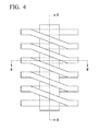
- FIG. 4 is a plan view illustrating a schematic configuration of a thin film flux gate sensor.
- FIG. 5A and FIG. 5B are sectional views of the thin film flux gate sensor illustrated in FIG. 4 .
- FIG. 5A illustrates part A-A of the thin film flux gate sensor illustrated in FIG. 4 .
- FIG. 5B illustrates part B-B of the thin film flux gate sensor illustrated in FIG. 4 .
- the thin film flux gate sensor includes a first wiring layer 1, a first insulating layer 2, a magnetic film 3, a second insulating layer 4, and a second wiring layer 5.
- the thin film flux gate sensor normally includes a protective layer that covers the second wiring layer 5.
- Patent Document 1 A manufacturing method of the thin film flux gate sensor, for example, has been disclosed in Patent Document 1 and Patent Document 2.
- a metal film using aluminum (Al) and the like is formed as the first wiring layer 1.
- an inorganic oxide film using silicon oxide (SiO 2 ) and the like is formed by sputtering or CVD (Chemical Vapor Deposition).
- CVD Chemical Vapor Deposition
- magnetic characteristics are degraded due to unevenness of the first wiring layer 1 serving as a base. Accordingly, after the first insulating layer 2 is thickly formed, a planarization process using etching back method or CMP (Chemical Mechanical Polishing) is needed.
- CMP Chemical Mechanical Polishing
- openings which are for connection to the first wiring layer 1 serving as a base, in the first insulating layer 2 and the second insulating layer 4.
- a resist pattern is formed by photolithography, and then etching is performed by using a method of dry etching and the like. In the case of employing such a process, many man-hours are required and a large-scale manufacturing apparatus is needed. Therefore, the manufacturing cost of the sensor is increased.
- Patent Document 3 has proposed and disclosed a thin film magnetic sensor using a photosensitive polyimide.
- a photosensitive polyimide By employing the photosensitive polyimide, an etching process of the insulating layer is not needed.
- a photosensitive polyimide by coating the photosensitive polyimide, unevenness due to the base wiring is reduced, and the planarization process for the insulating layer is not needed. Therefore, it is possible to manufacture the sensor at a low cost.
- a seed layer is sputtered on a non-magnetic substrate 10 to form a resist mask, electrolytic plating is performed, and then the seed layer is removed by using etching.
- the first wiring layer 1 serving as the lower layer wiring of a solenoid coil is formed.
- the first wiring layer 1 is coated with photosensitive polyimide, and is exposed, developed, and thermally cured. In this way, the first insulating layer 2 with openings 8, through which the wiring of the solenoid coil is connected, is formed.
- the magnetic film 3 is formed by sputtering and liftoff is performed, so that a core including a soft magnetic substance is formed.
- a heat treatment is performed in a rotating magnetic field or a static magnetic field.
- the magnetic film 3 is coated with photosensitive polyimide, and is exposed, developed, and thermally cured.
- the second insulating layer 4 with openings 9, through which the wiring of the solenoid coil is connected is formed.
- a seed layer is sputtered on the second insulating layer 4 to form a resist mask, electrolytic plating is performed, and then the seed layer is removed by using etching.
- the second wiring layer 5 serving as the upper layer wiring of the solenoid coil is formed.
- the second wiring layer 5 is provided with electrodes pad (not illustrated) for connection to terminals.
- a protective film (not illustrated) formed with openings in electrodes portion for connection to an exterior is formed.
- FIG. 7A and FIG. 7B The sensor element manufactured as described above is formed of a solenoid-like excitation coil and a pickup coil. Triangular wave current illustrated in an upper part of FIG. 7A is allowed to flow through the excitation coil.
- a horizontal axis denotes a time t.
- a magnetic field H exc is generated around the excitation coil.
- a middle part of FIG. 7A is a graph illustrating a change in a magnetization of the core excited by the magnetic field H exc of the excitation coil.
- the excitation coil has B-H characteristics illustrated in FIG. 7B .
- the magnetization characteristics of the core are also changed as illustrated in the middle part of FIG. 7A according to the polarity of the external magnetic field H ext .
- a dashed dotted line indicates the case in which H ext >0 and a double dot and dash line indicates the case in which H ext ⁇ 0.
- a temporal position, at which the spike-like voltage is generated at the voltage of the pickup coil, is also changed as illustrated in the lower part of FIG. 7A according to the polarity of the external magnetic field H ext .
- FIG. 7A a temporal position, at which the spike-like voltage is generated at the voltage of the pickup coil
- a dashed dotted line indicates the case in which H ext >0 and a double dot and dash line indicates the case in which H ext ⁇ 0.
- H ext when the external magnetic field H ext is applied (H ext ⁇ 0 or H ext >0), temporally preceding or succeeding shift occurs. Accordingly, from a time interval of spike-like waveforms of the voltage of the pickup coil, the size and direction of the external magnetic field H ext can be recognized.
- Equation (1) a time t 1 is expressed by Equation (1) and a time t 2 is expressed by Equation (2).
- H c denotes coercive force of the excitation coil
- T d denotes a delay time.
- Equation (3) it can be recognized that it is possible to remove the influence of hysteresis caused by the coercive force of the excitation coil. Moreover, digital detection using a counter is possible. Consequently, it is possible to remove the influence of an error at the time of analog/digital conversion. Thereby, it is possible to configure the sensor with good linearity.
- the linearity of sensor output depends on the linearity of a current value of a triangular wave with respect to time and the linearity of magnetic flux density of the core for the excitation magnetic field generated by the excitation coil and the external magnetic field to be detected.
- a generation time interval of a pickup voltage for the external magnetic field is changed along the magnetization curve of the magnetic film.
- a material with good linearity of the magnetization curve be used as a material of the magnetic film.
- a material with good linearity of the magnetization curve for example, there are Co-based amorphous materials such as CoFeSiB, CoNbZr, and CoTaZr, and soft magnetic materials such as NiFe and CoFe.
- Co-based amorphous materials such as CoFeSiB, CoNbZr, and CoTaZr
- soft magnetic materials such as NiFe and CoFe.
- the first insulating layer 2 is formed by using the photosensitive polyimide, and then several processes of applying heat are performed. That is, temperatures in the processes are a film formation temperature when forming the magnetic film 3 (a magnetic layer), a processing temperature of the heat treatment in the magnetic field, and a temperature of the heat curing process for the polyimide when forming the second insulating layer 4.
- temperatures in the processes are a film formation temperature when forming the magnetic film 3 (a magnetic layer), a processing temperature of the heat treatment in the magnetic field, and a temperature of the heat curing process for the polyimide when forming the second insulating layer 4.
- the highest temperature among the heat treatment temperatures in each process will be referred to as a "process temperature.”
- a threshold voltage is provided by a hysteresis comparator and the like to detect a time
- a time interval at which the pickup voltage reaches the threshold voltage is not linear for the external magnetic field, and the linearity of the output characteristics of the sensor is significantly deteriorated.
- the present invention provides a manufacturing method of a flux gate sensor that does not damage the linearity of a magnetization curve of a magnetic layer (a magnetic film).
- a manufacturing method of a flux gate sensor may include at least: a first step of forming a first wiring layer on a substrate; a second step of forming a first insulating layer made of a first resin to cover the first wiring layer; a third step of forming a magnetic layer on the first insulating layer, the magnetic layer constituting a core of a flux gate; a fourth step of forming a second insulating layer made of a second resin on the first insulating layer to cover the magnetic layer; and a fifth step of forming a second wiring layer on the second insulating layer, wherein the first wiring layer and the second wiring layer are electrically connected to each other so that each of the first wiring layer and the second wiring layer constitutes a magnetic coil and a pickup coil, and at least a process temperature in each of the third, fourth, and fifth steps is lower than a glass transition temperature of the first resin.
- the glass transition temperature of the first resin may be higher than 300°C.
- a temperature of the process in the third step may be a higher temperature of a first temperature at a time of formation of the magnetic layer and a second temperature at a time of a heat treatment in a magnetic field which is performed after the magnetic layer is formed.
- the third step may include a first process of forming a cobalt-based amorphous soft magnetic film by a sputtering method, and a second process of performing the heat treatment in the magnetic field and controlling induced magnetic anisotropy in the formed magnetic layer.
- the first and second resins may be the same photosensitive polyimide.
- a heat curing temperature of the first resin may be 350°C to 400°C, and a heat curing temperature of the second resin may be 250°C to 300°C.
- the manufacturing method of the flux gate sensor of the present invention the deterioration of the linearity of the magnetic characteristics caused by an increase in the coercive force of the magnetic film is suppressed, resulting in the obtainment of the flux gate sensor with good output characteristics.
- the manufacturing method of the flux gate sensor of the present invention can be applied regardless of magnitude of the film formation temperature and a temperature of the heat treatment in the magnetic field.
- the manufacturing method of the flux gate sensor of the present invention it is possible to specify the process of forming the magnetic layer. According to the manufacturing method of the flux gate sensor of the present invention, it is possible to employ a resin, which is different from the resin of the second insulating layer and has a high heat curing temperature, as the resin of the first insulating layer.
- FIG. 1 is a flowchart illustrating a procedure of a manufacturing method of a flux gate sensor in accordance with a first preferred embodiment of the present invention.
- a seed layer is sputtered on a non-magnetic substrate to form a photoresist mask, electrolytic plating is performed, and then the seed layer is removed by using etching.
- a first wiring layer 1 serving as a lower layer wiring of a solenoid coil is formed.
- step S2 the first wiring layer 1 is coated with photosensitive polyimide, and is exposed, developed, and thermally cured. In this way, a first insulating layer 2 with openings, through which a wiring of the solenoid coil is connected, is formed.
- Tg glass transition temperature
- step S3 after liftoff resist is formed on the first insulating layer 2, a magnetic film 3 is formed by sputtering, and liftoff is performed. In this way, a core including a soft magnetic substance is formed.
- the film formation temperature when forming the magnetic film 3 is set to be lower than the glass transition temperature (Tg) of the polyimide employed in the first insulating layer 2.
- Tg glass transition temperature
- a Co-based amorphous material such as CoFeSiB, CoNbZr, or CoTaZr
- a soft magnetic material such as NiFe or CoFe are preferable.
- step S4 in order to remove residual stress incidental to the formation of the soft magnetic film, or irregular induced magnetic anisotropy generated due to a magnetic field in a sputtering apparatus, a heat treatment is performed in a rotating magnetic field or a static magnetic field.
- the temperature of the heat treatment in the magnetic field is set to be lower than the glass transition temperature (Tg) of the polyimide employed in the first insulating layer 2.
- FIG. 2 illustrates a relation between a heat treatment temperature in a magnetic field and coercive force in a CoNbZr film formed on two types of polyimide with different glass transition temperatures (Tg).
- FIG. 2 illustrates two types of polyimide A and B and a silicon substrate.
- glass transition temperatures (Tg) of the polyimide A is 350°C
- glass transition temperatures (Tg) of the polyimide B is 320°C.
- the coercive force is increased when the heat treatment temperature in the magnetic field exceeds 350°C.
- the coercive force is increased when the heat treatment temperature in the magnetic field exceeds 320°C. That is, in both cases, when the heat treatment temperature in the magnetic field exceeds the glass transition temperature, the coercive force is increased, and the linearity of the magnetization curve is highly likely to be deteriorated.
- the base polyimide provided with the coercive magnetic film is softened through a heat treatment at a temperature exceeding the glass transition temperature, and an elastic modulus is significantly reduced. Therefore, distortion due to the stress of the magnetic film formed on the base polyimide is very large. Thus, it is considered that anisotropic energy of the magnetic film is increased due to an inverse magnetostriction effect, and coercive force is increased.
- the coercive force is small as it is even when the heat treatment temperature in the magnetic field is 400°C.
- the heat treatment temperature in the magnetic field is set to be less than or equal to 350°C
- the heat treatment temperature in the magnetic field is set to be less than or equal to 320°C.
- the heat treatment temperature in the magnetic field but also temperatures of heat treatments in processes to be performed after the process of forming the magnetic film are preferably lower than the glass transition temperature of the resin employed in the first insulating layer 2.
- step S5 the magnetic film 3 is coated with photosensitive polyimide, and is exposed, developed, and thermally cured. In this way, a second insulating layer 4 with openings, through which the wiring of the solenoid coil is connected, is formed.
- a heat curing temperature at this time is also set to be lower than the glass transition temperature (Tg) of the polyimide employed in the first insulating layer 2.
- Tg glass transition temperature
- the heat curing process suppresses a change in the characteristics of the magnetic film caused by heat, it is preferable to perform the heat curing process in the state in which a rotating magnetic field or a static magnetic field has been applied.
- step S6 similarly to the first wiring layer 1, a seed layer is sputtered on the second insulating layer 4 to form a resist mask, electrolytic plating is performed, and then the seed layer is removed by using etching. In this way, a second wiring layer 5 serving as the upper layer wiring of the solenoid coil is formed.
- the second wiring layer 5 is provided with an electrode pad (not illustrated) for connection to an exterior.
- a protective film (not illustrated) with openings, which is in the electrode portion for connection to an exterior, is formed.
- a heat curing temperature thereof is also set to be lower than the glass transition temperature (Tg) of the polyimide employed in the first insulating layer 2, and it is preferable that a process thereof is performed in the state in which a rotating magnetic field or a static magnetic field has been applied.
- configuration A in which the first wiring layer 1 serving as the lower layer wiring of the solenoid coil and the second wiring layer 5 serving as the upper layer wiring of the solenoid coil are electrically connected to each other through the openings formed in each of the first insulating layer 2 and the second insulating layer 4, has been described in detail.
- configuration A it may be possible to employ a configuration in which an insulating layer including the first insulating layer 2 and the second insulating layer 4 is provided only in an inner space of the solenoid coil including the first wiring layer 1 and the second wiring layer 5, and the magnetic film 3 is included in the first insulating layer 2 and the second insulating layer 4. That is, it may be possible to employ a configuration (not illustrated; hereinafter referred to as a "configuration B") in which the second wiring layer 5 is provided along outer peripheral surfaces of the first insulating layer 2 and the second insulating layer 4 stacked on the first insulating layer 2, and is electrically connected to the first wiring layer 1.
- the configuration B may be obtained by forming the first insulating layer 2 and the second insulating layer 4 such that both ends of the first wiring layer 1 are exposed, then forming the resist mask in step S6 on the second insulating layer 4 and the first wiring layer 1, then performing electrolytic plating, and then removing the seed by etching.
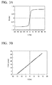
- FIG. 3A For the flux gate sensor employing Co 85 Nb 12 Zr 3 as a material of the magnetic film and manufactured based on the above-described manufacturing method, a magnetization curve (a B-H curve) of the magnetic film after the manufacturing process is performed is illustrated in FIG. 3A . As illustrated in FIG. 3A , good linearity is maintained. Furthermore, the output characteristics of the sensor at this time are illustrated in FIG. 3B . As illustrated in FIG. 3B , when the linearity of the magnetic film is maintained, good output characteristics are maintained.
- the film formation temperature, a processing temperature of the heat treatment in the magnetic field, the processing temperature of the heat curing process of the second insulating layer, and the like are set to be lower than the glass transition temperature (Tg) of the polyimide employed in the first insulating layer, so that the deterioration of the linearity of the magnetic characteristics caused by an increase in the coercive force of the magnetic film is suppressed, and a flux gate sensor with good output characteristics can be obtained.
- the heat curing temperature of the polyimide is low, since it is difficult to sufficiently ensure resistance to a chemical solution in a process, the heat curing temperature is preferably about 250°C to about 300°C.
- a solder reflow temperature at the time of an assembly process of a sensor module or mounting of the sensor on the substrate is about 260°C.
- the glass transition temperature of the resin employed in the first insulating layer is lower than the solder reflow temperature, since the coercive force of the magnetic film is increased by heating at the time of solder reflow, the linearity of the magnetic characteristics of the sensor is deteriorated. Accordingly, it is preferable that the glass transition temperature of the resin employed in the first insulating layer be sufficiently higher than the solder reflow temperature.
- the glass transition temperature (Tg) of the polyimide employed in the first insulating layer be greater than or equal to 300°C. That is, the flux gate sensor with superior resistance to the reflow temperature and good output characteristics is obtained.
- Tg glass transition temperature
- the above-described preferred embodiment is an example, and various embodiments for realizing the scope of the present invention can be made by those skilled in the art.
- the photosensitive polyimide is employed as the insulating layer has been described.
- the present invention is not limited thereto.
- it may be possible to employ a photosensitive resin material such as polybenzoxazole or cresol novalac resin.
- the first insulating layer and the second insulating layer are preferably made of the same material. Accordingly, from the above description, in such a case, a material is used that the glass transition temperature (Tg) thereof is greater than or equal to 300°C, and a heat curable temperature thereof is a temperature of about 250°C to about 300°C.
- a heat curing temperature for the material employed in the first insulating layer is preferably about 350°C to about 400°C.
- the photosensitive polyimide which is a photosensitive material
- non-photosensitive polyimide may be employed if pattern formation is possible by a micro fabrication process such as photolithography or nanoimprint.
- the non-photosensitive polyimide generally has a higher glass transition temperature than the photosensitive polyimide, and a non-photosensitive polyimide with a glass transition temperature of about 400°C also exists. Accordingly, in the case of employing the non-photosensitive polyimide, it is possible to set the temperature limited in the present invention to about 400°C.
- the electrolytic plating method is used as the wiring formation method.
- the wirings may be formed by etching a conductive material such as aluminum (Al), gold (Au), or copper (Cu) formed using electroless plating or sputtering.
- the manufacturing method of the present invention can be applied to a thin film flux gate sensor employed in an electronic azimuth meter used in a cellular phone and the like. Furthermore, the manufacturing method of the present invention can be applied to a current sensor that detects a magnetic field generated by a current to measure a current value, a magnetic rotary encoder, or a thin film flux gate sensor employed in a linear encoder. Furthermore, the manufacturing method of the present invention can be applied to a thin film flux gate sensor employed in an apparatus that detects magnetic particles including a magnetic material or foreign substances.
Landscapes
- Physics & Mathematics (AREA)
- Engineering & Computer Science (AREA)
- Condensed Matter Physics & Semiconductors (AREA)
- General Physics & Mathematics (AREA)
- Manufacturing & Machinery (AREA)
- Microelectronics & Electronic Packaging (AREA)
- Measuring Magnetic Variables (AREA)
- Hall/Mr Elements (AREA)
Abstract
Provided is a manufacturing method of a flux gate sensor comprising at least: a first step of forming a first wiring layer on a substrate; a second step of forming a first insulating layer made of a first resin to cover the first wiring layer; a third step of forming a magnetic layer on the first insulating layer, the magnetic layer constituting a core of a flux gate; a fourth step of forming a second insulating layer made of a second resin on the first insulating layer to cover the magnetic layer; and a fifth step of forming a second wiring layer on the second insulating layer, wherein the first wiring layer and the second wiring layer are electrically connected to each other so that each of the first wiring layer and the second wiring layer constitutes a magnetic coil and a pickup coil, and at least a process temperature in each of the third, fourth, and fifth steps is lower than a glass transition temperature of the first resin.
Description
- The present invention relates to a manufacturing method of a flux gate sensor. Specifically, the present invention relates to a manufacturing method of a thin film flux gate sensor employed in an electronic azimuth meter used in a cellular phone and the like.
Priority is claimed on Japanese Patent Application No.2010-110229, filed May 12, 2010 - An electronic azimuth meter has been used in a cellular phone, a portable navigation device, a game controller and the like. In order to miniaturize the entirety of an apparatus, demands for the electronic azimuth meter to achieve a small size and integration have been increasing. In order to achieve the small size and integration, replacing a sensor used in the electronic azimuth meter with a thin film flux gate sensor has been considered.
-
FIG. 4 is a plan view illustrating a schematic configuration of a thin film flux gate sensor.FIG. 5A and FIG. 5B are sectional views of the thin film flux gate sensor illustrated inFIG. 4 .FIG. 5A illustrates part A-A of the thin film flux gate sensor illustrated inFIG. 4 .FIG. 5B illustrates part B-B of the thin film flux gate sensor illustrated inFIG. 4 .
As illustrated inFIG. 4 ,FIG. 5A, and FIG. 5B , the thin film flux gate sensor includes afirst wiring layer 1, a firstinsulating layer 2, amagnetic film 3, a secondinsulating layer 4, and asecond wiring layer 5. In addition, although not illustrated in the figures, the thin film flux gate sensor normally includes a protective layer that covers thesecond wiring layer 5. - A manufacturing method of the thin film flux gate sensor, for example, has been disclosed in
Patent Document 1 andPatent Document 2. In the manufacturing methods disclosed in these Patent Documents, a metal film using aluminum (Al) and the like is formed as thefirst wiring layer 1. Then, as the firstinsulating layer 2, an inorganic oxide film using silicon oxide (SiO2) and the like is formed by sputtering or CVD (Chemical Vapor Deposition). At this time, magnetic characteristics are degraded due to unevenness of thefirst wiring layer 1 serving as a base. Accordingly, after the firstinsulating layer 2 is thickly formed, a planarization process using etching back method or CMP (Chemical Mechanical Polishing) is needed. Furthermore, it is necessary to provide openings, which are for connection to thefirst wiring layer 1 serving as a base, in the firstinsulating layer 2 and the secondinsulating layer 4. A resist pattern is formed by photolithography, and then etching is performed by using a method of dry etching and the like. In the case of employing such a process, many man-hours are required and a large-scale manufacturing apparatus is needed. Therefore, the manufacturing cost of the sensor is increased. - In this regard, for example,
Patent Document 3 has proposed and disclosed a thin film magnetic sensor using a photosensitive polyimide. By employing the photosensitive polyimide, an etching process of the insulating layer is not needed. Moreover, by coating the photosensitive polyimide, unevenness due to the base wiring is reduced, and the planarization process for the insulating layer is not needed. Therefore, it is possible to manufacture the sensor at a low cost. - Hereinafter, the manufacturing method of the thin film flux gate sensor configured as above will be schematically described with reference to
FIG. 6A to FIG. 6E .
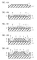
First, as illustrated inFIG. 6A , a seed layer is sputtered on anon-magnetic substrate 10 to form a resist mask, electrolytic plating is performed, and then the seed layer is removed by using etching. In this way, thefirst wiring layer 1 serving as the lower layer wiring of a solenoid coil is formed.
Next, as illustrated inFIG. 6B , thefirst wiring layer 1 is coated with photosensitive polyimide, and is exposed, developed, and thermally cured. In this way, the firstinsulating layer 2 withopenings 8, through which the wiring of the solenoid coil is connected, is formed.
Moreover, as illustrated inFIG. 6C , after liftoff resist is formed on the first insulatinglayer 2, themagnetic film 3 is formed by sputtering and liftoff is performed, so that a core including a soft magnetic substance is formed.
Next, in order to remove residual stress incidental to the formation of the soft magnetic film, or irregular induced magnetic anisotropy generated due to a magnetic field in a sputtering apparatus, a heat treatment is performed in a rotating magnetic field or a static magnetic field. - Moreover, as illustrated in
FIG. 6D , themagnetic film 3 is coated with photosensitive polyimide, and is exposed, developed, and thermally cured. In this way, the secondinsulating layer 4 withopenings 9, through which the wiring of the solenoid coil is connected, is formed.
Subsequently, as illustrated inFIG. 6E , similarly to thefirst wiring layer 1, a seed layer is sputtered on the secondinsulating layer 4 to form a resist mask, electrolytic plating is performed, and then the seed layer is removed by using etching. In this way, thesecond wiring layer 5 serving as the upper layer wiring of the solenoid coil is formed. In addition, thesecond wiring layer 5 is provided with electrodes pad (not illustrated) for connection to terminals.
Finally, a protective film (not illustrated) formed with openings in electrodes portion for connection to an exterior is formed. - Here, the main point of an operation principle of the thin film flux gate sensor manufactured in the above procedure will be described with reference to
FIG. 7A and FIG. 7B .
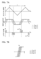
The sensor element manufactured as described above is formed of a solenoid-like excitation coil and a pickup coil. Triangular wave current illustrated in an upper part ofFIG. 7A is allowed to flow through the excitation coil. InFIG. 7A , a horizontal axis denotes a time t. In this way, a magnetic field Hexc is generated around the excitation coil. A middle part ofFIG. 7A is a graph illustrating a change in a magnetization of the core excited by the magnetic field Hexc of the excitation coil. Here, the excitation coil has B-H characteristics illustrated inFIG. 7B . When an excitation current is above or below a constant value according to the B-H characteristics, the magnetization is saturated and reaches the constant value. At this time, as illustrated in a lower part ofFIG. 7A , at a zero cross point of the magnetization in the core, a spike-like voltage is generated at the pickup coil. - Here, when no external magnetic field Hext is applied (Hext=0), the magnetization of the core is indicated by a solid line of the middle part of
FIG. 7A . The voltage of the pickup coil is indicated by a solid line of the low part ofFIG. 7A .
Next, the case in which the external magnetic field Hext is applied (Hext<0 or Hext>0) is considered. At this time, the magnetization characteristics are also changed as illustrated inFIG. 7B according to the polarity of the external magnetic field Hext. InFIG. 7B , a dashed dotted line indicates the case in which Hext>0 and a double dot and dash line indicates the case in which Hext<0. Accordingly, the magnetization characteristics of the core are also changed as illustrated in the middle part ofFIG. 7A according to the polarity of the external magnetic field Hext. In the middle part ofFIG. 7A , a dashed dotted line indicates the case in which Hext>0 and a double dot and dash line indicates the case in which Hext<0. Moreover, a temporal position, at which the spike-like voltage is generated at the voltage of the pickup coil, is also changed as illustrated in the lower part ofFIG. 7A according to the polarity of the external magnetic field Hext. In the lower part ofFIG. 7A , similarly to the above, a dashed dotted line indicates the case in which Hext>0 and a double dot and dash line indicates the case in which Hext<0. As compared with the case in which no external magnetic field is applied, when the external magnetic field Hext is applied (Hext<0 or Hext>0), temporally preceding or succeeding shift occurs. Accordingly, from a time interval of spike-like waveforms of the voltage of the pickup coil, the size and direction of the external magnetic field Hext can be recognized. - At this time, in the lower part of
FIG. 7A , a time t1 is expressed by Equation (1) and a time t2 is expressed by Equation (2). In Equation (1) and (2), Hc denotes coercive force of the excitation coil and Td denotes a delay time. Thus, when (t2-t1) is calculated, so that Equation (3) is obtained. -

- From Equation (3), it can be recognized that it is possible to remove the influence of hysteresis caused by the coercive force of the excitation coil. Moreover, digital detection using a counter is possible. Consequently, it is possible to remove the influence of an error at the time of analog/digital conversion. Thereby, it is possible to configure the sensor with good linearity.
- At this time, the linearity of sensor output depends on the linearity of a current value of a triangular wave with respect to time and the linearity of magnetic flux density of the core for the excitation magnetic field generated by the excitation coil and the external magnetic field to be detected. A generation time interval of a pickup voltage for the external magnetic field is changed along the magnetization curve of the magnetic film. Thus, deterioration of the linearity of the magnetization curve directly affects deterioration of the linearity of the sensor output.
- Accordingly, it is said that the coercive force is theoretically offset, but it is preferable that a material with good linearity of the magnetization curve be used as a material of the magnetic film. As such a material, for example, there are Co-based amorphous materials such as CoFeSiB, CoNbZr, and CoTaZr, and soft magnetic materials such as NiFe and CoFe. As described above, when the soft magnetic substance with good linearity of the magnetization curve is used in the core, a sensor element with good linearity is obtained.
-
- Patent Document 1: Japanese Patent Publication No.
2730467 - Patent Document 2:
PCT International Publication No. WO 2007-126164 - Patent Document 3: Japanese Unexamined Patent Application, First Publication, No.
2008-275578 - In the manufacturing process of the sensor, as described above, the first insulating
layer 2 is formed by using the photosensitive polyimide, and then several processes of applying heat are performed. That is, temperatures in the processes are a film formation temperature when forming the magnetic film 3 (a magnetic layer), a processing temperature of the heat treatment in the magnetic field, and a temperature of the heat curing process for the polyimide when forming the second insulatinglayer 4. In addition, hereinafter, the highest temperature among the heat treatment temperatures in each process will be referred to as a "process temperature." - Here, when these heat treatment temperatures are higher than a glass transition temperature (Tg) of the first insulating
layer 2 of the polyimide serving as the base on which the magnetic film is formed, the polyimide is contracted and modified, and themagnetic film 3 formed on the first insulating layer is also modified. As a consequence, since a stress state of themagnetic film 3 is changed, the characteristics of themagnetic film 3 are degraded. That is, as illustrated in a magnetization curve (a B-H curve) ofFIG. 8 , as coercive force is increased, the linearity of the magnetization curve is deteriorated. Furthermore, the linearity of output characteristics of a sensor using the magnetic film with the deteriorated linearity of the magnetization curve as described above is also deteriorated. - In the sensor with a deteriorated linearity of the output characteristics, particularly, in the case in which positive and negative magnetic fields are alternately applied as with an excitation magnetic field, changes in magnetic flux densities are different from each other when positive and negative magnetic fields are alternately applied such as the positive magnetic field is applied and then the negative magnetic field is applied or the negative magnetic field is applied and then the positive magnetic field is applied. Accordingly, the waveform of the pickup voltage when external magnetic fields are overlapped may be easily distorted. Furthermore, in the case in which a threshold voltage is provided by a hysteresis comparator and the like to detect a time, when waveform distortion becomes large by applying an external magnetic field, a time interval at which the pickup voltage reaches the threshold voltage is not linear for the external magnetic field, and the linearity of the output characteristics of the sensor is significantly deteriorated.
- The present invention provides a manufacturing method of a flux gate sensor that does not damage the linearity of a magnetization curve of a magnetic layer (a magnetic film).
- A manufacturing method of a flux gate sensor may include at least: a first step of forming a first wiring layer on a substrate; a second step of forming a first insulating layer made of a first resin to cover the first wiring layer; a third step of forming a magnetic layer on the first insulating layer, the magnetic layer constituting a core of a flux gate; a fourth step of forming a second insulating layer made of a second resin on the first insulating layer to cover the magnetic layer; and a fifth step of forming a second wiring layer on the second insulating layer, wherein the first wiring layer and the second wiring layer are electrically connected to each other so that each of the first wiring layer and the second wiring layer constitutes a magnetic coil and a pickup coil, and at least a process temperature in each of the third, fourth, and fifth steps is lower than a glass transition temperature of the first resin.
- The glass transition temperature of the first resin may be higher than 300°C.
- A temperature of the process in the third step may be a higher temperature of a first temperature at a time of formation of the magnetic layer and a second temperature at a time of a heat treatment in a magnetic field which is performed after the magnetic layer is formed.
- The third step may include a first process of forming a cobalt-based amorphous soft magnetic film by a sputtering method, and a second process of performing the heat treatment in the magnetic field and controlling induced magnetic anisotropy in the formed magnetic layer.
- The first and second resins may be the same photosensitive polyimide. A heat curing temperature of the first resin may be 350°C to 400°C, and a heat curing temperature of the second resin may be 250°C to 300°C.
- According to the manufacturing method of the flux gate sensor of the present invention, the deterioration of the linearity of the magnetic characteristics caused by an increase in the coercive force of the magnetic film is suppressed, resulting in the obtainment of the flux gate sensor with good output characteristics.
According to the manufacturing method of the flux gate sensor of the present invention, it is also possible to exclude the influence of the heat curing temperature when forming the second insulating layer.
According to the manufacturing method of the flux gate sensor of the present invention, it is possible to employ a temperature (250°C to 300°C) sufficient as the heat curing temperature when forming the second insulating layer.
The manufacturing method of the flux gate sensor of the present invention can be applied regardless of magnitude of the film formation temperature and a temperature of the heat treatment in the magnetic field.
According to the manufacturing method of the flux gate sensor of the present invention, it is possible to specify the process of forming the magnetic layer.
According to the manufacturing method of the flux gate sensor of the present invention, it is possible to employ a resin, which is different from the resin of the second insulating layer and has a high heat curing temperature, as the resin of the first insulating layer. -
-
FIG. 1 is a flowchart illustrating a procedure in a manufacturing method of a flux gate sensor in accordance with a first preferred embodiment of the present invention. -
FIG. 2 is a diagram illustrating a relation between a heat treatment temperature in a magnetic field and coercive force in a CoNbZr film formed on two types of polyimide with different glass transition temperatures (Tg). -
FIG. 3A is a diagram illustrating a magnetization curve of a magnetic film of a flux gate sensor obtained by a manufacturing method in accordance with the first preferred embodiment of the present invention. -
FIG. 3B is a diagram illustrating output characteristics of a flux gate sensor obtained by a manufacturing method in accordance with the first preferred embodiment of the present invention. -
FIG. 4 is a plan view illustrating a schematic configuration of a thin film flux gate sensor. -
FIG. 5A is a sectional view of a thin film flux gate sensor illustrated inFIG. 4 . -
FIG. 5B is a sectional view of a thin film flux gate sensor illustrated inFIG. 4 . -
FIG. 6A is a diagram for describing a manufacturing process of a thin film flux gate sensor. -
FIG. 6B is a diagram for describing a manufacturing process of a thin film flux gate sensor. -
FIG. 6C is a diagram for describing a manufacturing process of a thin film flux gate sensor. -
FIG. 6D is a diagram for describing a manufacturing process of a thin film flux gate sensor. -
FIG. 6E is a diagram for describing a manufacturing process of a thin film flux gate sensor. -
FIG. 7A is a diagram for describing the main point of an operation principle. -
FIG. 7B is a diagram for describing the main point of an operation principle. -
FIG. 8 is a diagram for describing problems of a thin film flux gate sensor in accordance with the related art. - Hereinafter, preferred embodiments of the present invention will be described with reference to the accompanying drawings.
In the following description, the highest temperature among temperatures to be applied in each process (step) will be referred to as a "process temperature."
FIG. 1 is a flowchart illustrating a procedure of a manufacturing method of a flux gate sensor in accordance with a first preferred embodiment of the present invention.
According to the manufacturing method in accordance with the first preferred embodiment of the present invention, first, in step S1, a seed layer is sputtered on a non-magnetic substrate to form a photoresist mask, electrolytic plating is performed, and then the seed layer is removed by using etching. In this way, afirst wiring layer 1 serving as a lower layer wiring of a solenoid coil is formed. - Next, in step S2, the
first wiring layer 1 is coated with photosensitive polyimide, and is exposed, developed, and thermally cured. In this way, a first insulatinglayer 2 with openings, through which a wiring of the solenoid coil is connected, is formed. The higher a heat curing temperature at this time is, the higher a glass transition temperature (Tg) of the polyimide is. A temperature of about 350°C to about 400°C is preferable since pyrolysis of the polyimide starts at a temperature greater than or equal to about 400°C. - Next, in step S3, after liftoff resist is formed on the first insulating
layer 2, amagnetic film 3 is formed by sputtering, and liftoff is performed. In this way, a core including a soft magnetic substance is formed. In the first preferred embodiment of the present invention, the film formation temperature when forming themagnetic film 3 is set to be lower than the glass transition temperature (Tg) of the polyimide employed in the first insulatinglayer 2. In addition, as themagnetic film 3 used at this time, a Co-based amorphous material such as CoFeSiB, CoNbZr, or CoTaZr, and a soft magnetic material such as NiFe or CoFe are preferable. - Next, in step S4, in order to remove residual stress incidental to the formation of the soft magnetic film, or irregular induced magnetic anisotropy generated due to a magnetic field in a sputtering apparatus, a heat treatment is performed in a rotating magnetic field or a static magnetic field. In the first preferred embodiment of the present invention, similarly to step S3, the temperature of the heat treatment in the magnetic field is set to be lower than the glass transition temperature (Tg) of the polyimide employed in the first insulating
layer 2. -
FIG. 2 illustrates a relation between a heat treatment temperature in a magnetic field and coercive force in a CoNbZr film formed on two types of polyimide with different glass transition temperatures (Tg).FIG. 2 illustrates two types of polyimide A and B and a silicon substrate. InFIG. 2 , glass transition temperatures (Tg) of the polyimide A is 350°C, and glass transition temperatures (Tg) of the polyimide B is 320°C. - As illustrated in
FIG. 2 , in the case of the polyimide A, the coercive force is increased when the heat treatment temperature in the magnetic field exceeds 350°C. In the case of the polyimide B, the coercive force is increased when the heat treatment temperature in the magnetic field exceeds 320°C. That is, in both cases, when the heat treatment temperature in the magnetic field exceeds the glass transition temperature, the coercive force is increased, and the linearity of the magnetization curve is highly likely to be deteriorated. The base polyimide provided with the coercive magnetic film is softened through a heat treatment at a temperature exceeding the glass transition temperature, and an elastic modulus is significantly reduced. Therefore, distortion due to the stress of the magnetic film formed on the base polyimide is very large. Thus, it is considered that anisotropic energy of the magnetic film is increased due to an inverse magnetostriction effect, and coercive force is increased. - In addition, in the case in which a CoNbZr film is formed on the silicon substrate, the coercive force is small as it is even when the heat treatment temperature in the magnetic field is 400°C.
From the above, for example, in the case of employing the polyimide A, the heat treatment temperature in the magnetic field is set to be less than or equal to 350°C, and in the case of employing the polyimide B, the heat treatment temperature in the magnetic field is set to be less than or equal to 320°C. In this way, it is possible to suppress an increase in the coercive force in the magnetization curve of the magnetic film, and the deterioration of linearity is suppressed. Furthermore, since the increase in the coercive force is caused due to the above reasons, not only the heat treatment temperature in the magnetic field but also temperatures of heat treatments in processes to be performed after the process of forming the magnetic film are preferably lower than the glass transition temperature of the resin employed in the first insulatinglayer 2. - Returning to the procedure of the manufacturing method of
FIG. 1 , in step S5, themagnetic film 3 is coated with photosensitive polyimide, and is exposed, developed, and thermally cured. In this way, a secondinsulating layer 4 with openings, through which the wiring of the solenoid coil is connected, is formed. In the first preferred embodiment of the present invention, a heat curing temperature at this time is also set to be lower than the glass transition temperature (Tg) of the polyimide employed in the first insulatinglayer 2. In addition, since the heat curing process suppresses a change in the characteristics of the magnetic film caused by heat, it is preferable to perform the heat curing process in the state in which a rotating magnetic field or a static magnetic field has been applied. - Subsequently, in step S6, similarly to the
first wiring layer 1, a seed layer is sputtered on the second insulatinglayer 4 to form a resist mask, electrolytic plating is performed, and then the seed layer is removed by using etching. In this way, asecond wiring layer 5 serving as the upper layer wiring of the solenoid coil is formed. In addition, thesecond wiring layer 5 is provided with an electrode pad (not illustrated) for connection to an exterior. - Finally, in step S7, a protective film (not illustrated) with openings, which is in the electrode portion for connection to an exterior, is formed. In addition, even when forming the protective film, it is preferable that a heat curing temperature thereof is also set to be lower than the glass transition temperature (Tg) of the polyimide employed in the first insulating
layer 2, and it is preferable that a process thereof is performed in the state in which a rotating magnetic field or a static magnetic field has been applied. - Based on
FIG. 1 , in the above-mentioned manufacturing method, the configuration (hereinafter, referred to as a "configuration A"), in which thefirst wiring layer 1 serving as the lower layer wiring of the solenoid coil and thesecond wiring layer 5 serving as the upper layer wiring of the solenoid coil are electrically connected to each other through the openings formed in each of the first insulatinglayer 2 and the second insulatinglayer 4, has been described in detail. However, instead of the configuration A, it may be possible to employ a configuration in which an insulating layer including the first insulatinglayer 2 and the second insulatinglayer 4 is provided only in an inner space of the solenoid coil including thefirst wiring layer 1 and thesecond wiring layer 5, and themagnetic film 3 is included in the first insulatinglayer 2 and the second insulatinglayer 4. That is, it may be possible to employ a configuration (not illustrated; hereinafter referred to as a "configuration B") in which thesecond wiring layer 5 is provided along outer peripheral surfaces of the first insulatinglayer 2 and the second insulatinglayer 4 stacked on the first insulatinglayer 2, and is electrically connected to thefirst wiring layer 1. The configuration B, for example, may be obtained by forming the first insulatinglayer 2 and the second insulatinglayer 4 such that both ends of thefirst wiring layer 1 are exposed, then forming the resist mask in step S6 on the second insulatinglayer 4 and thefirst wiring layer 1, then performing electrolytic plating, and then removing the seed by etching. - For the flux gate sensor employing Co85Nb12Zr3 as a material of the magnetic film and manufactured based on the above-described manufacturing method, a magnetization curve (a B-H curve) of the magnetic film after the manufacturing process is performed is illustrated in
FIG. 3A . As illustrated inFIG. 3A , good linearity is maintained. Furthermore, the output characteristics of the sensor at this time are illustrated inFIG. 3B . As illustrated inFIG. 3B , when the linearity of the magnetic film is maintained, good output characteristics are maintained. - As described above, the film formation temperature, a processing temperature of the heat treatment in the magnetic field, the processing temperature of the heat curing process of the second insulating layer, and the like are set to be lower than the glass transition temperature (Tg) of the polyimide employed in the first insulating layer, so that the deterioration of the linearity of the magnetic characteristics caused by an increase in the coercive force of the magnetic film is suppressed, and a flux gate sensor with good output characteristics can be obtained.
In addition, when the heat curing temperature of the polyimide is low, since it is difficult to sufficiently ensure resistance to a chemical solution in a process, the heat curing temperature is preferably about 250°C to about 300°C. Furthermore, a solder reflow temperature at the time of an assembly process of a sensor module or mounting of the sensor on the substrate is about 260°C. When the glass transition temperature of the resin employed in the first insulating layer is lower than the solder reflow temperature, since the coercive force of the magnetic film is increased by heating at the time of solder reflow, the linearity of the magnetic characteristics of the sensor is deteriorated. Accordingly, it is preferable that the glass transition temperature of the resin employed in the first insulating layer be sufficiently higher than the solder reflow temperature. - Thus, from these limitations, it is suitable that the glass transition temperature (Tg) of the polyimide employed in the first insulating layer be greater than or equal to 300°C. That is, the flux gate sensor with superior resistance to the reflow temperature and good output characteristics is obtained.
In addition, the above-described preferred embodiment is an example, and various embodiments for realizing the scope of the present invention can be made by those skilled in the art.
For example, in the above-described preferred embodiment, the case in which the photosensitive polyimide is employed as the insulating layer has been described. However, the present invention is not limited thereto. For example, it may be possible to employ a photosensitive resin material such as polybenzoxazole or cresol novalac resin. - However, in terms of material management in a process, the first insulating layer and the second insulating layer are preferably made of the same material. Accordingly, from the above description, in such a case, a material is used that the glass transition temperature (Tg) thereof is greater than or equal to 300°C, and a heat curable temperature thereof is a temperature of about 250°C to about 300°C. Here, as described in step S2, a heat curing temperature for the material employed in the first insulating layer is preferably about 350°C to about 400°C.
- Furthermore, in the abovementioned embodiment, the photosensitive polyimide, which is a photosensitive material, has been described. However, non-photosensitive polyimide may be employed if pattern formation is possible by a micro fabrication process such as photolithography or nanoimprint. The non-photosensitive polyimide generally has a higher glass transition temperature than the photosensitive polyimide, and a non-photosensitive polyimide with a glass transition temperature of about 400°C also exists. Accordingly, in the case of employing the non-photosensitive polyimide, it is possible to set the temperature limited in the present invention to about 400°C.
- Furthermore, in the above-described preferred embodiment, the electrolytic plating method is used as the wiring formation method. However, the wirings may be formed by etching a conductive material such as aluminum (Al), gold (Au), or copper (Cu) formed using electroless plating or sputtering.
- While preferred embodiments of the present invention have been described and illustrated above, it should be understood that these are examples of the present invention and are not to be considered as limiting. Additions, omissions, substitutions, and other modifications can be made without departing from the scope of the present invention. Accordingly, the present invention is not to be considered as being limited by the foregoing description, and is only limited by the scope of the claims.
- The manufacturing method of the present invention can be applied to a thin film flux gate sensor employed in an electronic azimuth meter used in a cellular phone and the like. Furthermore, the manufacturing method of the present invention can be applied to a current sensor that detects a magnetic field generated by a current to measure a current value, a magnetic rotary encoder, or a thin film flux gate sensor employed in a linear encoder. Furthermore, the manufacturing method of the present invention can be applied to a thin film flux gate sensor employed in an apparatus that detects magnetic particles including a magnetic material or foreign substances.
-
- 1
- first wiring layer
- 2
- first insulating layer
- 3
- magnetic layer (magnetic film)
- 4
- second insulating layer
- 5
- second wiring layer
- 8
- opening
- 9
- opening
- 10
- non-magnetic substrate
Claims (5)
- A manufacturing method of a flux gate sensor comprising at least:a first step of forming a first wiring layer on a substrate;a second step of forming a first insulating layer made of a first resin to cover the first wiring layer;a third step of forming a magnetic layer on the first insulating layer, the magnetic layer constituting a core of a flux gate;a fourth step of forming a second insulating layer made of a second resin on the first insulating layer to cover the magnetic layer; anda fifth step of forming a second wiring layer on the second insulating layer,wherein the first wiring layer and the second wiring layer are electrically connected to each other so that each of the first wiring layer and the second wiring layer constitutes a magnetic coil and a pickup coil, andat least a process temperature in each of the third, fourth, and fifth steps is lower than a glass transition temperature of the first resin.
- The manufacturing method of a flux gate sensor according to claim 1, wherein the glass transition temperature of the first resin is higher than 300°C.
- The manufacturing method of a flux gate sensor according to claim 1, wherein a temperature of the process in the third step is a higher temperature of a first temperature at a time of formation of the magnetic layer and a second temperature at a time of a heat treatment in a magnetic field which is performed after the magnetic layer is formed.
- The manufacturing method of a flux gate sensor according to claim 2, wherein the third step includes a first process of forming a cobalt-based soft magnetic film by a sputtering method, and a second process of performing the heat treatment in the magnetic field and controlling induced magnetic anisotropy in the formed magnetic layer.
- The manufacturing method of a flux gate sensor according to any one of claims 1 to 4, wherein the first and second resins are the same photosensitive polyimide, a heat curing temperature of the first resin is 350°C to 400°C, and a heat curing temperature of the second resin is 250°C to 300°C.
Applications Claiming Priority (2)
| Application Number | Priority Date | Filing Date | Title |
|---|---|---|---|
| JP2010110229 | 2010-05-12 | ||
| PCT/JP2011/060939 WO2011142416A1 (en) | 2010-05-12 | 2011-05-12 | Method for manufacturing flux gate sensor |
Publications (1)
| Publication Number | Publication Date |
|---|---|
| EP2557429A1 true EP2557429A1 (en) | 2013-02-13 |
Family
ID=44914468
Family Applications (1)
| Application Number | Title | Priority Date | Filing Date |
|---|---|---|---|
| EP11780673A Withdrawn EP2557429A1 (en) | 2010-05-12 | 2011-05-12 | Method for manufacturing flux gate sensor |
Country Status (4)
| Country | Link |
|---|---|
| US (1) | US20130064991A1 (en) |
| EP (1) | EP2557429A1 (en) |
| JP (1) | JP5625053B2 (en) |
| WO (1) | WO2011142416A1 (en) |
Families Citing this family (3)
| Publication number | Priority date | Publication date | Assignee | Title |
|---|---|---|---|---|
| JP2014224741A (en) * | 2013-05-16 | 2014-12-04 | 国立大学法人豊橋技術科学大学 | Magnetic particulate detecting device and magnetic particulate detecting method |
| US20170234942A1 (en) * | 2016-02-11 | 2017-08-17 | Texas Instruments Incorporated | Layouts for interlevel crack prevention in fluxgate technology manufacturing |
| CN119446714B (en) * | 2024-09-27 | 2025-11-04 | 北京科技大学 | A coreless arched MEMS inductor and its fabrication method |
Family Cites Families (7)
| Publication number | Priority date | Publication date | Assignee | Title |
|---|---|---|---|---|
| US4933209A (en) * | 1989-06-28 | 1990-06-12 | Hewlett-Packard Company | Method of making a thin film recording head apparatus utilizing polyimide films |
| JP2730467B2 (en) | 1993-12-27 | 1998-03-25 | 株式会社島津製作所 | Magnetic sensor |
| KR100467839B1 (en) * | 2002-03-09 | 2005-01-24 | 삼성전기주식회사 | A weak-magnetic field sensor using printed circuit board and its making method |
| US7535221B2 (en) * | 2006-03-17 | 2009-05-19 | Citizen Holdings Co., Ltd. | Magnetic sensor element and electronic directional measuring device |
| JP2009535616A (en) | 2006-04-28 | 2009-10-01 | マイクロゲート インコーポレイテッド | Thin film type triaxial fluxgate and manufacturing method thereof |
| JP2008275578A (en) * | 2007-04-05 | 2008-11-13 | Fujikura Ltd | Magnetic sensor and manufacturing method thereof |
| TWI438460B (en) * | 2009-05-21 | 2014-05-21 | Fujikura Ltd | Fluxgate sensor and electronic compass using the same |
-
2011
- 2011-05-12 EP EP11780673A patent/EP2557429A1/en not_active Withdrawn
- 2011-05-12 JP JP2012514828A patent/JP5625053B2/en not_active Expired - Fee Related
- 2011-05-12 WO PCT/JP2011/060939 patent/WO2011142416A1/en not_active Ceased
-
2012
- 2012-11-07 US US13/671,035 patent/US20130064991A1/en not_active Abandoned
Non-Patent Citations (1)
| Title |
|---|
| See references of WO2011142416A1 * |
Also Published As
| Publication number | Publication date |
|---|---|
| WO2011142416A1 (en) | 2011-11-17 |
| US20130064991A1 (en) | 2013-03-14 |
| JP5625053B2 (en) | 2014-11-12 |
| JPWO2011142416A1 (en) | 2013-07-22 |
Similar Documents
| Publication | Publication Date | Title |
|---|---|---|
| KR101267246B1 (en) | Flux gate senior and electronic azimuth indicator making use thereof | |
| EP2402778B1 (en) | Magnetoimpedance sensor element and method for manufacturing the same | |
| US9618411B2 (en) | Pressure sensor device | |
| US10746526B2 (en) | Strain sensing element and pressure sensor | |
| US10444085B2 (en) | Strain sensing element, pressure sensor, microphone, blood pressure sensor, and touch panel | |
| CN103827686A (en) | Coil wiring element and method for manufacturing coil wiring element | |
| CN117222303A (en) | Sensor device having soft magnetic alloy with reduced coercivity and method of manufacture | |
| JP2008275578A (en) | Magnetic sensor and manufacturing method thereof | |
| US20180299338A1 (en) | Strain detecting element, pressure sensor and microphone | |
| JP3260921B2 (en) | Movable body displacement detection device | |
| US20130064991A1 (en) | Manufacturing method of flux gate sensor | |
| JP5727908B2 (en) | Magnetic memory element | |
| JP3441328B2 (en) | Planar inductance element | |
| JP2012064675A (en) | Spin wave device | |
| JP2009036717A (en) | Magnetic sensor | |
| JP4171979B2 (en) | Magneto-impedance element | |
| JP2006234615A (en) | Magnetic sensor element, its manufacturing method, and electronic goniometer | |
| JP2000098012A (en) | Magnetic field sensor | |
| JP2005049262A (en) | Magnetic sensor and magnetic sensor unit | |
| JP5927648B2 (en) | Magnetic shield structure, current sensor, and method of manufacturing magnetic shield structure | |
| EP2098879A1 (en) | Magnetic detecting device, and its manufacturing method | |
| JP4474835B2 (en) | Magneto-impedance element | |
| WO2011155526A1 (en) | Flux gate sensor, electronic direction finder using same, and current meter | |
| JP2007227847A (en) | Magnetic shield material, method of manufacturing magnetic shield material, and magnetic shield case | |
| JP2014220394A (en) | Manufacturing method of giant magnetoresistive element |
Legal Events
| Date | Code | Title | Description |
|---|---|---|---|
| PUAI | Public reference made under article 153(3) epc to a published international application that has entered the european phase |
Free format text: ORIGINAL CODE: 0009012 |
|
| 17P | Request for examination filed |
Effective date: 20121105 |
|
| AK | Designated contracting states |
Kind code of ref document: A1 Designated state(s): AL AT BE BG CH CY CZ DE DK EE ES FI FR GB GR HR HU IE IS IT LI LT LU LV MC MK MT NL NO PL PT RO RS SE SI SK SM TR |
|
| DAX | Request for extension of the european patent (deleted) | ||
| STAA | Information on the status of an ep patent application or granted ep patent |
Free format text: STATUS: THE APPLICATION HAS BEEN WITHDRAWN |
|
| 18W | Application withdrawn |
Effective date: 20151102 |