EP2555600A1 - A PCB arrangement - Google Patents
A PCB arrangement Download PDFInfo
- Publication number
- EP2555600A1 EP2555600A1 EP11176064A EP11176064A EP2555600A1 EP 2555600 A1 EP2555600 A1 EP 2555600A1 EP 11176064 A EP11176064 A EP 11176064A EP 11176064 A EP11176064 A EP 11176064A EP 2555600 A1 EP2555600 A1 EP 2555600A1
- Authority
- EP
- European Patent Office
- Prior art keywords
- pcb
- connector
- arrangement according
- previous
- openings
- Prior art date
- Legal status (The legal status is an assumption and is not a legal conclusion. Google has not performed a legal analysis and makes no representation as to the accuracy of the status listed.)
- Granted
Links
Images



Classifications
-
- H—ELECTRICITY
- H05—ELECTRIC TECHNIQUES NOT OTHERWISE PROVIDED FOR
- H05K—PRINTED CIRCUITS; CASINGS OR CONSTRUCTIONAL DETAILS OF ELECTRIC APPARATUS; MANUFACTURE OF ASSEMBLAGES OF ELECTRICAL COMPONENTS
- H05K1/00—Printed circuits
- H05K1/02—Details
- H05K1/14—Structural association of two or more printed circuits
- H05K1/142—Arrangements of planar printed circuit boards in the same plane, e.g. auxiliary printed circuit insert mounted in a main printed circuit
-
- H—ELECTRICITY
- H01—ELECTRIC ELEMENTS
- H01R—ELECTRICALLY-CONDUCTIVE CONNECTIONS; STRUCTURAL ASSOCIATIONS OF A PLURALITY OF MUTUALLY-INSULATED ELECTRICAL CONNECTING ELEMENTS; COUPLING DEVICES; CURRENT COLLECTORS
- H01R12/00—Structural associations of a plurality of mutually-insulated electrical connecting elements, specially adapted for printed circuits, e.g. printed circuit boards [PCB], flat or ribbon cables, or like generally planar structures, e.g. terminal strips, terminal blocks; Coupling devices specially adapted for printed circuits, flat or ribbon cables, or like generally planar structures; Terminals specially adapted for contact with, or insertion into, printed circuits, flat or ribbon cables, or like generally planar structures
- H01R12/70—Coupling devices
- H01R12/7082—Coupling device supported only by cooperation with PCB
-
- H—ELECTRICITY
- H01—ELECTRIC ELEMENTS
- H01R—ELECTRICALLY-CONDUCTIVE CONNECTIONS; STRUCTURAL ASSOCIATIONS OF A PLURALITY OF MUTUALLY-INSULATED ELECTRICAL CONNECTING ELEMENTS; COUPLING DEVICES; CURRENT COLLECTORS
- H01R12/00—Structural associations of a plurality of mutually-insulated electrical connecting elements, specially adapted for printed circuits, e.g. printed circuit boards [PCB], flat or ribbon cables, or like generally planar structures, e.g. terminal strips, terminal blocks; Coupling devices specially adapted for printed circuits, flat or ribbon cables, or like generally planar structures; Terminals specially adapted for contact with, or insertion into, printed circuits, flat or ribbon cables, or like generally planar structures
- H01R12/70—Coupling devices
- H01R12/71—Coupling devices for rigid printing circuits or like structures
- H01R12/72—Coupling devices for rigid printing circuits or like structures coupling with the edge of the rigid printed circuits or like structures
- H01R12/73—Coupling devices for rigid printing circuits or like structures coupling with the edge of the rigid printed circuits or like structures connecting to other rigid printed circuits or like structures
- H01R12/732—Printed circuits being in the same plane
-
- H—ELECTRICITY
- H01—ELECTRIC ELEMENTS
- H01R—ELECTRICALLY-CONDUCTIVE CONNECTIONS; STRUCTURAL ASSOCIATIONS OF A PLURALITY OF MUTUALLY-INSULATED ELECTRICAL CONNECTING ELEMENTS; COUPLING DEVICES; CURRENT COLLECTORS
- H01R12/00—Structural associations of a plurality of mutually-insulated electrical connecting elements, specially adapted for printed circuits, e.g. printed circuit boards [PCB], flat or ribbon cables, or like generally planar structures, e.g. terminal strips, terminal blocks; Coupling devices specially adapted for printed circuits, flat or ribbon cables, or like generally planar structures; Terminals specially adapted for contact with, or insertion into, printed circuits, flat or ribbon cables, or like generally planar structures
- H01R12/70—Coupling devices
- H01R12/71—Coupling devices for rigid printing circuits or like structures
- H01R12/72—Coupling devices for rigid printing circuits or like structures coupling with the edge of the rigid printed circuits or like structures
- H01R12/721—Coupling devices for rigid printing circuits or like structures coupling with the edge of the rigid printed circuits or like structures cooperating directly with the edge of the rigid printed circuits
-
- H—ELECTRICITY
- H05—ELECTRIC TECHNIQUES NOT OTHERWISE PROVIDED FOR
- H05K—PRINTED CIRCUITS; CASINGS OR CONSTRUCTIONAL DETAILS OF ELECTRIC APPARATUS; MANUFACTURE OF ASSEMBLAGES OF ELECTRICAL COMPONENTS
- H05K1/00—Printed circuits
- H05K1/02—Details
- H05K1/11—Printed elements for providing electric connections to or between printed circuits
- H05K1/117—Pads along the edge of rigid circuit boards, e.g. for pluggable connectors
-
- H—ELECTRICITY
- H05—ELECTRIC TECHNIQUES NOT OTHERWISE PROVIDED FOR
- H05K—PRINTED CIRCUITS; CASINGS OR CONSTRUCTIONAL DETAILS OF ELECTRIC APPARATUS; MANUFACTURE OF ASSEMBLAGES OF ELECTRICAL COMPONENTS
- H05K2201/00—Indexing scheme relating to printed circuits covered by H05K1/00
- H05K2201/09—Shape and layout
- H05K2201/09009—Substrate related
- H05K2201/09063—Holes or slots in insulating substrate not used for electrical connections
-
- H—ELECTRICITY
- H05—ELECTRIC TECHNIQUES NOT OTHERWISE PROVIDED FOR
- H05K—PRINTED CIRCUITS; CASINGS OR CONSTRUCTIONAL DETAILS OF ELECTRIC APPARATUS; MANUFACTURE OF ASSEMBLAGES OF ELECTRICAL COMPONENTS
- H05K2201/00—Indexing scheme relating to printed circuits covered by H05K1/00
- H05K2201/09—Shape and layout
- H05K2201/09145—Edge details
-
- H—ELECTRICITY
- H05—ELECTRIC TECHNIQUES NOT OTHERWISE PROVIDED FOR
- H05K—PRINTED CIRCUITS; CASINGS OR CONSTRUCTIONAL DETAILS OF ELECTRIC APPARATUS; MANUFACTURE OF ASSEMBLAGES OF ELECTRICAL COMPONENTS
- H05K2201/00—Indexing scheme relating to printed circuits covered by H05K1/00
- H05K2201/09—Shape and layout
- H05K2201/09818—Shape or layout details not covered by a single group of H05K2201/09009 - H05K2201/09809
- H05K2201/09845—Stepped hole, via, edge, bump or conductor
-
- H—ELECTRICITY
- H05—ELECTRIC TECHNIQUES NOT OTHERWISE PROVIDED FOR
- H05K—PRINTED CIRCUITS; CASINGS OR CONSTRUCTIONAL DETAILS OF ELECTRIC APPARATUS; MANUFACTURE OF ASSEMBLAGES OF ELECTRICAL COMPONENTS
- H05K2201/00—Indexing scheme relating to printed circuits covered by H05K1/00
- H05K2201/10—Details of components or other objects attached to or integrated in a printed circuit board
- H05K2201/10007—Types of components
- H05K2201/10189—Non-printed connector
-
- H—ELECTRICITY
- H05—ELECTRIC TECHNIQUES NOT OTHERWISE PROVIDED FOR
- H05K—PRINTED CIRCUITS; CASINGS OR CONSTRUCTIONAL DETAILS OF ELECTRIC APPARATUS; MANUFACTURE OF ASSEMBLAGES OF ELECTRICAL COMPONENTS
- H05K2201/00—Indexing scheme relating to printed circuits covered by H05K1/00
- H05K2201/10—Details of components or other objects attached to or integrated in a printed circuit board
- H05K2201/10227—Other objects, e.g. metallic pieces
- H05K2201/10409—Screws
-
- H—ELECTRICITY
- H05—ELECTRIC TECHNIQUES NOT OTHERWISE PROVIDED FOR
- H05K—PRINTED CIRCUITS; CASINGS OR CONSTRUCTIONAL DETAILS OF ELECTRIC APPARATUS; MANUFACTURE OF ASSEMBLAGES OF ELECTRICAL COMPONENTS
- H05K2201/00—Indexing scheme relating to printed circuits covered by H05K1/00
- H05K2201/10—Details of components or other objects attached to or integrated in a printed circuit board
- H05K2201/10431—Details of mounted components
- H05K2201/10598—Means for fastening a component, a casing or a heat sink whereby a pressure is exerted on the component towards the PCB
-
- H—ELECTRICITY
- H05—ELECTRIC TECHNIQUES NOT OTHERWISE PROVIDED FOR
- H05K—PRINTED CIRCUITS; CASINGS OR CONSTRUCTIONAL DETAILS OF ELECTRIC APPARATUS; MANUFACTURE OF ASSEMBLAGES OF ELECTRICAL COMPONENTS
- H05K3/00—Apparatus or processes for manufacturing printed circuits
- H05K3/30—Assembling printed circuits with electric components, e.g. with resistors
- H05K3/32—Assembling printed circuits with electric components, e.g. with resistors electrically connecting electric components or wires to printed circuits
- H05K3/325—Assembling printed circuits with electric components, e.g. with resistors electrically connecting electric components or wires to printed circuits by abutting or pinching; Mechanical auxiliary parts therefor
Definitions
- the present invention relates to an arrangement of printed circuit boards (PCB) wherein two boards are interconnected.
- PCB printed circuit boards
- Modern electronic devices use electronic components of different complexity.
- sophisticated integrated circuit chips such as signal processors operating at high frequencies with dozens or hundreds of input/output (I/O) lines are used, which require complicated routing of circuit paths.
- I/O input/output
- Such sophisticated chips have to be mounted on multi-layer PCBs, which are expensive and complicated to manufacture.
- simple devices such as power supply modules or low-speed input/output connectors are used, which require only a few signal path connections and can be mounted on single- or double-layer PCBs. So far, all devices have been usually mounted on a common circuit board. Such approach is not efficient, as the use of a multi-layer PCB for simple devices is not necessary.
- a US patent application US20100134995A1 presents an electrical interconnection system comprising a pair of printed wiring boards have surfaces operable to be placed adjacent to one another such that an electrical circuit coupled to one printed wiring board is electrically coupled to another electrical circuit of the other printed wiring board by contact of the surface pads of each printing wiring board with one another.
- Such boards are relatively hard to manufacture and use dedicated, non-standard pads on the board.
- the aim of the present invention is to provide an alternative PCB arrangement for interconnecting two boards, which allows manufacturing the PCBs in a standard technology.
- the object of the invention is a printed circuit board (PCB) arrangement, comprising a first PCB with circuit paths on a top plane, a second PCB with circuit paths on a top plane, partially overlapping the first PCB in an overlap area, wherein each of the first PCB and the second PCB comprises at least one opening situated within the overlap area such that the openings define a passage from the top plane of the second PCB to the bottom plane of the first PCB, wherein a connector is mounted on the top plane of the second PCB by means of at least one fastening element extending through the passage defined by the openings and fixed to the bottom plane of the first PCB, the connector comprising a plurality of contact members electrically coupled with the circuit paths of the top planes of the first PCB and the second PCB.
- PCB printed circuit board
- the first PCB comprises a plurality of openings, which are coaxial with corresponding openings of the second PCB and the connector comprises a plurality of fastening elements extending through the passages defined by the openings.
- the first PCB and the second PCB have complementary stepped edges.
- the top plane of the first PCB is coplanar with the top plane of the second PCB.
- the top planes of the first PCB and of the second PCB are parallel and not coplanar.
- the contact members of the connector have a first portion for contacting the circuit path and a second portion mechanically connected with the connector frame, wherein the first portion is resiliently movable with respect to the second portion.
- the contact members are made of resilient material.
- the fastening elements are snap-type fasteners permanently fixed to the connector.
- the connector comprises means for attaching of fastening elements separate from the connector.
- the contact members and the circuit paths are made of or coated by non-oxidising metal.
- the PCB arrangement further comprises a connector mounted on the bottom plane of the first PCB by means of the pair of the fastening elements of the connector mounted on the top plane of the second PCB.
- the object of the invention is also an electronic device comprising the PCB arrangement according to the invention.
- the PCB arrangement according to the invention allows precise positioning of the PCBs, the connector and the circuit paths, by providing coaxial openings in the edge area of the PCBs, through which the fasteners coupled to the connector pass. This automatically positions all elements of the arrangement precisely with respect to each other.
- the arrangement is prone to vibrations and tolerant to dimensional imprecision of the PCBs.
- the connector Due to contact-only connection, the connector can be easily decoupled and coupled to the PCB, without the need for soldering or other coupling, which allows easy mounting of the arrangement at the assembly stage and easy disassembly e.g. for servicing purposes.
- One of the PCBs may comprise electronic elements requiring complicated, multi-layer circuit paths or electronic elements operating with a high frequency, while the other PCB may comprise electronic elements requiring simple, single- or double-layer circuit paths or electronic elements operating with a low frequency.
- the PCB arrangement according to the invention shown in an exemplary embodiment in an exploded and assembled views on Figs. 1-2 , comprises a first printed circuit board (PCB) 110 and a second PCB 120 which are arranged in a partially overlapping manner.
- the PCBs 110, 120 have circuit paths 111, 121 on their top planes 112, 122.
- the circuit paths 111, 121 guide electric signal to electric components mounted on the board.
- one of the boards 110, 120 has more layers than the other board 110, 120, i.e. a board with a smaller degree of complexity is connected with a board of a higher degree of complexity.
- the area within which the boards 110, 120 overlap is designated as an overlap area 130.
- the first board 110 and the second board 120 have complementary stepped edges 116, 126.
- the edges of the boards within the overlap area 130 may be also shaped in a different manner, for example they can be chamfered. In the simplest embodiment, the edges may be straight and the boards 110, 120 may be overlaid one on another, which results that both the top surfaces 112, 122 and the bottom surfaces 115, 125 are parallel but not coplanar.
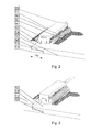
- the top planes 112, 122 of the boards may be coplanar as shown in the embodiment of Figs. 1-2 or parallel, but not coplanar, as shown in another embodiment of Fig. 3 .
- the boards 110, 120 comprise at least a pair of coaxial openings 113-123, 114-124.
- a connector 140 is mounted on the top plane 122 of the second PCB 120 by means of at least a pair of fastening elements 141, 142.
- the fastening elements 141, 142 extend through the coaxial openings 113-123, 114-124 and are fixed to the bottom plane 115 of the first PCB.
- the connector 140 comprises a plurality of contact members 143, which are electrically coupled with the circuit paths 111, 121.
- the PCB arrangement may further comprise a second connector 150, mounted on the bottom plane 115 of the first PCB 110 for connecting the circuit paths routed at the bottom planes 115, 125 and having fastening elements common with the first connector 140 and extending through the same coaxial openings 113-123, 114-124 in the first PCB 110 and in the second PCB 120.
- the connectors 140, 150 can be configured according to the embodiment shown in Fig. 7 and the fastening elements may be screws joining the openings in the connectors.
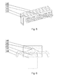
- the connector as shown in one embodiment in a perspective and cross-sectional view in Figs. 5-6 , has contact members 143 which have a first portion 144 for contacting the circuit path 111, 121 and a second portion 145 mechanically connected with the connector frame 146, wherein the first portion 144 is resiliently movable with respect to the second portion 145.
- the contact members 143 can be made of a resilient material, such as phosphor bronze or beryllium bronze.
- the contact members 143 and the circuit paths 111, 121 can be made of or coated by non-oxidizing metal, such as gold, which guarantees good conductivity while the PCB arrangement is in use.
- the resiliency of the contact members 143 compensates any irregularities of the assembly and guarantees constant contact of the members 143 and the circuit paths. Moreover, it allows to keep the contact even when the PCB arrangement is inclined or turned upside-down.
- the first portion 144 has a rounded edge so that contact with the circuit path is guaranteed. For more secure contact, the first portion 144 can be soldered to the circuit paths 111, 121.
- the connector may comprise a slotted main frame 146 to which the contact members 143 are mounted and a bottom part 147 which holds the contact members 143 in place.
- the fastening elements 141, 142 can be snap-type fasteners permanently fixed to the connector 140, for example to its main frame 146 as shown in Fig. 5 .
- the fastening elements can be separate from the connector 140, and the connector may comprise means for attaching the fastening elements, for example openings 148, 149 for screws.
- top plane and bottom plane as used throughout the description and claims are meant to clearly differentiate between two opposite planes of the PCB. It is evident that the actual orientation of these planes in the PCB arrangement will be defined by the orientation of the PCB arrangement as a whole or as mounted in an electronic device, and the PCB arrangement can be mounted with its top plane pointing upwards, downwards or inclined with respect to the horizontal line.
Landscapes
- Engineering & Computer Science (AREA)
- Microelectronics & Electronic Packaging (AREA)
- Coupling Device And Connection With Printed Circuit (AREA)
Abstract
Description
- The present invention relates to an arrangement of printed circuit boards (PCB) wherein two boards are interconnected.
- Modern electronic devices use electronic components of different complexity. On the one hand, sophisticated integrated circuit chips, such as signal processors operating at high frequencies with dozens or hundreds of input/output (I/O) lines are used, which require complicated routing of circuit paths. Such sophisticated chips have to be mounted on multi-layer PCBs, which are expensive and complicated to manufacture. On the other hand, simple devices such as power supply modules or low-speed input/output connectors are used, which require only a few signal path connections and can be mounted on single- or double-layer PCBs. So far, all devices have been usually mounted on a common circuit board. Such approach is not efficient, as the use of a multi-layer PCB for simple devices is not necessary.
- There are known PCB arrangements in which two PCBs are coupled together. For example, a US patent application
US20100134995A1 presents an electrical interconnection system comprising a pair of printed wiring boards have surfaces operable to be placed adjacent to one another such that an electrical circuit coupled to one printed wiring board is electrically coupled to another electrical circuit of the other printed wiring board by contact of the surface pads of each printing wiring board with one another. Such boards are relatively hard to manufacture and use dedicated, non-standard pads on the board. - The aim of the present invention is to provide an alternative PCB arrangement for interconnecting two boards, which allows manufacturing the PCBs in a standard technology.
- The object of the invention is a printed circuit board (PCB) arrangement, comprising a first PCB with circuit paths on a top plane, a second PCB with circuit paths on a top plane, partially overlapping the first PCB in an overlap area, wherein each of the first PCB and the second PCB comprises at least one opening situated within the overlap area such that the openings define a passage from the top plane of the second PCB to the bottom plane of the first PCB, wherein a connector is mounted on the top plane of the second PCB by means of at least one fastening element extending through the passage defined by the openings and fixed to the bottom plane of the first PCB, the connector comprising a plurality of contact members electrically coupled with the circuit paths of the top planes of the first PCB and the second PCB.
- Preferably, the first PCB comprises a plurality of openings, which are coaxial with corresponding openings of the second PCB and the connector comprises a plurality of fastening elements extending through the passages defined by the openings.
- Preferably, within the overlap area the first PCB and the second PCB have complementary stepped edges.
- Preferably, the top plane of the first PCB is coplanar with the top plane of the second PCB.
- Preferably, the top planes of the first PCB and of the second PCB are parallel and not coplanar.
- Preferably, the contact members of the connector have a first portion for contacting the circuit path and a second portion mechanically connected with the connector frame, wherein the first portion is resiliently movable with respect to the second portion.
- Preferably, the contact members are made of resilient material.
- Preferably, the fastening elements are snap-type fasteners permanently fixed to the connector.
- Preferably, the connector comprises means for attaching of fastening elements separate from the connector.
- Preferably, the contact members and the circuit paths are made of or coated by non-oxidising metal.
- Preferably, the PCB arrangement further comprises a connector mounted on the bottom plane of the first PCB by means of the pair of the fastening elements of the connector mounted on the top plane of the second PCB.
- The object of the invention is also an electronic device comprising the PCB arrangement according to the invention.
- The PCB arrangement according to the invention allows precise positioning of the PCBs, the connector and the circuit paths, by providing coaxial openings in the edge area of the PCBs, through which the fasteners coupled to the connector pass. This automatically positions all elements of the arrangement precisely with respect to each other. By providing resilient contact members, the arrangement is prone to vibrations and tolerant to dimensional imprecision of the PCBs. Due to contact-only connection, the connector can be easily decoupled and coupled to the PCB, without the need for soldering or other coupling, which allows easy mounting of the arrangement at the assembly stage and easy disassembly e.g. for servicing purposes. One of the PCBs may comprise electronic elements requiring complicated, multi-layer circuit paths or electronic elements operating with a high frequency, while the other PCB may comprise electronic elements requiring simple, single- or double-layer circuit paths or electronic elements operating with a low frequency.
- The object of the invention is shown by means of an exemplary embodiments on a drawing, in which:
-
Figs. 1-2 show an exploded and assembled view of one embodiment of the PCB arrangement, -
Fig. 3 shows an assembled view of another embodiment of the PCB arrangement, -
Fig. 4 shows an assembled view of yet another embodiment of the PCB arrangement, -
Figs. 5-6 show one embodiment of the connector in a perspective and cross-sectional view, -
Fig. 7 shows another embodiment of the connector in an exploded view, - The PCB arrangement according to the invention, shown in an exemplary embodiment in an exploded and assembled views on
Figs. 1-2 , comprises a first printed circuit board (PCB) 110 and asecond PCB 120 which are arranged in a partially overlapping manner. ThePCBs circuit paths top planes circuit paths boards other board boards overlap area 130. Within theoverlap area 130, thefirst board 110 and thesecond board 120 have complementarystepped edges overlap area 130 may be also shaped in a different manner, for example they can be chamfered. In the simplest embodiment, the edges may be straight and theboards top surfaces bottom surfaces top planes Figs. 1-2 or parallel, but not coplanar, as shown in another embodiment ofFig. 3 . Within theoverlap area 130, theboards connector 140 is mounted on thetop plane 122 of thesecond PCB 120 by means of at least a pair offastening elements fastening elements bottom plane 115 of the first PCB. Furthermore, theconnector 140 comprises a plurality ofcontact members 143, which are electrically coupled with thecircuit paths - The PCB arrangement, as shown in yet another embodiment on
Fig. 4 , may further comprise asecond connector 150, mounted on thebottom plane 115 of thefirst PCB 110 for connecting the circuit paths routed at thebottom planes first connector 140 and extending through the same coaxial openings 113-123, 114-124 in thefirst PCB 110 and in thesecond PCB 120. In that case, theconnectors Fig. 7 and the fastening elements may be screws joining the openings in the connectors. - The connector, as shown in one embodiment in a perspective and cross-sectional view in
Figs. 5-6 , hascontact members 143 which have afirst portion 144 for contacting thecircuit path connector frame 146, wherein thefirst portion 144 is resiliently movable with respect to the second portion 145. Thecontact members 143 can be made of a resilient material, such as phosphor bronze or beryllium bronze. Thecontact members 143 and thecircuit paths contact members 143 compensates any irregularities of the assembly and guarantees constant contact of themembers 143 and the circuit paths. Moreover, it allows to keep the contact even when the PCB arrangement is inclined or turned upside-down. Thefirst portion 144 has a rounded edge so that contact with the circuit path is guaranteed. For more secure contact, thefirst portion 144 can be soldered to thecircuit paths - The connector may comprise a slotted
main frame 146 to which thecontact members 143 are mounted and abottom part 147 which holds thecontact members 143 in place. - The
fastening elements connector 140, for example to itsmain frame 146 as shown inFig. 5 . In another embodiment, as shown inFig. 7 , the fastening elements can be separate from theconnector 140, and the connector may comprise means for attaching the fastening elements, forexample openings - The terms "top plane" and "bottom plane" as used throughout the description and claims are meant to clearly differentiate between two opposite planes of the PCB. It is evident that the actual orientation of these planes in the PCB arrangement will be defined by the orientation of the PCB arrangement as a whole or as mounted in an electronic device, and the PCB arrangement can be mounted with its top plane pointing upwards, downwards or inclined with respect to the horizontal line.
Claims (12)
- A printed circuit board (PCB) arrangement, comprising:- a first PCB (110) with circuit paths (111) on a top plane (112),- a second PCB (120) with circuit paths (121) on a top plane (122), partially overlapping the first PCB (110) in an overlap area (130),characterized in that- each of the first PCB (110) and the second PCB (120) comprises at least one opening (113-123, 114-124) situated within the overlap area (130) such that the openings (113-123, 114-124) define a passage from the top plane (122) of the second PCB (120) to the bottom plane (115) of the first PCB (110),- wherein a connector (140) is mounted on the top plane (122) of the second PCB (120) by means of at least one fastening element (141, 142) extending through the passage defined by the openings (113-123, 114-124) and fixed to the bottom plane (115) of the first PCB, the connector (140) comprising a plurality of contact members (143) electrically coupled with the circuit paths (111, 121) of the top planes (112, 122) of the first PCB (110) and the second PCB (120).
- The PCB arrangement according to claim 1, wherein the first PCB (110) comprises a plurality of openings (113, 114), which are coaxial with corresponding openings (123, 124) of the second PCB (120) and the connector (140) comprises a plurality of fastening elements (141, 142) extending through the passages defined by the openings (113-123, 114-124).
- The PCB arrangement according to any of claims 1-2, wherein within the overlap area (130) the first PCB (110) and the second PCB (120) have complementary stepped edges (116, 126).
- The PCB arrangement according to any of previous claims, wherein the top plane (112) of the first PCB (110) is coplanar with the top plane (122) of the second PCB (120).
- The PCB arrangement according to any of claims 1-3, wherein the top planes (112, 122) of the first PCB (110) and of the second PCB (120) are parallel and not coplanar.
- The PCB arrangement according to any of previous claims, wherein the contact members (143) of the connector (140) have a first portion (144) for contacting the circuit path (111, 121) and a second portion (145) mechanically connected with the connector frame (146), wherein the first portion (144) is resiliently movable with respect to the second portion (145).
- The PCB arrangement according to any of previous claims, wherein the contact members (143) are made of resilient material.
- The PCB arrangement according to any of previous claims, wherein the fastening elements (141, 142) are snap-type fasteners permanently fixed to the connector (140).
- The PCB arrangement according to any of previous claims, wherein the connector comprises means (148, 149) for attaching of fastening elements separate from the connector (140).
- The PCB arrangement according to any of previous claims, wherein the contact members (143) and the circuit paths (111, 121) are made of or coated by non-oxidising metal.
- The PCB arrangement according to any of previous claims, further comprising a connector (150) mounted on the bottom plane (115) of the first PCB (110) by means of the pair of the fastening elements (141, 142) of the connector (140) mounted on the top plane (122) of the second PCB (120).
- An electronic device comprising the PCB arrangement according to any of previous claims.
Priority Applications (2)
| Application Number | Priority Date | Filing Date | Title |
|---|---|---|---|
| EP11176064.1A EP2555600B1 (en) | 2011-07-30 | 2011-07-30 | A PCB arrangement |
| PCT/EP2012/064880 WO2013017563A1 (en) | 2011-07-30 | 2012-07-30 | A pcb arrangement |
Applications Claiming Priority (1)
| Application Number | Priority Date | Filing Date | Title |
|---|---|---|---|
| EP11176064.1A EP2555600B1 (en) | 2011-07-30 | 2011-07-30 | A PCB arrangement |
Publications (2)
| Publication Number | Publication Date |
|---|---|
| EP2555600A1 true EP2555600A1 (en) | 2013-02-06 |
| EP2555600B1 EP2555600B1 (en) | 2018-05-23 |
Family
ID=44487120
Family Applications (1)
| Application Number | Title | Priority Date | Filing Date |
|---|---|---|---|
| EP11176064.1A Not-in-force EP2555600B1 (en) | 2011-07-30 | 2011-07-30 | A PCB arrangement |
Country Status (2)
| Country | Link |
|---|---|
| EP (1) | EP2555600B1 (en) |
| WO (1) | WO2013017563A1 (en) |
Cited By (1)
| Publication number | Priority date | Publication date | Assignee | Title |
|---|---|---|---|---|
| EP4020717A1 (en) * | 2020-12-24 | 2022-06-29 | Intel Corporation | Ultra slim module form factor and connector architecture for inline connection |
Families Citing this family (1)
| Publication number | Priority date | Publication date | Assignee | Title |
|---|---|---|---|---|
| US12095189B2 (en) * | 2020-12-24 | 2024-09-17 | Intel Corporation | Ultra slim module form factor and connector architecture for top mount connection |
Citations (5)
| Publication number | Priority date | Publication date | Assignee | Title |
|---|---|---|---|---|
| GB2251128A (en) * | 1990-12-20 | 1992-06-24 | Tanashin Denki Co | A P.C.B mounting device |
| US5263868A (en) * | 1993-03-08 | 1993-11-23 | The Whitaker Corporation | Flexible circuit interface for coplanar printed circuit boards |
| JPH07321152A (en) * | 1994-03-29 | 1995-12-08 | Citizen Watch Co Ltd | Semiconductor device and manufacture thereof |
| DE102007039618A1 (en) * | 2007-08-22 | 2009-02-26 | Continental Automotive Gmbh | Module for integrated control electronics with simplified design |
| US20100134995A1 (en) | 2008-12-02 | 2010-06-03 | Raytheon Company | Electrical Interconnection System |
Family Cites Families (1)
| Publication number | Priority date | Publication date | Assignee | Title |
|---|---|---|---|---|
| US6109927A (en) * | 1998-08-27 | 2000-08-29 | The Whitaker Corporation | Connector for adjacent circuit-bearing substrates |
-
2011
- 2011-07-30 EP EP11176064.1A patent/EP2555600B1/en not_active Not-in-force
-
2012
- 2012-07-30 WO PCT/EP2012/064880 patent/WO2013017563A1/en not_active Ceased
Patent Citations (5)
| Publication number | Priority date | Publication date | Assignee | Title |
|---|---|---|---|---|
| GB2251128A (en) * | 1990-12-20 | 1992-06-24 | Tanashin Denki Co | A P.C.B mounting device |
| US5263868A (en) * | 1993-03-08 | 1993-11-23 | The Whitaker Corporation | Flexible circuit interface for coplanar printed circuit boards |
| JPH07321152A (en) * | 1994-03-29 | 1995-12-08 | Citizen Watch Co Ltd | Semiconductor device and manufacture thereof |
| DE102007039618A1 (en) * | 2007-08-22 | 2009-02-26 | Continental Automotive Gmbh | Module for integrated control electronics with simplified design |
| US20100134995A1 (en) | 2008-12-02 | 2010-06-03 | Raytheon Company | Electrical Interconnection System |
Cited By (2)
| Publication number | Priority date | Publication date | Assignee | Title |
|---|---|---|---|---|
| EP4020717A1 (en) * | 2020-12-24 | 2022-06-29 | Intel Corporation | Ultra slim module form factor and connector architecture for inline connection |
| US12184001B2 (en) | 2020-12-24 | 2024-12-31 | Intel Corporation | Ultra slim module form factor and connector architecture for inline connection |
Also Published As
| Publication number | Publication date |
|---|---|
| WO2013017563A1 (en) | 2013-02-07 |
| EP2555600B1 (en) | 2018-05-23 |
Similar Documents
| Publication | Publication Date | Title |
|---|---|---|
| KR101052807B1 (en) | Fixture of Printed Board Unit and Printed Board Unit | |
| US8727808B2 (en) | Electrical connector assembly for interconnecting an electronic module and an electrical component | |
| US6246016B1 (en) | Edge-mountable integrated circuit package and method of attaching the same to a printed wiring board | |
| JP5659440B2 (en) | Printed circuit board structure | |
| US10932378B2 (en) | Connector having pins extending to more than one printed circuit board | |
| CN101516162A (en) | Method and device for connecting circuit boards | |
| US20190006777A1 (en) | Printed Circuit Board Solder Joints | |
| EP2555600B1 (en) | A PCB arrangement | |
| EP2635097B1 (en) | An electric and/or electronic circuit including a printed circuit board, a separate circuit board and a power connector | |
| KR20220016236A (en) | Board structure with a different power supply circuit board | |
| US9941567B2 (en) | Integrated PCB interconnect system | |
| JP6443265B2 (en) | Mounting board | |
| US10276954B2 (en) | Board-to-board connectors and mounting structure | |
| TWI578862B (en) | Circuit module with lateral surface-mound pads and the corresponding system of the circuit module | |
| JP2006260842A (en) | Terminal mounting structure and its terminal mounting method | |
| US12550259B2 (en) | Electrically coupling printed circuit boards using a snap-fit connector | |
| KR101402617B1 (en) | Hybrid pcb of soldering type | |
| JP6177427B2 (en) | Printed wiring board unit | |
| JP6378906B2 (en) | Electronic circuit module substrate, multi-sided substrate for electronic circuit module substrate, and method for manufacturing electronic circuit module substrate | |
| JP2016149445A (en) | Power supply wiring member and printed circuit board wiring structure employing the member | |
| JP2009094176A (en) | Printed wiring board connection structure | |
| KR20090017297A (en) | Circuit board assembly | |
| US8270179B2 (en) | Printed circuit board and method for mounting electronic components | |
| KR20070056513A (en) | PCB board with pad (PAD) arrangement | |
| JP2008112915A (en) | Circuit board connection structure |
Legal Events
| Date | Code | Title | Description |
|---|---|---|---|
| PUAI | Public reference made under article 153(3) epc to a published international application that has entered the european phase |
Free format text: ORIGINAL CODE: 0009012 |
|
| 17P | Request for examination filed |
Effective date: 20120620 |
|
| AK | Designated contracting states |
Kind code of ref document: A1 Designated state(s): AL AT BE BG CH CY CZ DE DK EE ES FI FR GB GR HR HU IE IS IT LI LT LU LV MC MK MT NL NO PL PT RO RS SE SI SK SM TR |
|
| AX | Request for extension of the european patent |
Extension state: BA ME |
|
| RIC1 | Information provided on ipc code assigned before grant |
Ipc: H01R 12/70 20110101ALI20180111BHEP Ipc: H05K 1/14 20060101AFI20180111BHEP Ipc: H01R 12/73 20110101ALI20180111BHEP |
|
| GRAP | Despatch of communication of intention to grant a patent |
Free format text: ORIGINAL CODE: EPIDOSNIGR1 |
|
| STAA | Information on the status of an ep patent application or granted ep patent |
Free format text: STATUS: GRANT OF PATENT IS INTENDED |
|
| INTG | Intention to grant announced |
Effective date: 20180306 |
|
| GRAS | Grant fee paid |
Free format text: ORIGINAL CODE: EPIDOSNIGR3 |
|
| GRAA | (expected) grant |
Free format text: ORIGINAL CODE: 0009210 |
|
| STAA | Information on the status of an ep patent application or granted ep patent |
Free format text: STATUS: THE PATENT HAS BEEN GRANTED |
|
| AK | Designated contracting states |
Kind code of ref document: B1 Designated state(s): AL AT BE BG CH CY CZ DE DK EE ES FI FR GB GR HR HU IE IS IT LI LT LU LV MC MK MT NL NO PL PT RO RS SE SI SK SM TR |
|
| REG | Reference to a national code |
Ref country code: GB Ref legal event code: FG4D |
|
| REG | Reference to a national code |
Ref country code: CH Ref legal event code: EP |
|
| REG | Reference to a national code |
Ref country code: IE Ref legal event code: FG4D |
|
| REG | Reference to a national code |
Ref country code: DE Ref legal event code: R096 Ref document number: 602011048528 Country of ref document: DE |
|
| REG | Reference to a national code |
Ref country code: AT Ref legal event code: REF Ref document number: 1002594 Country of ref document: AT Kind code of ref document: T Effective date: 20180615 |
|
| REG | Reference to a national code |
Ref country code: FR Ref legal event code: PLFP Year of fee payment: 8 |
|
| REG | Reference to a national code |
Ref country code: NL Ref legal event code: MP Effective date: 20180523 |
|
| REG | Reference to a national code |
Ref country code: LT Ref legal event code: MG4D |
|
| PG25 | Lapsed in a contracting state [announced via postgrant information from national office to epo] |
Ref country code: ES Free format text: LAPSE BECAUSE OF FAILURE TO SUBMIT A TRANSLATION OF THE DESCRIPTION OR TO PAY THE FEE WITHIN THE PRESCRIBED TIME-LIMIT Effective date: 20180523 Ref country code: LT Free format text: LAPSE BECAUSE OF FAILURE TO SUBMIT A TRANSLATION OF THE DESCRIPTION OR TO PAY THE FEE WITHIN THE PRESCRIBED TIME-LIMIT Effective date: 20180523 Ref country code: NO Free format text: LAPSE BECAUSE OF FAILURE TO SUBMIT A TRANSLATION OF THE DESCRIPTION OR TO PAY THE FEE WITHIN THE PRESCRIBED TIME-LIMIT Effective date: 20180823 Ref country code: FI Free format text: LAPSE BECAUSE OF FAILURE TO SUBMIT A TRANSLATION OF THE DESCRIPTION OR TO PAY THE FEE WITHIN THE PRESCRIBED TIME-LIMIT Effective date: 20180523 Ref country code: BG Free format text: LAPSE BECAUSE OF FAILURE TO SUBMIT A TRANSLATION OF THE DESCRIPTION OR TO PAY THE FEE WITHIN THE PRESCRIBED TIME-LIMIT Effective date: 20180823 Ref country code: SE Free format text: LAPSE BECAUSE OF FAILURE TO SUBMIT A TRANSLATION OF THE DESCRIPTION OR TO PAY THE FEE WITHIN THE PRESCRIBED TIME-LIMIT Effective date: 20180523 |
|
| PG25 | Lapsed in a contracting state [announced via postgrant information from national office to epo] |
Ref country code: GR Free format text: LAPSE BECAUSE OF FAILURE TO SUBMIT A TRANSLATION OF THE DESCRIPTION OR TO PAY THE FEE WITHIN THE PRESCRIBED TIME-LIMIT Effective date: 20180824 Ref country code: RS Free format text: LAPSE BECAUSE OF FAILURE TO SUBMIT A TRANSLATION OF THE DESCRIPTION OR TO PAY THE FEE WITHIN THE PRESCRIBED TIME-LIMIT Effective date: 20180523 Ref country code: LV Free format text: LAPSE BECAUSE OF FAILURE TO SUBMIT A TRANSLATION OF THE DESCRIPTION OR TO PAY THE FEE WITHIN THE PRESCRIBED TIME-LIMIT Effective date: 20180523 Ref country code: HR Free format text: LAPSE BECAUSE OF FAILURE TO SUBMIT A TRANSLATION OF THE DESCRIPTION OR TO PAY THE FEE WITHIN THE PRESCRIBED TIME-LIMIT Effective date: 20180523 Ref country code: NL Free format text: LAPSE BECAUSE OF FAILURE TO SUBMIT A TRANSLATION OF THE DESCRIPTION OR TO PAY THE FEE WITHIN THE PRESCRIBED TIME-LIMIT Effective date: 20180523 |
|
| REG | Reference to a national code |
Ref country code: AT Ref legal event code: MK05 Ref document number: 1002594 Country of ref document: AT Kind code of ref document: T Effective date: 20180523 |
|
| PG25 | Lapsed in a contracting state [announced via postgrant information from national office to epo] |
Ref country code: CZ Free format text: LAPSE BECAUSE OF FAILURE TO SUBMIT A TRANSLATION OF THE DESCRIPTION OR TO PAY THE FEE WITHIN THE PRESCRIBED TIME-LIMIT Effective date: 20180523 Ref country code: RO Free format text: LAPSE BECAUSE OF FAILURE TO SUBMIT A TRANSLATION OF THE DESCRIPTION OR TO PAY THE FEE WITHIN THE PRESCRIBED TIME-LIMIT Effective date: 20180523 Ref country code: SK Free format text: LAPSE BECAUSE OF FAILURE TO SUBMIT A TRANSLATION OF THE DESCRIPTION OR TO PAY THE FEE WITHIN THE PRESCRIBED TIME-LIMIT Effective date: 20180523 Ref country code: DK Free format text: LAPSE BECAUSE OF FAILURE TO SUBMIT A TRANSLATION OF THE DESCRIPTION OR TO PAY THE FEE WITHIN THE PRESCRIBED TIME-LIMIT Effective date: 20180523 Ref country code: PL Free format text: LAPSE BECAUSE OF FAILURE TO SUBMIT A TRANSLATION OF THE DESCRIPTION OR TO PAY THE FEE WITHIN THE PRESCRIBED TIME-LIMIT Effective date: 20180523 Ref country code: AT Free format text: LAPSE BECAUSE OF FAILURE TO SUBMIT A TRANSLATION OF THE DESCRIPTION OR TO PAY THE FEE WITHIN THE PRESCRIBED TIME-LIMIT Effective date: 20180523 Ref country code: EE Free format text: LAPSE BECAUSE OF FAILURE TO SUBMIT A TRANSLATION OF THE DESCRIPTION OR TO PAY THE FEE WITHIN THE PRESCRIBED TIME-LIMIT Effective date: 20180523 |
|
| REG | Reference to a national code |
Ref country code: DE Ref legal event code: R097 Ref document number: 602011048528 Country of ref document: DE |
|
| PG25 | Lapsed in a contracting state [announced via postgrant information from national office to epo] |
Ref country code: SM Free format text: LAPSE BECAUSE OF FAILURE TO SUBMIT A TRANSLATION OF THE DESCRIPTION OR TO PAY THE FEE WITHIN THE PRESCRIBED TIME-LIMIT Effective date: 20180523 Ref country code: IT Free format text: LAPSE BECAUSE OF FAILURE TO SUBMIT A TRANSLATION OF THE DESCRIPTION OR TO PAY THE FEE WITHIN THE PRESCRIBED TIME-LIMIT Effective date: 20180523 |
|
| REG | Reference to a national code |
Ref country code: CH Ref legal event code: PL |
|
| PG25 | Lapsed in a contracting state [announced via postgrant information from national office to epo] |
Ref country code: MC Free format text: LAPSE BECAUSE OF FAILURE TO SUBMIT A TRANSLATION OF THE DESCRIPTION OR TO PAY THE FEE WITHIN THE PRESCRIBED TIME-LIMIT Effective date: 20180523 Ref country code: LU Free format text: LAPSE BECAUSE OF NON-PAYMENT OF DUE FEES Effective date: 20180730 |
|
| PLBE | No opposition filed within time limit |
Free format text: ORIGINAL CODE: 0009261 |
|
| STAA | Information on the status of an ep patent application or granted ep patent |
Free format text: STATUS: NO OPPOSITION FILED WITHIN TIME LIMIT |
|
| REG | Reference to a national code |
Ref country code: BE Ref legal event code: MM Effective date: 20180731 |
|
| PG25 | Lapsed in a contracting state [announced via postgrant information from national office to epo] |
Ref country code: LI Free format text: LAPSE BECAUSE OF NON-PAYMENT OF DUE FEES Effective date: 20180731 Ref country code: CH Free format text: LAPSE BECAUSE OF NON-PAYMENT OF DUE FEES Effective date: 20180731 |
|
| 26N | No opposition filed |
Effective date: 20190226 |
|
| REG | Reference to a national code |
Ref country code: IE Ref legal event code: MM4A |
|
| PG25 | Lapsed in a contracting state [announced via postgrant information from national office to epo] |
Ref country code: BE Free format text: LAPSE BECAUSE OF NON-PAYMENT OF DUE FEES Effective date: 20180731 Ref country code: SI Free format text: LAPSE BECAUSE OF FAILURE TO SUBMIT A TRANSLATION OF THE DESCRIPTION OR TO PAY THE FEE WITHIN THE PRESCRIBED TIME-LIMIT Effective date: 20180523 |
|
| PG25 | Lapsed in a contracting state [announced via postgrant information from national office to epo] |
Ref country code: IE Free format text: LAPSE BECAUSE OF NON-PAYMENT OF DUE FEES Effective date: 20180730 |
|
| PG25 | Lapsed in a contracting state [announced via postgrant information from national office to epo] |
Ref country code: AL Free format text: LAPSE BECAUSE OF FAILURE TO SUBMIT A TRANSLATION OF THE DESCRIPTION OR TO PAY THE FEE WITHIN THE PRESCRIBED TIME-LIMIT Effective date: 20180523 |
|
| PG25 | Lapsed in a contracting state [announced via postgrant information from national office to epo] |
Ref country code: MT Free format text: LAPSE BECAUSE OF NON-PAYMENT OF DUE FEES Effective date: 20180730 |
|
| PG25 | Lapsed in a contracting state [announced via postgrant information from national office to epo] |
Ref country code: TR Free format text: LAPSE BECAUSE OF FAILURE TO SUBMIT A TRANSLATION OF THE DESCRIPTION OR TO PAY THE FEE WITHIN THE PRESCRIBED TIME-LIMIT Effective date: 20180523 |
|
| PG25 | Lapsed in a contracting state [announced via postgrant information from national office to epo] |
Ref country code: PT Free format text: LAPSE BECAUSE OF FAILURE TO SUBMIT A TRANSLATION OF THE DESCRIPTION OR TO PAY THE FEE WITHIN THE PRESCRIBED TIME-LIMIT Effective date: 20180523 Ref country code: HU Free format text: LAPSE BECAUSE OF FAILURE TO SUBMIT A TRANSLATION OF THE DESCRIPTION OR TO PAY THE FEE WITHIN THE PRESCRIBED TIME-LIMIT; INVALID AB INITIO Effective date: 20110730 |
|
| PG25 | Lapsed in a contracting state [announced via postgrant information from national office to epo] |
Ref country code: CY Free format text: LAPSE BECAUSE OF FAILURE TO SUBMIT A TRANSLATION OF THE DESCRIPTION OR TO PAY THE FEE WITHIN THE PRESCRIBED TIME-LIMIT Effective date: 20180523 Ref country code: MK Free format text: LAPSE BECAUSE OF NON-PAYMENT OF DUE FEES Effective date: 20180523 |
|
| PG25 | Lapsed in a contracting state [announced via postgrant information from national office to epo] |
Ref country code: IS Free format text: LAPSE BECAUSE OF FAILURE TO SUBMIT A TRANSLATION OF THE DESCRIPTION OR TO PAY THE FEE WITHIN THE PRESCRIBED TIME-LIMIT Effective date: 20180923 |
|
| PGFP | Annual fee paid to national office [announced via postgrant information from national office to epo] |
Ref country code: GB Payment date: 20230727 Year of fee payment: 13 |
|
| PGFP | Annual fee paid to national office [announced via postgrant information from national office to epo] |
Ref country code: FR Payment date: 20230725 Year of fee payment: 13 Ref country code: DE Payment date: 20230727 Year of fee payment: 13 |
|
| REG | Reference to a national code |
Ref country code: DE Ref legal event code: R119 Ref document number: 602011048528 Country of ref document: DE |
|
| GBPC | Gb: european patent ceased through non-payment of renewal fee |
Effective date: 20240730 |
|
| PG25 | Lapsed in a contracting state [announced via postgrant information from national office to epo] |
Ref country code: DE Free format text: LAPSE BECAUSE OF NON-PAYMENT OF DUE FEES Effective date: 20250201 |
|
| PG25 | Lapsed in a contracting state [announced via postgrant information from national office to epo] |
Ref country code: FR Free format text: LAPSE BECAUSE OF NON-PAYMENT OF DUE FEES Effective date: 20240731 |
|
| PG25 | Lapsed in a contracting state [announced via postgrant information from national office to epo] |
Ref country code: GB Free format text: LAPSE BECAUSE OF NON-PAYMENT OF DUE FEES Effective date: 20240730 |