EP2555494A1 - Antenna device and communication device - Google Patents
Antenna device and communication device Download PDFInfo
- Publication number
- EP2555494A1 EP2555494A1 EP11765750A EP11765750A EP2555494A1 EP 2555494 A1 EP2555494 A1 EP 2555494A1 EP 11765750 A EP11765750 A EP 11765750A EP 11765750 A EP11765750 A EP 11765750A EP 2555494 A1 EP2555494 A1 EP 2555494A1
- Authority
- EP
- European Patent Office
- Prior art keywords
- antenna
- antenna coil
- magnetic sheet
- communication device
- transmitter
- Prior art date
- Legal status (The legal status is an assumption and is not a legal conclusion. Google has not performed a legal analysis and makes no representation as to the accuracy of the status listed.)
- Granted
Links
Images














Classifications
-
- H—ELECTRICITY
- H01—ELECTRIC ELEMENTS
- H01Q—ANTENNAS, i.e. RADIO AERIALS
- H01Q1/00—Details of, or arrangements associated with, antennas
- H01Q1/12—Supports; Mounting means
- H01Q1/22—Supports; Mounting means by structural association with other equipment or articles
- H01Q1/24—Supports; Mounting means by structural association with other equipment or articles with receiving set
- H01Q1/241—Supports; Mounting means by structural association with other equipment or articles with receiving set used in mobile communications, e.g. GSM
- H01Q1/242—Supports; Mounting means by structural association with other equipment or articles with receiving set used in mobile communications, e.g. GSM specially adapted for hand-held use
- H01Q1/243—Supports; Mounting means by structural association with other equipment or articles with receiving set used in mobile communications, e.g. GSM specially adapted for hand-held use with built-in antennas
-
- H—ELECTRICITY
- H01—ELECTRIC ELEMENTS
- H01Q—ANTENNAS, i.e. RADIO AERIALS
- H01Q1/00—Details of, or arrangements associated with, antennas
- H01Q1/12—Supports; Mounting means
- H01Q1/22—Supports; Mounting means by structural association with other equipment or articles
- H01Q1/2208—Supports; Mounting means by structural association with other equipment or articles associated with components used in interrogation type services, i.e. in systems for information exchange between an interrogator/reader and a tag/transponder, e.g. in Radio Frequency Identification [RFID] systems
-
- G—PHYSICS
- G06—COMPUTING OR CALCULATING; COUNTING
- G06K—GRAPHICAL DATA READING; PRESENTATION OF DATA; RECORD CARRIERS; HANDLING RECORD CARRIERS
- G06K19/00—Record carriers for use with machines and with at least a part designed to carry digital markings
- G06K19/06—Record carriers for use with machines and with at least a part designed to carry digital markings characterised by the kind of the digital marking, e.g. shape, nature, code
- G06K19/067—Record carriers with conductive marks, printed circuits or semiconductor circuit elements, e.g. credit or identity cards also with resonating or responding marks without active components
- G06K19/07—Record carriers with conductive marks, printed circuits or semiconductor circuit elements, e.g. credit or identity cards also with resonating or responding marks without active components with integrated circuit chips
- G06K19/077—Constructional details, e.g. mounting of circuits in the carrier
-
- H—ELECTRICITY
- H01—ELECTRIC ELEMENTS
- H01Q—ANTENNAS, i.e. RADIO AERIALS
- H01Q1/00—Details of, or arrangements associated with, antennas
- H01Q1/12—Supports; Mounting means
- H01Q1/22—Supports; Mounting means by structural association with other equipment or articles
- H01Q1/2208—Supports; Mounting means by structural association with other equipment or articles associated with components used in interrogation type services, i.e. in systems for information exchange between an interrogator/reader and a tag/transponder, e.g. in Radio Frequency Identification [RFID] systems
- H01Q1/2225—Supports; Mounting means by structural association with other equipment or articles associated with components used in interrogation type services, i.e. in systems for information exchange between an interrogator/reader and a tag/transponder, e.g. in Radio Frequency Identification [RFID] systems used in active tags, i.e. provided with its own power source or in passive tags, i.e. deriving power from RF signal
-
- H—ELECTRICITY
- H01—ELECTRIC ELEMENTS
- H01Q—ANTENNAS, i.e. RADIO AERIALS
- H01Q1/00—Details of, or arrangements associated with, antennas
- H01Q1/12—Supports; Mounting means
- H01Q1/22—Supports; Mounting means by structural association with other equipment or articles
- H01Q1/24—Supports; Mounting means by structural association with other equipment or articles with receiving set
-
- H—ELECTRICITY
- H01—ELECTRIC ELEMENTS
- H01Q—ANTENNAS, i.e. RADIO AERIALS
- H01Q1/00—Details of, or arrangements associated with, antennas
- H01Q1/42—Housings not intimately mechanically associated with radiating elements, e.g. radome
-
- H—ELECTRICITY
- H01—ELECTRIC ELEMENTS
- H01Q—ANTENNAS, i.e. RADIO AERIALS
- H01Q7/00—Loop antennas with a substantially uniform current distribution around the loop and having a directional radiation pattern in a plane perpendicular to the plane of the loop
-
- H—ELECTRICITY
- H01—ELECTRIC ELEMENTS
- H01Q—ANTENNAS, i.e. RADIO AERIALS
- H01Q7/00—Loop antennas with a substantially uniform current distribution around the loop and having a directional radiation pattern in a plane perpendicular to the plane of the loop
- H01Q7/06—Loop antennas with a substantially uniform current distribution around the loop and having a directional radiation pattern in a plane perpendicular to the plane of the loop with core of ferromagnetic material
-
- H—ELECTRICITY
- H01—ELECTRIC ELEMENTS
- H01Q—ANTENNAS, i.e. RADIO AERIALS
- H01Q1/00—Details of, or arrangements associated with, antennas
- H01Q1/12—Supports; Mounting means
- H01Q1/22—Supports; Mounting means by structural association with other equipment or articles
- H01Q1/2258—Supports; Mounting means by structural association with other equipment or articles used with computer equipment
- H01Q1/2266—Supports; Mounting means by structural association with other equipment or articles used with computer equipment disposed inside the computer
Definitions
- the reader/writer 120 functions as a transmitter that transmits a magnetic field in a z-axis direction to the communication device 1 facing the reader/writer 120 on the x-y plane. More specifically, the reader/writer 120 includes an antenna 121 that transmits a magnetic field to the communication device 1 and a control board 122 that communicates with the communication device 1 inductively coupled through the antenna 121.
- the communication device 5 when the conductive plate 54 is arranged between the circuit board 132 and the antenna substrate 51, in comparison with the case in which the conductive plate 54 is not arranged, the Q value is large and slightly changes. As is apparent from the result, the communication device 5 can be stably operated while maintaining preferable communication characteristics.
- the communication device 5 is especially preferably designed such that a circumference of the conductive plate 54 is equal to a circumference of the antenna coil 51a.
- a width W2 of the conductive plate 54 is set to be larger than a width W1 of the antenna coil 51a regulated in a y-axis direction to make it possible to realize more preferable communication characteristics.
- a communication device employs a structure in which an antenna coil and a magnetic sheet are superposed on each other to have almost the same plane on both the surfaces on a reader/writer side and a substrate side so as to realize a small thickness and preferable communication characteristics.
- a step portion 631 is formed on the magnetic sheet 63 at the center portion 61c.
Landscapes
- Engineering & Computer Science (AREA)
- Computer Networks & Wireless Communication (AREA)
- Computer Hardware Design (AREA)
- Microelectronics & Electronic Packaging (AREA)
- Physics & Mathematics (AREA)
- General Physics & Mathematics (AREA)
- Theoretical Computer Science (AREA)
- General Engineering & Computer Science (AREA)
- Telephone Set Structure (AREA)
- Near-Field Transmission Systems (AREA)
- Support Of Aerials (AREA)
- Details Of Aerials (AREA)
Abstract

Description
- This present invention relates to an antenna device and a communication device that are built in an electronic device and can perform communication by receiving a magnetic field transmitted from a transmitter.
- The present application asserts priority rights based on
JP Patent Application 2010-082037 JP Patent Application 2011-070666 - An electronic device such as a mobile phone uses an antenna module for RFID (Radio Frequency Identification) to mount a near field contactless communication function thereon.
- The antenna module performs communication with an antenna coil mounted on a transmitter such as a reader/writer by using inductive coupling. More specifically, in the antenna module, the antenna coil receives a magnetic field from the reader/writer to make it possible to drive an IC that converts the magnetic field into an electric power to function as a communication processing unit.
- The antenna module must receive a magnetic flux having a certain value or more from the reader/writer to reliably perform communication. For this purpose, in the antenna module according to the conventional technique, a loop coil is arranged in the housing of the mobile phone to receive a magnetic flux from the reader/writer with the coil.
- However, in an antenna module built in an electronic device such as a mobile phone, since magnetic fluxes from the reader/writer are reflected by an eddy current generated when a metal contained in a circuit board in the device or a buttery pack receives a magnetic field from the reader/writer, a smaller number of magnetic fluxes reach the loop coil. In this manner, since the number of magnetic fluxes reaching the loop coil becomes small, the antenna module requires a loop coil having a certain size to collect required magnetic fluxes. Furthermore, the number of magnetic fluxes must be increased by using a magnetic sheet.
- As described above, magnetic fluxes from a reader/writer are reflected by an eddy current flowing in a circuit board of an electronic device such as a mobile phone, some magnetic field components face an surface direction of the circuit board are present on a housing source of the electronic device. A coil that receive the components to function as an antenna is proposed in
Patent Document 1. More specifically, inPatent Document 1, in order to reduce an occupied area of a coil, an antenna structure obtained by winding a coil on a ferrite core is proposed. Citation List -
- Patent Document 1: Japanese Unexamined Patent Publication No.
2008-35464 - As described above, since an electronic device such as a mobile phone uses a circuit board or the like that is relatively conductive, an eddy current is generated in the circuit board that receives a magnetic field to reflect the magnetic field. For example, in consideration of the housing surface of a mobile phone, a magnetic field transmitted from a reader/writer tends to be strong at a peripheral portion of the housing surface and to be weak near the center of the housing surface.
- In an antenna using a normal loop coil, the loop coil has an opening located at a center portion of a mobile phone that cannot receive a large amount of magnetic field passing through the outer peripheral portion of the housing surface described above. For this reason, in an antenna using a normal loop coil, efficiency of receiving a magnetic field is deteriorated.
- In an antenna structure in which a coil is winded on a ferrite core described in
Patent Document 1 and the coil is built in a mobile phone, a section of the ferrite core has an area that collects magnetic fluxes. For this reason, the ferrite core requires a thickness of, for example, 1 mm or more, and the housing of the mobile phone has a relatively thick structure. Thus, in a relatively thin mobile phone, the structure is difficult to be mounted. When the antenna module is built on a rear side of a liquid-crystal display mounted on a foldable mobile phone, the antenna module is also required to be thin. For this reason, a space for the antenna structure described inPatent Document 1 cannot be easily secured. - The present invention has been proposed in consideration of the above circumstances, and has as its object to provide an antenna device and a communication device that can reduce a housing of an electronic device in size and thickness when the antenna device and the communication device are built in the electronic device while keeping communication characteristics.
- In order to solve the above problem, the present invention provides an antenna device that is built in an electronic device and that can perform communication by receiving a magnetic field transmitted from a transmitter, including: an antenna coil arranged on an outer peripheral portion of a housing surface facing the transmitter of the electronic device and inductively coupled to the transmitter; and a magnetic sheet that attracts a magnetic field transmitted from the transmitter to the antenna coil, wherein the antenna coil and the magnetic sheet are superposed on each other to satisfy at least one of arrangement conditions including an arrangement condition in which the magnetic sheet is located on the transmitter side of the antenna coil on a center side of the housing surface and an arrangement condition in which the antenna coil is located on the transmitter side of the magnetic sheet on an outer periphery side of the housing surface.
- The present invention provides a communication device that is built in an electronic device and can perform communication by receiving a magnetic field transmitted from a transmitter, including: an antenna coil arranged on an outer peripheral portion of a housing surface facing the transmitter of the electronic device and inductively coupled to the transmitter; a magnetic sheet that attracts a magnetic field transmitted from the transmitter to the antenna coil; and a communication processing unit that is driven by a current flowing in the antenna coil and performs communication with the transmitter, wherein the antenna coil and the magnetic sheet are superposed on each other to satisfy at least one of arrangement conditions including an arrangement condition in which the magnetic sheet is located on the transmitter side of the antenna coil on a center side of the housing surface and an arrangement condition in which the antenna coil is located on the transmitter side of the magnetic sheet on an outer periphery side of the housing surface.
- According to the present invention, the antenna coil and the magnetic sheet are superposed on each other to satisfy at least one of the arrangement conditions including the arrangement condition in which the magnetic sheet is located on the transmitter side of the antenna coil on the center side of the housing surface and the arrangement condition in which the antenna coil is located on the transmitter side of the magnetic sheet on the outer periphery side of the housing surface. When the magnetic sheet is arranged as described above, according to the present invention, magnetic fluxes generated on the outer peripheral portion of the housing surface of the electronic device facing the transmitter can be efficiently attracted to the antenna coil to make it possible to reduce the housing of the electronic device in size and thickness when the antenna device or the communication device is built in the electronic device by arranging the antenna coil is arranged on the outer peripheral portion while maintaining communication characteristics.
-
-
FIG. 1 is a diagram for explaining a configuration of a wireless communication system in which a communication device to which the present invention is applied is built. -
FIG. 2 is a diagram for explaining a configuration of a communication device arranged in a housing of a mobile phone. -
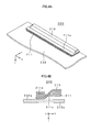
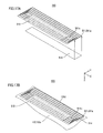
FIG. 3A is a perspective view of an antenna substrate according to a first example, andFIG. 3B is a sectional view of an antenna substrate according to the first example. -
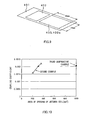
FIG. 4A is a perspective view of an antenna substrate according to a first comparative example, andFIG. 4B is a sectional view of the antenna substrate according to the first comparative example. -
FIG. 5 is a graph showing a measurement result related to communication characteristics between the communication device according to the first example and the communication device according to the first comparative example. -
FIG. 6A is a perspective view of an antenna substrate according to a second comparative example, andFIG. 6B is a sectional view of the antenna substrate according to the second comparative example. -
FIG. 7 is a graph showing a measurement result related to communication characteristics between the communication device according to the first example and the communication device according to the second comparative example. -
FIG. 8 is a perspective view of an antenna substrate in which the number of turns of an antenna coil is set to 8, a width W orthogonal to an outer periphery is set to 10 [mm], a length along the outer periphery is set to L [mm], and a magnetic sheet is inserted into a center portion of the antenna coil in the communication device according to a second example. -
FIG. 9 is a diagram for explaining a configuration of a communication device according to a third comparative example. -
FIG. 10 is a graph for explaining changes of communication characteristics when an area of the antenna coil is changed by changing a value of a length L of one side of the antenna coil. -
FIG. 11A is a perspective view of an antenna substrate according to a third example, andFIG. 11B is a sectional view of the antenna substrate according to the third example. -
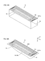
FIG. 12A is a perspective view of an antenna substrate according to a fourth example, andFIG. 12B is a sectional view according to the antenna substrate according to the fourth example. -
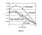
FIG. 13 is a graph for explaining communication characteristics of a reader/writer and communication devices when distances between the reader/writer and a mobile telephone is changed. -
FIG. 14A is a diagram showing a configuration of a configuration of a conductive plate superposed on an antenna substrate according to a fifth example, andFIG. 14B is a perspective view showing the antenna substrate according to the fifth example. -
FIG. 15A is a graph for explaining characteristics of a resistance of the antenna coil according to the fifth example,FIG. 15B is a graph for explaining characteristics of an inductance of the antenna coil according to the fifth example. -
FIG. 16 is a graph for explaining characteristics of a Q value of the antenna coil according to the fifth example. -
FIG. 17A is a diagram showing a configuration of a conductive plate superposed on an antenna substrate according to a fourth comparative example, andFIG. 17B is a perspective view showing the antenna substrate according to the fourth comparative example. -
FIG. 18A is a diagram showing a configuration of a conductive plate superposed on an antenna substrate according a fifth comparative example, andFIG. 18B is a perspective view showing the antenna substrate according to the fifth comparative example. -
FIG. 19A is a graph for explaining characteristics of a resistance of an antenna coil according to the fifth example, andFIG. 19B is a graph for explaining characteristics of an inductance of the antenna coil according to the fifth example. -
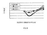
FIG. 20 is a graph for explaining characteristics of a Q value of the antenna coil according to the fifth example. -
FIG. 21 is a diagram for explaining a change of communication characteristics of the antenna coil according to the fifth example depending on a change of the shape of the conductive plate. -
FIG. 22A is a graph showing a Q value of the antenna coil according to the fifth example depending on the change of the shape of the conductive plate, andFIG. 22B is a graph showing a coupling coefficient of the antenna coil according to the fifth example depending on the change of the shape of the conductive plate. -
FIG. 23 is a diagram for explaining a concrete arrangement of the antenna substrate according to a fifth embodiment. -
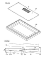
FIG. 24A is a diagram for explaining a configuration of the antenna substrate according to the fifth embodiment mounted on a surface of a storing lid, andFIG. 24B is a diagram for explaining a configuration of a terminal portion formed on the antenna substrate according to the fifth embodiment. -
FIG. 25A is a diagram showing a positional relationship between a communication device according to a sixth example and a reader/writer, andFIG. 25B is a sectional view of an antenna substrate according to the communication device according to the sixth example. -
FIG. 26 is a diagram showing a communication device having a structure in which an antenna coil is inserted between magnetic sheets each having both horizontal surfaces such that a step portion is formed on a center portion of the antenna substrate. -
FIG. 27A is a graph showing a coupling coefficient of the communication device according to the sixth example when the magnetic sheet is change in thickness while keeping the thickness of the antenna substrate constant, andFIG. 27B is a graph showing a coupling coefficient of the communication device according to the sixth example when the antenna substrate is changed in thickness while keeping the thickness of the magnetic sheet constant. -
FIG. 28 is a graph showing a coupling coefficient obtained when a conductive line of the antenna coil according to the sixth example is changed in thickness in concrete examples of three types in which total thicknesses of antenna substrates and magnetic sheets are set to 0.3 mm, 0.4 mm, and 0.5 mm. -
FIG. 29 is a graph showing Q values obtained when a conductive line of the antenna coil according to the sixth example is changed in thickness in concrete examples of three types in which total thicknesses of antenna substrates and magnetic sheets are set to 0.3 mm, 0.4 mm, and 0.5 mm. -
FIG. 30 is a graph showing products of coupling coefficients and Q values obtained when a conductive line of the antenna coil according to the sixth example is changed in thickness in concrete examples of three types in which total thicknesses of antenna substrates and magnetic sheets are set to 0.3 mm, 0.4 mm, and 0.5 mm. -
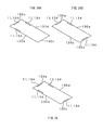
FIG. 31A is a diagram showing an antenna substrate arranged on an outer peripheral portion on anouter periphery 130d side,FIG. 31B is a diagram showing an antenna substrate arranged on an outer peripheral portion on anotherouter periphery 130b side,FIG. 31C is a diagram showing an antenna substrate arranged on an outer peripheral portion on still another outer periphery 130a side, andFIG. 31D is a diagram showing an antenna substrate arranged on an outer peripheral portion on still anotherouter periphery 130c side. -
FIG. 32 is a graph for explaining a change in communication sensitivity when relative positions of a mobile phone in which a communication device is built and a reader/writer are changed. -
FIG. 33A is a diagram showing two antenna substrates arranged on outer peripheral portions on theouter periphery 130b side and theouter periphery 130d side, andFIG. 33B is a diagram showing two antenna substrates arranged on outer peripheral portions on the outer periphery 130a side and theouter periphery 130c side. -
FIG. 34A is a diagram showing three antenna substrates arranged on the outer peripheral portions of the outer periphery 130a side, theouter periphery 130b side, and theouter periphery 130d side, andFIG. 34B is a diagram showing two antenna substrates arranged on the outer peripheral portions of the outer periphery 130a side, theouter periphery 130c side, and theouter periphery 130d side. -
FIG. 35 is a diagram showing four antenna substrates arranged on the outer peripheral portions of the outer periphery 130a side, theouter periphery 130b side, theouter periphery 130c side, and theouter periphery 130d side. - Embodiments to execute the present invention will be described in detail with reference to the accompanying drawings. The present invention is not limited to only the embodiments, and various changes of the present invention can be effected without departing from the spirit and scope of the invention, as a matter of course.
- A communication device to which the present invention is applied is a device that is built in an electronic device and that can perform communication by receiving a magnetic field transmitted from a transmitter.
The communication device is used by being built in awireless communication system 100 for RFID (Radio Frequency Identification) as shown in, for example,FIG. 1 . - The
wireless communication system 100 includes acommunication device 1 according to a first example to which the present invention is applied and a reader/writer 120 that accesses thecommunication device 1. In this case, it is assumed that thecommunication device 1 and the reader/writer 120 are arranged to face each other on an x-y plane of a three-dimensional orthogonal coordinate system xyz. - The reader/
writer 120 functions as a transmitter that transmits a magnetic field in a z-axis direction to thecommunication device 1 facing the reader/writer 120 on the x-y plane. More specifically, the reader/writer 120 includes anantenna 121 that transmits a magnetic field to thecommunication device 1 and acontrol board 122 that communicates with thecommunication device 1 inductively coupled through theantenna 121. - More specifically, in the reader/
writer 120, thecontrol board 122 electrically connected to theantenna 121 is arranged. A control circuit including electronic parts such as one or a plurality of integrated circuit chips is mounted on thecontrol board 122. The control circuit executes processes of various types on the basis of data received from thecommunication device 1. For example, when the control circuit transmits data to thecommunication device 1, the control circuit encodes the data, modulates a carrier wave having a predetermined frequency (for example, 13.56 MHz) on the basis of the encoded data, amplifies the modulated modulating signal, and causes the modulating signal to drive theantenna 121.
When the control circuit reads data from thecommunication device 1, the control circuit amplifies a modulating signal of the data received by theantenna 121, demodulates the amplified modulating signal of the data, and decodes the demodulated data. In the control circuit, an encoding method and a modulating method used in a general reader/writer are used. For example, the Manchester encoding method or the ASK (Amplitude Shift Keying) modulating method is used. - The
communication device 1 is built in a housing 131 of amobile phone 130 arranged to face the reader/writer 120 on the x-y plane, and includes anantenna substrate 11 on which an antenna coil 11a that can communicate with the inductively coupled reader/writer 120 is mounted, and acommunication processing unit 12 that is driven by a current flowing in the antenna coil 11a to communicate with the reader/writer 120. - On the
antenna substrate 11, the antenna coil 11a formed by performing a patterning process or the like to a flexible conductor such as a flexible flat cable and aterminal unit 11b electrically connected to the antenna coil 11a and thecommunication processing unit 12. - When the antenna coil 11a receives a magnetic field generated from the reader/
writer 120, the antenna coil 11a magnetically coupled to the reader/writer 120 by inductive coupling, receives a modulated carrier wave, and supplies the received signal to thecommunication processing unit 12 through theterminal unit 11b. - The
communication processing unit 12 is driven by a current flowing in the antenna coil 11a and communicates with the reader/writer 120. More specifically, thecommunication processing unit 12 demodulates the received modulating signal, decodes the demodulated data, and writes the decoded data in an internal memory included in thecommunication processing unit 12.
Thecommunication processing unit 12 reads data transmitted to the reader/writer 120 from the internal memory, encodes the read data, modulates a carrier wave on the basis of the encoded data, and transmits the modulated radio wave to the reader/writer 120 through theantenna substrate 11 magnetically coupled by inductive coupling. - <First Embodiment>
- In the
wireless communication system 100 having the above configuration, the configuration of thecommunication device 1 according to the first example will be described below as the first embodiment. - The
communication device 1 according to the first example, in terms of realization of reductions in size and thickness of an electronic device such as themobile phone 130 when thecommunication device 1 is built in the electronic device while maintaining communication characteristics between the reader/writer 120 and thecommunication device 1, for example, is arranged on acircuit board 132 in the housing 131 of themobile phone 130 on a Z-y plane of the three-dimensional orthogonal coordinate system xyz. InFIG. 2 , it is assumed that amagnetic sheet 133 to cover a battery pack to drive themobile phone 130 is arranged in a partial region of thecircuit board 132 in the housing 131 of themobile phone 130 - The antenna coil 11a of the
communication device 1 is preferably arranged at a position where a magnetic field from the reader/writer 120 is strong to maintain the communication characteristics between the antenna coil 11a and the reader/writer 120. In this case, since thecircuit board 132 of themobile phone 130 easily conducts electricity, an eddy current is generated when an external AC magnetic field is applied to thecircuit board 132 to reflect a magnetic field. When a magnetic field distribution obtained by applying an external AC is examined, magnetic fields of the fourperipheries mobile phone 130 arranged to face the reader/writer 120 are strong. - In this case, by using the characteristics of magnetic field strength in the housing 131 of the
mobile phone 130, thecommunication device 1, as shown inFIG. 2 , is arranged on an outerperipheral portion 134 on theouter periphery 130d side of theouter peripheries communication device 1 can be arranged at a position where a magnetic field strength on thecircuit board 132 of themobile phone 130 is relatively high. - A magnetic field of the outer
peripheral portion 134 on which thecommunication device 1 is arranged has a large magnetic field component in a planar direction of thecircuit board 132, more specifically, a large y-direction component from a center portion 132a of thecircuit board 132 to theouter periphery 130d. Thecommunication device 1 includes amagnetic sheet 13 that is arranged as shown inFIGS. 3A and 3B to cause the antenna coil 11a to efficiently attract the component from the center portion 132a of thecircuit board 132 to theouter periphery 130d and is superposed on the antenna coil 11a. - In this case,
FIG. 3A is a perspective view of theantenna substrate 11 in which themagnetic sheet 13 is inserted on an x-y plane, andFIG. 3B is a sectional view of theantenna substrate 11 in which themagnetic sheet 13 is interposed on the x-y plane. In thecommunication device 1 shown inFIGS. 3A and 3B , the number of turns of the antenna coil 11a is set to 1. - As shown in
FIG. 3B , in thecommunication device 1, themagnetic sheet 13 is inserted into acenter portion 11c of the antenna coil 11a formed on theantenna substrate 11 such that, on the center portion 132a side of thecircuit board 132, themagnetic sheet 13 is arranged to be located on the reader/writer 120 side of the antenna coil 11a, and on theouter periphery 130d side of thecircuit board 132, the antenna coil 11a is arranged. - In this case, as the
antenna substrate 11, as described above, a flexible printed circuit board, a rigid printed circuit board, or the like is used. However, in particular, by using the flexible printed circuit board, a notched portion can be easily formed in the center portion of the antenna coil 11a, and themagnetic sheet 13 can be easily inserted into the notched portion. In this manner, in terms of easily insertion of themagnetic sheet 13 into theantenna substrate 11, in thecommunication device 1, theantenna substrate 11 is preferably formed by using the flexible printed circuit board. More specifically, by using the flexible printed circuit board, thecommunication device 1 can be easily manufactured. - In this manner, in the
communication device 1, on the center portion 132a side of thecircuit board 132, themagnetic sheet 13 is arranged to be located on the reader/writer 120 side of the antenna coil 11a, and on theouter periphery 130d side of thecircuit board 132, the antenna coil 11a is arranged to be located on the reader/writer 120 side of themagnetic sheet 13. In this manner, as is apparent from the performance evaluation performed in comparison with the following first and second comparative example, a magnetic field generated on the outerperipheral portion 134 can be efficiently attracted by the antenna coil 11a. - As the first comparative example, the configuration of a
communication device 200 arranged on acircuit board 232 of a mobile phone will be described below with reference toFIGS. 4A and 4B. FIG. 4A is a perspective view of anantenna substrate 211 on which amagnetic sheet 213 is arranged on an x-y plane, andFIG. 4B is a sectional view of theantenna substrate 211 on which themagnetic sheet 213 is arranged on the x-y plane. In thecommunication device 200 shown inFIGS. 4A and 4B , like thecommunication device 1 according to the first example shown inFIGS. 3A and 3B , it is assumed that the number of turns of anantenna coil 211a is set to 1 and that antenna characteristics determined by design conditions such as an antenna size are equal to those in thecommunication device 1. - As shown in
FIG. 4B , in thecommunication device 200 according to a comparative example, as in thecommunication device 1 according to the embodiment, although a magnetic sheet is inserted into the center portion of an antenna substrate, the magnetic sheet is inserted from a different direction. More specifically, themagnetic sheet 213 according to thecommunication device 200 is arranged such that, on a center portion 232a of thecircuit board 232, theantenna coil 211a is arranged to be located on a reader/writer side and, on anouter periphery side 232b of thecircuit board 232, themagnetic sheet 213 is arranged to be located on the reader/writer side of theantenna coil 211a. - A measurement result related to communication characteristics between the
communication device 1 according to the first example and thecommunication device 200 according to the first comparative example is shown inFIG. 5 . -
FIG. 5 shows coupling coefficients between a reader/writer and thecommunication devices - As a second comparative example, a configuration of a
communication device 300 arranged on acircuit board 332 of a mobile phone will be described below with reference toFIGS. 6A and 6B. FIG. 6A is a perspective view of anantenna substrate 311 on which amagnetic sheet 313 is arranged on an x-y plane, andFIG. 6B is a sectional view of theantenna substrate 311 on which themagnetic sheet 313 is arranged on the x-y plane. In thecommunication device 300 shown inFIGS. 6A and 6B , as in thecommunication device 1 according to the example shown inFIGS. 3A and 3B , it is assumed that the number of turns of an antenna coil 311a is set to 1 and that antenna characteristics determined by design conditions such as an antenna size are equal to those in thecommunication device 1. As shown inFIG. 6B , in thecommunication device 300 according to the second comparative example, regardless of distinction between an outer periphery side and an inner periphery side, themagnetic sheet 313 is arranged at a position where themagnetic sheet 313 is superposed on the antenna coil 311a such that the antenna coil 311a is closer to the reader/writer than themagnetic sheet 313. - A measurement result related to communication characteristics between the
communication device 1 according to the first example and thecommunication device 300 according to the second comparative example is shown inFIG. 7 . -
FIG. 7 shows coupling coefficients between a reader/writer and thecommunication devices - As is apparent from the measurement results in
FIGS. 5 and7 , thecommunication device 1 according to the first example has a coupling coefficient larger than those of thecommunication devices FIGS. 5 and7 , a change in coupling coefficient of thecommunication device 1 is different because design conditions such as an antenna size are different from each other. - As described above, as is apparent from the measurement results in
FIGS. 5 and7 , thecommunication device 1 according to the example has a coupling coefficient larger than those of thecommunication devices - As is apparent from the performance evaluation, in the
communication device 1, on the center portion 132a side of thecircuit board 132, themagnetic sheet 13 is arranged to be located on the reader/writer 120 side of the antenna coil 11a, and on theouter periphery 130d side of thecircuit board 132, the antenna coil 11a is arranged to be located on the reader/writer 120 side. In this manner, a magnetic field generated on the outerperipheral portion 134 can be efficiently attracted by the antenna coil 11a. - The magnetic field generated on the outer
peripheral portion 134 can be attracted by the antenna coil 11a as described above because themagnetic sheet 13 is arranged as described above to cause a magnetic field component from the center portion 132a of thecircuit board 132 to theouter periphery 130d to efficiently pass through an opening of the antenna coil 11a. - In the communication device to which the present invention is applied, since the magnetic field generated on the outer peripheral portion can be efficiently attracted by the antenna coil, for example, as is apparent from performance evaluation obtained in comparison with the following third comparative example, good communication characteristics can be obtained without increasing an antenna coil in area. As a result, a mobile phone in which the communication device is built can be reduced in size and thickness.
- As the first embodiment, a
communication device 2 according to a second example, amagnetic sheet 23 is inserted into acenter portion 21c of an antenna coil 21a formed on an antenna 21 such that, on the center portion 132a side of thecircuit board 132, themagnetic sheet 23 is arranged to be located on the reader/writer side of the antenna coil 21a and, on theouter periphery 130d side of thecircuit board 132, the antenna coil 21a is arranged to be located on the reader/writer side of themagnetic sheet 23. - The
communication device 2 is regulated such that the number of turns of the antenna coil 21a is set to 8, a width W orthogonal to an outer periphery 230d is set to 10 [mm], and a length along the outer periphery 230d is set to L [mm]. - In a
communication device 400 according to a third comparative example, as shown inFIG. 9 , an antenna coil 400a is arranged in a region except for amagnetic sheet 402 to cover a battery pack on a circuit board of a mobile phone. The number of turns of the antenna coil 400a is set to 4, and an opening thereof has a shape having 22 [mm] high by 45 [mm] width. - A measurement result related to communication characteristics between the
communication device 2 according to the second example and thecommunication device 400 according to the third comparative example is shown inFIG. 10 . -
FIG. 10 shows coupling coefficients between the reader/writer and thecommunication devices - As is apparent from
FIG. 10 , thecommunication device 2 can obtain communication characteristics equivalent to those of thecommunication device 400 when the area of the antenna is about 300 [mm2] or more. More specifically, thecommunication device 2 can obtain the same communication characteristics as described above even though the area of the opening of the antenna coil is smaller than that in thecommunication device 400. In this manner, thecommunication device 2 is arranged on the outerperipheral portion 134 to make it possible to realize the communication characteristics equivalent to those of thecommunication device 400 according to the third comparative example even though the antenna coil 21a having an opening having a relatively small area. Thus, thecommunication device 2 can further reduce an occupied area of themobile phone 130 on thecircuit board 132 while maintaining the communication characteristics. As a result, themobile phone 130 can be reduced in size and thickness. - In this manner, in the
communication devices
When the magnetic sheet is arranged as described above, thecommunication devices
For this reason, the electronic device can be reduced in size and thickness. - In the communication device to which the present invention is applied, even though, of the antenna coil arranged on the outer peripheral portion of the housing surface facing the reader/writer, more specifically, as shown in
FIGS. 11A and 11B andFIGS. 12A and 12B , the magnetic sheet is superposed on one of the center side of the housing surface and the outer periphery side, the electronic device can be reduced in size and thickness while maintaining the communication characteristics. - As the first embodiment, a
communication device 3 according to a third example, as shown inFIG. 11A , as in thecommunication devices peripheral portion 134 on theouter periphery 130d side on thecircuit board 132.FIG. 11B is a sectional view of anantenna substrate 31 on which amagnetic sheet 33 is arranged. In thecommunication device 1 shown inFIGS. 11B , the number of turns of an antenna coil 31a is set to 1. - As shown in
FIGS. 11B , themagnetic sheet 33 is arranged to be located on the reader/writer side of the antenna coil 31a on the center portion 132a side of thecircuit board 132. - As the first embodiment, a
communication device 4 according to a fourth example, as shown inFIG. 12A , as in thecommunication devices peripheral portion 134 on theouter periphery 130d on thecircuit board 132.FIG. 12B is a sectional view of anantenna substrate 41 on which amagnetic sheet 43 is arranged. In thecommunication device 4 shown inFIG. 12B , the number of turns of an antenna coil 41a is set to 1. - As shown in
FIG. 12B , themagnetic sheet 43 is arranged such that the antenna coil 41a is located on the reader/writer side on theouter periphery 130d of thecircuit board 132. - Measurement results of the communication characteristics of the
communication devices FIG. 13 with reference to the communication characteristics of thecommunication device 1 according to the first example and thecommunication device 300 according to the second comparative example.FIG. 13 shows coupling coefficients between a reader/writer and communication devices when a distance between the reader/writer and a mobile phone is changed. - As is apparent from the measurement result in
FIG. 13 , thecommunication devices communication device 1 according to the first example. However, thecommunication devices communication device 300 according to a comparative example. - As is apparent from the result, the communication device to which the present invention is applied satisfies at least one of an arrangement condition in which, on the center portion 132a side of the
circuit board 132, themagnetic sheet 33 is located on the reader/writer side of the antenna coil 31a and an arrangement condition in which, on theouter periphery 130d side of thecircuit board 132, the antenna coil 41a is located on the reader/writer side of themagnetic sheet 43 so as to cause the antenna coil to efficiently attract a magnetic field generated on the outerperipheral portion 134. - Thus, in the communication device to which the present invention is applied, of the antenna coil arranged on the outer peripheral portion of the housing surface facing the reader/writer, at least one of the center side and the outer periphery side of the housing surface and the magnetic sheet are arranged to be superposed. In this manner, the housing of the electronic device can be reduced in thickness while maintaining the communication characteristics.
- <Second Embodiment>
- A communication device to which the present invention is applied, as a second embodiment, for example, as shown in
FIGS. 14A , a conductive plate having a conductivity higher than that of a metal body constituting a housing is arranged on the housing side of the electronic device to make it possible to realize more preferable communication characteristics. - That is, a
communication device 5 according to a fifth example shown inFIG. 14A , as in the first example, amagnetic sheet 53 is inserted into acenter portion 51c of an antenna coil 51a formed on theantenna substrate 51.
Furthermore, thecommunication device 5 according to the fifth example, as shown inFIGS. 14B , includes a plate-shapedconductive plate 54 superposed on thecircuit board 132 serving as a metal plate arranged inside the housing 131 to entirely cover the outer peripheral portion of the antenna coil 11a. More specifically, in thecommunication device 5, theconductive plate 54 is arranged to be in contact with thecircuit board 132 side. Theconductive plate 54 is superposed to be electrically insulated from the antenna coil 51a. - The
communication device 5 according to the fifth embodiment configured as described above, as shown inFIG. 14B , on the center portion 132a side of thecircuit board 132, themagnetic sheet 53 is arranged to be located on the reader/writer 120 side of the antenna coil 51a, and themagnetic sheet 53 is inserted into thecenter portion 51c of the antenna coil 51a formed on theantenna substrate 51 such that, on theouter periphery 130d side of thecircuit board 132, the antenna coil 51a is arranged to be located on the reader/writer 120 side of themagnetic sheet 53. - In this case, as the
conductive plate 54, a conductive material having a conductivity higher than that of thecircuit board 132 is used. For example, in order to protect themobile phone 130 from external force or the like, when thecircuit board 132 is made of stainless steel, as theconductive plate 54, a metal member having an electric conductivity higher than that of stainless steel, for example, copper (Cu) is used as a conductive material. - In this case, when the
mobile phone 130 is regarded as a whole metal body, themobile phone 130 is considered to have an electric conductivity lower than that of copper (Cu). However, as described above, for example, since a stainless-steel plate is attached to a rear surface of a liquid display portion formed on themobile phone 130 to protect a liquid crystal, in the example, it is assumed that thecircuit board 132 almost has an electric conductivity (1 x 10⁶ s/m) that is equal to the electric conductivity of stainless steel. For this reason, in thecommunication device 5, theconductive plate 54 made of an electric conductivity higher than that of a metal plate arranged around the antenna coil 51a is arranged between the antenna coil 51a and thecircuit board 132, as is apparent from the following performance evaluation, to make it possible to suppress the communication characteristics from being deteriorated in comparison with a configuration that does not have theconductive plate 54. - In this case, in consideration of the conductivity characteristics of the actual
mobile phone 130 as a whole, an electric conductivity of thecircuit board 132 may be lower than or higher than 1 x 10⁶ s/m that is an electric conductivity of a metal material corresponding to stainless steel. Thus, as the performance evaluation, communication characteristics of thecommunication device 5 obtained when the electric conductivity of thecircuit board 132 is changed are evaluated. -
FIG. 15A is a graph in which "Cu-all" indicates a resistance of the antenna coil 51a of thecommunication device 5 and "SUS" indicates a resistance of an antenna coil when theantenna substrate 51 is arranged on thecircuit board 132 without using theconductive plate 54. -
FIG. 15B is a graph in which "Cu-all" indicates an inductance of the antenna coil 51a of thecommunication device 5 and "SUS" indicates an inductance of an antenna coil when theantenna substrate 51 is arranged on thecircuit board 132 without using theconductive plate 54. - As is apparent from
FIGS. 15A and 15B , the antenna coil related to "SUS" has a maximal resistance when the electric conductivity is 1 x 10⁴ s/m and has an inductance that increases with a decrease in electric conductivity of the stainless steel. In contrast to this, in the antenna coil 51a related to thecommunication device 5 indicated by "Cu-all", the resistance and the inductance rarely changed for a variation in electric conductivity. -
FIG. 16 is a graph in which "Cu-all" indicates a Q value of the antenna coil 51a of thecommunication device 5 and "SUS" indicates a Q value of an antenna coil when theantenna substrate 51 is arranged on thecircuit board 132 without using theconductive plate 54. - As is apparent from
FIG. 16 , in thecommunication device 5, when theconductive plate 54 is arranged between thecircuit board 132 and theantenna substrate 51, in comparison with the case in which theconductive plate 54 is not arranged, the Q value is large and slightly changes.
As is apparent from the result, thecommunication device 5 can be stably operated while maintaining preferable communication characteristics. - In this manner, a stable operation can be performed while maintaining preferable communication characteristics because, although eddy currents are generated in the
circuit board 132 and theconductive plate 54 depending on a current flowing in the antenna coil, the antenna coil 11a is entirely covered against thecircuit board 132 by theconductive plate 54 made of copper (Cu) having an electric conductivity higher than that of a stainless-steel plate to make it possible to suppress thermal energy consumed by the eddy current generated by thecircuit board 132. - Furthermore, the
communication device 5 is required to be designed such that, as is apparent from the performance evaluation using communication devices according to the following fourth and fifth comparative examples, theconductive plate 54 is superposed to cover at least an entire area of the antenna coil 51a. -
FIGS. 17A and 17B are diagrams showing acommunication device 500 according to a fourth comparative example. In thecommunication device 500, as shown inFIGS. 17A , as in the fifth example, amagnetic sheet 513 is inserted into acenter portion 511c of an antenna coil 511a formed on an antenna substrate 511. Thecommunication device 500 is different from thecommunication device 5 according to the fifth example in that, on the antenna substrate 511, aconductive plate 514 is superposed on only a region in which the antenna coil 511a is located on the reader/writer 120 side of themagnetic sheet 513. More specifically, in thecommunication device 500 according to the fourth comparative example, the area of theconductive plate 514 is half the area of theconductive plate 54 of thecommunication device 5 according to the fifth example. -
FIGS. 18A and 18B are diagrams showing acommunication device 600 according to a fifth comparative example. In thecommunication device 600, as shown inFIGS. 18A , as in the fifth example, amagnetic sheet 613 is inserted into acenter portion 611c of an antenna coil 611a formed on an antenna substrate 611. Thecommunication device 600 is different from thecommunication device 5 according to the fifth example in that, on the antenna substrate 611, aconductive plate 614 is superposed on only a region in which themagnetic sheet 613 is located on the reader/writer 120 side of the antenna coil 611a. More specifically, in thecommunication device 600 according to the fifth comparative example, the area of theconductive plate 614 is half the area of theconductive plate 54 of thecommunication device 5 according to the fifth example. - Communication characteristics obtained when the electric conductivity of the
circuit board 132 is changed are evaluated. -
FIG. 19A , as inFIG. 15A , shows resistances related to "Cu-all" and "SUS", and is a graph in which "Cu-C" indicates a resistance of the antenna coil 511a according the fourth comparative example and "Cu-m" indicates a resistance of the antenna coil 611a according to the fifth comparative example. -
FIG. 19B , as inFIG. 15B , shows inductances of antenna coils related to "Cu-all" and "SUS", and is a graph in which "Cu-C" indicates an inductance of the antenna coil 511a according to the fourth comparative example and "Cu-m" indicates an inductance of the antenna coil 611a according to the fifth comparative example. - As is apparent from
FIGS. 19A and 19B , a conductive plate, in the fourth and fifth comparative examples in each of which the conductive plate is not superposed on thecircuit board 132 to entirely cover the outer peripheral portion of the antenna coil, unlike in the fifth example, the resistance of the antenna coil cannot be suppressed.
In the fourth and fifth comparative examples, unlike in the fifth example, the resistance and the inductance of the antenna coil largely change depending on a change in electric conductivity of stainless steel. -
FIG. 20 , as inFIG. 16 , shows Q values of the antenna coils related to "Cu-all" and "SUS" and is a graph in which "Cu-C" indicates a Q value of the antenna coil 511a according to the fourth comparative example and "Cu-m" indicates a Q value of the antenna coil 611a according to the fifth comparative example. - As is apparent from
FIG. 20 , in the fourth and fifth comparative examples, in comparison with the fifth example, the Q values are small values that are almost equal to that in the case a conductive plate is not arranged, and preferable communication characteristics cannot be realized. - As is apparent from the results in
FIGS. 19A, 19B , and20 , in thecommunication device 5 according to the fifth embodiment, since theconductive plate 54 is superposed on thecircuit board 132 to cover at least an entire surface of the antenna coil 51a, preferable communication characteristics can be realized. - In terms of a reduction in size, the
communication device 5 is especially preferably designed such that a circumference of theconductive plate 54 is equal to a circumference of the antenna coil 51a. However, as shown inFIG. 21 , a width W2 of theconductive plate 54 is set to be larger than a width W1 of the antenna coil 51a regulated in a y-axis direction to make it possible to realize more preferable communication characteristics. - As a concrete example, Q values and coupling coefficients of the antenna coil 51a obtained when the width W2 of the
conductive plate 54 that entirely covers the antenna coil 51a is changed from 12 mm to 60 mm in a state the width W1 of the antenna coil 51a is fixed to 12 mm are shown inFIGS. 22A and 22B . - As is apparent from
FIGS. 22A and 22B , when the width W1 of the antenna coil 51a is set to 12 mm, the Q value sharply increases when the width W2 falls within the range of 12 mm to 22 mm. Even though the width W2 is set to be larger than 22 mm, the Q value converges to about 18. - Thus, in the
communication device 5, when the width W2 of theconductive plate 54 is selected within the range of 1 to 1.2 with respect to the width W1 of the antenna coil 51a, preferable communication characteristics can be realized without spoiling a reduction in size as much as possible. - In the
mobile phone 130, as shown inFIG. 23 , a storinglid 140 is arranged to face thecircuit board 132.
When theantenna substrate 51 of thecommunication device 5 is mounted on asurface 140a facing thecircuit board 132 of the storinglid 140, in terms of easily electrical connection between the antenna coil 51a and thecommunication processing unit 12 arranged in thecircuit board 132 in a limited space, aterminal unit 51b is formed on theantenna substrate 51 as shown inFIGS. 24A and 24B , and theconductive plate 54 is preferably arranged between theantenna substrate 51 and thecircuit board 132. -
FIGS. 24A and 24B are diagrams showing a configuration of theantenna substrate 51 mounted on thesurface 140a of the storinglid 140. More specifically, as shown inFIGS. 24A , theterminal unit 51b is formed on theantenna substrate 51. In theconductive plate 54 superposed on theantenna substrate 51, anopening 54a is formed at a position matched with theterminal unit 51b in a direction of thickness. - As shown in
FIG. 24B , theconductive plate 54 is superposed on theantenna substrate 51 to make it possible to electrically connect theterminal unit 51b from thecircuit board 132 side in thecommunication device 5. As a result, the antenna coil 51a and thecommunication processing unit 12 can be easily electrically connected to each other by using effectively use a space. - <Third Embodiment>
- As the third embodiment, a communication device according to a sixth example to which the present invention is applied employs a structure in which an antenna coil and a magnetic sheet are superposed on each other to have almost the same plane on both the surfaces on a reader/writer side and a substrate side so as to realize a small thickness and preferable communication characteristics.
-
FIG. 25A is a diagram showing a positional relationship between acommunication device 6 according to the sixth example and the reader/writer 120, andFIG. 25B is a sectional view of an antenna substrate 61 according to thecommunication device 6 according to the sixth example. - More specifically, the
communication device 6, as shown inFIG. 25B , at acenter portion 61c where amagnetic sheet 63 is inserted into a center portion of a antenna coil 61a formed on the antenna substrate 61, astep portion 61d is formed on the antenna substrate 61. In thecommunication device 6, astep portion 631 is formed on themagnetic sheet 63 at thecenter portion 61c. In thecommunication device 6, thestep portions magnetic sheet 63 and the antenna substrate 61 are superposed on each other to form a uniform surface extending from the center side of the housing 131 to the outer periphery side, that is, the center portion 132a of thecircuit board 132 to theouter periphery 130d in the state in which themagnetic sheet 63 is inserted into the antenna substrate 61. - In this manner, in the
communication device 6, since themagnetic sheet 63 and the antenna substrate 61 are on the same plane from the center side of the housing 131 to the outer periphery side in the state in which themagnetic sheet 63 is inserted into the antenna substrate 61, preferable communication characteristics can be realized while promoting a reduction in thickness. More specifically, in thecommunication device 6, since themagnetic sheet 63 can be increased in thickness as much as possible while promoting a reduction in thickness, preferable communication can be realized as a result. - In this case, evaluation conditions were set as follows. More specifically, as the antenna of the reader/
writer 120, a 2-turn coil having dimensions of 66 mm x 100 mm was used. As thecircuit board 132, a stainless steel plate having 100 mm x 50 mm x 1.0 mm thickness was used. As the antenna substrate 61, a structure in which themagnetic sheet 63 is penetrated through thecenter portion 61c where an aperture of the 4-turn spiral antenna coil 61a having dimensions of 30 mm x 12 mm is located was used. A distance from the surface of thecircuit board 132 to the surface of the antenna substrate 61 was set to 1 mm. The antenna substrate 61, as shown inFIG. 25B , a distance from theouter periphery 130d serving as an end portion of thecircuit board 132 regulated in a direction of width to anend portion 61e of the antenna substrate 61 was set to 5 mm. - It is assumed that, as an object to be compared, a
communication device 700 having a structure shown inFIG. 26 is used. Thecommunication device 700 has an antenna substrate 711 on which an antenna coil 711a is formed and which has astep portion 711d formed at acenter portion 711c, and a sheet-likemagnetic sheet 713 both the surfaces of which are horizontal. Themagnetic sheet 713 is inserted into thecenter portion 711c of the antenna substrate 711. As an object to be compared, thecommunication device 700 is used, and the same evaluation conditions as those in thecommunication device 6 are set. - In the
communication device FIGS. 25A, 25B , and26 was set to t [mm]. The antenna coil was configured by a flexible printed circuit board, and the thickness of the antenna substrate was fixed to 0.1 mm. -
FIGS. 27A and 27B are graphs showing coupling coefficients of the antenna coils 61a and 711a of thecommunication device 6 according to the sixth example and thecommunication device 700 when the total thickness of the antenna substrate and the magnetic sheet is changed.
In this case, inFIG. 27A , a conductor thickness of the antenna coil wire is fixed to 0.035 mm, and only the thickness of the magnetic sheet is changed. InFIG. 27B , the thickness of the magnetic sheet is fixed to 0.2 mm, and only the thickness of the conductor thickness of the antenna coil wire is changed. Furthermore, the coupling coefficient of the antenna coil 61a is indicated by a solid line, and the coupling coefficient of the antenna coil 711a is indicated by a broken line. - As is apparent from the result in
FIG. 27A , in thecommunication device 6, when only the thickness of the magnetic sheet is changed, a coupling coefficient that is higher than that of thecommunication device 700 by 15.5% when the total thickness of the antenna substrate and the magnetic sheet is 0.3 mm, and a coupling coefficient that is higher than that of thecommunication device 700 by 6.5% when the total thickness is 0.4 mm, so that preferable characteristics can be realized. As is apparent from the result inFIG. 27B , a coupling coefficient of thecommunication device 6 is not changed in comparison with thecommunication device 700 even though the thickness of the antenna substrate is changed. - As performance evaluation of the
communication device 6, in concrete examples of three types in which total thicknesses of the antenna substrates and the magnetic sheets are set to 0.3 mm, 0.4 mm, and 0.5 mm, coupling coefficients and Q values and products between the coupling coefficients and the Q values obtained when the conductor thickness of the antenna coil 61a is changed are shown inFIGS. 28 ,29 , and30 , respectively. - In this case, as is apparent from the result in
FIG. 28 , a coupling coefficient increases when the conductor thickness of the antenna coil 61a is reduced, in other words, themagnetic sheet 63 is increased in thickness. In contrast to this, as is apparent from the result inFIG. 29 , when the conductor thickness of the antenna coil 61a is increased in thickness, the Q value increases. - As is apparent from the result in
FIG. 30 , when the total thickness is 0.3 mm, the conductor thickness of the antenna coil 61a is 40 µm or more, and communication characteristics are almost constant. In contrast to this, inFIG. 30 , when the total thicknesses are 0.4 mm and 0.5 mm, the communication characteristics are improved when the conductor thickness of the antenna coil 61a is increased. - As is apparent from the results in
FIGS. 28 to 30 , in thecommunication device 6, when a reduction in thickness, for example, a total thickness of 0.3 mm, is strongly demanded, it is preferable in terms of communication characteristics that the thickness of the magnetic sheet is increased as much as possible in a condition in which a predetermined conductor thickness or more of the antenna coil is secured. This is because, since a high-frequency signal having a frequency of 13.56 MHz causes a current to flow in the surface of the antenna coil with a skin effect, the thickness of the magnetic sheet is increased as much as possible by securing the predetermined conductor thickness or more to make it possible to improve the communication characteristics. - In this manner, the
communication device 6 according to the fifth example employs a structure in which themagnetic sheet 63 and the antenna substrate 61 form a uniform surface extending from the center side of the housing 131 to the outer periphery side such that themagnetic sheet 63 is inserted into the antenna substrate 61 so as to make it possible to realize a reduction in thickness and preferable communication characteristics. - <Modification>
- In the communication devices to which the present invention is applied, as shown in
FIG. 31A , theantenna substrates peripheral portion 134 on theouter periphery 130d side of theouter peripheries FIG. 31B , the outerperipheral portion 134 on theouter periphery 130b side, as shown inFIG. 31C , the outerperipheral portion 134 on the outer periphery 130a side, or, as shown inFIG. 31D , the outerperipheral portion 134 on theouter periphery 130c side. - When the
antenna substrate 11 is arranged on the outerperipheral portion 134 on an arbitrary outer periphery side of theouter peripheries communication device 1 according to the first example is built and a reader/writer are changed is evaluated with reference toFIG. 32 . - It is assumed that, with reference to the position of the reader/writer, a coupling coefficient between the
communication device 1 and the reader/writer 120 when the position of themobile phone 130 in which theantenna substrate 11 of thecommunication device 1 according to the first embodiment is mounted is moved in a y-axis direction is measured to make a performance evaluation.
An interval between the reader/writer 120 and themobile phone 130, i.e., a separation distance in a z-axis direction is set to 50 [mm]. As a comparative example, a coupling coefficient between thecommunication device 400 and the reader/writer obtained when a mobile phone in which thecommunication device 400 according to the third comparative example is built is moved in a y-axis direction with reference to the position of the reader/writer is measured. - A measurement result of the coupling coefficient obtained at this time is shown in
FIGS. 32 . In thecommunication device 1, although theantenna substrate 11 is arranged on only theouter periphery 130d side of themobile phone 130, even though themobile phone 130 is shifted in the y-axis direction, the communication characteristics of thecommunication device 400 according to the third comparative example slightly change. As is apparent from the performance evaluation, the communication device to which the present invention is applied can be designed to have preferable communication characteristics, even though oneantenna substrate 11 is arranged on the outerperipheral portion 134 on an arbitrary outer periphery side of theouter peripheries - In the communication device to which the present invention is applied, as described above, since the area of the antenna coil can be reduced, a plurality of
antenna substrates 11 may be arranged. For example, as shown inFIG. 33A , theantenna substrates 11 may be arranged on the outerperipheral portions 134 on theouter periphery 130b side and theouter periphery 130d side, and, as shown inFIG. 33B , theantenna substrates 11 may be arranged on the outerperipheral portions 134 on the outer periphery 130a side and theouter periphery 130c side, thereby the antenna coils of theantenna substrates 11 and the communication processing unit may be electrically connected to each other. - In the communication apparatus to which the present invention is applied, for example, as shown in
FIGS. 34A , theantenna substrates 11 may be arranged on the outerperipheral portions 134 on the outer periphery 130a side, theouter periphery 130b side, and theouter periphery 130d side, or, as shown inFIG. 34B , theantenna substrates 11 may be arranged on the outerperipheral portions 134 on the outer periphery 130a side, theouter periphery 130c side, and theouter periphery 130d side, thereby the antenna coils of theantenna substrates 11 may be electrically connected to each other. - In the communication device to which the present invention is applied, for example, as shown in
FIG. 35 , theantenna substrates 11 may be arranged on the outerperipheral portions 134 on the outer periphery 130a side, theouter periphery 130b side, theouter periphery 130c side, and theouter periphery 130d side, and the antenna coils of theantenna substrates 11 and the communication processing unit may be electrically connected to each other.
Claims (8)
- An antenna device that is built in an electronic device and that can perform communication by receiving a magnetic field transmitted from a transmitter, comprising:an antenna coil arranged on an outer peripheral portion of a housing surface facing the transmitter of the electronic device and inductively coupled to the transmitter; anda magnetic sheet that attracts a magnetic field transmitted from the transmitter to the antenna coil, whereinthe antenna coil and the magnetic sheet are superposed on each other to satisfy at least one of arrangement conditions including an arrangement condition in which the magnetic sheet is located on the transmitter side of the antenna coil on a center side of the housing surface and an arrangement condition in which the antenna coil is located on the transmitter side of the magnetic sheet on an outer periphery side of the housing surface.
- The antenna device according to claim 1, wherein the antenna coil is formed by using a signal line on a printed circuit board.
- The antenna device according to claim 2, wherein, when the magnetic sheet is inserted in a center portion of the antenna coil formed on the printed circuit board, the antenna coil and the magnetic sheet are superposed on each other to satisfy both arrangement conditions including an arrangement condition in which the magnetic sheet is located on the transmitter side of the antenna coil on the center side of the housing surface and an arrangement condition in which the antenna coil is located on the transmitter side of the magnetic sheet on the outer periphery side of the housing surface.
- The antenna device according to claim 3, wherein
the antenna device is arranged between a metal plate facing the transmitter arranged in the housing and the housing, and
step portions are formed on the antenna substrate and the magnetic sheet at a position where the magnetic sheet is inserted into a center portion of the antenna coil formed on the antenna substrate, and the antenna substrate and the magnetic sheet are superposed on each other to form a uniform surface from the center side of the housing surface to the outer periphery side in the inserted state. - The antenna device according to claim 1, wherein
the antenna device is arranged between a metal plate arranged in the housing and the housing, and
includes a plate-shaped conductor plate that is made of a conductive material having a conductivity higher than the metal plate and superposed on the metal plate to cover at least an entire surface of the antenna coil while being insulated from the antenna coil. - A communication device that is built in an electronic device and can perform communication by receiving a magnetic field transmitted from a transmitter, comprising:an antenna coil arranged on an outer peripheral portion of a housing surface facing the transmitter of the electronic device and inductively coupled to the transmitter;a magnetic sheet that attracts a magnetic field transmitted from the transmitter to the antenna coil; anda communication processing unit that is driven by a current flowing in the antenna coil and performs communication with the transmitter, whereinthe antenna coil and the magnetic sheet are superposed on each other to satisfy at least one of arrangement conditions including an arrangement condition in which the magnetic sheet is located on the transmitter side of the antenna coil on a center side of the housing surface and an arrangement condition in which the antenna coil is located on the transmitter side of the magnetic sheet on an outer periphery side of the housing surface.
- The communication device according to claim 6, wherein
the plurality of antenna coils are arranged on an outer peripheral portion of the housing surface facing the transmitter of the electronic device,
the plurality of antenna coils arranged on the outer peripheral portion of the housing surface are arranged to be superposed on the magnetic sheet, and
the communication processing unit is driven by a current flowing in the plurality of antenna coils arranged on the outer peripheral portion of the housing surface, and communicates with the transmitter. - The communication device according to claim 6, wherein the electronic device is a mobile electronic device.
Applications Claiming Priority (3)
| Application Number | Priority Date | Filing Date | Title |
|---|---|---|---|
| JP2010082037 | 2010-03-31 | ||
| JP2011070666A JP5135450B2 (en) | 2010-03-31 | 2011-03-28 | Antenna device, communication device |
| PCT/JP2011/058245 WO2011125850A1 (en) | 2010-03-31 | 2011-03-31 | Antenna device and communication device |
Publications (3)
| Publication Number | Publication Date |
|---|---|
| EP2555494A1 true EP2555494A1 (en) | 2013-02-06 |
| EP2555494A4 EP2555494A4 (en) | 2017-10-11 |
| EP2555494B1 EP2555494B1 (en) | 2019-05-08 |
Family
ID=44762788
Family Applications (1)
| Application Number | Title | Priority Date | Filing Date |
|---|---|---|---|
| EP11765750.2A Active EP2555494B1 (en) | 2010-03-31 | 2011-03-31 | Antenna device and communication device |
Country Status (7)
| Country | Link |
|---|---|
| US (2) | US8849195B2 (en) |
| EP (1) | EP2555494B1 (en) |
| JP (1) | JP5135450B2 (en) |
| KR (1) | KR101701552B1 (en) |
| CN (2) | CN102812695B (en) |
| TW (2) | TWI549357B (en) |
| WO (1) | WO2011125850A1 (en) |
Cited By (1)
| Publication number | Priority date | Publication date | Assignee | Title |
|---|---|---|---|---|
| WO2015101842A1 (en) * | 2014-01-06 | 2015-07-09 | Nokia Technologies Oy | A body of a portable electronic device that includes a near field coil |
Families Citing this family (31)
| Publication number | Priority date | Publication date | Assignee | Title |
|---|---|---|---|---|
| JP5310077B2 (en) * | 2009-02-23 | 2013-10-09 | ソニー株式会社 | Wireless communication apparatus, wireless communication method and program |
| KR101052115B1 (en) | 2009-06-10 | 2011-07-26 | 엘지이노텍 주식회사 | NFC Antenna Using Double Resonance |
| JP2013115648A (en) * | 2011-11-29 | 2013-06-10 | Dexerials Corp | Antenna device and communication device |
| JP5926544B2 (en) * | 2011-11-29 | 2016-05-25 | デクセリアルズ株式会社 | ANTENNA DEVICE, COMMUNICATION DEVICE, AND ANTENNA DEVICE MANUFACTURING METHOD |
| TW201324950A (en) * | 2011-12-13 | 2013-06-16 | Dexerials Corp | Antenna device and electronic instrument |
| JP2013125981A (en) * | 2011-12-13 | 2013-06-24 | Dexerials Corp | Antenna device and communication device |
| KR102041222B1 (en) * | 2012-08-23 | 2019-11-07 | 데쿠세리아루즈 가부시키가이샤 | Antenna device and electronic apparatus |
| JP6099352B2 (en) * | 2012-10-17 | 2017-03-22 | デクセリアルズ株式会社 | Electronic device and coil module |
| JP6143485B2 (en) * | 2012-10-17 | 2017-06-07 | デクセリアルズ株式会社 | Electronic device and antenna device |
| JP2014086967A (en) * | 2012-10-25 | 2014-05-12 | Toshiba Corp | Electronic device |
| US9281118B2 (en) | 2012-12-10 | 2016-03-08 | Intel Corporation | Cascaded coils for multi-surface coverage in near field communication |
| JP6122321B2 (en) * | 2013-03-19 | 2017-04-26 | デクセリアルズ株式会社 | ANTENNA DEVICE AND ELECTRONIC DEVICE |
| DE102013104059B8 (en) * | 2013-04-22 | 2024-09-19 | Infineon Technologies Ag | Antenna arrangement and communication device |
| TWI517495B (en) * | 2013-06-21 | 2016-01-11 | 群邁通訊股份有限公司 | Wireless communication device |
| JP6122362B2 (en) * | 2013-08-22 | 2017-04-26 | デクセリアルズ株式会社 | Antenna device and communication device |
| JP2015053637A (en) * | 2013-09-09 | 2015-03-19 | デクセリアルズ株式会社 | Antenna device, and electronic apparatus |
| JP6297813B2 (en) | 2013-10-31 | 2018-03-20 | デクセリアルズ株式会社 | ANTENNA DEVICE AND ELECTRONIC DEVICE |
| JP5913773B2 (en) | 2013-11-21 | 2016-04-27 | レノボ・シンガポール・プライベート・リミテッド | Antennas and portable electronic devices used for near field communication |
| CN105900285B (en) * | 2014-01-17 | 2019-11-26 | 迪睿合株式会社 | Antenna assembly and electronic equipment |
| KR102152694B1 (en) * | 2014-04-29 | 2020-09-07 | 엘지이노텍 주식회사 | Case apparatus |
| JP6445355B2 (en) | 2015-03-09 | 2018-12-26 | デクセリアルズ株式会社 | ANTENNA DEVICE AND ELECTRONIC DEVICE |
| JP6514960B2 (en) | 2015-05-27 | 2019-05-15 | デクセリアルズ株式会社 | Antenna device manufacturing method and antenna device |
| JP6081531B2 (en) * | 2015-06-26 | 2017-02-15 | 株式会社Nttドコモ | User terminal, radio base station, and radio communication method |
| JP6549437B2 (en) | 2015-07-22 | 2019-07-24 | デクセリアルズ株式会社 | Antenna device and electronic device |
| KR102440975B1 (en) | 2016-01-21 | 2022-09-07 | 삼성전자주식회사 | Electronic device and method for short-range wireless communication in electronic device |
| KR102527794B1 (en) | 2016-02-04 | 2023-05-03 | 삼성전자주식회사 | Electronic device comprising coil |
| JP6774701B2 (en) | 2016-05-30 | 2020-10-28 | デクセリアルズ株式会社 | Antenna device |
| JP6282692B2 (en) * | 2016-06-28 | 2018-02-21 | デクセリアルズ株式会社 | Communication device |
| JP6799954B2 (en) | 2016-07-11 | 2020-12-16 | デクセリアルズ株式会社 | Antenna device |
| WO2018229973A1 (en) * | 2017-06-16 | 2018-12-20 | ヤマハ株式会社 | Wireless communication device |
| KR101883109B1 (en) * | 2017-07-20 | 2018-07-27 | 삼성전기주식회사 | Antenna module |
Family Cites Families (20)
| Publication number | Priority date | Publication date | Assignee | Title |
|---|---|---|---|---|
| JP2002325013A (en) * | 2001-04-26 | 2002-11-08 | Mitsubishi Materials Corp | Antenna coil |
| US6693541B2 (en) * | 2001-07-19 | 2004-02-17 | 3M Innovative Properties Co | RFID tag with bridge circuit assembly and methods of use |
| KR20040037127A (en) * | 2001-09-28 | 2004-05-04 | 미쓰비시 마테리알 가부시키가이샤 | Antenna coil and rfid-use tag using it, transponder-use antenna |
| JP3975918B2 (en) * | 2002-09-27 | 2007-09-12 | ソニー株式会社 | Antenna device |
| JP4232474B2 (en) * | 2002-09-27 | 2009-03-04 | ソニー株式会社 | Electronic equipment with communication function |
| JP2005333244A (en) * | 2004-05-18 | 2005-12-02 | Mitsubishi Electric Corp | Mobile phone |
| JP4414940B2 (en) * | 2005-06-14 | 2010-02-17 | ソニーケミカル&インフォメーションデバイス株式会社 | ANTENNA DEVICE AND ANTENNA DEVICE ADJUSTING METHOD |
| JP4414942B2 (en) * | 2005-06-30 | 2010-02-17 | ソニーケミカル&インフォメーションデバイス株式会社 | Antenna device |
| JP4821965B2 (en) * | 2005-07-07 | 2011-11-24 | 戸田工業株式会社 | Magnetic antenna |
| JP5060954B2 (en) * | 2005-08-02 | 2012-10-31 | パナソニック株式会社 | Non-contact communication antenna unit and mobile communication device equipped with the same |
| JP3933191B1 (en) | 2006-03-13 | 2007-06-20 | 株式会社村田製作所 | Portable electronic devices |
| US20090021352A1 (en) * | 2007-07-18 | 2009-01-22 | Murata Manufacturing Co., Ltd. | Radio frequency ic device and electronic apparatus |
| JP4854690B2 (en) * | 2007-09-21 | 2012-01-18 | ソニーケミカル&インフォメーションデバイス株式会社 | Magnetic sheet and manufacturing method thereof |
| WO2009078214A1 (en) * | 2007-12-18 | 2009-06-25 | Murata Manufacturing Co., Ltd. | Magnetic material antenna and antenna device |
| JP5532678B2 (en) * | 2009-05-26 | 2014-06-25 | ソニー株式会社 | COMMUNICATION DEVICE, ANTENNA DEVICE, AND COMMUNICATION SYSTEM |
| KR20120043021A (en) * | 2009-07-28 | 2012-05-03 | 소니 케미카루 앤드 인포메이션 디바이스 가부시키가이샤 | Antenna device and communication device |
| US8752277B2 (en) * | 2009-07-28 | 2014-06-17 | Dexerials Corporation | Method for producing antenna device |
| JP5216919B2 (en) * | 2009-07-28 | 2013-06-19 | デクセリアルズ株式会社 | Method for manufacturing antenna device |
| WO2011077877A1 (en) * | 2009-12-24 | 2011-06-30 | 株式会社村田製作所 | Antenna and handheld terminal |
| JP5848120B2 (en) * | 2010-12-28 | 2016-01-27 | デクセリアルズ株式会社 | ANTENNA MODULE, COMMUNICATION DEVICE, AND ANTENNA MODULE MANUFACTURING METHOD |
-
2011
- 2011-03-28 JP JP2011070666A patent/JP5135450B2/en active Active
- 2011-03-31 TW TW103135010A patent/TWI549357B/en active
- 2011-03-31 KR KR1020127025396A patent/KR101701552B1/en active Active
- 2011-03-31 CN CN201180016367.7A patent/CN102812695B/en active Active
- 2011-03-31 WO PCT/JP2011/058245 patent/WO2011125850A1/en not_active Ceased
- 2011-03-31 TW TW100111160A patent/TWI460921B/en active
- 2011-03-31 US US13/635,997 patent/US8849195B2/en active Active
- 2011-03-31 CN CN201510276825.0A patent/CN104810602B/en active Active
- 2011-03-31 EP EP11765750.2A patent/EP2555494B1/en active Active
-
2014
- 2014-08-26 US US14/469,428 patent/US20150002345A1/en not_active Abandoned
Non-Patent Citations (1)
| Title |
|---|
| See references of WO2011125850A1 * |
Cited By (1)
| Publication number | Priority date | Publication date | Assignee | Title |
|---|---|---|---|---|
| WO2015101842A1 (en) * | 2014-01-06 | 2015-07-09 | Nokia Technologies Oy | A body of a portable electronic device that includes a near field coil |
Also Published As
| Publication number | Publication date |
|---|---|
| EP2555494A4 (en) | 2017-10-11 |
| TW201203697A (en) | 2012-01-16 |
| JP5135450B2 (en) | 2013-02-06 |
| CN102812695B (en) | 2015-06-24 |
| US8849195B2 (en) | 2014-09-30 |
| CN104810602A (en) | 2015-07-29 |
| JP2011229133A (en) | 2011-11-10 |
| CN102812695A (en) | 2012-12-05 |
| KR101701552B1 (en) | 2017-02-01 |
| TWI460921B (en) | 2014-11-11 |
| TWI549357B (en) | 2016-09-11 |
| US20150002345A1 (en) | 2015-01-01 |
| EP2555494B1 (en) | 2019-05-08 |
| CN104810602B (en) | 2018-09-28 |
| TW201507270A (en) | 2015-02-16 |
| WO2011125850A1 (en) | 2011-10-13 |
| US20130012127A1 (en) | 2013-01-10 |
| KR20130054237A (en) | 2013-05-24 |
Similar Documents
| Publication | Publication Date | Title |
|---|---|---|
| US8849195B2 (en) | Antenna device and communication device | |
| JP6427651B2 (en) | Antenna device | |
| US9627128B2 (en) | Antenna module, communication device and method of manufacturing antenna module | |
| US10547111B2 (en) | Method for manufacturing antenna device, and antenna device | |
| EP2693562B1 (en) | Antenna apparatus and communication apparatus | |
| EP2787575B1 (en) | Antenna apparatus and communication apparatus | |
| CN105900285A (en) | Antenna device and electronic apparatus | |
| CN104737371B (en) | Electronic equipment and antenna assembly | |
| JP6122321B2 (en) | ANTENNA DEVICE AND ELECTRONIC DEVICE | |
| WO2010131683A1 (en) | Antenna device | |
| JP2012039672A (en) | Antenna, antenna device and communication apparatus | |
| CN105684215A (en) | Antenna apparatus and electronic device | |
| JP5808999B2 (en) | Antenna device, communication device | |
| JP6282692B2 (en) | Communication device |
Legal Events
| Date | Code | Title | Description |
|---|---|---|---|
| PUAI | Public reference made under article 153(3) epc to a published international application that has entered the european phase |
Free format text: ORIGINAL CODE: 0009012 |
|
| 17P | Request for examination filed |
Effective date: 20120827 |
|
| AK | Designated contracting states |
Kind code of ref document: A1 Designated state(s): AL AT BE BG CH CY CZ DE DK EE ES FI FR GB GR HR HU IE IS IT LI LT LU LV MC MK MT NL NO PL PT RO RS SE SI SK SM TR |
|
| DAX | Request for extension of the european patent (deleted) | ||
| RAP1 | Party data changed (applicant data changed or rights of an application transferred) |
Owner name: DEXERIALS CORPORATION |
|
| RA4 | Supplementary search report drawn up and despatched (corrected) |
Effective date: 20170911 |
|
| RIC1 | Information provided on ipc code assigned before grant |
Ipc: H01Q 1/22 20060101ALI20170905BHEP Ipc: H01Q 1/24 20060101ALI20170905BHEP Ipc: H04M 1/02 20060101ALI20170905BHEP Ipc: H01Q 7/00 20060101AFI20170905BHEP |
|
| STAA | Information on the status of an ep patent application or granted ep patent |
Free format text: STATUS: EXAMINATION IS IN PROGRESS |
|
| 17Q | First examination report despatched |
Effective date: 20180522 |
|
| REG | Reference to a national code |
Ref country code: DE Ref legal event code: R079 Ref document number: 602011058789 Country of ref document: DE Free format text: PREVIOUS MAIN CLASS: H04M0001020000 Ipc: H01Q0007000000 |
|
| GRAP | Despatch of communication of intention to grant a patent |
Free format text: ORIGINAL CODE: EPIDOSNIGR1 |
|
| STAA | Information on the status of an ep patent application or granted ep patent |
Free format text: STATUS: GRANT OF PATENT IS INTENDED |
|
| RIC1 | Information provided on ipc code assigned before grant |
Ipc: H01Q 1/22 20060101ALI20181015BHEP Ipc: H01Q 1/24 20060101ALI20181015BHEP Ipc: H01Q 7/00 20060101AFI20181015BHEP |
|
| INTG | Intention to grant announced |
Effective date: 20181120 |
|
| GRAS | Grant fee paid |
Free format text: ORIGINAL CODE: EPIDOSNIGR3 |
|
| GRAA | (expected) grant |
Free format text: ORIGINAL CODE: 0009210 |
|
| STAA | Information on the status of an ep patent application or granted ep patent |
Free format text: STATUS: THE PATENT HAS BEEN GRANTED |
|
| AK | Designated contracting states |
Kind code of ref document: B1 Designated state(s): AL AT BE BG CH CY CZ DE DK EE ES FI FR GB GR HR HU IE IS IT LI LT LU LV MC MK MT NL NO PL PT RO RS SE SI SK SM TR |
|
| REG | Reference to a national code |
Ref country code: GB Ref legal event code: FG4D |
|
| REG | Reference to a national code |
Ref country code: CH Ref legal event code: EP Ref country code: AT Ref legal event code: REF Ref document number: 1131680 Country of ref document: AT Kind code of ref document: T Effective date: 20190515 |
|
| REG | Reference to a national code |
Ref country code: IE Ref legal event code: FG4D |
|
| REG | Reference to a national code |
Ref country code: DE Ref legal event code: R096 Ref document number: 602011058789 Country of ref document: DE |
|
| REG | Reference to a national code |
Ref country code: NL Ref legal event code: FP |
|
| REG | Reference to a national code |
Ref country code: LT Ref legal event code: MG4D |
|
| PG25 | Lapsed in a contracting state [announced via postgrant information from national office to epo] |
Ref country code: LT Free format text: LAPSE BECAUSE OF FAILURE TO SUBMIT A TRANSLATION OF THE DESCRIPTION OR TO PAY THE FEE WITHIN THE PRESCRIBED TIME-LIMIT Effective date: 20190508 Ref country code: ES Free format text: LAPSE BECAUSE OF FAILURE TO SUBMIT A TRANSLATION OF THE DESCRIPTION OR TO PAY THE FEE WITHIN THE PRESCRIBED TIME-LIMIT Effective date: 20190508 Ref country code: HR Free format text: LAPSE BECAUSE OF FAILURE TO SUBMIT A TRANSLATION OF THE DESCRIPTION OR TO PAY THE FEE WITHIN THE PRESCRIBED TIME-LIMIT Effective date: 20190508 Ref country code: AL Free format text: LAPSE BECAUSE OF FAILURE TO SUBMIT A TRANSLATION OF THE DESCRIPTION OR TO PAY THE FEE WITHIN THE PRESCRIBED TIME-LIMIT Effective date: 20190508 Ref country code: SE Free format text: LAPSE BECAUSE OF FAILURE TO SUBMIT A TRANSLATION OF THE DESCRIPTION OR TO PAY THE FEE WITHIN THE PRESCRIBED TIME-LIMIT Effective date: 20190508 Ref country code: PT Free format text: LAPSE BECAUSE OF FAILURE TO SUBMIT A TRANSLATION OF THE DESCRIPTION OR TO PAY THE FEE WITHIN THE PRESCRIBED TIME-LIMIT Effective date: 20190908 Ref country code: NO Free format text: LAPSE BECAUSE OF FAILURE TO SUBMIT A TRANSLATION OF THE DESCRIPTION OR TO PAY THE FEE WITHIN THE PRESCRIBED TIME-LIMIT Effective date: 20190808 |
|
| PG25 | Lapsed in a contracting state [announced via postgrant information from national office to epo] |
Ref country code: LV Free format text: LAPSE BECAUSE OF FAILURE TO SUBMIT A TRANSLATION OF THE DESCRIPTION OR TO PAY THE FEE WITHIN THE PRESCRIBED TIME-LIMIT Effective date: 20190508 Ref country code: GR Free format text: LAPSE BECAUSE OF FAILURE TO SUBMIT A TRANSLATION OF THE DESCRIPTION OR TO PAY THE FEE WITHIN THE PRESCRIBED TIME-LIMIT Effective date: 20190809 Ref country code: RS Free format text: LAPSE BECAUSE OF FAILURE TO SUBMIT A TRANSLATION OF THE DESCRIPTION OR TO PAY THE FEE WITHIN THE PRESCRIBED TIME-LIMIT Effective date: 20190508 Ref country code: BG Free format text: LAPSE BECAUSE OF FAILURE TO SUBMIT A TRANSLATION OF THE DESCRIPTION OR TO PAY THE FEE WITHIN THE PRESCRIBED TIME-LIMIT Effective date: 20190808 |
|
| REG | Reference to a national code |
Ref country code: AT Ref legal event code: MK05 Ref document number: 1131680 Country of ref document: AT Kind code of ref document: T Effective date: 20190508 |
|
| PG25 | Lapsed in a contracting state [announced via postgrant information from national office to epo] |
Ref country code: CZ Free format text: LAPSE BECAUSE OF FAILURE TO SUBMIT A TRANSLATION OF THE DESCRIPTION OR TO PAY THE FEE WITHIN THE PRESCRIBED TIME-LIMIT Effective date: 20190508 Ref country code: RO Free format text: LAPSE BECAUSE OF FAILURE TO SUBMIT A TRANSLATION OF THE DESCRIPTION OR TO PAY THE FEE WITHIN THE PRESCRIBED TIME-LIMIT Effective date: 20190508 Ref country code: SK Free format text: LAPSE BECAUSE OF FAILURE TO SUBMIT A TRANSLATION OF THE DESCRIPTION OR TO PAY THE FEE WITHIN THE PRESCRIBED TIME-LIMIT Effective date: 20190508 Ref country code: AT Free format text: LAPSE BECAUSE OF FAILURE TO SUBMIT A TRANSLATION OF THE DESCRIPTION OR TO PAY THE FEE WITHIN THE PRESCRIBED TIME-LIMIT Effective date: 20190508 Ref country code: DK Free format text: LAPSE BECAUSE OF FAILURE TO SUBMIT A TRANSLATION OF THE DESCRIPTION OR TO PAY THE FEE WITHIN THE PRESCRIBED TIME-LIMIT Effective date: 20190508 Ref country code: EE Free format text: LAPSE BECAUSE OF FAILURE TO SUBMIT A TRANSLATION OF THE DESCRIPTION OR TO PAY THE FEE WITHIN THE PRESCRIBED TIME-LIMIT Effective date: 20190508 |
|
| REG | Reference to a national code |
Ref country code: DE Ref legal event code: R097 Ref document number: 602011058789 Country of ref document: DE |
|
| PG25 | Lapsed in a contracting state [announced via postgrant information from national office to epo] |
Ref country code: IT Free format text: LAPSE BECAUSE OF FAILURE TO SUBMIT A TRANSLATION OF THE DESCRIPTION OR TO PAY THE FEE WITHIN THE PRESCRIBED TIME-LIMIT Effective date: 20190508 Ref country code: SM Free format text: LAPSE BECAUSE OF FAILURE TO SUBMIT A TRANSLATION OF THE DESCRIPTION OR TO PAY THE FEE WITHIN THE PRESCRIBED TIME-LIMIT Effective date: 20190508 |
|
| PLBE | No opposition filed within time limit |
Free format text: ORIGINAL CODE: 0009261 |
|
| STAA | Information on the status of an ep patent application or granted ep patent |
Free format text: STATUS: NO OPPOSITION FILED WITHIN TIME LIMIT |
|
| PG25 | Lapsed in a contracting state [announced via postgrant information from national office to epo] |
Ref country code: TR Free format text: LAPSE BECAUSE OF FAILURE TO SUBMIT A TRANSLATION OF THE DESCRIPTION OR TO PAY THE FEE WITHIN THE PRESCRIBED TIME-LIMIT Effective date: 20190508 |
|
| 26N | No opposition filed |
Effective date: 20200211 |
|
| PG25 | Lapsed in a contracting state [announced via postgrant information from national office to epo] |
Ref country code: PL Free format text: LAPSE BECAUSE OF FAILURE TO SUBMIT A TRANSLATION OF THE DESCRIPTION OR TO PAY THE FEE WITHIN THE PRESCRIBED TIME-LIMIT Effective date: 20190508 |
|
| PG25 | Lapsed in a contracting state [announced via postgrant information from national office to epo] |
Ref country code: SI Free format text: LAPSE BECAUSE OF FAILURE TO SUBMIT A TRANSLATION OF THE DESCRIPTION OR TO PAY THE FEE WITHIN THE PRESCRIBED TIME-LIMIT Effective date: 20190508 |
|
| REG | Reference to a national code |
Ref country code: DE Ref legal event code: R119 Ref document number: 602011058789 Country of ref document: DE |
|
| PG25 | Lapsed in a contracting state [announced via postgrant information from national office to epo] |
Ref country code: MC Free format text: LAPSE BECAUSE OF FAILURE TO SUBMIT A TRANSLATION OF THE DESCRIPTION OR TO PAY THE FEE WITHIN THE PRESCRIBED TIME-LIMIT Effective date: 20190508 |
|
| REG | Reference to a national code |
Ref country code: CH Ref legal event code: PL |
|
| REG | Reference to a national code |
Ref country code: BE Ref legal event code: MM Effective date: 20200331 |
|
| PG25 | Lapsed in a contracting state [announced via postgrant information from national office to epo] |
Ref country code: LU Free format text: LAPSE BECAUSE OF NON-PAYMENT OF DUE FEES Effective date: 20200331 |
|
| PG25 | Lapsed in a contracting state [announced via postgrant information from national office to epo] |
Ref country code: IE Free format text: LAPSE BECAUSE OF NON-PAYMENT OF DUE FEES Effective date: 20200331 Ref country code: FR Free format text: LAPSE BECAUSE OF NON-PAYMENT OF DUE FEES Effective date: 20200331 Ref country code: LI Free format text: LAPSE BECAUSE OF NON-PAYMENT OF DUE FEES Effective date: 20200331 Ref country code: DE Free format text: LAPSE BECAUSE OF NON-PAYMENT OF DUE FEES Effective date: 20201001 Ref country code: CH Free format text: LAPSE BECAUSE OF NON-PAYMENT OF DUE FEES Effective date: 20200331 |
|
| PG25 | Lapsed in a contracting state [announced via postgrant information from national office to epo] |
Ref country code: BE Free format text: LAPSE BECAUSE OF NON-PAYMENT OF DUE FEES Effective date: 20200331 |
|
| GBPC | Gb: european patent ceased through non-payment of renewal fee |
Effective date: 20200331 |
|
| PG25 | Lapsed in a contracting state [announced via postgrant information from national office to epo] |
Ref country code: GB Free format text: LAPSE BECAUSE OF NON-PAYMENT OF DUE FEES Effective date: 20200331 |
|
| PG25 | Lapsed in a contracting state [announced via postgrant information from national office to epo] |
Ref country code: MT Free format text: LAPSE BECAUSE OF FAILURE TO SUBMIT A TRANSLATION OF THE DESCRIPTION OR TO PAY THE FEE WITHIN THE PRESCRIBED TIME-LIMIT Effective date: 20190508 Ref country code: CY Free format text: LAPSE BECAUSE OF FAILURE TO SUBMIT A TRANSLATION OF THE DESCRIPTION OR TO PAY THE FEE WITHIN THE PRESCRIBED TIME-LIMIT Effective date: 20190508 |
|
| PG25 | Lapsed in a contracting state [announced via postgrant information from national office to epo] |
Ref country code: MK Free format text: LAPSE BECAUSE OF FAILURE TO SUBMIT A TRANSLATION OF THE DESCRIPTION OR TO PAY THE FEE WITHIN THE PRESCRIBED TIME-LIMIT Effective date: 20190508 Ref country code: IS Free format text: LAPSE BECAUSE OF FAILURE TO SUBMIT A TRANSLATION OF THE DESCRIPTION OR TO PAY THE FEE WITHIN THE PRESCRIBED TIME-LIMIT Effective date: 20190908 |
|
| PGFP | Annual fee paid to national office [announced via postgrant information from national office to epo] |
Ref country code: NL Payment date: 20260213 Year of fee payment: 16 |
|
| PGFP | Annual fee paid to national office [announced via postgrant information from national office to epo] |
Ref country code: FI Payment date: 20260312 Year of fee payment: 16 |