EP2555433A1 - Data conversion method based on scale-adjusted -map - Google Patents
Data conversion method based on scale-adjusted -map Download PDFInfo
- Publication number
- EP2555433A1 EP2555433A1 EP11765198A EP11765198A EP2555433A1 EP 2555433 A1 EP2555433 A1 EP 2555433A1 EP 11765198 A EP11765198 A EP 11765198A EP 11765198 A EP11765198 A EP 11765198A EP 2555433 A1 EP2555433 A1 EP 2555433A1
- Authority
- EP
- European Patent Office
- Prior art keywords
- circuit
- scale
- adjusted
- map
- discrete time
- Prior art date
- Legal status (The legal status is an assumption and is not a legal conclusion. Google has not performed a legal analysis and makes no representation as to the accuracy of the status listed.)
- Withdrawn
Links
Images



Classifications
-
- H—ELECTRICITY
- H03—ELECTRONIC CIRCUITRY
- H03M—CODING; DECODING; CODE CONVERSION IN GENERAL
- H03M1/00—Analogue/digital conversion; Digital/analogue conversion
- H03M1/06—Continuously compensating for, or preventing, undesired influence of physical parameters
- H03M1/0617—Continuously compensating for, or preventing, undesired influence of physical parameters characterised by the use of methods or means not specific to a particular type of detrimental influence
- H03M1/0675—Continuously compensating for, or preventing, undesired influence of physical parameters characterised by the use of methods or means not specific to a particular type of detrimental influence using redundancy
- H03M1/069—Continuously compensating for, or preventing, undesired influence of physical parameters characterised by the use of methods or means not specific to a particular type of detrimental influence using redundancy by range overlap between successive stages or steps
- H03M1/0692—Continuously compensating for, or preventing, undesired influence of physical parameters characterised by the use of methods or means not specific to a particular type of detrimental influence using redundancy by range overlap between successive stages or steps using a diminished radix representation, e.g. radix 1.95
-
- H—ELECTRICITY
- H03—ELECTRONIC CIRCUITRY
- H03M—CODING; DECODING; CODE CONVERSION IN GENERAL
- H03M1/00—Analogue/digital conversion; Digital/analogue conversion
- H03M1/12—Analogue/digital converters
- H03M1/34—Analogue value compared with reference values
- H03M1/38—Analogue value compared with reference values sequentially only, e.g. successive approximation type
- H03M1/40—Analogue value compared with reference values sequentially only, e.g. successive approximation type recirculation type
-
- H—ELECTRICITY
- H03—ELECTRONIC CIRCUITRY
- H03M—CODING; DECODING; CODE CONVERSION IN GENERAL
- H03M1/00—Analogue/digital conversion; Digital/analogue conversion
- H03M1/12—Analogue/digital converters
- H03M1/34—Analogue value compared with reference values
- H03M1/38—Analogue value compared with reference values sequentially only, e.g. successive approximation type
- H03M1/40—Analogue value compared with reference values sequentially only, e.g. successive approximation type recirculation type
- H03M1/403—Analogue value compared with reference values sequentially only, e.g. successive approximation type recirculation type using switched capacitors
Definitions
- the present invention relates to a data conversion method based on scale-adjusted ⁇ -map, and particularly to an A/D converter and a chaos generator using a discrete time integrator for adapting to an integrated circuit.
- Non-Patent Document 1 the data conversion method based on ⁇ -map has been proposed (see Non-Patent Document 1 listed below).
- This method is, as compared to the PCM (Pulse Code Modulation) method, superior in terms of stability as analog circuits.
- the circuit operation potentially diverges due to the fluctuation or noises of circuit parameters, such as a threshold of a quantizer, a gain constant of a multiply-by-two amplifier.
- the convergence of conversion errors for bit lengths is exponential.
- the oversampling or the like is required to improve the conversion accuracy. In addition, they take more bit lengths for the convergence of conversion errors.
- the data conversion method based on ⁇ -map is robust for mismatches of circuit parameters similar to the ⁇ -type converters, while it provides the practically optimum rate-distortion characteristics similar to the PCM method.
- Patent Documents 1 and 2 the block diagrams are presented to configure data encoders based on ⁇ -map (hereinbelow, A/D converters), the A/D converters based on scale-adjusted ⁇ -map, or the like.
- A/D converters the A/D converters based on scale-adjusted ⁇ -map, or the like.
- these block diagrams are not suitable for actual implementation of circuits, particularly integrated circuits.
- D x ⁇ ⁇ x , x ⁇ ⁇ ⁇ ⁇ x - 1 , x ⁇ ⁇ wherein, ⁇ ⁇ [ ⁇ , ⁇ ( ⁇ - 1) -1 ).
- BS x input b 1 ⁇ b 2 ⁇ b L ⁇ , s
- b L b(t L ) is the LSB (least significant bit)
- b 1 b(t 1 ) is the MSB (most significant bit).
- the tolerance ⁇ ⁇ , of the threshold parameter ⁇ of the quantizer Q ⁇ ( ⁇ ) is given as follows with s and ⁇ (see Patent Document 2, and Non-Patent Documents 3 and 4).
- ⁇ v s ⁇ 2 - ⁇
- the threshold ⁇ of the quantizer is allowed to vary within the range described as follows (see Patent Document 2, and Non-Patent Documents 3 and 4).
- FIG. 13 shows a configuration diagram of the A/D converter using the scale-adjusted ⁇ -map.
- the as-is configuration is not suitable for integrated circuits.
- the present invention is directed to provide a data conversion method based on scale-adjusted ⁇ -map configured using a discrete time integrator, adapted to integrated circuits and suitable for chaos generators.
- an A/D converter circuit based on scale-adjusted ⁇ -map using a switched capacitor (SC) circuit.
- a chaos generator is proposed that is robust for mismatches or noises of circuit elements and operates stably without trajectory divergence, by extending the bit length of the above-mentioned A/D converter based on scale-adjusted ⁇ -map to the infinite because of the fact that the ⁇ -map is resultantly confined within an invariant subinterval having a finite trajectory.
- the proposed chaos generator easily allows realization of different chaos attractors readily only by changing circuit parameters.
- the specification checks the operations of the above-mentioned A/D converter circuit based on scale-adjusted ⁇ -map and the chaos generator applying thereof to explain their validity by the SPICE (Simulation Program with Integrated Circuit Emphasis) circuit simulation using ideal circuit elements.
- SPICE Simulation Program with Integrated Circuit Emphasis
- a data conversion method based on scale-adjusted ⁇ -map including a discrete time integrator, a quantizer connected in series to the discrete time integrator, and a feedback circuit connected from an output of the quantizer to an input of the discrete time integrator.
- the A/D converter based on scale-adjusted ⁇ -map is configured using the discrete time integrator which is a core circuit element in the analog integrated circuit technology and used in most of the integrated circuits.
- the A/D converter of the present invention is suitable for circuit integration.
- the A/D converter employing the data conversion method based on scale-adjusted ⁇ -map is configured as the chaos generator.
- a solution trajectory of a scale-adjusted ⁇ -map is resultantly confined within a finite invariant subinterval, so that the chaos generator of the present invention is robust for non-ideal characteristics of the circuit elements or noises and operates stably.
- a data conversion method based on scale-adjusted ⁇ -map of the present invention includes a discrete time integrator, a quantizer connected in series to the discrete time integrator, and a feedback circuit connected from an output of the quantizer to an input of the discrete time integrator.
- the discrete time integrators are used mostly as a major component of an analog integrated circuit.
- the reasons include that the availability of circuit configuration that is less sensitive to non-ideal characteristics and mismatches of the elements, parasitic elements, or noises, and the ability to further improve the circuit performance with fully-differential circuits.
- SC switched capacitor
- SI switched current
- the availability of such useful data is one of the reasons why the discrete time integrators are used. Therefore, there is proposed the data conversion method based on scale-adjusted ⁇ -map wherein the A/D converter using a scale-adjusted ⁇ -map is configured with the discrete time integrator.
- X z ⁇ X z ⁇ z - 1 - ⁇ s ⁇ Q ⁇ X z ⁇ z - 1 + s ⁇ Q ⁇ X z ⁇ z - 1
- X z s ⁇ 1 - ⁇ ⁇ Q ⁇ X z ⁇ z - 1 and resultantly, the following is obtained.
- X z s ⁇ 1 - ⁇ ⁇ z - 1 1 - ⁇ ⁇ z - 1 ⁇ Q ⁇ X z
- Fig. 1 is a configuration diagram of an A/D converter based on scale-adjusted ⁇ -map, illustrating a first embodiment of the present invention.
- reference numeral 1 denotes a discrete time integrator
- 2 denotes a quantizer connected in series to the discrete time integrator
- 3 denotes a feedback circuit connected from an output of the quantizer 2 to an input of the discrete time integrator 1.
- Fig. 2 is a configuration diagram of the A/D converter based on scale-adjusted ⁇ -map, illustrating a second embodiment of the present invention.
- reference numeral 11 denotes a discrete time integrator
- 12 denotes a quantizer connected in series to the discrete time integrator
- 13 denotes a feedback circuit connected from an output of the quantizer 12 to an input of the discrete time integrator 11.
- the A/D converter using the scale-adjusted ⁇ -map can be realized with the discrete time integrator 11 having an amplification coefficient 1 - ⁇ and a damping factor ⁇ , and the quantizer 12 Q ⁇ S ⁇ .
- the solution trajectory of the scale-adjusted ⁇ -map S ( ⁇ ) is, after the transient status, trapped in an invariant subinterval [ ⁇ - s( ⁇ - 1), ⁇ ) shown as D in Fig. 12 .
- the solution trajectory does not contact the ends (0 and s) of a domain x(t n ) in a range of ⁇ values of S( ⁇ - 1) + ⁇ deviation ⁇ ⁇ ⁇ s - ⁇ deviation .
- the solution trajectory does not diverge due to the effect of non-ideal characteristics or noises of the circuit, and the chaos generator operates stably.
- invariant measure is distributed uniformly in the invariant subinterval of a chaos trajectory realized by the ⁇ -map S ( ⁇ ), so that the resultant chaotic time series is considered to be readily applied to random number generation, encryption, and the like.
- - ⁇ ⁇ n ⁇ ⁇ may be applied at the discrete time t n .
- the A/D converter based on scale-adjusted ⁇ -map utilizing the discrete time integrator described above can eliminate the element for sampling the input signal, so that the more compact chaos generator can be realized.
- the major technology of discrete time analog circuits includes the SC circuits and the SI (switched current) circuits.
- a method will be described to realize the A/D converter circuit based on scale-adjusted ⁇ -map utilizing the SC circuit.
- the circuit can also be realized in a similar manner using the SI circuit.
- the method will be described to implement the A/D converter circuit using the scale-adjusted ⁇ -map given in Equation (16) and Fig. 1 or Equation (18) and Fig. 2 , utilizing an SC integrator circuit.
- Circuit example 1 utilizing SC circuit the case using Equation (16) and Fig. 1 Fig. 3 shows a typical switched capacitor (SC) integrator circuit.
- V 0 (z) and V i (z) are variables of ⁇ 0 (t n ) and ⁇ i (t n ) in the Z domain, respectively.
- -1 ⁇ 1 - ⁇ ⁇ 0 is derived from 1 ⁇ ⁇ ⁇ 2 and thus the capacitor ratio becomes negative in Equation (22) above, it is physically infeasible.
- the A/D converter based on scale-adjusted ⁇ -map can be realized from the circuit in Fig. 3 and the quantizer Q ⁇ ⁇ ( ⁇ ).
- the circuit in Fig. 3 does not include a circuit to input the input signal x input , there is a need to add a circuit in Fig. 3 to sample the input signal.
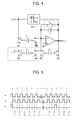
- Fig. 4 shows a circuit with such an additional circuit, along with the quantizer Q ⁇ ⁇ ( ⁇ ) inserted into the feedback path.
- Fig. 4 is a configuration diagram of a first A/D converter based on scale-adjusted ⁇ -map using a switched capacitor integrator circuit of the present invention.
- Fig. 4 shows the SC circuit that realizes the A/D converter based on scale-adjusted ⁇ -map as represented in Equation (16) and Fig. 1 .
- the regions enclosed by the alternate long and short dash lines may be eliminated when applying to the chaos circuit that does not require the set-up of the initial value.
- FIG. 5 shows clocks ⁇ A and ⁇ B to drive the circuit, as well as a clock ⁇ C to simultaneously sample the input signal and reset initial charge of C i .
- Fig. 5 shows a waveform of the three-phase clock to drive the SC circuit in Figs. 4 , 6 , 7 , and 8 .
- L denotes a bit length
- the output bit series b n is sampled at the rising of ⁇ B, i.e. t n+1/2 .
- the bit series obtained from Fig. 4 is -b n .
- C k and C s may be given by Equations (29) and (33) above, respectively.
- the circuit can be simplified as shown in Fig. 6.
- the clock waveform is the same as that shown in Fig. 5 , it is required to combine ⁇ A ⁇ C.
- the regions enclosed by the alternate long and short dash lines may be eliminated when applying to the chaos generator that does not require the set-up of the initial value.
- the clock of ⁇ A ⁇ C may simply utilize ⁇ A.
- C k and C s may be given by Equations (29) and (33) above, respectively.
- the A/D converter based on scale-adjusted ⁇ -map can be realized on the basis of the circuit shown in Fig. 3 .
- Fig. 7 is a configuration diagram of a second A/D converter based on scale-adjusted ⁇ -map using the switched capacitor integrator circuit of the present invention.
- This figure shows the SC circuit that realizes the A/D converter based on scale-adjusted ⁇ -map as represented in Equation (18) and Fig. 2 .
- the regions enclosed by the alternate long and short dash lines may be eliminated when applying to the chaos generator that does not require the set-up of the initial value.
- Fig. 7 shows the circuit in Fig. 3 including an additional circuit to sample the input signal and the quantizer Q ⁇ ⁇ S ⁇ . That is, such a circuit allows realization of the A/D converter based on scale-adjusted ⁇ -map using the SC circuit.
- the clock waveform to drive this circuit is the same as that of the circuits in Figs. 4 and 6 , and is shown in Fig. 5 .
- Equation (34) in order to obtain the decoded value x ⁇ L S of the original signal from the output bit series of L-bits, Equation (34) above may be used.
- Equation (35) when sampling the input signal according to Equation (35) above, C s may be determined as described in Equation (36) above. In this case, Equation (37) above is used to obtain the decoded value x ⁇ L S of the original signal from the output bit series of L-bits.
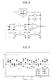
- Fig. 8 is a configuration diagram of a third A/D converter based on scale-adjusted ⁇ -map using the switched capacitor integrator circuit of the present invention, illustrating another method of the SC circuit that realizes the A/D converter based on scale-adjusted ⁇ -map represented in Equation (18) above and Fig. 2 .
- the quantizer Q ⁇ ( ⁇ ) is used, which output controls an input switch of the switched capacitor C i .
- the circuit shown in Fig. 8 would be equivalent to that in Fig. 4 by setting the voltage of the DC voltage source to -1 V. That is, the circuit shown in Fig. 8 serves as well to realize the circuit described in Section [1] above. In this regard, it is also characterized in that the output bit series has no negative sign.
- the regions enclosed in the alternate long and short dash lines are eliminated when applying to the chaos generator that does not require the set-up of the initial value.
- All of the A/D converters based on scale-adjusted ⁇ -map proposed above can be used as is as the chaos generators by extending the bit length L to the infinite. That is, the interval of ⁇ C in Fig. 5 may be extended to ⁇ (here, ⁇ C is a single pulse).
- the circuit to sample the input signal (as enclosed in the alternate long and short dash lines in each figure), as well as the clock ⁇ C, may be eliminated from the circuits shown in Figs. 4 , 6 , and 8 .
- the SPICE simulation using ideal circuit elements is conducted in order to check the validity of the A/D converter circuit based on scale-adjusted ⁇ -map of the present invention.
- the circuit shown in Fig. 8 becomes equivalent to the circuits shown in Figs. 4 , 6, and 7 by adjusting the circuit parameters, so that the simulation was conducted using the circuit in Fig. 8 .
- the value of ⁇ is usually estimated from the bit series after conversion (see Patent Documents 1 and 2, and Non-Patent Documents 1 to 4), the value of ⁇ was assumed to be known because the object here is to check the operation in an ideal condition.
- bit series BS (x input ) output from the circuit is verified whether it coincides with the theoretical value.
- Table 1 shows the comparison of the A/D-converted output bit series for the input signal x input , obtained from the SPICE simulation of the circuit in Fig. 8 and from the theoretical equation.
- bit length L 8. From the table, it can be found that the circuit of the present invention performs the A/D conversion based on scale-adjusted ⁇ -map correctly.
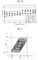
- Fig. 9 shows results of evaluation of the conversion errors for different quantization thresholds ⁇ in each input signal x input .
- Fig. 10 shows results of the conversion errors obtained for different input signals x input while ⁇ is varied. From these results, it was verified that, in the circuit of the present invention, the input signals x input are A/D converted correctly with greater conversion accuracy than the set-up while the quantization threshold ⁇ is varied. In other words, it was verified that the circuit of the present invention has the robustness for variation in ⁇ , which is the characteristic of the A/D conversion based on scale-adjusted ⁇ -map.
- the present invention has been proposed the method of realizing the A/D converter that utilizes the data conversion method based on scale-adjusted ⁇ -map using the discrete time integrator.
- the discrete time integrator is a core circuit element of the analog integrated circuit technology and is used in most cases in the integrated circuits. Accordingly, the A/D converter circuit based on scale-adjusted ⁇ -map of the present invention is considered to be suitable for circuit integration.
- some of specific circuits have also been realized using the switched capacitor circuits as examples.
- the chaos generator According to the present invention, there has been proposed herein to configure the A/D converter that utilizes the data conversion method based on scale-adjusted ⁇ -map as the chaos generator. Since the solution trajectory of the scale-adjusted ⁇ -map is resultantly confined within the finite invariant subinterval, the chaos generator according to the present invention provides the robustness for non-ideal characteristics or noises of the circuit elements along with the stable operation.
- the A/D converter based on scale-adjusted ⁇ -map of the present invention provides the robustness for the change in the circuit characteristics due to the non-ideal characteristics or the like of the circuit elements and noises, so that it can contribute to the realization of compact, low-power-consuming, inexpensive, and highly-efficient A/D converter circuits or chaos generators, in particular to the circuit integration thereof.
- the A/D convertor circuits or chaos generators based on scale-adjusted ⁇ -map of the present invention are suitable even for the semiconductor process on the order of sub-microns or below that is not suited for the integration of analog circuits due to their poor quality of matching or element characteristics of the circuit elements.
- the A/D convertor circuits based on scale-adjusted ⁇ -map of the present invention are applicable to a wide variety of circuits and systems, including various circuits used in systems that operate in the significantly changing environment, such as circuits for large-scale sensor networks, sensor node circuits for sensor dust, node circuits for emergency communications in large-scale disasters, various circuits utilized in the outer space, vehicle-mounted circuits, circuits for mobile robotics, circuits for wireless communication terminals, and the like.
- the chaos generators applying the A/D converter are widely available in the field of cryptology, chaos communications, random number generation, or chaos information processing.
- the present invention should not be limited to the embodiments described above, and a number of variations are possible on the basis of the spirit of the present invention. These variations should not be excluded from the scope of the present invention.
- the data conversion method based on scale-adjusted ⁇ -map of the present invention provides the robustness for the change in environment or circuit characteristics, and contributes to the realization of compact, low-power-consuming, inexpensive, and highly-efficient A/D converter circuits or chaos generators.
Landscapes
- Engineering & Computer Science (AREA)
- Theoretical Computer Science (AREA)
- Compression, Expansion, Code Conversion, And Decoders (AREA)
- Analogue/Digital Conversion (AREA)
Abstract
Description
- The present invention relates to a data conversion method based on scale-adjusted β-map, and particularly to an A/D converter and a chaos generator using a discrete time integrator for adapting to an integrated circuit.
- Conventionally, the data conversion method based on β-map has been proposed (see Non-Patent
Document 1 listed below). This method is, as compared to the PCM (Pulse Code Modulation) method, superior in terms of stability as analog circuits. In other words, in the PCM method, the circuit operation potentially diverges due to the fluctuation or noises of circuit parameters, such as a threshold of a quantizer, a gain constant of a multiply-by-two amplifier. However, the convergence of conversion errors for bit lengths is exponential. On the other hand, in the ∑Δ-type converters, while the circuit operation is stable, the oversampling or the like is required to improve the conversion accuracy. In addition, they take more bit lengths for the convergence of conversion errors. In contrast, the data conversion method based on β-map is robust for mismatches of circuit parameters similar to the ∑Δ-type converters, while it provides the practically optimum rate-distortion characteristics similar to the PCM method. - In recent years, decoding algorithms have been disclosed for minimizing the errors using interval analysis, along with the design principles of circuit parameters, in order to further improve the performance of the data conversion method based on β-map (see
Patent Documents Documents 2 to 4 listed below). Moreover, in order to enhance the degree of freedom of the circuit design, the data conversion method based on scale-adjusted β-map has been proposed that allows the gain β of an amplifier circuit and the threshold of a quantizer to be set up independently (seePatent Document 2, andNon-Patent Documents - In
Patent Documents Non-Patent Documents 1 to 4 listed below, the block diagrams are presented to configure data encoders based on β-map (hereinbelow, A/D converters), the A/D converters based on scale-adjusted β-map, or the like. However, these block diagrams are not suitable for actual implementation of circuits, particularly integrated circuits. - Now, detailed description will be provided.
- The scale-adjusted β-map S (·) is described in Equation (1) (see
Patent Document 2, andNon-Patent Documents 3 and 4). -

wherein, ν □ [s (β - 1), s) is a threshold parameter, 1 < β <2 is a conversion radix, and γ = 1/β, s > 0 is a scaling constant. In addition, when s = (β - 1)-1, the scale-adjusted β-map S (·) is the same as the β-map C (·) below (see Non-Patent Document 1). -

wherein, ν □ [1, (β - 1)-1). Also, when s = β·(β - 1)-1, the scale-adjusted β-map S (·) of Equation (1) above is the same as another β-map D (·) (see Non-Patent Document 1). -

wherein, ν □ [β, β(β - 1)-1). - Assuming that the discrete time is tn (n is a natural number), and then by using it to rewrite Equation (1) above as the one-dimensional discrete time dynamical system, it can be described as

An example of the one-dimensional map is shown inFig. 12 . In this figure, β = 5/3, s = 3, ν = 5/2, and γν = 3/2.Fig. 12 also illustrates the trajectory with x(t1) = 0.6 as an initial value. As shown inFig. 12 , the trajectory is resultantly confined within an invariant subinterval [v - s (β - 1), ν) (the region D inFig. 12 ). - Moreover, a binary variable b(tn) □ {0,1} is defined as

wherein, Qθ (·) is a quantizer with θ as the threshold. Also, the following applies hereinbelow.
At this time, Equation (4) above can be described as
- Here, assume that the input signal xinput is sampled at t = t1. That is,

At this time, by repeating Equation (7) above from t = t1 to t = tL (L is a bit length after A/D conversion), the binary signal train BS (xinput) corresponding to the input signal xinput is obtained. -

wherein, bn = b(tn) (n = 1, 2, ..., L), bL = b(tL) is the LSB (least significant bit), and b1 = b(t1) is the MSB (most significant bit). - Here, the tolerance σν, of the threshold parameter ν of the quantizer Qθ (·) is given as follows with s and β (see
Patent Document 2, andNon-Patent Documents 3 and 4).
This is shown inFig. 12 as the bold line on the axis x(tn+1). Accordingly, the threshold θ of the quantizer is allowed to vary within the range described as follows (seePatent Document 2, andNon-Patent Documents 3 and 4).
This is shown inFig. 12 as the bold line on the axis x(tn). - The configuration diagrams of the A/D converter using the scale-adjusted β-map are shown in
Patent Document 2, and Non-PatentDocuments Fig. 13 shows a configuration diagram of the A/D converter using the scale-adjusted β-map. However, the as-is configuration is not suitable for integrated circuits. -
- Patent Document 1:
WO 2009/014057 - Patent Document 2:
WO 2010/024196 -
- Non-Patent Document 1: I. Daubechies, R. A. DeVore, C. S. Gunturk, and V. A. Vaishampayan, "A/D conversion with imperfect quantizers", IEEE Transactions on Information Theory, Vol. 52, No. 3, pp. 874-885, 2006
- Non-Patent Document 2: S. Hironaka, T. Kohda, and K. Aihara, "Markov chain of binary sequences generated by A/D conversion using β-encoder", in Proceedings of IEEE Workshop on Nonlinear Dynamics of Electronic Systems, pp. 261-264, Tokushima, Japan, 2007
- Non-Patent Document 3: S. Hironaka, T. Kohda, and K. Aihara, "Negative β-encoder", in Proceedings of International Symposium on Nonlinear Theory and Its Applications, pp. 564-567, Budapest, Hungary, 2008
- Non-Patent Document 4: T. Kohda, S. Hironaka, and K. Aihara, "Negative β-encoder", Preprint, arXiv:0808.2548v2[cs.IT], 28 July, 2009, http://arxiv.org/abs/0808.2548
- As described above, there has been a problem that the conventional A/D converters using the scale-adjusted β-map are not suitable for integrated circuits.
- In addition, although the chaos generators using Bernoulli map or Tent map have been proposed as the circuits for generating chaos having uniform distribution of the invariant measure, these circuits have a disadvantage that, when the solution trajectory contacts the ends of a domain, it diverges due to non-ideal characteristics or noises of the circuit, resulting in the unstable operation.
- In view of the circumstances described above, the present invention is directed to provide a data conversion method based on scale-adjusted β-map configured using a discrete time integrator, adapted to integrated circuits and suitable for chaos generators.
- As a specific assembly, there is provided an A/D converter circuit based on scale-adjusted β-map using a switched capacitor (SC) circuit.
- In addition, a chaos generator is proposed that is robust for mismatches or noises of circuit elements and operates stably without trajectory divergence, by extending the bit length of the above-mentioned A/D converter based on scale-adjusted β-map to the infinite because of the fact that the β-map is resultantly confined within an invariant subinterval having a finite trajectory. The proposed chaos generator easily allows realization of different chaos attractors readily only by changing circuit parameters.
- Moreover, the specification checks the operations of the above-mentioned A/D converter circuit based on scale-adjusted β-map and the chaos generator applying thereof to explain their validity by the SPICE (Simulation Program with Integrated Circuit Emphasis) circuit simulation using ideal circuit elements.
- In order to achieve the above-described objects, the present invention provides the following:
[1] A data conversion method based on scale-adjusted β-map including a discrete time integrator, a quantizer connected in series to the discrete time integrator, and a feedback circuit connected from an output of the quantizer to an input of the discrete time integrator. - [2] The data conversion method based on scale-adjusted β-map according to [1] above, wherein an A/D converter is configured of the discrete time integrator having an amplification coefficient s(1 - β) and a damping factor β, and the quantizer Qθ (·).
- [3] The data conversion method based on scale-adjusted β-map according to [1] above, wherein an A/D converter is configured of the discrete time integrator having an amplification coefficient 1 - β and a damping factor β, and the quantizer

- [4] The data conversion method based on scale-adjusted β-map according to [2] or [3] above, wherein the A/D converter is implemented using a switched capacitor integrator circuit.
- [5] The data conversion method based on scale-adjusted β-map according to [2] or [3] above, wherein the A/D converter is configured as a chaos generator by extending a bit length L thereof to the infinite.
- [6] The data conversion method based on scale-adjusted β-map according to any one of [1] to [5] above, wherein a chaotic time series having an initial value xinput is obtained by operating an A/D converter based on scale-adjusted β-map S (·) to sample an input signal xinput at discrete time t1, and repeat the mapping L-times to obtain a conversion bit series BS (xinput) having the bit length L, and by extending the bit length to the infinite (L = ∞) in the operation.
- [7] The data conversion method based on scale-adjusted β-map according to [6] above, wherein, if the initial value is not required to be set up, -∞ < n < ∞ at the discrete time tn is provided wherein the circuit subjected to sampling of the input signal is eliminated to configure a compact chaos generator.
- According to the present invention, the effects as follows can be provided.
- (1) The A/D converter based on scale-adjusted β-map is configured using the discrete time integrator which is a core circuit element in the analog integrated circuit technology and used in most of the integrated circuits. Thus, the A/D converter of the present invention is suitable for circuit integration.
- (2) The A/D converter employing the data conversion method based on scale-adjusted β-map is configured as the chaos generator. A solution trajectory of a scale-adjusted β-map is resultantly confined within a finite invariant subinterval, so that the chaos generator of the present invention is robust for non-ideal characteristics of the circuit elements or noises and operates stably.
-
-
Fig. 1 is a configuration diagram of an A/D converter based on scale-adjusted β-map, illustrating a first embodiment of the present invention; -
Fig. 2 is a configuration diagram of the A/D converter based on scale-adjusted β-map, illustrating a second embodiment of the present invention; -
Fig. 3 shows a typical switched capacitor integrator circuit; -
Fig. 4 is a configuration diagram of a first A/D converter based on scale-adjusted β-map using the switched capacitor integrator circuit of the present invention; -
Fig. 5 is a waveform diagram of a three-phase clock to drive a circuit according to the present invention; -
Fig. 6 is a circuit diagram illustrating the cases where s = (1 - β)-1 (Cf = Cs = Ci) and s = β(1 - β)-1 (Cf = Cs = βCi) inFig. 4 ; -
Fig. 7 is a configuration diagram of a second A/D converter based on scale-adjusted β-map using the switched capacitor integrator circuit of the present invention; -
Fig. 8 is a configuration diagram of a third A/D converter based on scale-adjusted β-map using the switched capacitor integrator circuit of the present invention; -
Fig. 9 shows conversion errors for different quantization thresholds θ when input signals xinput are swept in the circuit inFig. 8 ; -
Fig. 10 shows conversion errors for different input signals xinput when quantization thresholds θ are swept in the circuit inFig. 8 ; -
Fig. 11 shows an exemplary chaos attractor obtained from the SPICE simulation of the circuit inFig. 8 ; -
Fig. 12 shows an exemplary scale-adjusted β-map; and -
Fig. 13 is a configuration diagram of a conventional A/D converter based on scale-adjusted β-map. - A data conversion method based on scale-adjusted β-map of the present invention includes a discrete time integrator, a quantizer connected in series to the discrete time integrator, and a feedback circuit connected from an output of the quantizer to an input of the discrete time integrator.
- Hereinbelow, the embodiments of the present invention will be described in detail.
- For a data conversion method based on scale-adjusted β-map of the present invention, an A/D converter based on scale-adjusted β-map configured using a discrete time integrator will be described.
- The discrete time integrators are used mostly as a major component of an analog integrated circuit. The reasons include that the availability of circuit configuration that is less sensitive to non-ideal characteristics and mismatches of the elements, parasitic elements, or noises, and the ability to further improve the circuit performance with fully-differential circuits. In addition, switched capacitor (SC) circuits, switched current (SI) circuits, and the like are proposed as the integrated circuit technology for discrete time integrator circuits, and the vast knowledge about such circuits has been provided. The availability of such useful data is one of the reasons why the discrete time integrators are used. Therefore, there is proposed the data conversion method based on scale-adjusted β-map wherein the A/D converter using a scale-adjusted β-map is configured with the discrete time integrator.
- First, Z conversion of Equation (7) above results in

wherein, X (z) and B(z) are variables of x (tn) and b (tn) in Z domain, respectively. Moreover, Equation (5) results in
and then, the following is obtained.
Thereby,
and resultantly, the following is obtained.
-
Fig. 1 is a configuration diagram of an A/D converter based on scale-adjusted β-map, illustrating a first embodiment of the present invention. - In this figure,
reference numeral 1 denotes a discrete time integrator, 2 denotes a quantizer connected in series to thediscrete time integrator quantizer 2 to an input of thediscrete time integrator 1. - As shown in
Fig. 1 , it is found that the A/D converter using the scale-adjusted β-map can be realized with thediscrete time integrator 1 having an amplification coefficient s(1 - β) and a damping factor β, and the quantizer 2 [Qθ (·)]. However, an output bit series is given by Equation (9) above.
On the other hand, if the quantizer

Equation (16) above can be rewritten as
In this case, the A/D converter based on scale-adjusted β-map is configured as shown inFig. 2 . -
Fig. 2 is a configuration diagram of the A/D converter based on scale-adjusted β-map, illustrating a second embodiment of the present invention. - In this figure,
reference numeral 11 denotes a discrete time integrator, 12 denotes a quantizer connected in series to thediscrete time integrator quantizer 12 to an input of thediscrete time integrator 11. - As shown in
Fig. 2 , it is found that the A/D converter using the scale-adjusted β-map can be realized with thediscrete time integrator 11 having an amplification coefficient 1 - β and a damping factor β, and the quantizer 12


- Next, a chaos generator employing the data conversion method based on scale-adjusted β-map will be described.
- As described above, there has been a problem about the previously proposed chaos generators using Bernoulli map or Tent map that, when the solution trajectory contacts the ends of a domain, it diverges due to non-ideal characteristics or noises of the circuit, resulting in the unstable operation. Thus, the chaos generator that operates stably is proposed herein, utilizing the fact that the solution trajectory of a scale-adjusted β-map S (·) is resultantly confined within a finite invariant subinterval.
- The solution trajectory of the scale-adjusted β-map S (·) is, after the transient status, trapped in an invariant subinterval [ν - s(β - 1), ν) shown as D in
Fig. 12 . Thus, if that the width of trajectory shift due to non-ideal characteristics or noises of the circuit element is defined as δdeviation, the solution trajectory does not contact the ends (0 and s) of a domain x(tn) in a range of ν values of S(β - 1) + δdeviation < ν < s - δdeviation. As such, the solution trajectory does not diverge due to the effect of non-ideal characteristics or noises of the circuit, and the chaos generator operates stably. In addition, invariant measure is distributed uniformly in the invariant subinterval of a chaos trajectory realized by the β-map S (·), so that the resultant chaotic time series is considered to be readily applied to random number generation, encryption, and the like. - Next, a method of configuring the chaos generator with the scale-adjusted β-map S (·) will be described specifically. In the A/D converter based on scale-adjusted β-map S (·) described above, the operation of sampling the input signal xinput at the discrete time t1 and repeating the mapping L-times results in a conversion bit series BS (xinput) having a bit length of L. In this operation, extending the bit length to the infinite (L = ∞) enables obtaining the chaotic time series having an initial value of xinput. Thereby, the A/D converter using the scale-adjusted β-map utilizing the discrete time integrator described above can be applied as is as the chaos generator. In addition, if the initial value is not required to be set up, -∞ < n < ∞ may be applied at the discrete time tn. In this case, the A/D converter based on scale-adjusted β-map utilizing the discrete time integrator described above can eliminate the element for sampling the input signal, so that the more compact chaos generator can be realized.
- Next, as an embodiment of the present invention, an exemplary circuit of the A/D converter based on scale-adjusted β-map utilizing the switched capacitor (SC) will be described.
- The major technology of discrete time analog circuits (sampled data circuits) includes the SC circuits and the SI (switched current) circuits. Here, a method will be described to realize the A/D converter circuit based on scale-adjusted β-map utilizing the SC circuit. In this regard, note that the circuit can also be realized in a similar manner using the SI circuit. Specifically, the method will be described to implement the A/D converter circuit using the scale-adjusted β-map given in Equation (16) and
Fig. 1 or Equation (18) andFig. 2 , utilizing an SC integrator circuit. - [1] Circuit example 1 utilizing SC circuit: the case using Equation (16) and
Fig. 1
Fig. 3 shows a typical switched capacitor (SC) integrator circuit. The transfer function in the Z domain of this circuit is given by:
Where, V0 (z) and Vi (z) are variables of ν0 (tn) and νi(tn) in the Z domain, respectively. It is found that, by comparing Equations (16) and (20),



may be applied. However, since -1 < 1 - β < 0 is derived from 1 < β < 2 and thus the capacitor ratio becomes negative in Equation (22) above, it is physically infeasible. - Thus, the quantizer

having a negative sign on the output is introduced. Using this, Equation (16) above can be transformed as
As the result, if the conditions



are satisfied in the circuit shown inFig. 3 , the A/D converter based on scale-adjusted β-map can be realized from the circuit inFig. 3 and the quantizer Q̃θ (·).
In this regard, since the circuit inFig. 3 does not include a circuit to input the input signal xinput, there is a need to add a circuit inFig. 3 to sample the input signal.Fig. 4 shows a circuit with such an additional circuit, along with the quantizer Q̃θ (·) inserted into the feedback path. -
Fig. 4 is a configuration diagram of a first A/D converter based on scale-adjusted β-map using a switched capacitor integrator circuit of the present invention. -
Fig. 4 shows the SC circuit that realizes the A/D converter based on scale-adjusted β-map as represented in Equation (16) andFig. 1 . Here, the regions enclosed by the alternate long and short dash lines may be eliminated when applying to the chaos circuit that does not require the set-up of the initial value. - Moreover,
Fig. 5 shows clocks ϕA and ϕB to drive the circuit, as well as a clock ϕC to simultaneously sample the input signal and reset initial charge of Ci. -
Fig. 5 shows a waveform of the three-phase clock to drive the SC circuit inFigs. 4 ,6 ,7 , and8 . In this figure, L denotes a bit length, and the output bit series bn is sampled at the rising of ϕB, i.e. tn+1/2. - Here, if the input signal is sampled according to Equation (8) above, a most significant bit b1 is

On the other hand, when the input signal is sampled at t1 as shown inFig. 5 and b1 is output at t1+1/2 in the circuit inFig. 4 , the transfer function of the circuit in that case is
By comparing Equations (31) and (32) above, it can be found that, if the input signal is sampled according to Equation (8) above in the circuit inFig. 4 ,
may be applied. In this case, in order to obtain a decoded value x̂L of an original signal from the output bit series of L-bits,
may be applied (seePatent Document 2 andNon-Patent Documents 3 and 4). However, it should be noted that the bit series obtained fromFig. 4 is -bn. - Meanwhile, as shown in
Fig. 13 , when sampling the input signal as
the following may be applied.
In this case, in order to obtain the decoded value x̂L of the original signal from the output bit series of L-bits,
may be applied considering that the input signal xinput is initially multiplied by β. However, it should also be noted that the bit series obtained from the circuit shown inFig. 4 is -bn. - Hereinbefore, it has been illustrated that the A/D converter based on scale-adjusted β-map represented in Equation (16) and
Fig. 1 can be realized using the SC circuit shown inFig. 4 . Next, the circuit configuration will be described in the case where s has a certain value. - In this case, the scale-adjusted β-map S (·) would be the β-map C (·) given by Equation (2) above. In
Fig. 4 , Equation (28) gives
In this case, Ck and Cs may be given by Equations (29) and (33) above, respectively. This results in
so that Cf and Cs can be shared in the circuit inFig. 4 . Thus, the circuit can be simplified as shown inFig. 6. Fig. 6 shows a circuit in the cases where s = (1 - β)-1 (Cf = Cs = Ci) and s = β(1 - β)-1 (Cf = Cs = βCi) (described below) inFig. 4 . Although the clock waveform is the same as that shown inFig. 5 , it is required to combine ϕA·ϕC. Here, the regions enclosed by the alternate long and short dash lines may be eliminated when applying to the chaos generator that does not require the set-up of the initial value. Also, in this regard, the clock of ϕA·ϕC may simply utilize ϕA. - In this case, the scale-adjusted β-map S (·) would be the β-map D (·) given by Equation (3) above. In
Fig. 4 , Equation (28) gives
In this case, Ck and Cs may be given by Equations (29) and (33) above, respectively. - Although this still does not make it possible to simplify
Fig. 4 , Cs is given by Equation (36) above if the input is sampled as described by Equation (35) above, so that Cf and Cs can be shared in the circuit inFig. 4 as with Example (a) described above. Accordingly, the simplified circuit as shown inFig. 6 can also be used. However,
Moreover, it is required to use Equation (37) above for the decoding. - In the method described above in Section [1], the value of Cf is a function of s and β, introducing the constraint on the degree of freedom of the circuit design. Therefore, in order to enhance the degree of freedom of the circuit design, the method of circuit configuration is proposed here, wherein the circuit parameter only depends on either s or β.
- It is found from the comparison between the transfer function of the SC integrator circuit in
Fig. 3 [Equation (20)] and Equation (18) that, if



are applied, the A/D converter using the scale-adjusted β-map can be realized utilizing the circuit inFig. 3 . However, as described above in Section [1],
and the negative capacitor ratio is physically infeasible. As such, as with Section [1] above, the quantizer
having a negative sign on the output is introduced. Using this, Equation (18) above can be transformed as
As a result, if the conditions


are satisfied in the circuit shown inFig. 7 , the A/D converter based on scale-adjusted β-map can be realized on the basis of the circuit shown inFig. 3 . -
Fig. 7 is a configuration diagram of a second A/D converter based on scale-adjusted β-map using the switched capacitor integrator circuit of the present invention. This figure shows the SC circuit that realizes the A/D converter based on scale-adjusted β-map as represented in Equation (18) andFig. 2 . Here, the regions enclosed by the alternate long and short dash lines may be eliminated when applying to the chaos generator that does not require the set-up of the initial value. - As with Section [1] described above,
Fig. 7 shows the circuit inFig. 3 including an additional circuit to sample the input signal and the quantizer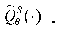
Figs. 4 and6 , and is shown inFig. 5 .
Here, if the input signal is sampled according to Equation (8) above, the most significant bit

On the other hand, if the input signal of the circuit inFig. 7 is sampled at t1 as shown inFig. 5 and

Therefore, in comparison between Equations (53) and (54) above, it is found that Cs may be determined in the circuit inFig. 7 as described in Equation (33). In this case, in order to obtain the decoded value

On the other hand, as shown inFig. 13 , when sampling the input signal according to Equation (35) above, Cs may be determined as described in Equation (36) above. In this case, Equation (37) above is used to obtain the decoded value
- Meanwhile, the additional quantizer

Fig. 7 . However, by changing the switch control on the left side of Cf inFig. 4 to be controlled by the output of the quantizer and introducing a DC voltage source of -s V, the circuit equivalent to that inFig. 7 can be realized. Such a circuit is shown inFig. 8 .
Fig. 8 is a configuration diagram of a third A/D converter based on scale-adjusted β-map using the switched capacitor integrator circuit of the present invention, illustrating another method of the SC circuit that realizes the A/D converter based on scale-adjusted β-map represented in Equation (18) above andFig. 2 . In the circuit inFig. 8 , the quantizer Qθ (·) is used, which output controls an input switch of the switched capacitor Ci. A control signal P thereof is P = bn·ϕA, and the output bit series is bn having no negative sign. - On the other hand, the circuit shown in
Fig. 8 would be equivalent to that inFig. 4 by setting the voltage of the DC voltage source to -1 V. That is, the circuit shown inFig. 8 serves as well to realize the circuit described in Section [1] above. In this regard, it is also characterized in that the output bit series has no negative sign. Here, the regions enclosed in the alternate long and short dash lines are eliminated when applying to the chaos generator that does not require the set-up of the initial value. - All of the A/D converters based on scale-adjusted β-map proposed above can be used as is as the chaos generators by extending the bit length L to the infinite. That is, the interval of ϕC in
Fig. 5 may be extended to ∞ (here, ϕC is a single pulse). - Furthermore, if the initial value of the chaotic time series is not required to be set up, the circuit to sample the input signal (as enclosed in the alternate long and short dash lines in each figure), as well as the clock ϕC, may be eliminated from the circuits shown in
Figs. 4 ,6 , and8 . - Next, the SPICE simulation using ideal circuit elements is conducted in order to check the validity of the A/D converter circuit based on scale-adjusted β-map of the present invention. Here, the circuit shown in
Fig. 8 becomes equivalent to the circuits shown inFigs. 4 ,6, and 7 by adjusting the circuit parameters, so that the simulation was conducted using the circuit inFig. 8 . In addition, although the value of β is usually estimated from the bit series after conversion (seePatent Documents Non-Patent Documents 1 to 4), the value of β was assumed to be known because the object here is to check the operation in an ideal condition. Here, note that β = 5/3, s = 3 in the following simulation. - First, the bit series BS (xinput) output from the circuit is verified whether it coincides with the theoretical value. Table 1 shows the comparison of the A/D-converted output bit series for the input signal xinput, obtained from the SPICE simulation of the circuit in
Fig. 8 and from the theoretical equation. Here, the bit length L = 8. From the table, it can be found that the circuit of the present invention performs the A/D conversion based on scale-adjusted β-map correctly. -
Table 1 Input Quantization threshold Output bit series BS (xinput) xinput θ SPICE Theoretical value Error 0.1 1.21 00001000 00001000 0 1.5 00000110 00000110 0 1.79 00000101 00000101 0 0.5 1.21 01000100 01000100 0 1.5 00110101 00110101 0 1.79 00110100 00110100 0 0.95 1.21 10010100 10010100 0 1.5 10010100 10010100 0 1.79 01110101 01110101 0 - Next, the evaluation is conducted of the conversion error of the decoded value of the output bit series obtained from the SPICE simulation of the circuit shown in
Fig. 8 . When the conversion bit length is L, the upper bound of the quantization error is given by
Using this, the bit length L = 13 is adopted to provide εL(x) ≤ 2-9 . -
Fig. 9 shows results of evaluation of the conversion errors for different quantization thresholds θ in each input signal xinput.Fig. 10 shows results of the conversion errors obtained for different input signals xinput while θ is varied. From these results, it was verified that, in the circuit of the present invention, the input signals xinput are A/D converted correctly with greater conversion accuracy than the set-up while the quantization threshold θ is varied. In other words, it was verified that the circuit of the present invention has the robustness for variation in θ, which is the characteristic of the A/D conversion based on scale-adjusted β-map. - Furthermore, in the circuit shown in
Fig. 8 , the chaos generator was realized with the bit length L = ∞.Fig. 11 shows an exemplary chaos attractor obtained from the SPICE simulation when θ = 1.44. FromFig. 11 , it is found that the chaos attractor remains within the invariant subinterval (v - s(β-1) = 0.4 ≤ x (tn) ≤ ν = 2.4). - As described above, the present invention has been proposed the method of realizing the A/D converter that utilizes the data conversion method based on scale-adjusted β-map using the discrete time integrator. The discrete time integrator is a core circuit element of the analog integrated circuit technology and is used in most cases in the integrated circuits. Accordingly, the A/D converter circuit based on scale-adjusted β-map of the present invention is considered to be suitable for circuit integration. Herein, some of specific circuits have also been realized using the switched capacitor circuits as examples.
- Moreover, there has been proposed herein to configure the A/D converter that utilizes the data conversion method based on scale-adjusted β-map as the chaos generator. Since the solution trajectory of the scale-adjusted β-map is resultantly confined within the finite invariant subinterval, the chaos generator according to the present invention provides the robustness for non-ideal characteristics or noises of the circuit elements along with the stable operation.
- Finally, with the SPICE circuit simulation using the ideal circuit elements, the checking has been conducted on the operation of the A/D converter circuit that utilizes the data conversion method based on scale-adjusted β-map of the present invention to verify its validity.
- The A/D converter based on scale-adjusted β-map of the present invention provides the robustness for the change in the circuit characteristics due to the non-ideal characteristics or the like of the circuit elements and noises, so that it can contribute to the realization of compact, low-power-consuming, inexpensive, and highly-efficient A/D converter circuits or chaos generators, in particular to the circuit integration thereof. In addition, in terms of circuit integration, the A/D convertor circuits or chaos generators based on scale-adjusted β-map of the present invention are suitable even for the semiconductor process on the order of sub-microns or below that is not suited for the integration of analog circuits due to their poor quality of matching or element characteristics of the circuit elements. Moreover, the A/D convertor circuits based on scale-adjusted β-map of the present invention are applicable to a wide variety of circuits and systems, including various circuits used in systems that operate in the significantly changing environment, such as circuits for large-scale sensor networks, sensor node circuits for sensor dust, node circuits for emergency communications in large-scale disasters, various circuits utilized in the outer space, vehicle-mounted circuits, circuits for mobile robotics, circuits for wireless communication terminals, and the like. Furthermore, the chaos generators applying the A/D converter are widely available in the field of cryptology, chaos communications, random number generation, or chaos information processing.
The present invention should not be limited to the embodiments described above, and a number of variations are possible on the basis of the spirit of the present invention. These variations should not be excluded from the scope of the present invention. - The data conversion method based on scale-adjusted β-map of the present invention provides the robustness for the change in environment or circuit characteristics, and contributes to the realization of compact, low-power-consuming, inexpensive, and highly-efficient A/D converter circuits or chaos generators.
Claims (7)
- A data conversion method based on scale-adjusted β-map comprising:a discrete time integrator;a quantizer connected in series to the discrete time integrator; anda feedback circuit connected from an output of the quantizer to an input of the discrete time integrator.
- The data conversion method based on scale-adjusted β-map according to claim 1, wherein an A/D converter is configured of the discrete time integrator having an amplification coefficient s(1 - β) and a damping factor β, and the quantizer Qθ (·).
- The data conversion method based on scale-adjusted β-map according to claim 1, wherein an A/D converter is configured of the discrete time integrator having an amplification coefficient 1 - β and a damping factor β, and the quantizer

- The data conversion method based on scale-adjusted β-map according to claim 2 or 3, wherein the A/D converter is implemented using a switched capacitor integrator circuit.
- The data conversion method based on scale-adjusted β-map according to claim 2 or 3, wherein the A/D converter is configured as a chaos generator by extending a bit length L thereof to the infinite.
- The data conversion method based on scale-adjusted β-map according to any one of claims 1 to 5, wherein a chaotic time series having an initial value xinput is obtained by operating an A/D converter based on scale-adjusted β-map S
(·) to sample an input signal xinput at discrete time t1, and repeat the mapping L-times to obtain a conversion bit series BS (xinput) having the bit length L, and by extending the bit length to the infinite (L = ∞) in the operation. - The data conversion method based on scale-adjusted β-map according to claim 6, wherein, if the initial value is not required to be set up, -∞ < n < ∞ at the discrete time tn is provided wherein the circuit subjected to sampling of the input signal is eliminated to configure a compact chaos generator.
Applications Claiming Priority (2)
| Application Number | Priority Date | Filing Date | Title |
|---|---|---|---|
| JP2010085212 | 2010-04-01 | ||
| PCT/JP2011/001664 WO2011125296A1 (en) | 2010-04-01 | 2011-03-22 | DATA CONVERSION METHOD BASED ON SCALE-ADJUSTED β-MAP |
Publications (2)
| Publication Number | Publication Date |
|---|---|
| EP2555433A1 true EP2555433A1 (en) | 2013-02-06 |
| EP2555433A4 EP2555433A4 (en) | 2014-06-04 |
Family
ID=44762267
Family Applications (1)
| Application Number | Title | Priority Date | Filing Date |
|---|---|---|---|
| EP11765198.4A Withdrawn EP2555433A4 (en) | 2010-04-01 | 2011-03-22 | METHOD OF CONVERTING DATA BASED ON -MAP SCALE |
Country Status (4)
| Country | Link |
|---|---|
| US (1) | US8773295B2 (en) |
| EP (1) | EP2555433A4 (en) |
| JP (1) | JP5334225B2 (en) |
| WO (1) | WO2011125296A1 (en) |
Families Citing this family (8)
| Publication number | Priority date | Publication date | Assignee | Title |
|---|---|---|---|---|
| JP6422073B2 (en) * | 2014-08-06 | 2018-11-14 | 東芝情報システム株式会社 | A / D conversion circuit |
| KR20160029525A (en) * | 2014-09-05 | 2016-03-15 | 삼성전자주식회사 | Method of controlling user interface and electronic device supporting the same |
| JP6833643B2 (en) * | 2017-09-07 | 2021-02-24 | 東芝情報システム株式会社 | Compression processing device, decompression processing device, compression processing program, decompression processing program |
| WO2019237115A1 (en) | 2018-06-08 | 2019-12-12 | Cohen Seth D | Clockless time-to-digital converter |
| US11381224B2 (en) | 2018-06-08 | 2022-07-05 | Southern Research Institute | Clockless programmable pulse width generation using an inverse chaotic map |
| US11265178B1 (en) | 2018-06-08 | 2022-03-01 | Southern Research Institute | Physically unclonable functions using pulse width chaotic maps |
| KR102197791B1 (en) * | 2018-12-13 | 2021-01-04 | 인제대학교 산학협력단 | Novel wideband chaotic approach lna with microcontroller compatibility and 5g wireless secure communication device using thereof |
| US11733364B2 (en) | 2020-05-21 | 2023-08-22 | Kratos Sre, Inc. | Target ranging with subsampled noise correlation |
Family Cites Families (5)
| Publication number | Priority date | Publication date | Assignee | Title |
|---|---|---|---|---|
| US5644308A (en) * | 1995-01-17 | 1997-07-01 | Crystal Semiconductor Corporation | Algorithmic analog-to-digital converter having redundancy and digital calibration |
| US6452524B1 (en) * | 2001-02-08 | 2002-09-17 | Ericsson Inc. | Delta sigma converter incorporating a multiplier |
| US7057540B2 (en) * | 2001-10-26 | 2006-06-06 | Texas Instruments Incorporated | Sigma-delta (ΣΔ) analog-to-digital converter (ADC) structure incorporating a direct sampling mixer |
| EP2169832A4 (en) | 2007-07-20 | 2012-07-25 | Japan Science & Tech Agency | CONVERTER, CONVERSION METHOD, PROGRAM, AND RECORDING MEDIUM |
| US20110193734A1 (en) * | 2008-08-25 | 2011-08-11 | Japan Science And Technology Agency | Signal converter, parameter deciding device, parameter deciding method, program, and recording medium |
-
2011
- 2011-03-22 EP EP11765198.4A patent/EP2555433A4/en not_active Withdrawn
- 2011-03-22 US US13/638,140 patent/US8773295B2/en not_active Expired - Fee Related
- 2011-03-22 WO PCT/JP2011/001664 patent/WO2011125296A1/en not_active Ceased
- 2011-03-22 JP JP2012509297A patent/JP5334225B2/en not_active Expired - Fee Related
Also Published As
| Publication number | Publication date |
|---|---|
| JP5334225B2 (en) | 2013-11-06 |
| JPWO2011125296A1 (en) | 2013-07-08 |
| US8773295B2 (en) | 2014-07-08 |
| US20130015992A1 (en) | 2013-01-17 |
| EP2555433A4 (en) | 2014-06-04 |
| WO2011125296A1 (en) | 2011-10-13 |
Similar Documents
| Publication | Publication Date | Title |
|---|---|---|
| US8773295B2 (en) | Data conversion method based on scale-adjusted B-map | |
| EP2557693B1 (en) | Data conversion method based on negative beta-map | |
| US7852253B2 (en) | Digitally adjustable quantization circuit | |
| US7501965B2 (en) | Correcting for errors that cause generated digital codes to deviate from expected values in an ADC | |
| US12206425B2 (en) | Linearization of digital-to-analog converters (DACs) and analog-to-digital converters (ADCs) and associated methods | |
| US9397691B2 (en) | Mostly-digital open-loop ring oscillator delta-sigma ADC and methods for conversion | |
| CN105391450A (en) | Efficient analog to digital converter | |
| US7379009B2 (en) | AD converter and radio receiver | |
| US6989778B2 (en) | Semi-conductor circuit arrangement | |
| JP5758434B2 (en) | ΔΣ A / D converter | |
| CN1411629A (en) | Improved current-steering D/A conversion | |
| US20120092202A1 (en) | Analog to digital converter | |
| Yu et al. | A two-step ADC with statistical calibration | |
| US6469646B1 (en) | Converting digital signals to analog signals | |
| EP2320571A1 (en) | Signal converter, parameter deciding device, parameter deciding method, program, and recording medium | |
| US7986258B2 (en) | Analog-digital conversion cell and analog-digital converter | |
| WO2007015714A2 (en) | Analog-to-digital converter | |
| Ignjatovic et al. | Information-theoretic approach to a/d conversion | |
| RU2741062C1 (en) | Method for injector decoding of convolution codes | |
| Chung et al. | A 3.3 V 10 bit current-mode folding and interpolating CMOS A/D converter using an arithmetic functionality | |
| Heydenreich et al. | Functionals of brownian bridges arising in the current mismatch in D/A converters | |
| KR20010096396A (en) | Analog-to-digital converter with a folding multiplier | |
| Scandurra et al. | Design and realization of high-accuracy static analog memories (SAMs) using low-cost DA converters | |
| CN106130552A (en) | A kind of pipelined analog-digital converter | |
| El Rachini | Redundant analog to digital conversion architectures in CMOS technology |
Legal Events
| Date | Code | Title | Description |
|---|---|---|---|
| PUAI | Public reference made under article 153(3) epc to a published international application that has entered the european phase |
Free format text: ORIGINAL CODE: 0009012 |
|
| 17P | Request for examination filed |
Effective date: 20121008 |
|
| AK | Designated contracting states |
Kind code of ref document: A1 Designated state(s): AL AT BE BG CH CY CZ DE DK EE ES FI FR GB GR HR HU IE IS IT LI LT LU LV MC MK MT NL NO PL PT RO RS SE SI SK SM TR |
|
| RIN1 | Information on inventor provided before grant (corrected) |
Inventor name: JINNO, KENYA Inventor name: HORIO, YOSHIHIKO Inventor name: KOHDA, TOHRU Inventor name: AIHARA, KAZUYUKI |
|
| DAX | Request for extension of the european patent (deleted) | ||
| A4 | Supplementary search report drawn up and despatched |
Effective date: 20140508 |
|
| RIC1 | Information provided on ipc code assigned before grant |
Ipc: H03M 1/06 20060101AFI20140425BHEP Ipc: H03M 1/40 20060101ALN20140425BHEP Ipc: G06F 7/58 20060101ALN20140425BHEP |
|
| STAA | Information on the status of an ep patent application or granted ep patent |
Free format text: STATUS: THE APPLICATION HAS BEEN WITHDRAWN |
|
| 18W | Application withdrawn |
Effective date: 20190913 |