EP2555314B1 - Photoelectrochemical cell and energy system using same - Google Patents
Photoelectrochemical cell and energy system using same Download PDFInfo
- Publication number
- EP2555314B1 EP2555314B1 EP11762184.7A EP11762184A EP2555314B1 EP 2555314 B1 EP2555314 B1 EP 2555314B1 EP 11762184 A EP11762184 A EP 11762184A EP 2555314 B1 EP2555314 B1 EP 2555314B1
- Authority
- EP
- European Patent Office
- Prior art keywords
- semiconductor layer
- semiconductor
- level
- band
- conductor
- Prior art date
- Legal status (The legal status is an assumption and is not a legal conclusion. Google has not performed a legal analysis and makes no representation as to the accuracy of the status listed.)
- Not-in-force
Links
- 239000004065 semiconductor Substances 0.000 claims description 517
- 239000004020 conductor Substances 0.000 claims description 111
- 239000001257 hydrogen Substances 0.000 claims description 62
- 229910052739 hydrogen Inorganic materials 0.000 claims description 62
- UFHFLCQGNIYNRP-UHFFFAOYSA-N Hydrogen Chemical compound [H][H] UFHFLCQGNIYNRP-UHFFFAOYSA-N 0.000 claims description 60
- 239000003792 electrolyte Substances 0.000 claims description 43
- 238000003860 storage Methods 0.000 claims description 19
- QCWXUUIWCKQGHC-UHFFFAOYSA-N Zirconium Chemical compound [Zr] QCWXUUIWCKQGHC-UHFFFAOYSA-N 0.000 claims description 16
- 229910052788 barium Inorganic materials 0.000 claims description 16
- DSAJWYNOEDNPEQ-UHFFFAOYSA-N barium atom Chemical compound [Ba] DSAJWYNOEDNPEQ-UHFFFAOYSA-N 0.000 claims description 16
- 229910052738 indium Inorganic materials 0.000 claims description 16
- APFVFJFRJDLVQX-UHFFFAOYSA-N indium atom Chemical compound [In] APFVFJFRJDLVQX-UHFFFAOYSA-N 0.000 claims description 16
- 229910052726 zirconium Inorganic materials 0.000 claims description 16
- 239000000470 constituent Substances 0.000 claims description 14
- 239000000446 fuel Substances 0.000 claims description 13
- 229910052684 Cerium Inorganic materials 0.000 claims description 8
- 206010021143 Hypoxia Diseases 0.000 claims description 4
- 230000005611 electricity Effects 0.000 claims description 4
- GWXLDORMOJMVQZ-UHFFFAOYSA-N cerium Chemical compound [Ce] GWXLDORMOJMVQZ-UHFFFAOYSA-N 0.000 claims 2
- 239000010410 layer Substances 0.000 description 366
- 239000000463 material Substances 0.000 description 45
- 230000000052 comparative effect Effects 0.000 description 35
- 239000010408 film Substances 0.000 description 25
- 238000006243 chemical reaction Methods 0.000 description 22
- GWEVSGVZZGPLCZ-UHFFFAOYSA-N Titan oxide Chemical compound O=[Ti]=O GWEVSGVZZGPLCZ-UHFFFAOYSA-N 0.000 description 19
- XLYOFNOQVPJJNP-UHFFFAOYSA-N water Substances O XLYOFNOQVPJJNP-UHFFFAOYSA-N 0.000 description 19
- 230000004888 barrier function Effects 0.000 description 15
- 239000007789 gas Substances 0.000 description 14
- 238000000034 method Methods 0.000 description 14
- 230000001443 photoexcitation Effects 0.000 description 14
- 239000000203 mixture Substances 0.000 description 13
- 239000010409 thin film Substances 0.000 description 12
- 230000001699 photocatalysis Effects 0.000 description 11
- OGIDPMRJRNCKJF-UHFFFAOYSA-N titanium oxide Inorganic materials [Ti]=O OGIDPMRJRNCKJF-UHFFFAOYSA-N 0.000 description 11
- 239000011941 photocatalyst Substances 0.000 description 10
- 230000006798 recombination Effects 0.000 description 10
- 238000005215 recombination Methods 0.000 description 10
- QVGXLLKOCUKJST-UHFFFAOYSA-N atomic oxygen Chemical compound [O] QVGXLLKOCUKJST-UHFFFAOYSA-N 0.000 description 9
- 239000002585 base Substances 0.000 description 9
- 238000004070 electrodeposition Methods 0.000 description 9
- 239000011521 glass Substances 0.000 description 9
- 239000001301 oxygen Substances 0.000 description 9
- 229910052760 oxygen Inorganic materials 0.000 description 9
- 238000009413 insulation Methods 0.000 description 8
- 238000000926 separation method Methods 0.000 description 8
- 239000000758 substrate Substances 0.000 description 8
- 239000010936 titanium Substances 0.000 description 8
- 238000005452 bending Methods 0.000 description 7
- BASFCYQUMIYNBI-UHFFFAOYSA-N platinum Substances [Pt] BASFCYQUMIYNBI-UHFFFAOYSA-N 0.000 description 7
- ZMIGMASIKSOYAM-UHFFFAOYSA-N cerium Chemical compound [Ce][Ce][Ce][Ce][Ce][Ce][Ce][Ce][Ce][Ce][Ce][Ce][Ce][Ce][Ce][Ce][Ce][Ce][Ce][Ce][Ce][Ce][Ce][Ce][Ce][Ce][Ce][Ce][Ce][Ce][Ce][Ce][Ce][Ce][Ce][Ce][Ce][Ce] ZMIGMASIKSOYAM-UHFFFAOYSA-N 0.000 description 6
- 238000005259 measurement Methods 0.000 description 6
- 238000004544 sputter deposition Methods 0.000 description 5
- 150000001875 compounds Chemical class 0.000 description 4
- 238000010586 diagram Methods 0.000 description 4
- 230000000694 effects Effects 0.000 description 4
- 238000005868 electrolysis reaction Methods 0.000 description 4
- 238000002474 experimental method Methods 0.000 description 4
- 238000004458 analytical method Methods 0.000 description 3
- 230000001678 irradiating effect Effects 0.000 description 3
- 238000004519 manufacturing process Methods 0.000 description 3
- 150000004767 nitrides Chemical class 0.000 description 3
- 239000005518 polymer electrolyte Substances 0.000 description 3
- 239000007787 solid Substances 0.000 description 3
- 238000004402 ultra-violet photoelectron spectroscopy Methods 0.000 description 3
- 238000000870 ultraviolet spectroscopy Methods 0.000 description 3
- 238000010521 absorption reaction Methods 0.000 description 2
- 239000007864 aqueous solution Substances 0.000 description 2
- 239000000969 carrier Substances 0.000 description 2
- 239000011247 coating layer Substances 0.000 description 2
- 239000002131 composite material Substances 0.000 description 2
- BERDEBHAJNAUOM-UHFFFAOYSA-N copper(I) oxide Inorganic materials [Cu]O[Cu] BERDEBHAJNAUOM-UHFFFAOYSA-N 0.000 description 2
- KRFJLUBVMFXRPN-UHFFFAOYSA-N cuprous oxide Chemical compound [O-2].[Cu+].[Cu+] KRFJLUBVMFXRPN-UHFFFAOYSA-N 0.000 description 2
- 238000007599 discharging Methods 0.000 description 2
- VDQVEACBQKUUSU-UHFFFAOYSA-M disodium;sulfanide Chemical compound [Na+].[Na+].[SH-] VDQVEACBQKUUSU-UHFFFAOYSA-M 0.000 description 2
- -1 hydrogen ions Chemical class 0.000 description 2
- 229910052751 metal Inorganic materials 0.000 description 2
- 239000002184 metal Substances 0.000 description 2
- 229910021645 metal ion Inorganic materials 0.000 description 2
- 150000002739 metals Chemical class 0.000 description 2
- 229910052758 niobium Inorganic materials 0.000 description 2
- 229910052697 platinum Inorganic materials 0.000 description 2
- 239000000843 powder Substances 0.000 description 2
- 239000011347 resin Substances 0.000 description 2
- 229920005989 resin Polymers 0.000 description 2
- 229910052979 sodium sulfide Inorganic materials 0.000 description 2
- GEHJYWRUCIMESM-UHFFFAOYSA-L sodium sulfite Chemical compound [Na+].[Na+].[O-]S([O-])=O GEHJYWRUCIMESM-UHFFFAOYSA-L 0.000 description 2
- 239000007784 solid electrolyte Substances 0.000 description 2
- 239000000243 solution Substances 0.000 description 2
- 229910052719 titanium Inorganic materials 0.000 description 2
- OYPRJOBELJOOCE-UHFFFAOYSA-N Calcium Chemical compound [Ca] OYPRJOBELJOOCE-UHFFFAOYSA-N 0.000 description 1
- RWSOTUBLDIXVET-UHFFFAOYSA-N Dihydrogen sulfide Chemical compound S RWSOTUBLDIXVET-UHFFFAOYSA-N 0.000 description 1
- 229910052688 Gadolinium Inorganic materials 0.000 description 1
- GYHNNYVSQQEPJS-UHFFFAOYSA-N Gallium Chemical compound [Ga] GYHNNYVSQQEPJS-UHFFFAOYSA-N 0.000 description 1
- HBBGRARXTFLTSG-UHFFFAOYSA-N Lithium ion Chemical compound [Li+] HBBGRARXTFLTSG-UHFFFAOYSA-N 0.000 description 1
- 229920000557 Nafion® Polymers 0.000 description 1
- RTAQQCXQSZGOHL-UHFFFAOYSA-N Titanium Chemical compound [Ti] RTAQQCXQSZGOHL-UHFFFAOYSA-N 0.000 description 1
- 229910052769 Ytterbium Inorganic materials 0.000 description 1
- 238000000862 absorption spectrum Methods 0.000 description 1
- 230000002378 acidificating effect Effects 0.000 description 1
- 239000003513 alkali Substances 0.000 description 1
- 230000005540 biological transmission Effects 0.000 description 1
- 230000000903 blocking effect Effects 0.000 description 1
- 229910052791 calcium Inorganic materials 0.000 description 1
- 239000011575 calcium Substances 0.000 description 1
- 150000004770 chalcogenides Chemical class 0.000 description 1
- 229910052804 chromium Inorganic materials 0.000 description 1
- 239000011248 coating agent Substances 0.000 description 1
- 238000000576 coating method Methods 0.000 description 1
- 230000007423 decrease Effects 0.000 description 1
- 230000003247 decreasing effect Effects 0.000 description 1
- 239000013505 freshwater Substances 0.000 description 1
- UIWYJDYFSGRHKR-UHFFFAOYSA-N gadolinium atom Chemical compound [Gd] UIWYJDYFSGRHKR-UHFFFAOYSA-N 0.000 description 1
- 229910052733 gallium Inorganic materials 0.000 description 1
- 238000004817 gas chromatography Methods 0.000 description 1
- 229910052737 gold Inorganic materials 0.000 description 1
- XLYOFNOQVPJJNP-ZSJDYOACSA-N heavy water Substances [2H]O[2H] XLYOFNOQVPJJNP-ZSJDYOACSA-N 0.000 description 1
- 229910000037 hydrogen sulfide Inorganic materials 0.000 description 1
- 229910001449 indium ion Inorganic materials 0.000 description 1
- AMGQUBHHOARCQH-UHFFFAOYSA-N indium;oxotin Chemical compound [In].[Sn]=O AMGQUBHHOARCQH-UHFFFAOYSA-N 0.000 description 1
- 239000011810 insulating material Substances 0.000 description 1
- 239000003014 ion exchange membrane Substances 0.000 description 1
- 150000002500 ions Chemical class 0.000 description 1
- 229910052742 iron Inorganic materials 0.000 description 1
- 230000031700 light absorption Effects 0.000 description 1
- 229910001416 lithium ion Inorganic materials 0.000 description 1
- 229910052759 nickel Inorganic materials 0.000 description 1
- 230000003287 optical effect Effects 0.000 description 1
- 238000005457 optimization Methods 0.000 description 1
- 230000003647 oxidation Effects 0.000 description 1
- 238000007254 oxidation reaction Methods 0.000 description 1
- 239000002245 particle Substances 0.000 description 1
- 239000012466 permeate Substances 0.000 description 1
- 238000001420 photoelectron spectroscopy Methods 0.000 description 1
- 238000010248 power generation Methods 0.000 description 1
- 238000001028 reflection method Methods 0.000 description 1
- 238000009877 rendering Methods 0.000 description 1
- 229910052706 scandium Inorganic materials 0.000 description 1
- SIXSYDAISGFNSX-UHFFFAOYSA-N scandium atom Chemical compound [Sc] SIXSYDAISGFNSX-UHFFFAOYSA-N 0.000 description 1
- 229910052709 silver Inorganic materials 0.000 description 1
- 229910052712 strontium Inorganic materials 0.000 description 1
- CIOAGBVUUVVLOB-UHFFFAOYSA-N strontium atom Chemical compound [Sr] CIOAGBVUUVVLOB-UHFFFAOYSA-N 0.000 description 1
- 239000000126 substance Substances 0.000 description 1
- 150000004763 sulfides Chemical class 0.000 description 1
- 229910052715 tantalum Inorganic materials 0.000 description 1
- XOLBLPGZBRYERU-UHFFFAOYSA-N tin dioxide Chemical compound O=[Sn]=O XOLBLPGZBRYERU-UHFFFAOYSA-N 0.000 description 1
- 229910001887 tin oxide Inorganic materials 0.000 description 1
- 229910052720 vanadium Inorganic materials 0.000 description 1
- NAWDYIZEMPQZHO-UHFFFAOYSA-N ytterbium Chemical compound [Yb] NAWDYIZEMPQZHO-UHFFFAOYSA-N 0.000 description 1
- 229910052727 yttrium Inorganic materials 0.000 description 1
- VWQVUPCCIRVNHF-UHFFFAOYSA-N yttrium atom Chemical compound [Y] VWQVUPCCIRVNHF-UHFFFAOYSA-N 0.000 description 1
Images


Classifications
-
- C—CHEMISTRY; METALLURGY
- C25—ELECTROLYTIC OR ELECTROPHORETIC PROCESSES; APPARATUS THEREFOR
- C25B—ELECTROLYTIC OR ELECTROPHORETIC PROCESSES FOR THE PRODUCTION OF COMPOUNDS OR NON-METALS; APPARATUS THEREFOR
- C25B1/00—Electrolytic production of inorganic compounds or non-metals
- C25B1/50—Processes
- C25B1/55—Photoelectrolysis
-
- C—CHEMISTRY; METALLURGY
- C25—ELECTROLYTIC OR ELECTROPHORETIC PROCESSES; APPARATUS THEREFOR
- C25B—ELECTROLYTIC OR ELECTROPHORETIC PROCESSES FOR THE PRODUCTION OF COMPOUNDS OR NON-METALS; APPARATUS THEREFOR
- C25B11/00—Electrodes; Manufacture thereof not otherwise provided for
- C25B11/04—Electrodes; Manufacture thereof not otherwise provided for characterised by the material
- C25B11/051—Electrodes formed of electrocatalysts on a substrate or carrier
- C25B11/073—Electrodes formed of electrocatalysts on a substrate or carrier characterised by the electrocatalyst material
-
- B01J35/39—
-
- H—ELECTRICITY
- H01—ELECTRIC ELEMENTS
- H01M—PROCESSES OR MEANS, e.g. BATTERIES, FOR THE DIRECT CONVERSION OF CHEMICAL ENERGY INTO ELECTRICAL ENERGY
- H01M8/00—Fuel cells; Manufacture thereof
- H01M8/06—Combination of fuel cells with means for production of reactants or for treatment of residues
- H01M8/0606—Combination of fuel cells with means for production of reactants or for treatment of residues with means for production of gaseous reactants
- H01M8/0656—Combination of fuel cells with means for production of reactants or for treatment of residues with means for production of gaseous reactants by electrochemical means
-
- Y—GENERAL TAGGING OF NEW TECHNOLOGICAL DEVELOPMENTS; GENERAL TAGGING OF CROSS-SECTIONAL TECHNOLOGIES SPANNING OVER SEVERAL SECTIONS OF THE IPC; TECHNICAL SUBJECTS COVERED BY FORMER USPC CROSS-REFERENCE ART COLLECTIONS [XRACs] AND DIGESTS
- Y02—TECHNOLOGIES OR APPLICATIONS FOR MITIGATION OR ADAPTATION AGAINST CLIMATE CHANGE
- Y02E—REDUCTION OF GREENHOUSE GAS [GHG] EMISSIONS, RELATED TO ENERGY GENERATION, TRANSMISSION OR DISTRIBUTION
- Y02E60/00—Enabling technologies; Technologies with a potential or indirect contribution to GHG emissions mitigation
- Y02E60/30—Hydrogen technology
- Y02E60/36—Hydrogen production from non-carbon containing sources, e.g. by water electrolysis
-
- Y—GENERAL TAGGING OF NEW TECHNOLOGICAL DEVELOPMENTS; GENERAL TAGGING OF CROSS-SECTIONAL TECHNOLOGIES SPANNING OVER SEVERAL SECTIONS OF THE IPC; TECHNICAL SUBJECTS COVERED BY FORMER USPC CROSS-REFERENCE ART COLLECTIONS [XRACs] AND DIGESTS
- Y02—TECHNOLOGIES OR APPLICATIONS FOR MITIGATION OR ADAPTATION AGAINST CLIMATE CHANGE
- Y02E—REDUCTION OF GREENHOUSE GAS [GHG] EMISSIONS, RELATED TO ENERGY GENERATION, TRANSMISSION OR DISTRIBUTION
- Y02E60/00—Enabling technologies; Technologies with a potential or indirect contribution to GHG emissions mitigation
- Y02E60/30—Hydrogen technology
- Y02E60/50—Fuel cells
-
- Y—GENERAL TAGGING OF NEW TECHNOLOGICAL DEVELOPMENTS; GENERAL TAGGING OF CROSS-SECTIONAL TECHNOLOGIES SPANNING OVER SEVERAL SECTIONS OF THE IPC; TECHNICAL SUBJECTS COVERED BY FORMER USPC CROSS-REFERENCE ART COLLECTIONS [XRACs] AND DIGESTS
- Y02—TECHNOLOGIES OR APPLICATIONS FOR MITIGATION OR ADAPTATION AGAINST CLIMATE CHANGE
- Y02P—CLIMATE CHANGE MITIGATION TECHNOLOGIES IN THE PRODUCTION OR PROCESSING OF GOODS
- Y02P20/00—Technologies relating to chemical industry
- Y02P20/10—Process efficiency
- Y02P20/133—Renewable energy sources, e.g. sunlight
Definitions
- the present invention relates to a photoelectrochemical cell in which water is decomposed by irradiation with light and to an energy system using the photoelectro-chemical cell.
- JP 51(1976)-123779 A discloses a method in which an n-type semiconductor electrode and a counter electrode are disposed in an electrolyte and the surface of the n-type semiconductor electrode is irradiated with light, so that hydrogen and oxygen are obtained from the surfaces of both electrodes.
- JP 51(1976)-123779 A describes that a TiO2 electrode, a ZnO electrode, a CdS electrode, and the like can be used as the n-type semiconductor electrode.
- JP 2002-234105 A discloses a hydrophilic member.
- This hydrophilic member is formed of a base material and a coating layer formed on the surface of the base material.
- the coating layer has a titanium oxide layer that contains titanium oxide particles, and an island-shaped portion that is disposed on the titanium oxide layer and that is made of a second photocatalytic material other than titanium oxide.
- JP 2002-234105 A describes the use, as the second photocatalytic material, of a material having potentials at the bottom of the conduction band and the top of the valence band on a more positive side relative to the standard hydrogen electrode potential (i.e., a more negative side relative to the vacuum level) than titanium oxide.
- This photocatalytic thin film is a film obtained by injecting ions of at least one of metals such as Nb, V and Cr into a photocatalytic thin film formed on a base.
- This film is a gradient film in which the band gap or the potential gradient changes in the thickness direction.
- This multilayer thin film photocatalyst is formed by disposing a first compound semiconductor layer and a second compound semiconductor layer having a band gap different from that of the first compound semiconductor layer sequentially on an electrically conductive base material. Hydrogen is produced by immersing this multilayer thin film photocatalyst in a solution containing hydrogen sulfide and then irradiating this multilayer thin film photocatalyst with light.
- JP 51(1976)-123779 A suffers from a problem of a low quantum efficiency for the water-splitting reaction by irradiation with light. This is because it is highly probable that holes and electrons generated by photoexcitation disappear due to recombination thereof before being used for the electrolytic reaction of water.
- JP 2002-234105 A describes that, among electrons and holes generated by photoexcitation, the electrons transfer to the conduction band of the second photocatalytic material and the holes transfer to the valence band of the titanium oxide, so that the electron-hole pairs are separated, which decreases the probability of the recombination of the holes and electrons.
- JP 2002-234105 A there is no description about the energy state to be set at the junction plane between the titanium oxide and the second photocatalytic material.
- the junction plane between the titanium oxide and the second photocatalytic material forms a Schottky junction
- Schottky barriers are formed at the junction plane in the conduction band and the valence band.
- JP 2002-234105 A has a problem that the probability of recombination of electrons and holes is increased, compared to the case where the titanium oxide and the second photocatalytic material each are used independently.
- JP 2002-143688 A The photocatalyst thin film described in JP 2002-143688 A is made into a gradient film by metal ion doping.
- this configuration has been developed for the purpose of extending the utilized region to the visible light region and improving the light-use efficiency by making a photocatalyst thin film into a gradient film. Therefore, in JP 2002-143688 A , there is no description about the photocatalytic energy state to be set in the gradient film. This means that the optimization of charge separation and the like is not performed in this photocatalyst thin film.
- a multilayer thin film photocatalyst described in JP 2003-154272 A has a structure in which two semiconductors, CdS and ZnS, each having a band gap different from the other, are joined, and the semiconductor ZnS further is joined to an electrically conductive base material Pt.
- JP 2003-154272 A describes that since these materials with different band gaps are joined, electrons can transfer to the semiconductor ZnS, and further to the electrically conductive base material Pt along the gradient of the band gaps, and therefore can be coupled easily to hydrogen ions on the electrically conductive base material, which facilitates the generation of hydrogen (Paragraphs [0026] and [0027] in JP 2003-154272 A ).
- the present invention provides a photoelectrochemical cell including: a semiconductor electrode including a conductor and a semi-conductor layer comprising a first semiconductor layer and a second semiconductor layer, the first semiconductor layer being disposed on the conductor and the second semiconductor layer being disposed on the first semiconductor layer; a counter electrode connected electrically to the conductor; an electrolyte in contact with surfaces of the second semiconductor layer and the counter electrode; and a container accommodating the semiconductor electrode, the counter electrode and the electrolyte.
- a band edge level E CS of a conduction band, a band edge level E VS of a valence band, and a Fermi level E FS in the second semiconductor layer and a band edge level E CJ of a conduction band, a band edge level E VJ of a valence band, and a Fermi level E FJ in the first semiconductor layer satisfy, relative to a vacuum level, E CS - E FS > E CJ - E FJ , E FS - E VS ⁇ E FJ - E VJ , E CJ > -4.44 eV, and E VS ⁇ -5.67 eV, and the Fermi level E FS in the second semiconductor layer and the Fermi level E FJ in the first semiconductor layer with the conductor satisfy, relative to the vacuum level, -5.67 eV ⁇ E FS ⁇ -4.44 eV and -5.67 eV ⁇ E FJ ⁇
- the first semiconductor layer contains an oxide containing as constituent elements barium, zirconium and indium or barium, zirconium, cerium and indium
- the second semiconductor contains an oxide containing as constituent elements barium, zirconium and indium as constituent elements, or barium, zirconium, cerium and indium.
- the present invention further provides an energy system including: the photoelectrochemical cell of the present invention; a hydrogen storage, connected to the photoelectrochemical cell by a first pipe, for storing hydrogen generated inside the photoelectrochemical cell; and a fuel cell, connected to the hydrogen storage by a second pipe, for converting the hydrogen stored in the hydrogen storage into electricity.
- the photoelectrochemical cell of the present invention makes it possible to achieve efficient charge separation between electrons and holes generated by photoexcitation.
- the photoelectrochemical cell of the present invention makes it possible to improve the quantum efficiency of the hydrogen evolution reaction by irradiation with light. Since the energy system of the present invention is provided with such a photoelectrochemical cell, efficient power supply is achieved.
- Fig. 1 is a schematic view illustrating the configuration of the photoelectrochemical cell of the present embodiment.
- Fig. 2 is a conceptual diagram indicating a band structure of a conductor, a first semiconductor layer and a second semiconductor layer, before being joined, which constitute a semiconductor electrode in the photoelectrochemical cell of the present embodiment.
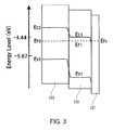
- Fig. 3 is a conceptual diagram indicating a band structure of the conductor, the first semiconductor layer and the second semiconductor layer, after being joined, which constitute the semiconductor electrode in the photoelectrochemical cell of the present embodiment.
- the vertical axis indicates energy levels relative to the vacuum level (unit: eV).
- eV vacuum level
- a photoelectrochemical cell 100 of the present embodiment includes a semiconductor electrode 120, a counter electrode 130, an electrolyte 140, and a container 110.
- the counter electrode 130 is an electrode paired with the semiconductor electrode 120.
- the electrolyte 140 contains water.
- the container 110 accommodates the semiconductor electrode 120, the counter electrode 130 and the electrolyte 140, and has an opening.
- the semiconductor electrode 120 and the counter electrode 130 are disposed inside the container 110 so that the surfaces thereof are in contact with the electrolyte 140.
- the semiconductor electrode 120 includes a conductor 121, a first semiconductor layer 122 disposed on the conductor 121 and a second semiconductor layer 123 disposed on the first semiconductor layer 122. That is, the semiconductor electrode 120 in the present embodiment is a semiconductor electrode in which the first to Nth (N is an integer of 2 or more) semiconductor layers are formed on the conductor 121, and in this case, N is 2.
- a semiconductor layer that constitutes the semiconductor electrode 120 includes the first semiconductor layer 122 and the second semiconductor layer 123 that are disposed in this order on the conductor 121.
- a portion of the container 110 facing the second semiconductor layer 123 of the semiconductor electrode 120 that is disposed inside the container 110 (which is, hereinafter, abbreviated as a light incident portion 110a) is made of a material that transmits light, such as sunlight.
- the conductor 121 of the semiconductor electrode 120 is connected electrically to the counter electrode 130 by a conducting wire 150.
- the counter electrode means an electrode that can exchange electrons with a semiconductor electrode without the intermediation of an electrolyte. Accordingly, the counter electrode 130 in the present embodiment only have to be connected electrically to the conductor 121 that constitutes the semiconductor electrode 120. There is no limitation on the positional relationship and the like of the counter electrode 130 with the semiconductor electrode 120,
- the first semiconductor layer 122 and the second semiconductor layer 123 satisfy the following relationships, relative to the vacuum level: E C 2 ⁇ E F 2 > E C 1 ⁇ E F 1 ; E F 2 ⁇ E V 2 ⁇ E F 1 ⁇ E V 1 ; E C 1 > ⁇ 4.44 eV ; E V 2 ⁇ ⁇ 5.67 eV ; ⁇ 5.67 eV ⁇ E F 1 ⁇ ⁇ 4.44 eV ; and ⁇ 5.67 eV ⁇ E F 2 ⁇ ⁇ 4.44 eV
- E C1 is the band edge level of the conduction band of the first semiconductor layer 122
- E V1 is the band edge level of the valence band of the first semiconductor layer 122
- E F1 is the Fermi level of the first semiconductor layer 122
- E C2 is the band edge level of the conduction band of the second semiconductor layer 123
- E V2 is the band edge level of the valence band of the second semiconductor layer 123
- E F2 is the Fermi level
- the semiconductor electrode 120 is set to satisfy the following (1) and (2):
- the semiconductor electrode 120 of the present embodiment is set to satisfy the following (I) and (II), relative to the vacuum level:
- the semiconductor electrode 120 of the present embodiment is set to satisfy the following (i) to (iv), relative to the vacuum level:
- a common material used as the conductor 121 has a higher Fermi level than the band edge level of its conduction band. Therefore, the difference value between the band edge level of the conduction band of the conductor 121 and the Fermi level thereof (the band edge level of the conduction band - the Fermi level) is a negative value. That is, the above difference value in the conductor 121 is greater than that in the first semiconductor layer 122. Therefore, electrons transfer smoothly from the first semiconductor layer 122 to the conductor 121, as is the case with the transfer from the second semiconductor layer 123 to the first semiconductor layer 122. As a result, the hydrogen production efficiency is further improved.
- the Fermi level E Fc of the conductor 121 is higher than the band edge level E C1 of the conduction band of the first semiconductor layer 122, and higher than -4.44 eV.
- a level "higher than -4.44 eV" relative to the vacuum level is equivalent to a level “lower than 0V” relative to the standard hydrogen electrode potential. Therefore, the Fermi level of the conductor 121 is lower than 0V, which is the reduction potential of water.
- hydrogen ions are reduced efficiently on the surface of the counter electrode 130 that is connected electrically to the conductor 121, so that hydrogen is generated efficiently.
- the band edge level E V2 of the valence band of the second semiconductor layer 123 that is disposed in contact with the electrolyte 140 is lower than -5.67 eV.
- a level “lower than -5.67 eV” relative to the vacuum level is equivalent to a level “higher than 1.23 V” relative to the standard hydrogen electrode potential. Therefore, the band edge level E V2 of the valence band of the second semiconductor layer 123 is higher than 1.23 V, which is the oxidation potential of water. As a result, water is oxidized efficiently on the surface of the second semiconductor layer 123, so that oxygen is generated efficiently.
- the Fermi levels E F1 and E F2 be set to satisfy -5.67 eV ⁇ E F1 ⁇ -4.44 eV and -5.67 eV ⁇ E F2 ⁇ -4.44 eV, respectively, relative to the vacuum level.
- the device can generate hydrogen using water in the form of almost fresh water.
- the conductor 121, the first semiconductor layer 122 and the second semiconductor 123 are joined to one another.
- carriers transfer so that the Fermi levels of these layers coincide, as indicated in Fig. 3 . This results in bending of the band edge.
- the band edge level E C2 of the conduction band, the band edge level E V2 of the valence band, and the Fermi level E F2 of the second semiconductor layer 123 and the band edge level E C1 of the conduction band, the band edge level E V1 of the valence band, and the Fermi level E F1 of the first semiconductor layer 122 satisfy the relationships of E C2 - E F2 > E C1 - E F1 and E F2 - E V2 ⁇ E F1 - E V1 , relative to the vacuum level. Therefore, no Schottky barrier is formed at the junction plane between the first semiconductor layer 122 and the second semiconductor layer 123.
- the Fermi level E F2 of the second semiconductor layer 123, the Fermi level E F1 of the first semiconductor layer 122, the Fermi level E Fc of the conductor 121, and the Fermi level E Fs of the electrolyte 140 be set to satisfy E Fs > E Fc ⁇ E F1 ⁇ E F2 . Therefore, no Schottky barrier is formed at the junction planes between the first semiconductor layer 122, the second semiconductor layer 123, the conductor 121, and the electrolyte 140. As a result, higher hydrogen production efficiency is achieved.
- the Fermi level E Fc of the conductor 121 is set higher than the Fermi level E F1 of the first semiconductor layer 122, relative to the vacuum level. Therefore, the junction between the conductor 121 and the first semiconductor layer 122 is an ohmic contact.
- the Fermi level E Fc of the conductor 121 is set higher than the Fermi level E F1 of the first semiconductor layer 122 in order to generate hydrogen more efficiently.
- it is not limited to this. Even if the Fermi level E Fc of the conductor 121 is lower than the Fermi level E F1 of the first semiconductor layer 122, it is possible to generate hydrogen.
- the Fermi level E Fs of the electrolyte 140 satisfies the relationship of E Fs ⁇ E Fc ⁇ E F1 ⁇ E F2 . However, even if this relationship is not satisfied, it is possible to generate hydrogen.
- the band edge level E C2 of the conduction band and the band edge level E V2 of the valence band around the surface of the second semiconductor layer 123 are raised at the interface between the second semiconductor layer 123 and the electrolyte 140.
- a space charge layer is formed around the surface of the second semiconductor layer 123.
- the difference value between the band edge level of the conduction band of the second semiconductor layer 123 and the Fermi level of the second semiconductor layer 123 is set greater than that in the first semiconductor layer 122. Accordingly, no square well potential as mentioned above occurs in the band edge level of the conduction band inside the second semiconductor layer 123. Therefore, the electrons are not accumulated inside the second semiconductor layer 123 and can transfer toward the side of the first semiconductor layer 122. As a result, the efficiency of charge separation is improved significantly.
- the difference value between the Fermi level of the first semiconductor layer 122 and the band edge level of the valence band of the first semiconductor layer 122 is set greater than that in the second semiconductor layer 123. Accordingly, no square well potential as mentioned above occurs in the band edge level of the valence band inside the second semiconductor layer 223. Therefore, the holes are not accumulated inside the second semiconductor layer 123 and can transfer toward the interface direction with the electrolyte. As a result, the efficiency of charge separation is improved significantly.
- the photoelectrochemical cell 100 of the present embodiment causes band bending but forms no Schottky barrier at the interface between the first semiconductor layer 122 and the second semiconductor layer 123.
- the electrons transfer to the conduction band of the first semiconductor layer 122, and the holes transfer in the valence band toward the interface direction with the electrolyte. Therefore, an efficient charge separation between the electrons and holes is achieved without being blocked by Schottky barriers. This reduces the probability of the recombination between the electrons and holes generated by photoexcitation inside the second semiconductor layer 123. As a result, the quantum efficiency of the hydrogen evolution reaction by irradiation with light is improved.
- the Fermi level of the conductor 121 is set higher than the Fermi level of the first semiconductor layer 122.
- This configuration forms no Schottky barrier also at the junction plane between the conductor 121 and the first semiconductor layer 122. Therefore, the electrons can transfer from the first semiconductor layer 122 to the conductor 121 without being blocked by Schottky barriers. This further reduces the probability of the recombination between the electrons and holes generated by photoexcitation inside the second semiconductor layer 123. As a result, the quantum efficiency of the hydrogen evolution reaction by irradiation with light is further improved.
- the Fermi level, the potential (band edge level) at the bottom of the conduction band, and the potential (band edge level) at the top of the valence band of each of the first semiconductor layer 122 and the second semiconductor layer 123 can be calculated using the flat band potential and carrier concentration.
- the flat band potential and carrier concentration of a semiconductor can be determined from a Mott-Schottky plot obtained by measurement using, as an electrode, the semiconductor to be measured. These energy levels can also be determined physically by ultraviolet photoelectron spectroscopy (UPS) or by measurement using an atmospheric photoelectron spectrometer (AC-3, Riken Keiki Co., Ltd.).
- the potential (band edge level) at the top of the valence band of each of the first semiconductor layer 122 and the second semiconductor layer 123 can be calculated using the band gap and the potential at the bottom of the conduction band of each of the semiconductor layer 122 and the second semiconductor layer 123 calculated by the above-mentioned method.
- the band gap of each of the semiconductor layer 122 and the second semiconductor layer 123 can be obtained from the optical absorption edge observed in the measurement of the light absorption spectrum of the semiconductor to be measured.
- the Fermi level of the conductor 121 can be determined, for example, by photoelectron spectroscopy.
- the materials of the first semiconductor layer 122 and the second semiconductor layer 123 in the present embodiment are described. In the present embodiment, however, the case where n-type semiconductors are used is described.
- N-type semiconductors whose band structures satisfy the above-described relationships can be selected for the first semiconductor layer 122 and the second semiconductor 123 layer. Therefore, there is no limitation on the materials for the first semiconductor layer 122 and the second semiconductor layer 123. Preferably, one selected from the group consisting of oxide, nitride and oxynitride is used as the n-type semiconductors for the first semiconductor layer 122 and the second semiconductor layer 123. With the use of these materials, the first semiconductor layer 122 and the second semiconductor layer 123 are prevented from dissolving in the electrolyte 140, in a state where the semiconductor electrode 120 is in contact with the electrolyte 140. Accordingly, the photoelectrochemical cell can operate stably.
- the junction between the conductor 121 of the semiconductor electrode 120 and the first semiconductor layer 122 is an ohmic contact.
- electrically conductive materials such as ITO (Indium Tin Oxide) and FTO (Fluorine-doped Tin Oxide), or metals such as Ti, Ni, Ta, Nb, A1 and Ag, can be used, for example.
- the conductor 121 it is preferable that, in the surface of the conductor 121, the area that is not covered by the first semiconductor layer 122 be coated, for example, with an insulating material such as a resin. With such a configuration, the conductor 121 can be prevented from dissolving in the electrolyte 140.
- a material with a low overvoltage is used preferably for the counter electrode 130.
- hydrogen is generated at the counter electrode 130. Therefore, Pt, Au, Ag, Fe, or the like is used preferably as the counter electrode 130, for example.
- electrolyte containing water can be used for the electrolyte 140.
- the electrolyte containing water may be acidic or alkali.
- the electrolyte 140 in contact with the surface of the second semiconductor layer 123 of the semiconductor electrode 120 and the surface of the counter electrode 130 can be replaced by pure water for electrolysis.
- oxides, chalcogenides, sulfides, nitrides, oxynitrides, phosphides, and the like, containing barium, strontium, calcium, zirconium, titanium, cerium, gadolinium, gallium, indium, yttrium, ytterbium, and/or scandium, as constituent elements, can be used for the first semiconductor layer 122 and the second semiconductor layer 123.
- an oxide containing barium, zirconium, and indium, as constituent elements is used preferably.
- the use of such an oxide allows the Fermi level E F1 of the first semiconductor layer 122 to be set higher than -5.67 eV but lower than -4.44 eV, relative to the vacuum level. That is, the Fermi level of the first semiconductor layer 122 can be set higher than 0V but lower than 1.23 V, relative to the standard hydrogen electrode potential.
- the first semiconductor layer 122 may be an oxide of barium, zirconium and indium, a composite oxide thereof, or a mixture of such oxide and composite oxide.
- the first semiconductor layer 122 may be the above-mentioned compound additionally containing metal ions other than indium ions.
- An oxide containing barium, zirconium, cerium, and indium, as constituent elements, also can be used suitably.
- the p-type semiconductor may contain at least one selected from perovskite-type oxide semiconductors represented by the following general formulae A and B: BaZr 1 - x M x O 3 - ⁇ (General Formula A) where M denotes at least one element selected from trivalent elements, x denotes a numerical value of more than 0 and less than 1 (preferably less than 0.5), and ⁇ denotes an amount of oxygen deficiency that is a numerical value of more than 0 and less than 1.5; and BaZr x Ce y M 1-x-y O 3- ⁇ (General Formula B) where M denotes at least one element selected from trivalent elements, x denotes a numerical value of more than 0 and less than 1, y denotes a numerical value of more than 0 and less than 1, x + y ⁇ 1 is satisfied, and ⁇ denotes an amount of oxygen deficiency that is a numerical value of more than 0 and less than 1.5.
- M denotes at least one element selected from trivalent elements
- An oxide containing barium, zirconium and indium as constituent elements or an oxide containing barium, zirconium, cerium and indium as constituent elements are also used suitably for the second semiconductor layer 123, as is the case with the first semiconductor layer 122.
- a material containing at least one selected from semiconductors represented by the above general formula A and general formula B also can be used.
- the carrier concentration of the p-type semiconductor in the second semiconductor layer 123 preferably is lower than the carrier concentration of the p-type semiconductor in the first semiconductor layer 122.
- the p-type semiconductor in the second semiconductor layer 123 preferably is one selected from the group consisting of oxide, nitride and oxynitride.
- the second semiconductor layer 123 is prevented from dissolving in the electrolyte 140, even if the second semiconductor layer 123 is irradiated with light in a state where the semiconductor electrode 120 is in contact with the electrolyte 140. Accordingly, the photoelectrochemical cell can operate stably.
- an oxide containing barium, zirconium and indium as constituent elements is used as a p-type semiconductor for the first semiconductor layer 123
- an oxide containing, for example, barium, zirconium, cerium and indium as constituent elements can be used as a p-type semiconductor for the second semiconductor layer 123.
- preferable examples of p-type semiconductors used to form a semiconductor layer include BaZr 0.95 In 0.05 O 3 - ⁇ , BaZr 0.9 In 0.1 O 3- ⁇ , BaZr 0.875 In 0.125 O 3- ⁇ , BaZr 0.85 In 0.15 O 3- ⁇ , BaZr 0.8 In 0.2 O 3- ⁇ , BaZr 0.75 In 0.25 O 3- ⁇ , BaZr 0.8 Ga 0.2 O 3- ⁇ , BaZr 0.9 Ga 0.1 O 3- ⁇ , BaZr 0.8 Gd 0.2 O 3- ⁇ , BaZr 0.9 Gd 0.1 O 3- ⁇ , BaZr 0.8 Y 0.2 O 3- ⁇ , BaZr 0.4 Ce 0.4 In 0.2 O 3- ⁇ , and BaZr 0.6 Ce 0.2 In 0.2 O 3- ⁇ .
- Table 1 shows the band edge levels (E) of the conduction bands, the band edge levels (Ev) of the valence bands, and the Fermi levels (E F ) of these p-type semiconductors.
- Table 1 also shows the difference values (E C - EF) between the band edge levels of the conduction bands and the Fermi levels and the difference values (E F - Ev) between the band edge levels of the valence bands and the Fermi levels.
- the semiconductor layer provided on the conductor includes the first semiconductor layer and the second semiconductor layer (i.e., a configuration in which two semiconductor layers are provided on the conductor) is shown in the present embodiment.
- the configuration of the photoelectrochemical cell of the present invention is not limited to this.
- the semiconductor layer provided on the conductor may include the first to Nth (N is an integer of 2 or more) semiconductor layers that are disposed in this order on the conductor. Therefore, it also is possible to use a semiconductor electrode in which three or more semiconductor layers are provided on a conductor.
- the (K-1)th semiconductor layer and the Kth semiconductor layer can be set to satisfy the following relationships, relative to the vacuum level: E CK ⁇ E FK > E C K ⁇ 1 ⁇ E F K ⁇ 1 ; E FK ⁇ E VK ⁇ E F K ⁇ 1 ⁇ E V K ⁇ 1 ; E C K ⁇ 1 > ⁇ 4.44 eV ; E VK ⁇ ⁇ 5.67 eV ; ⁇ 5.67 eV ⁇ E F K ⁇ 1 ⁇ ⁇ 4.44 eV ; and ⁇ 5.67 eV ⁇ E FK ⁇ ⁇ 4.44 eV
- E C(K-1) is the band edge level of the conduction band of the (K-1)th semiconductor layer
- E V(K-1) is the band edge level of the valence band in the (K-1)th semiconductor layer
- E F(K-1) is the Fermi level of the (K-1)th semiconductor layer
- E CK is the band edge level of the conduction band of the K
- the semiconductor electrode may include a conductor and one semiconductor layer disposed on the conductor.
- a configuration in which the semiconductor layer includes at least two elements and at least one of the elements in the semiconductor layer has a concentration increasing or decreasing along the thickness direction of the semiconductor layer, can be adopted.
- Such a state of the semiconductor layer can be expressed in such a way that the composition is in a gradient.
- the surface near-field region of the semiconductor layer and the junction plane near-field region of the semiconductor layer with the conductor can be set to satisfy the following relationships, relative to the vacuum level: E CS ⁇ E FS > E CJ ⁇ E FJ ; E FS ⁇ E VS ⁇ E FJ ⁇ E VJ ; E CJ > ⁇ 4.44 eV ; E VS ⁇ ⁇ 5.67 eV ; ⁇ 5.67 eV ⁇ E FJ ⁇ ⁇ 4.44 eV ; and ⁇ 5.67 eV ⁇ E FS ⁇ ⁇ 4.44 eV
- E CJ is the band edge level of the conduction band in the junction plane near-field region of the semiconductor layer with the conductor
- E VJ is the band edge level of the valence band in the junction plane near-field region of the semiconductor layer with the conductor
- E FJ is the Fermi level in the junction plane near-field region of the semiconductor layer with the conductor
- E CS is the band edge level of the
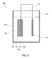
- Fig. 4 is a schematic view illustrating the configuration of the photoelectrochemical cell of the present embodiment.
- a semiconductor electrode 220 includes a conductor 221, a first semiconductor layer 222 disposed on the conductor 221, and a second semiconductor layer 223 disposed on the first semiconductor layer 222.
- the semiconductor electrode 220 further includes an insulation layer 224 disposed on the surface of the conductor 221 opposite to the surface on which the first semiconductor layer 222 is disposed.
- the conductor 221, the first semiconductor layer 222 and the second semiconductor layer 223, respectively, have the same structures as those of the conductor 121, the first semiconductor layer 122 and the second semiconductor layer 123 in Embodiment 1.
- the insulation layer 224 is formed, for example, of resin or glass.
- This insulation layer 224 can prevent the conductor 221 from dissolving in the electrolyte 140.
- a configuration in which an insulation layer as mentioned above is additionally provided on a semiconductor electrode including two semiconductor layers as shown in Embodiment 1 is adopted.
- Such an insulation layer can be employed also for each of the semiconductor electrodes described in Embodiment 1, one including three or more semiconductor layers and the other including a semiconductor layer with a gradient composition.
- Fig. 5 is a schematic view illustrating the configuration of the photoelectrochemical cell of the present embodiment.
- a semiconductor electrode 320 includes a conductor 321, a first semiconductor layer 322 disposed on the conductor 321 and a second semiconductor layer 323 disposed on the first semiconductor layer 322.
- a counter electrode 330 is disposed on the conductor 321 (on the surface of the conductor 321 opposite to the surface on which the first semiconductor layer 322 is disposed).
- the conductor 321, the first semiconductor layer 322 and the second semiconductor layer 323, respectively, have the same structures as those of the conductor 121, the first semiconductor layer 122 and the second semiconductor layer 123 in Embodiment 1.
- the configuration in which the counter electrode 330 is disposed on the conductor 321 can eliminate the need for a conducting wire for connecting the semiconductor electrode 320 electrically to the counter electrode 330. This can eliminate the ohmic loss derived from the conducting wire, therefore further improving the quantum efficiency of the hydrogen evolution reaction by irradiation with light. Furthermore, with such a configuration, the semiconductor electrode 320 can be connected electrically to the counter electrode 330 by a simple and easy process.
- the present embodiment shows a configuration in which the counter electrode 330 is disposed on the surface of the conductor 321 opposite to the surface on which the first semiconductor layer 322 is disposed.
- the counter electrode 330 is not limited to this configuration, and the counter electrode 330 can be disposed also on the same surface on which the first semiconductor layer 322 is disposed.
- the above configuration in which a counter electrode is disposed on a conductor in a photoelectrochemical cell including two semiconductor layers as shown in Embodiment 1 is adopted.
- Such a configuration can be employed also for each of the semiconductor electrodes described in Embodiment 1, one including three or more semiconductor layers and the other including a semiconductor layer with a gradient composition.
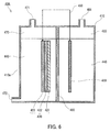
- Fig. 6 is a schematic view illustrating the configuration of the photoelectrochemical cell of the present embodiment.
- a photoelectrochemical cell 400 of the present embodiment includes a housing (container) 410, a semiconductor electrode 420, a counter electrode 430 and a separator 460.
- the separator 460 separates the inside of the housing 410 into two chambers: a first chamber 470 and a second chamber 480.
- An electrolyte 440 containing water is contained in each of the first chamber 470 and the second chamber 480.
- the semiconductor electrode 420 is disposed at a position in contact with the electrolyte 440 inside the first chamber 470.
- the semiconductor electrode 420 includes a conductor 421, a first semiconductor layer 422 disposed on the conductor 421 and a second semiconductor layer 423 disposed on the first semiconductor layer 422.
- the first chamber 470 includes a first gas outlet 471 for discharging oxygen generated inside the first chamber 470 and a water inlet 472 for supplying water into the first chamber 470.
- a portion of the housing 410 that faces the second semiconductor layer 423 of the semiconductor electrode 420 disposed inside the first chamber 470 (hereinafter, abbreviated as a light incident portion 410a) is made of a material that transmits light such as sunlight.
- the counter electrode 430 is disposed inside the second chamber 480 at a position in contact with the electrolyte 440.
- the second chamber 480 includes a second gas outlet 481 for discharging hydrogen generated inside the second chamber 480.
- the conductor 421 of the semiconductor electrode 420 is connected electrically to the counter electrode 430 by a conducting wire 450.
- the conductor 421, the first semiconductor layer 422 and the second semiconductor layer 423 of the semiconductor electrode 420 in the present embodiment, respectively, have the same structures as those of the conductor 121, the first semiconductor layer 122 and the second semiconductor layer 123 of the semiconductor electrode 120 in Embodiment 1. Accordingly, the semiconductor electrode 420 has the same operational effects as those of the semiconductor electrode 120 of Embodiment 1. Furthermore, the counter electrode 430 and the electrolyte 440 respectively are the same as the counter electrode 130 and the electrolyte 140 in Embodiment 1.
- the separator 460 is formed of a material that allows the electrolyte 440 to permeate itself and has a function of blocking gas generated inside each of the first chamber 470 and the second chamber 480.
- the material of the separator 460 include a solid electrolyte such as a solid polymer electrolyte.
- a solid polymer electrolyte As the solid polymer electrolyte, an ion exchange membrane such as Nafion (registered trademark) can be mentioned, for example.
- the electrolyte and the surface of the semiconductor electrode i.e., the semiconductor layer
- the electrolyte and the surface of the semiconductor electrode are made in contact in one of the areas while the electrolyte and the surface of the counter electrode are made in contact in the other area. With such a configuration, oxygen and hydrogen generated inside the container can be separated easily.
- the photoelectrochemical cell 400 using the semiconductor electrode 420 having the same structure as that of the semiconductor electrode 120 in Embodiment 1 is described in the present embodiment.
- a semiconductor electrode including three or more semiconductor layers or a semiconductor electrode including a semiconductor layer with a gradient composition described also in Embodiment 1, instead of the semiconductor electrode 420.
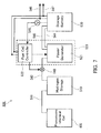
- Fig. 7 is a schematic view illustrating the configuration of the energy system of the present embodiment.
- an energy system 500 of the present embodiment includes the photoelectrochemical cell 400, a hydrogen storage 510, a fuel cell 520 and a storage battery 530.
- the photoelectrochemical cell 400 is the photoelectrochemical cell described in Embodiment 4 and the specific configuration thereof is as illustrated in Fig. 6 . Therefore, detailed descriptions thereof are omitted.
- the hydrogen storage 510 is connected to the second chamber 480 (see Fig. 6 ) of the photoelectrochemical cell 400 by a first pipe 541.
- the hydrogen storage 510 can be constituted, for example, by a compressor for compressing the hydrogen generated in the photoelectrochemical cell 400 and a high-pressure hydrogen tank for storing the hydrogen compressed by the compressor.
- the fuel cell 520 includes a power generator 521 and a fuel cell controller 522 for controlling the power generator 521.
- the fuel cell 520 is connected to the hydrogen storage 510 by a second pipe 542.
- the second pipe 542 is provided with a shutoff valve 543.
- a solid polymer electrolyte fuel cell can be used as the fuel cell 520.
- the positive electrode and the negative electrode of the storage battery 530 respectively are connected electrically to the positive electrode and the negative electrode of the power generator 521 in the fuel cell 520 by a first line 544 and a second line 545.
- the storage battery 530 is provided with a capacity meter 546 for measuring the remaining capacity of the storage battery 530.
- a lithium ion battery can be used as the storage battery 530, for example.
- the electrons transfer toward the conductor 421 along the bending of the band edge of the conduction band at the interface between the second semiconductor layer 423 and the first semiconductor layer 422 and at the interface between the first semiconductor layer 422 and the conductor 421.
- the electrons that have transferred to the conductor 421 transfer toward the side of the counter electrode 430 connected electrically to the conductor 421 through the conducting wire 450.
- hydrogen is generated on the surface of the counter electrode 430 according to the above reaction formula (2).
- Oxygen generated inside the first chamber 470 is discharged from the first gas outlet 471 to the outside of the photoelectrochemical cell 400.
- hydrogen generated inside the second chamber 480 is supplied into the hydrogen storage 510 through the second gas outlet 481 and the first pipe 541.
- the shutoff valve 543 is opened according to signals from the fuel cell controller 522, so that the hydrogen stored inside the hydrogen storage 510 is supplied to the power generator 521 of the fuel cell 520 through the second pipe 542.
- the electricity generated in the power generator 521 of the fuel cell 520 is stored inside the storage battery 530 through the first line 544 and the second line 545.
- the electricity stored inside the storage battery 530 is supplied to households, enterprises, and the like through a third line 547 and a fourth line 548.
- the photoelectrochemical cell 400 it is possible to improve the quantum efficiency of the hydrogen evolution reaction by irradiation with light.
- the energy system 500 of the present embodiment provided with this photoelectrochemical cell 400 can provide an efficient power supply.
- an energy system using the photoelectrochemical cell 400 described in Embodiment 4 is exemplified.
- the same effects can be obtained also when the photoelectrochemical cells 100, 200 and 300 described in Embodiments 1 to 3 each are used.
- Example 1 a photoelectrochemical cell having the same configuration as that of the photoelectrochemical cell 200 indicated in Fig. 4 was produced.
- the photoelectrochemical cell of Example 1 is described below with reference to Fig. 4 .
- the photoelectrochemical cell 200 of Example 1 was provided with a rectangular glass container (container 110) with an opening in the upper part, the semiconductor electrode 220 and the counter electrode 130.
- the glass container 110 held therein 0.01 mol/L Na 2 SO 3 aqueous solution containing 0.01 mol/L Na 2 S as the electrolyte 140.
- the semiconductor electrode 220 was produced according to the following procedure.
- a 150 nm-thick ITO film (sheet resistance 10 ⁇ /sq.) as the conductor 221 was formed by sputtering on a 1 cm-square glass substrate as the insulation layer 224.
- a 300 nm-thick BaZr 0.8 In 0.2 O 3- ⁇ film as the first semiconductor layer 222 was formed by electrodeposition on the conductor 221.
- a 1 ⁇ m-thick BaZr 0.9 In 0.1 O 3- ⁇ film as the second semiconductor layer 223 was formed also by electrodeposition on the first semiconductor layer 222.
- the semiconductor electrode 220 was disposed so that the surface of the second semiconductor layer 223 faced the light incident surface 110a of the glass container 110.
- a platinum plate was used as the counter electrode 130.
- a portion of the conductor 221 of the semiconductor electrode 220 was connected electrically to the counter electrode 130 by the conducting wire 150. The current flowing between the semiconductor electrode 220 and the counter electrode 130 was measured with an ammeter.
- the first semiconductor layer 222 was not provided on the conductor 221 but a BaZr 0.9 In 0.1 O 3- ⁇ film as the second semiconductor layer 223 was provided thereon in the semiconductor electrode 220 of Example 1. Except for this point, a photoelectrochemical cell of Comparative Example 1 was produced by the same procedure as used for the photoelectrochemical cell 200 of Example 1.
- a ⁇ m-thick Cu 2 O film was provided as the second semiconductor layer 223 instead of the BaZ 0.9 In 0.1 O 3- ⁇ film in the semiconductor electrode 220 of Example 1. Except for this point, a photoelectrochemical cell of Comparative Example 3 was produced by the same procedure as used in Example 1.
- Example 2 a photoelectrochemical cell having the same configuration as that of the photoelectrochemical cell 100 indicated in Fig. 1 was produced.
- the photoelectrochemical cell of Example 2 is described below with reference to Fig. 1 .
- the photoelectrochemical cell 100 of the present example a Ti substrate was used as the conductor 121.
- the photoelectrochemical cell 100 of the present example is different from the photoelectrochemical cell 200 of Example 1 in that a 500 nm-thick BaZr 0.8 In 0.2 O 3- ⁇ film as the first semiconductor layer 122 was formed by electrodeposition on the conductor 121, a glass substrate as an insulation layer was not provided on the back surface of the conductor 121, and the back surface of the conductor 121 was coated with fluororesin. Since the configuration of the photoelectrochemical cell 100 of the present example is the same as that of the photoelectrochemical cell 200 of Example 1 except for these differences, the description thereof is omitted.
- Example 3 a photoelectrochemical cell having the same configuration as that of the photoelectrochemical cell 300 indicated in Fig. 5 was produced.
- the photoelectrochemical cell of Example 3 is described below with reference to Fig. 5 .
- the semiconductor electrode 320 and the counter electrode 330 were produced according to the following procedure.
- the conductor 32 As the conductor 321, a 1 cm-square Ti substrate was used. A 500 nm-thick BaZr 0.4 Ce 0.4 In 0.2 O 3- ⁇ film as the first semiconductor layer 322 was formed by electrodeposition on this Ti substrate. Next, a 1 ⁇ m-thick BaZ 0.9 In 0.1 O 3- ⁇ film as the second semiconductor layer 323 was formed by electrodeposition on the first semiconductor layer 322, in the same manner as in Example 1. Finally, a 10 nm-thick Pt film as the counter electrode 330 was formed by sputtering on the back surface of the Ti substrate as the conductor 321. The semiconductor electrode 320 was disposed so that the surface of the second semiconductor layer 323 faced the light incident surface 110a of the glass container 110.
- Example 4 a photoelectrochemical cell including a semiconductor electrode in which first to third semiconductor layers were provided in this order on a conductor was produced.
- the photoelectrochemical cell of Example 4 has a configuration in which the third semiconductor layer is additionally provided on the second semiconductor layer 223 in the semiconductor electrode 220 of the photoelectrochemical cell 200 indicated in Fig. 4 .
- the photoelectrochemical cell of Example 4 is described below with reference to Fig. 4 .
- a 150 nm-thick ITO film (sheet resistance 10 ⁇ /sq.) as the conductor 221 was formed by sputtering on a 1 cm-square glass substrate as the insulation layer 224.
- a 300 nm-thick BaZr 0.8 In 0.2 O 3- ⁇ film as the first semiconductor layer 222 was formed by electrodeposition on the conductor 221.
- a 500 nm-thick BaZr 0.9 In 0.1 O 3- ⁇ film as the second semiconductor layer 223 was formed also by electrodeposition on the first semiconductor layer 222.
- a 1 ⁇ m-thick BaZr 0.95 In 0.05 O 3- ⁇ film as the third semiconductor layer was formed also by electrodeposition on the second semiconductor layer 223.
- the semiconductor electrode 220 was disposed so that the surface of the third semiconductor layer faced the light incident surface 110a of the glass container 110.
- a photoelectrochemical cell of Comparative example 4 was produced by the same procedure as used in Example 1, except that the materials of the first semiconductor layer 222 and the second semiconductor layer 223 were replaced by n-type semiconductors in the semiconductor electrode 220 of Example 1.
- the first semiconductor layer 222 a 300 nm-thick TiO2 film was formed by electrodeposition.
- the band edge level of the conduction band of titanium oxide was -4.24 eV
- the band edge level of the valence band thereof was -7.44 eV
- the Fermi level thereof was -4.84 eV
- the band edge level of the conduction band of CdS was -4.04 eV
- the band edge level of the valence band thereof was -6.54 eV
- the Fermi level thereof was -5.24 eV
- Tables 2 and 3 below indicate the materials, the Fermi levels (unit: eV), the band edge levels (unit: eV) of the conduction bands, and the band edge levels (unit: eV) of the valence bands of the conductor, the p-type semiconductor and n-type semiconductor used for the production of the semiconductor electrode in each of the photoelectrochemical cells of Examples 1 to 5 and Comparative Examples 1 to 3. It should be noted that the Fermi levels of the semiconductors indicated herein are the values relative to the vacuum level.
- the Fermi levels of the semiconductors are considered to be pulled down to the same level as the Fermi level of the electrolyte at a pH of 7 and a temperature of 25°C by that Fermi level of the electrolyte.
- the band edge level of the conduction band and the band edge level of the valence band of the second semiconductor layer, respectively, were higher than the band edge level of the conduction band and the band edge level of the valence band of the first semiconductor layer.
- the Fermi level of the first semiconductor layer was the same as that of the second semiconductor layer. Therefore, a value obtained by subtracting the Fermi level of the second semiconductor layer from the band edge level of the conduction band of the second semiconductor layer was greater than that in the first semiconductor layer. Furthermore, a value obtained by subtracting the band edge level of the conduction band of the second semiconductor layer from the Fermi level of the second semiconductor layer was smaller than that in the first semiconductor layer.
- the Fermi levels of the semiconductors used in Examples 1 to 3 were -5.08 eV, which was within the range of -5.67 eV to -4.44 eV.
- the band edge levels of the conduction bands of the first semiconductor layers were higher than -4.44 eV.
- the band edge levels of the valence bands of the second semiconductor layers were lower than -5.67 eV. Therefore, the photoelectrochemical cells of Examples 1 to 3 met the structural requirements of the semiconductor electrode of the present invention.
- the semiconductor electrode in the photoelectrochemical cell of Example 4 included the first to third semiconductor layers.
- n-type semiconductors were used for the first semiconductor layer and the second semiconductor layer.
- the band edge level of the conduction band and the band edge level of the valence band of the second semiconductor layer, respectively, were higher than the band edge level of the conduction band and the band edge level of the valence band of the first semiconductor layer.
- the Fermi level of the first semiconductor layer was higher than that of the second semiconductor layer. Therefore, a value obtained by subtracting the Fermi level of the second semiconductor layer from the band edge level of the conduction band of the second semiconductor layer was greater than that in the first semiconductor layer.
- a value obtained by subtracting the band edge level of the conduction band of the second semiconductor layer from the Fermi level of the second semiconductor layer was smaller than that in the first semiconductor layer.
- the Fermi level of the first semiconductor layer and the Fermi level of the second semiconductor layer used in Comparative example 4 were -4.84 eV and -5.24 eV, respectively, which were within the range of -5.67 eV to -4.44 eV
- the band edge level of the conduction band of the first semiconductor layer was higher than -4.44 eV, and the band edge level of the valence band of the second semiconductor layer was lower than -5.67 eV Therefore, the photoelectrochemical cell of Comparative example 4 met the energetic requirements of the semiconductor electrode of the present invention.
- the simulated sunlight irradiation experiment was conducted as follows.
- a solar simulator manufactured by SERIC Ltd. was used to apply simulated sunlight.
- the surface of the second semiconductor layer (or the third semiconductor layer) in the semiconductor electrode of each of the photoelectrochemical cells of Examples 1-4 and Comparative Examples 1-4 was irradiated with simulated sunlight at an intensity of 1 kW/m 2 through the light incident portion of each photoelectrochemical cell.
- the gas generated on the surface of the counter electrode was collected for 30 minutes.
- the components of the collected gas were analyzed and the amount of the gas generated was determined by gas chromatography.
- the density of the photocurrent flowing between the semiconductor electrode and the counter electrode was measured with an ammeter. The apparent quantum efficiency was calculated using the amount of the gas generated on the counter electrode.
- Table 4 below indicates the apparent quantum efficiency measured for each of the photoelectrochemical cells of Examples 1-4 and Comparative Examples 1-4 .
- the photoelectrochemical cell of Comparative Example 2 was irradiated with light. Although it was observed that gas was generated on the surface of the counter electrode, the amount of gas generated was too small to be detected.
- the Fermi level of the first semiconductor layer (p-type semiconductor layer) on the conductor side was lower than that of the second semiconductor layer (n-type semiconductor layer) on the surface side. Therefore, Schottky barriers were formed at the junction plane between the first semiconductor layer and the second semiconductor layer. Probably, these barriers prevented charge separation between the electrons and holes generated by photoexcitation inside the second semiconductor layer, resulting in a higher probability of the recombination between the generated electrons and holes, and thus, in a failure to generate hydrogen efficiently.
- Photoelectrochemical cells were produced with various combinations of the p-type semiconductor materials indicated in Table 1 so that the structural requirements of the semiconductor electrode of the present invention were met, and the apparent quantum efficiencies thereof were measured. As a result, the highest apparent quantum efficiency was 40%.
- BaZr 0.8 In 0.2 O 3- ⁇ was used for the first semiconductor layer in the photoelectrochemical cell of Example 2, and BaZr 0.8 In 0.2 O 3- ⁇ was used for the first semiconductor layer in the photoelectrochemical cell of Example 4, but instead, BaZr 0.4 Ce 0.4 In 0.2 O 3- ⁇ may be used.
- a BaZr 0.4 Ce 0.4 In 0.2 O 3- ⁇ film can be formed, for example, by sputtering.
- the band edge level of the conduction band and the band edge level of the valence band are indicated in Table 1.
- a semiconductor electrode using these materials also meets the requirements of the semiconductor electrode of the present invention. This means that the apparent quantum efficiency is expected to be improved, as is the case with Example 1.
- the band edge levels of the conduction bands and the band edge levels of the valence bands, and the band gaps of the p-type semiconductors indicated in Table 1 are the actual values measured by UPS, AC-3, or ultraviolet-visible spectroscopy (UV-Vis).
- UV-Vis ultraviolet-visible spectroscopy
- photoelectron spectroscopic measurement was performed in vacuum using a sample obtained by electrodepositing a powder sample on a Pt substrate.
- AC-3 photoelectron spectroscopic measurement with an atmospheric photoelectron spectrometer (AC-3, Riken Keiki Co., Ltd.) was performed in the atmosphere using a disk-shaped bulk sample (with a diameter of 12 cm and a thickness of 0.5 cm).
- UV-Vis absorption spectroscopic measurement was performed by a transmission method or a diffuse reflection method also using a disk-shaped bulk sample or a powder sample.
- the photoelectrochemical cell and the energy system of the present invention can improve the quantum efficiency of the hydrogen evolution reaction by irradiation with light, and thus are useful as a domestic power generation system and the like.
Description
- The present invention relates to a photoelectrochemical cell in which water is decomposed by irradiation with light and to an energy system using the photoelectro-chemical cell.
- There is a conventionally known technique for decomposing water by irradiating a semiconductor material that acts as a photocatalyst with light to obtain hydrogen and oxygen (see, for example,
JP 51(1976)-123779 A -
JP 51(1976)-123779 A JP 51(1976)-123779 A -
JP 2002-234105 A JP 2002-234105 A - There is also proposed a photocatalytic thin film that exhibits highly efficient photocatalytic performance under natural light (see
JP 2002-143688 A
the thickness direction. - Furthermore, there is also proposed a technique for producing hydrogen by irradiating a multilayer thin film photocatalyst with light (see
JP 2003-154272 A - However, the method described in
JP 51(1976)-123779 A -
JP 2002-234105 A JP 2002-234105 A JP 2002-234105 A - The photocatalyst thin film described in
JP 2002-143688 A JP 2002-143688 A - A multilayer thin film photocatalyst described in
JP 2003-154272 A JP 2003-154272 A JP 2003-154272 A - In view of such conventional problems, it is an object of the present invention to provide a photoelectrochemical cell capable of efficient charge separation between electrons and holes generated by photoexcitation and thus improving the quantum efficiency of the hydrogen evolution reaction by irradiation with light. It is a further object of the present invention to provide an energy system using such a photoelectrochemical cell.
- In order to achieve the above objects, the present invention provides a photoelectrochemical cell including: a semiconductor electrode including a conductor and a semi-conductor layer comprising a first semiconductor layer and a second semiconductor layer, the first semiconductor layer being disposed on the conductor and the second semiconductor layer being disposed on the first semiconductor layer; a counter electrode connected electrically to the conductor; an electrolyte in contact with surfaces of the second semiconductor layer and the counter electrode; and a container accommodating the semiconductor electrode, the counter electrode and the electrolyte. In this photoelectrochemical cell, a band edge level ECS of a conduction band, a band edge level EVS of a valence band, and a Fermi level EFS in the second semiconductor layer, and a band edge level ECJ of a conduction band, a band edge level EVJ of a valence band, and a Fermi level EFJ in the first semiconductor layer satisfy, relative to a vacuum level, ECS - EFS > ECJ - EFJ, EFS - EVS < EFJ - EVJ, ECJ > -4.44 eV, and EVS < -5.67 eV, and the Fermi level EFS in the second semiconductor layer and the Fermi level EFJ in the first semiconductor layer with the conductor satisfy, relative to the vacuum level, -5.67 eV < EFS < -4.44 eV and -5.67 eV < EFJ < -4.44 eV. The first semiconductor layer contains an oxide containing as constituent elements barium, zirconium and indium or barium, zirconium, cerium and indium, and the second semiconductor contains an oxide containing as constituent elements barium, zirconium and indium as constituent elements, or barium, zirconium, cerium and indium.
- The present invention further provides an energy system including: the photoelectrochemical cell of the present invention; a hydrogen storage, connected to the photoelectrochemical cell by a first pipe, for storing hydrogen generated inside the photoelectrochemical cell; and a fuel cell, connected to the hydrogen storage by a second pipe, for converting the hydrogen stored in the hydrogen storage into electricity.
- The photoelectrochemical cell of the present invention makes it possible to achieve efficient charge separation between electrons and holes generated by photoexcitation. Thus, the photoelectrochemical cell of the present invention makes it possible to improve the quantum efficiency of the hydrogen evolution reaction by irradiation with light. Since the energy system of the present invention is provided with such a photoelectrochemical cell, efficient power supply is achieved.
-
-
Fig. 1 is a schematic view illustrating a configuration of the photoelectrochemical cell of Embodiment 1 of the present invention. -
Fig. 2 is a conceptual diagram indicating a band structure of a conductor, a first semiconductor layer and a second semiconductor layer, before being joined, which constitute a semiconductor electrode in the photoelectrochemical cell of 35 Embodiment 1 of the present invention. -
Fig. 3 is a conceptual diagram indicating a band structure of the conductor, the first semiconductor layer and the second semiconductor layer, after being joined, which constitute the semiconductor electrode in the photoelectrochemical cell of Embodiment 1 of the present invention. -
Fig. 4 is a schematic view illustrating a configuration of the photoelectrochemical cell of Embodiment 2 of the present invention. -
Fig. 5 is a schematic view illustrating a configuration of the photoelectrochemical cell of Embodiment 3 of the present invention. -
Fig. 6 is a schematic view illustrating a configuration of the photoelectrochemical cell of Embodiment 4 of the present invention. -
Fig. 7 is a schematic view illustrating a configuration of the energy system of Embodiment 5 of the present invention. - Hereinafter, the embodiments of the present invention are described in detail with reference to the drawings. The embodiments described below are examples and the present invention is not limited to the following embodiments. Furthermore, in the following embodiments, the same members are indicated with identical numerals and the same descriptions thereof may be omitted.
- The configuration of the photoelectrochemical cell according to Embodiment 1 of the present invention is described with reference to
Fig. 1 to Fig. 3 .Fig. 1 is a schematic view illustrating the configuration of the photoelectrochemical cell of the present embodiment.Fig. 2 is a conceptual diagram indicating a band structure of a conductor, a first semiconductor layer and a second semiconductor layer, before being joined, which constitute a semiconductor electrode in the photoelectrochemical cell of the present embodiment.Fig. 3 is a conceptual diagram indicating a band structure of the conductor, the first semiconductor layer and the second semiconductor layer, after being joined, which constitute the semiconductor electrode in the photoelectrochemical cell of the present embodiment. In each ofFigs. 2 and3 , the vertical axis indicates energy levels relative to the vacuum level (unit: eV). Here, an embodiment in which n-type semiconductors are used for the first semiconductor layer and the second semiconductor layer that constitute the semiconductor electrode is described. - As illustrated in
Fig. 1 , aphotoelectrochemical cell 100 of the present embodiment includes asemiconductor electrode 120, acounter electrode 130, anelectrolyte 140, and acontainer 110. Thecounter electrode 130 is an electrode paired with thesemiconductor electrode 120. Theelectrolyte 140 contains water. Thecontainer 110 accommodates thesemiconductor electrode 120, thecounter electrode 130 and theelectrolyte 140, and has an opening. - The
semiconductor electrode 120 and thecounter electrode 130 are disposed inside thecontainer 110 so that the surfaces thereof are in contact with theelectrolyte 140. Thesemiconductor electrode 120 includes aconductor 121, afirst semiconductor layer 122 disposed on theconductor 121 and asecond semiconductor layer 123 disposed on thefirst semiconductor layer 122. That is, thesemiconductor electrode 120 in the present embodiment is a semiconductor electrode in which the first to Nth (N is an integer of 2 or more) semiconductor layers are formed on theconductor 121, and in this case, N is 2. In the present embodiment, a semiconductor layer that constitutes thesemiconductor electrode 120 includes thefirst semiconductor layer 122 and thesecond semiconductor layer 123 that are disposed in this order on theconductor 121. A portion of thecontainer 110 facing thesecond semiconductor layer 123 of thesemiconductor electrode 120 that is disposed inside the container 110 (which is, hereinafter, abbreviated as alight incident portion 110a) is made of a material that transmits light, such as sunlight. - The
conductor 121 of thesemiconductor electrode 120 is connected electrically to thecounter electrode 130 by aconducting wire 150. Here, the counter electrode means an electrode that can exchange electrons with a semiconductor electrode without the intermediation of an electrolyte. Accordingly, thecounter electrode 130 in the present embodiment only have to be connected electrically to theconductor 121 that constitutes thesemiconductor electrode 120. There is no limitation on the positional relationship and the like of thecounter electrode 130 with thesemiconductor electrode 120, - Next, the band structure of the
conductor 121, thefirst semiconductor layer 122 and thesecond semiconductor layer 123 in thesemiconductor electrode 120 is described in detail. - As indicated in
Fig. 2 , thefirst semiconductor layer 122 and thesecond semiconductor layer 123 satisfy the following relationships, relative to the vacuum level:


first semiconductor layer 122, EV1 is the band edge level of the valence band of thefirst semiconductor layer 122, EF1 is the Fermi level of thefirst semiconductor layer 122, EC2 is the band edge level of the conduction band of thesecond semiconductor layer 123, EV2 is the band edge level of the valence band of thesecond semiconductor layer 123, and EF2 is the Fermi level of thesecond semiconductor layer 123, respectively. - That is, the
semiconductor electrode 120 is set to satisfy the following (1) and (2): - (1) the difference value between the band edge level of the conduction band of the
second semiconductor layer 123 and the Fermi level of thesecond semiconductor layer 123 is greater than that in thefirst semiconductor layer 122; and - (2) the difference value between the Fermi level of the
first semiconductor layer 122 and the band edge level of the valence band of thefirst semiconductor layer 122 is greater than that in thesecond semiconductor layer 123. - Here, it is assumed that the
first semiconductor layer 122 and thesecond semiconductor layer 123 are regarded as one semiconductor layer as a whole. In this case, thesecond semiconductor layer 123 and thefirst semiconductor layer 122 can be regarded as the surface near-field region of the semiconductor layer and the junction plane near-field region thereof with theconductor 121, respectively. Therefore, it can be said that thesemiconductor electrode 120 of the present embodiment is set to satisfy the following (I) and (II), relative to the vacuum level: - (I) the difference value between the band edge level of the conduction band and the Fermi level in the surface near-field region of the semiconductor layer is greater than that in the junction plane near-field region of the semiconductor layer with the conductor; and
- (II) the difference value between the Fermi level and the band edge level of the valence band in the junction plane near-field region of the semiconductor layer with the conductor is greater than that in the surface near-field region of the semiconductor layer.
- Furthermore, it can be said that the
semiconductor electrode 120 of the present embodiment is set to satisfy the following (i) to (iv), relative to the vacuum level: - (i) the band edge level ECJ of the conduction band in the junction plane near-field region of the semiconductor layer with the conductor is higher than -4.44 eV;
- (ii) the band edge level Evs of the valence band in the surface near-field region of the semiconductor layer is lower than -5.67 eV;
- (i) the Fermi level EFJ in the junction plane near-field region of the semiconductor layer with the conductor satisfies -5.67 eV < EFJ < -4.44 eV; and
- (iv) the Fermi level EFS in the surface near-field region of the semiconductor layer satisfies -5.67 eV < EFS < -4.44 eV
- A common material used as the
conductor 121 has a higher Fermi level than the band edge level of its conduction band. Therefore, the difference value between the band edge level of the conduction band of theconductor 121 and the Fermi level thereof (the band edge level of the conduction band - the Fermi level) is a negative value. That is, the above difference value in theconductor 121 is greater than that in thefirst semiconductor layer 122. Therefore, electrons transfer smoothly from thefirst semiconductor layer 122 to theconductor 121, as is the case with the transfer from thesecond semiconductor layer 123 to thefirst semiconductor layer 122. As a result, the hydrogen production efficiency is further improved. - Furthermore, in the present embodiment, the Fermi level EFc of the
conductor 121 is higher than the band edge level EC1 of the conduction band of thefirst semiconductor layer 122, and higher than -4.44 eV. As used herein, a level "higher than -4.44 eV" relative to the vacuum level is equivalent to a level "lower than 0V" relative to the standard hydrogen electrode potential. Therefore, the Fermi level of theconductor 121 is lower than 0V, which is the reduction potential of water. As a result, hydrogen ions are reduced efficiently on the surface of thecounter electrode 130 that is connected electrically to theconductor 121, so that hydrogen is generated efficiently. - Furthermore, in the
semiconductor electrode 120, the band edge level EV2 of the valence band of thesecond semiconductor layer 123 that is disposed in contact with theelectrolyte 140 is lower than -5.67 eV. As used herein, a level "lower than -5.67 eV" relative to the vacuum level is equivalent to a level "higher than 1.23 V" relative to the standard hydrogen electrode potential. Therefore, the band edge level EV2 of the valence band of thesecond semiconductor layer 123 is higher than 1.23 V, which is the oxidation potential of water. As a result, water is oxidized efficiently on the surface of thesecond semiconductor layer 123, so that oxygen is generated efficiently. - When the
first semiconductor layer 122 and thesecond semiconductor layer 123 are in contact with the electrolyte at a pH of about 7 and a temperature of 25°C, it is desirable that their Fermi levels EF1 and EF2 be set to satisfy -5.67 eV < EF1 < -4.44 eV and -5.67 eV < EF2 < -4.44 eV, respectively, relative to the vacuum level. When a device is designed so that the Fermi levels EF1 and EF2 of thefirst semiconductor layer 122 and thesecond semiconductor layer 123 fall within these ranges, the device can generate hydrogen using water in the form of almost fresh water. - Next, the
conductor 121, thefirst semiconductor layer 122 and thesecond semiconductor 123 are joined to one another. In this case, at the junction plane between thefirst semiconductor layer 122 and thesecond semiconductor layer 123, carriers transfer so that the Fermi levels of these layers coincide, as indicated inFig. 3 . This results in bending of the band edge. At this time, the band edge level EC2 of the conduction band, the band edge level EV2 of the valence band, and the Fermi level EF2 of thesecond semiconductor layer 123 and the band edge level EC1 of the conduction band, the band edge level EV1 of the valence band, and the Fermi level EF1 of thefirst semiconductor layer 122 satisfy the relationships of EC2 - EF2 > EC1 - EF1 and EF2 - EV2 < EF1 - EV1, relative to the vacuum level. Therefore, no Schottky barrier is formed at the junction plane between thefirst semiconductor layer 122 and thesecond semiconductor layer 123. - In the
photoelectrochemical cell 100 of the present embodiment, it is desirable that the Fermi level EF2 of thesecond semiconductor layer 123, the Fermi level EF1 of thefirst semiconductor layer 122, the Fermi level EFc of theconductor 121, and the Fermi level EFs of theelectrolyte 140 be set to satisfy EFs > EFc ≥ EF1 ≥ EF2. Therefore, no Schottky barrier is formed at the junction planes between thefirst semiconductor layer 122, thesecond semiconductor layer 123, theconductor 121, and theelectrolyte 140. As a result, higher hydrogen production efficiency is achieved. - Also at the junction plane between the
conductor 121 and thefirst semiconductor layer 122, carriers transfer so that their Fermi levels coincide. This causes bending of the band edge around the junction plane of thefirst semiconductor layer 122. In the present embodiment, the Fermi level EFc of theconductor 121 is set higher than the Fermi level EF1 of thefirst semiconductor layer 122, relative to the vacuum level. Therefore, the junction between theconductor 121 and thefirst semiconductor layer 122 is an ohmic contact. In the present embodiment, the Fermi level EFc of theconductor 121 is set higher than the Fermi level EF1 of thefirst semiconductor layer 122 in order to generate hydrogen more efficiently. However, it is not limited to this. Even if the Fermi level EFc of theconductor 121 is lower than the Fermi level EF1 of thefirst semiconductor layer 122, it is possible to generate hydrogen. - Desirably, the Fermi level EFs of the
electrolyte 140 satisfies the relationship of EFs ≥ EFc ≥ EF1 ≥ EF2. However, even if this relationship is not satisfied, it is possible to generate hydrogen. - When the above-mentioned
semiconductor electrode 120 is placed in contact with theelectrolyte 140, the band edge level EC2 of the conduction band and the band edge level EV2 of the valence band around the surface of thesecond semiconductor layer 123 are raised at the interface between thesecond semiconductor layer 123 and theelectrolyte 140. Thus, a space charge layer is formed around the surface of thesecond semiconductor layer 123. - As a comparative embodiment, an embodiment in which the difference value between the band edge level of the conduction band of the second semiconductor layer and the Fermi level of the second semiconductor layer is smaller than that in the first semiconductor layer, relative to the vacuum level, is assumed. In this case, a square well potential is developed in the band edge level of the conduction band inside the second semiconductor layer due to the bending of the band edge of the conduction band around the surface of the second semiconductor layer and the difference in the band edge level of the conduction band between the first semiconductor layer and that of the second semiconductor layer. This square well potential causes the electrons to be accumulated inside the second semiconductor layer. As a result, the probability of the recombination between the electrons and holes generated by photoexcitation increases.
- In contrast, in the
photoelectrochemical cell 100 of the present embodiment, the difference value between the band edge level of the conduction band of thesecond semiconductor layer 123 and the Fermi level of thesecond semiconductor layer 123 is set greater than that in thefirst semiconductor layer 122. Accordingly, no square well potential as mentioned above occurs in the band edge level of the conduction band inside thesecond semiconductor layer 123. Therefore, the electrons are not accumulated inside thesecond semiconductor layer 123 and can transfer toward the side of thefirst semiconductor layer 122. As a result, the efficiency of charge separation is improved significantly. - As another comparative embodiment, an embodiment in which the difference value between the Fermi level of the
first semiconductor layer 122 and the band edge level of the valence band of thefirst semiconductor layer 122 is smaller than that in thesecond semiconductor layer 123, relative to the vacuum level, is assumed. In this case, a square well potential is developed in the band edge level of the valence band inside the second semiconductor layer due to the bending of the band edge of the valence band around the surface of the second semiconductor layer and the difference in the band edge level of the valence band between the first semiconductor layer and the second semiconductor layer. This square well potential causes the holes that have been generated inside the second semiconductor layer by photoexcitation to transfer separately in the interface direction with the electrolyte and in the interface direction with the first semiconductor layer. - In contrast, in the
photoelectrochemical cell 100 of the present embodiment, the difference value between the Fermi level of thefirst semiconductor layer 122 and the band edge level of the valence band of thefirst semiconductor layer 122 is set greater than that in thesecond semiconductor layer 123. Accordingly, no square well potential as mentioned above occurs in the band edge level of the valence band inside thesecond semiconductor layer 223. Therefore, the holes are not accumulated inside thesecond semiconductor layer 123 and can transfer toward the interface direction with the electrolyte. As a result, the efficiency of charge separation is improved significantly. - The
photoelectrochemical cell 100 of the present embodiment causes band bending but forms no Schottky barrier at the interface between thefirst semiconductor layer 122 and thesecond semiconductor layer 123. As a result, among the electrons and holes generated by photoexcitation inside thesecond semiconductor layer 123, the electrons transfer to the conduction band of thefirst semiconductor layer 122, and the holes transfer in the valence band toward the interface direction with the electrolyte. Therefore, an efficient charge separation between the electrons and holes is achieved without being blocked by Schottky barriers. This reduces the probability of the recombination between the electrons and holes generated by photoexcitation inside thesecond semiconductor layer 123. As a result, the quantum efficiency of the hydrogen evolution reaction by irradiation with light is improved. - Furthermore, in the
photoelectrochemical cell 100 of the present embodiment, the Fermi level of theconductor 121 is set higher than the Fermi level of thefirst semiconductor layer 122. This configuration forms no Schottky barrier also at the junction plane between theconductor 121 and thefirst semiconductor layer 122. Therefore, the electrons can transfer from thefirst semiconductor layer 122 to theconductor 121 without being blocked by Schottky barriers. This further reduces the probability of the recombination between the electrons and holes generated by photoexcitation inside thesecond semiconductor layer 123. As a result, the quantum efficiency of the hydrogen evolution reaction by irradiation with light is further improved. - It should be noted that the Fermi level, the potential (band edge level) at the bottom of the conduction band, and the potential (band edge level) at the top of the valence band of each of the
first semiconductor layer 122 and thesecond semiconductor layer 123 can be calculated using the flat band potential and carrier concentration. The flat band potential and carrier concentration of a semiconductor can be determined from a Mott-Schottky plot obtained by measurement using, as an electrode, the semiconductor to be measured. These energy levels can also be determined physically by ultraviolet photoelectron spectroscopy (UPS) or by measurement using an atmospheric photoelectron spectrometer (AC-3, Riken Keiki Co., Ltd.). - The potential (band edge level) at the top of the valence band of each of the
first semiconductor layer 122 and thesecond semiconductor layer 123 can be calculated using the band gap and the potential at the bottom of the conduction band of each of thesemiconductor layer 122 and thesecond semiconductor layer 123 calculated by the above-mentioned method. Here, the band gap of each of thesemiconductor layer 122 and thesecond semiconductor layer 123 can be obtained from the optical absorption edge observed in the measurement of the light absorption spectrum of the semiconductor to be measured. - The Fermi level of the
conductor 121 can be determined, for example, by photoelectron spectroscopy. - Next, the material of each constituent member provided in the
photoelectrochemical cell 100 of the present embodiment is described. - First, the materials of the
first semiconductor layer 122 and thesecond semiconductor layer 123 in the present embodiment are described. In the present embodiment, however, the case where n-type semiconductors are used is described. - N-type semiconductors whose band structures satisfy the above-described relationships can be selected for the
first semiconductor layer 122 and thesecond semiconductor 123 layer. Therefore, there is no limitation on the materials for thefirst semiconductor layer 122 and thesecond semiconductor layer 123. Preferably, one selected from the group consisting of oxide, nitride and oxynitride is used as the n-type semiconductors for thefirst semiconductor layer 122 and thesecond semiconductor layer 123. With the use of these materials, thefirst semiconductor layer 122 and thesecond semiconductor layer 123 are prevented from dissolving in theelectrolyte 140, in a state where thesemiconductor electrode 120 is in contact with theelectrolyte 140. Accordingly, the photoelectrochemical cell can operate stably. - In the present embodiment, the junction between the
conductor 121 of thesemiconductor electrode 120 and thefirst semiconductor layer 122 is an ohmic contact. Accordingly, for theconductor 121, electrically conductive materials, such as ITO (Indium Tin Oxide) and FTO (Fluorine-doped Tin Oxide), or metals such as Ti, Ni, Ta, Nb, A1 and Ag, can be used, for example. - It is preferable that, in the surface of the
conductor 121, the area that is not covered by thefirst semiconductor layer 122 be coated, for example, with an insulating material such as a resin. With such a configuration, theconductor 121 can be prevented from dissolving in theelectrolyte 140. - A material with a low overvoltage is used preferably for the
counter electrode 130. In the present embodiment, hydrogen is generated at thecounter electrode 130. Therefore, Pt, Au, Ag, Fe, or the like is used preferably as thecounter electrode 130, for example. - Any electrolyte containing water can be used for the
electrolyte 140. The electrolyte containing water may be acidic or alkali. In the case where a solid electrolyte is disposed between thesemiconductor electrode 120 and thecounter electrode 130, theelectrolyte 140 in contact with the surface of thesecond semiconductor layer 123 of thesemiconductor electrode 120 and the surface of thecounter electrode 130 can be replaced by pure water for electrolysis. - Next, the operation of the
photoelectrochemical cell 100 of the present embodiment is described. - When the
second semiconductor layer 123 of thesemiconductor electrode 120 disposed inside thecontainer 110 is irradiated with sunlight from thelight incident portion 110a of thecontainer 110 in thephotoelectrochemical cell 100, electrons are generated in the conduction band and holes are generated in the valence band in thesecond semiconductor layer 123. The holes generated at this time transfer toward the surface side of thesecond semiconductor layer 123. Thereby, water is decomposed on the surface of thesecond semiconductor layer 123 according to the reaction formula (1) below, so that oxygen is generated. On the other hand, the electrons transfer toward theconductor 121 along the bending of the band edge of the conduction band at the interface between thesecond semiconductor layer 123 and thefirst semiconductor layer 122 and at the interface between thefirst semiconductor layer 122 and theconductor 121. The electrons that have transferred to theconductor 121 transfer toward the side of thecounter electrode 130 connected electrically to thesemiconductor electrode 120 through theconducting wire 150. Thereby, hydrogen is generated on the surface of thecounter electrode 130 according to the reaction formula (2) below. - Formula (1):
4h+ + 2H2O → O2 ↑ + 4H+ (1)
Formula (2):
4e- + 4H+ → 2H2 ↑ (2)
- At this time, no Schottky barrier is formed at the junction plane between the
first semiconductor layer 122 and thesecond semiconductor layer 123. Therefore, the electrons can transfer from thesecond semiconductor layer 123 to thefirst semiconductor layer 122 without being blocked. - Furthermore, no Schottky barrier is formed also at the junction plane between the
first semiconductor layer 122 and theconductor 121. Therefore, the electrons can transfer from thefirst semiconductor layer 122 to theconductor 121 without being blocked. This reduces the probability of the recombination between the electrons and holes generated by photoexcitation inside thesecond semiconductor layer 123. As a result, the quantum efficiency of the hydrogen evolution reaction by irradiation with light is further improved. - In the present embodiment, the case where n-type semiconductors are used for the
semiconductor electrode 120 have been described. However, also in the case where p-type semiconductors are used, the same operational effects are obtained if the band structures of thefirst semiconductor layer 122 and thesecond semiconductor layer 123 satisfy the relationships described in the present embodiment. - When p-type semiconductors are used, oxides, chalcogenides, sulfides, nitrides, oxynitrides, phosphides, and the like, containing barium, strontium, calcium, zirconium, titanium, cerium, gadolinium, gallium, indium, yttrium, ytterbium, and/or scandium, as constituent elements, can be used for the
first semiconductor layer 122 and thesecond semiconductor layer 123. - As a p-type semiconductor for the
first semiconductor layer 122, an oxide containing barium, zirconium, and indium, as constituent elements, is used preferably. The use of such an oxide allows the Fermi level EF1 of thefirst semiconductor layer 122 to be set higher than -5.67 eV but lower than -4.44 eV, relative to the vacuum level. That is, the Fermi level of thefirst semiconductor layer 122 can be set higher than 0V but lower than 1.23 V, relative to the standard hydrogen electrode potential. Thefirst semiconductor layer 122 may be an oxide of barium, zirconium and indium, a composite oxide thereof, or a mixture of such oxide and composite oxide. Thefirst semiconductor layer 122 may be the above-mentioned compound additionally containing metal ions other than indium ions. An oxide containing barium, zirconium, cerium, and indium, as constituent elements, also can be used suitably. - For example, the p-type semiconductor may contain at least one selected from perovskite-type oxide semiconductors represented by the following general formulae A and B:
BaZr1-xMxO3-α (General Formula A)
where M denotes at least one element selected from trivalent elements, x denotes a numerical value of more than 0 and less than 1 (preferably less than 0.5), and α denotes an amount of oxygen deficiency that is a numerical value of more than 0 and less than 1.5; and
BaZrxCeyM1-x-yO3-α (General Formula B)
where M denotes at least one element selected from trivalent elements, x denotes a numerical value of more than 0 and less than 1, y denotes a numerical value of more than 0 and less than 1, x + y < 1 is satisfied, and α denotes an amount of oxygen deficiency that is a numerical value of more than 0 and less than 1.5. - An oxide containing barium, zirconium and indium as constituent elements or an oxide containing barium, zirconium, cerium and indium as constituent elements are also used suitably for the
second semiconductor layer 123, as is the case with thefirst semiconductor layer 122. Furthermore, a material containing at least one selected from semiconductors represented by the above general formula A and general formula B also can be used. The carrier concentration of the p-type semiconductor in thesecond semiconductor layer 123 preferably is lower than the carrier concentration of the p-type semiconductor in thefirst semiconductor layer 122. The p-type semiconductor in thesecond semiconductor layer 123 preferably is one selected from the group consisting of oxide, nitride and oxynitride. With the use of these materials, thesecond semiconductor layer 123 is prevented from dissolving in theelectrolyte 140, even if thesecond semiconductor layer 123 is irradiated with light in a state where thesemiconductor electrode 120 is in contact with theelectrolyte 140. Accordingly, the photoelectrochemical cell can operate stably. - When an oxide containing barium, zirconium and indium as constituent elements is used as a p-type semiconductor for the
first semiconductor layer 123, an oxide containing, for example, barium, zirconium, cerium and indium as constituent elements can be used as a p-type semiconductor for thesecond semiconductor layer 123. - In the present embodiment, preferable examples of p-type semiconductors used to form a semiconductor layer include BaZr0.95In0.05O3-α, BaZr0.9In0.1O3-α, BaZr0.875In0.125O3-α, BaZr0.85In0.15O3-α, BaZr0.8In0.2O3-α, BaZr0.75In0.25O3-α, BaZr0.8Ga0.2O3-α, BaZr0.9Ga0.1O3-α, BaZr0.8Gd0.2O3-α, BaZr0.9Gd0.1O3-α, BaZr0.8Y0.2O3-α, BaZr0.4Ce0.4In0.2O3-α, and BaZr0.6Ce0.2In0.2O3-α. Table 1 shows the band edge levels (E) of the conduction bands, the band edge levels (Ev) of the valence bands, and the Fermi levels (EF) of these p-type semiconductors. Table 1 also shows the difference values (EC - EF) between the band edge levels of the conduction bands and the Fermi levels and the difference values (EF - Ev) between the band edge levels of the valence bands and the Fermi levels.
Table 1 p-type semiconductor EC (eV) EC - EF (eV) EF (eV) EV (eV) EF - EV (eV) BaZr0.95In0.05O3-α -2.94 2.14 -5.08 -5.69 0.61 BaZr0.9In0.1O3-α -3.21 1.87 -5.08 -5.71 0.63 BaZr0.875In0.125O3-α -3.72 1.36 -5.08 -5.72 0.64 BaZr0.85In0.15O3-α -4.02 1.06 -5.08 -5.72 0.64 BaZr0.8In0.2O3-α -4.29 0.79 -5.08 -5.74 0.65 BaZr0.75In0.25O3-α -4.40 0.68 -5.08 -5.68 0.66 BaZr0.8Ga0.2O3-α -3.71 1.37 -5.08 -5.77 0.69 BaZr0.9Ga0.1O3-α -3.56 1.52 -5.08 -5.76 0.68 BaZr0.8Gd0.2O3-α -3.55 1.53 -5.08 -5.85 0.77 BaZr0.9Gd0.1O3-α -3.04 2.04 -5.08 -5.84 0.76 BaZr0.8Y0.2O3-α -4.07 1.01 -5.08 -5.87 0.79 BaZr0.4Ce0.4In0.2O3-α -3.85 1.23 -5.08 -5.85 0.77 BaZr0.6Ce0.2Gd0.2O3-α -3.30 1.78 -5.08 -5.90 0.82 - It should be noted that a configuration in which the semiconductor layer provided on the conductor includes the first semiconductor layer and the second semiconductor layer (i.e., a configuration in which two semiconductor layers are provided on the conductor) is shown in the present embodiment. However, the configuration of the photoelectrochemical cell of the present invention is not limited to this. In the photoelectrochemical cell of the present invention, the semiconductor layer provided on the conductor may include the first to Nth (N is an integer of 2 or more) semiconductor layers that are disposed in this order on the conductor. Therefore, it also is possible to use a semiconductor electrode in which three or more semiconductor layers are provided on a conductor. In the configuration in which N semiconductor layers are provided on a conductor, two adjacent layers selected from the first to Nth semiconductor layers are referred to as the (K-1)th (K is an integer of 2 to N) semiconductor layer and the Kth semiconductor layer from the side of the conductor. In this case, the (K-1)th semiconductor layer and the Kth semiconductor layer can be set to satisfy the following relationships, relative to the vacuum level:


- The semiconductor electrode may include a conductor and one semiconductor layer disposed on the conductor. In this case, a configuration, in which the semiconductor layer includes at least two elements and at least one of the elements in the semiconductor layer has a concentration increasing or decreasing along the thickness direction of the semiconductor layer, can be adopted. Such a state of the semiconductor layer can be expressed in such a way that the composition is in a gradient. In the case of such a configuration, the surface near-field region of the semiconductor layer and the junction plane near-field region of the semiconductor layer with the conductor can be set to satisfy the following relationships, relative to the vacuum level:


- The configuration of the photoelectrochemical cell according to Embodiment 2 of the present invention is described with reference to
Fig. 4. Fig. 4 is a schematic view illustrating the configuration of the photoelectrochemical cell of the present embodiment. - In a
photoelectrochemical cell 200 of the present embodiment, asemiconductor electrode 220 includes aconductor 221, afirst semiconductor layer 222 disposed on theconductor 221, and asecond semiconductor layer 223 disposed on thefirst semiconductor layer 222. Thesemiconductor electrode 220 further includes aninsulation layer 224 disposed on the surface of theconductor 221 opposite to the surface on which thefirst semiconductor layer 222 is disposed. Theconductor 221, thefirst semiconductor layer 222 and thesecond semiconductor layer 223, respectively, have the same structures as those of theconductor 121, thefirst semiconductor layer 122 and thesecond semiconductor layer 123 in Embodiment 1. Theinsulation layer 224 is formed, for example, of resin or glass. Thisinsulation layer 224 can prevent theconductor 221 from dissolving in theelectrolyte 140. In the present embodiment, a configuration in which an insulation layer as mentioned above is additionally provided on a semiconductor electrode including two semiconductor layers as shown in Embodiment 1 is adopted. Such an insulation layer can be employed also for each of the semiconductor electrodes described in Embodiment 1, one including three or more semiconductor layers and the other including a semiconductor layer with a gradient composition. - The configuration of the photoelectrochemical cell according to Embodiment 3 of the present invention is described with reference to
Fig. 5. Fig. 5 is a schematic view illustrating the configuration of the photoelectrochemical cell of the present embodiment. - In a
photoelectrochemical cell 300 of the present embodiment, asemiconductor electrode 320 includes aconductor 321, afirst semiconductor layer 322 disposed on theconductor 321 and asecond semiconductor layer 323 disposed on thefirst semiconductor layer 322. On the other hand, acounter electrode 330 is disposed on the conductor 321 (on the surface of theconductor 321 opposite to the surface on which thefirst semiconductor layer 322 is disposed). Theconductor 321, thefirst semiconductor layer 322 and thesecond semiconductor layer 323, respectively, have the same structures as those of theconductor 121, thefirst semiconductor layer 122 and thesecond semiconductor layer 123 in Embodiment 1. - As is the case with the present embodiment, the configuration in which the
counter electrode 330 is disposed on theconductor 321 can eliminate the need for a conducting wire for connecting thesemiconductor electrode 320 electrically to thecounter electrode 330. This can eliminate the ohmic loss derived from the conducting wire, therefore further improving the quantum efficiency of the hydrogen evolution reaction by irradiation with light. Furthermore, with such a configuration, thesemiconductor electrode 320 can be connected electrically to thecounter electrode 330 by a simple and easy process. The present embodiment shows a configuration in which thecounter electrode 330 is disposed on the surface of theconductor 321 opposite to the surface on which thefirst semiconductor layer 322 is disposed. However, thecounter electrode 330 is not limited to this configuration, and thecounter electrode 330 can be disposed also on the same surface on which thefirst semiconductor layer 322 is disposed. In the present embodiment, the above configuration in which a counter electrode is disposed on a conductor in a photoelectrochemical cell including two semiconductor layers as shown in Embodiment 1 is adopted. Such a configuration can be employed also for each of the semiconductor electrodes described in Embodiment 1, one including three or more semiconductor layers and the other including a semiconductor layer with a gradient composition. - The configuration of the photoelectrochemical cell according to Embodiment 4 of the present invention is described with reference to
Fig. 6. Fig. 6 is a schematic view illustrating the configuration of the photoelectrochemical cell of the present embodiment. - As indicated in
Fig. 6 , aphotoelectrochemical cell 400 of the present embodiment includes a housing (container) 410, asemiconductor electrode 420, acounter electrode 430 and aseparator 460. Theseparator 460 separates the inside of thehousing 410 into two chambers: afirst chamber 470 and asecond chamber 480. Anelectrolyte 440 containing water is contained in each of thefirst chamber 470 and thesecond chamber 480. - The
semiconductor electrode 420 is disposed at a position in contact with theelectrolyte 440 inside thefirst chamber 470. Thesemiconductor electrode 420 includes aconductor 421, afirst semiconductor layer 422 disposed on theconductor 421 and asecond semiconductor layer 423 disposed on thefirst semiconductor layer 422. Furthermore, thefirst chamber 470 includes afirst gas outlet 471 for discharging oxygen generated inside thefirst chamber 470 and awater inlet 472 for supplying water into thefirst chamber 470. A portion of thehousing 410 that faces thesecond semiconductor layer 423 of thesemiconductor electrode 420 disposed inside the first chamber 470 (hereinafter, abbreviated as alight incident portion 410a) is made of a material that transmits light such as sunlight. - On the other hand, the
counter electrode 430 is disposed inside thesecond chamber 480 at a position in contact with theelectrolyte 440. Thesecond chamber 480 includes asecond gas outlet 481 for discharging hydrogen generated inside thesecond chamber 480. - The
conductor 421 of thesemiconductor electrode 420 is connected electrically to thecounter electrode 430 by aconducting wire 450. - The
conductor 421, thefirst semiconductor layer 422 and thesecond semiconductor layer 423 of thesemiconductor electrode 420 in the present embodiment, respectively, have the same structures as those of theconductor 121, thefirst semiconductor layer 122 and thesecond semiconductor layer 123 of thesemiconductor electrode 120 in Embodiment 1. Accordingly, thesemiconductor electrode 420 has the same operational effects as those of thesemiconductor electrode 120 of Embodiment 1. Furthermore, thecounter electrode 430 and theelectrolyte 440 respectively are the same as thecounter electrode 130 and theelectrolyte 140 in Embodiment 1. - The
separator 460 is formed of a material that allows theelectrolyte 440 to permeate itself and has a function of blocking gas generated inside each of thefirst chamber 470 and thesecond chamber 480. Examples of the material of theseparator 460 include a solid electrolyte such as a solid polymer electrolyte. As the solid polymer electrolyte, an ion exchange membrane such as Nafion (registered trademark) can be mentioned, for example. After the internal space of the container is separated into two areas using such a separator, the electrolyte and the surface of the semiconductor electrode (i.e., the semiconductor layer) are made in contact in one of the areas while the electrolyte and the surface of the counter electrode are made in contact in the other area. With such a configuration, oxygen and hydrogen generated inside the container can be separated easily. - It should be noted that the
photoelectrochemical cell 400 using thesemiconductor electrode 420 having the same structure as that of thesemiconductor electrode 120 in Embodiment 1 is described in the present embodiment. However, it also is possible to use, for thephotoelectrochemical cell 400, a semiconductor electrode including three or more semiconductor layers or a semiconductor electrode including a semiconductor layer with a gradient composition, described also in Embodiment 1, instead of thesemiconductor electrode 420. - The configuration of the energy system according to Embodiment 5 of the present invention is described with reference to
Fig. 7. Fig. 7 is a schematic view illustrating the configuration of the energy system of the present embodiment. - As indicated in
Fig. 7 , anenergy system 500 of the present embodiment includes thephotoelectrochemical cell 400, ahydrogen storage 510, afuel cell 520 and astorage battery 530. - The
photoelectrochemical cell 400 is the photoelectrochemical cell described in Embodiment 4 and the specific configuration thereof is as illustrated inFig. 6 . Therefore, detailed descriptions thereof are omitted. - The
hydrogen storage 510 is connected to the second chamber 480 (seeFig. 6 ) of thephotoelectrochemical cell 400 by afirst pipe 541. Thehydrogen storage 510 can be constituted, for example, by a compressor for compressing the hydrogen generated in thephotoelectrochemical cell 400 and a high-pressure hydrogen tank for storing the hydrogen compressed by the compressor. - The
fuel cell 520 includes apower generator 521 and afuel cell controller 522 for controlling thepower generator 521. Thefuel cell 520 is connected to thehydrogen storage 510 by asecond pipe 542. Thesecond pipe 542 is provided with ashutoff valve 543. For example, a solid polymer electrolyte fuel cell can be used as thefuel cell 520. - The positive electrode and the negative electrode of the
storage battery 530 respectively are connected electrically to the positive electrode and the negative electrode of thepower generator 521 in thefuel cell 520 by afirst line 544 and a second line 545. Thestorage battery 530 is provided with acapacity meter 546 for measuring the remaining capacity of thestorage battery 530. A lithium ion battery can be used as thestorage battery 530, for example. - Next, the operation of the
energy system 500 according to the present embodiment is described with reference also toFig. 6 . - When the surface of the
second semiconductor layer 423 of thesemiconductor electrode 420 disposed inside thefirst chamber 470 is irradiated with sunlight through thelight incident portion 410a of thephotoelectrochemical cell 400, electrons and holes are generated inside thesecond semiconductor layer 423. The holes generated at this time transfer toward the surface side of thesecond semiconductor layer 423. Thus, water is decomposed on the surface of thesecond semiconductor layer 423 according to the above reaction formula (1), so that oxygen is generated. - On the other hand, the electrons transfer toward the
conductor 421 along the bending of the band edge of the conduction band at the interface between thesecond semiconductor layer 423 and thefirst semiconductor layer 422 and at the interface between thefirst semiconductor layer 422 and theconductor 421. The electrons that have transferred to theconductor 421 transfer toward the side of thecounter electrode 430 connected electrically to theconductor 421 through theconducting wire 450. Thus, hydrogen is generated on the surface of thecounter electrode 430 according to the above reaction formula (2). - At this time, no Schottky barrier is formed at the junction plane between the
second semiconductor layer 423 and thefirst semiconductor layer 422, as is the case with thesemiconductor electrode 120 in Embodiment 1. Therefore, the electrons can transfer from thesecond semiconductor layer 423 to thefirst semiconductor layer 422 without being blocked. Furthermore, no Schottky barrier is formed also at the junction plane between thefirst semiconductor layer 422 and theconductor 421. Therefore, the electrons can transfer to theconductor 421 without being blocked. Accordingly, the probability of the recombination between the electrons and holes generated by photoexcitation inside thefirst semiconductor layer 423 is reduced. As a result, the quantum efficiency of the hydrogen evolution reaction by irradiation with light is improved. - Oxygen generated inside the
first chamber 470 is discharged from thefirst gas outlet 471 to the outside of thephotoelectrochemical cell 400. On the other hand, hydrogen generated inside thesecond chamber 480 is supplied into thehydrogen storage 510 through thesecond gas outlet 481 and thefirst pipe 541. - In generating power in the
fuel cell 520, theshutoff valve 543 is opened according to signals from thefuel cell controller 522, so that the hydrogen stored inside thehydrogen storage 510 is supplied to thepower generator 521 of thefuel cell 520 through thesecond pipe 542. - The electricity generated in the
power generator 521 of thefuel cell 520 is stored inside thestorage battery 530 through thefirst line 544 and the second line 545. The electricity stored inside thestorage battery 530 is supplied to households, enterprises, and the like through athird line 547 and afourth line 548. - According to the
photoelectrochemical cell 400, it is possible to improve the quantum efficiency of the hydrogen evolution reaction by irradiation with light. Thus, theenergy system 500 of the present embodiment provided with thisphotoelectrochemical cell 400 can provide an efficient power supply. - In the present embodiment, an energy system using the
photoelectrochemical cell 400 described in Embodiment 4 is exemplified. The same effects can be obtained also when thephotoelectrochemical cells - Hereafter, examples of the present invention are described specifically.
- As Example 1, a photoelectrochemical cell having the same configuration as that of the
photoelectrochemical cell 200 indicated inFig. 4 was produced. The photoelectrochemical cell of Example 1 is described below with reference toFig. 4 . - The
photoelectrochemical cell 200 of Example 1 was provided with a rectangular glass container (container 110) with an opening in the upper part, thesemiconductor electrode 220 and thecounter electrode 130. Theglass container 110 held therein 0.01 mol/L Na2SO3 aqueous solution containing 0.01 mol/L Na2S as theelectrolyte 140. - The
semiconductor electrode 220 was produced according to the following procedure. - First, a 150 nm-thick ITO film (sheet resistance 10 Ω/sq.) as the
conductor 221 was formed by sputtering on a 1 cm-square glass substrate as theinsulation layer 224. Next, a 300 nm-thick BaZr0.8In0.2O3-α film as thefirst semiconductor layer 222 was formed by electrodeposition on theconductor 221. Finally, a 1 µm-thick BaZr0.9In0.1O3-α film as thesecond semiconductor layer 223 was formed also by electrodeposition on thefirst semiconductor layer 222. Thesemiconductor electrode 220 was disposed so that the surface of thesecond semiconductor layer 223 faced thelight incident surface 110a of theglass container 110. - A platinum plate was used as the
counter electrode 130. A portion of theconductor 221 of thesemiconductor electrode 220 was connected electrically to thecounter electrode 130 by theconducting wire 150. The current flowing between thesemiconductor electrode 220 and thecounter electrode 130 was measured with an ammeter. - The
first semiconductor layer 222 was not provided on theconductor 221 but a BaZr0.9In0.1O3-α film as thesecond semiconductor layer 223 was provided thereon in thesemiconductor electrode 220 of Example 1. Except for this point, a photoelectrochemical cell of Comparative Example 1 was produced by the same procedure as used for thephotoelectrochemical cell 200 of Example 1. - A 1µm-thick film of titanium oxide, which is an n-type semiconductor, was provided instead of the BaZ0.9In0.1O3-α film provided as the
second semiconductor layer 223 in thesemiconductor electrode 220 of Example 1. Except for this point, a photoelectrochemical cell of Comparative Example 2 was produced by the same procedure as used in Example 1. - A µm-thick Cu2O film was provided as the
second semiconductor layer 223 instead of the BaZ0.9In0.1O3-α film in thesemiconductor electrode 220 of Example 1. Except for this point, a photoelectrochemical cell of Comparative Example 3 was produced by the same procedure as used in Example 1. - As Example 2, a photoelectrochemical cell having the same configuration as that of the
photoelectrochemical cell 100 indicated inFig. 1 was produced. The photoelectrochemical cell of Example 2 is described below with reference toFig. 1 . - In the
photoelectrochemical cell 100 of the present example, a Ti substrate was used as theconductor 121. Thephotoelectrochemical cell 100 of the present example is different from thephotoelectrochemical cell 200 of Example 1 in that a 500 nm-thick BaZr0.8In0.2O3-α film as thefirst semiconductor layer 122 was formed by electrodeposition on theconductor 121, a glass substrate as an insulation layer was not provided on the back surface of theconductor 121, and the back surface of theconductor 121 was coated with fluororesin. Since the configuration of thephotoelectrochemical cell 100 of the present example is the same as that of thephotoelectrochemical cell 200 of Example 1 except for these differences, the description thereof is omitted. - As Example 3, a photoelectrochemical cell having the same configuration as that of the
photoelectrochemical cell 300 indicated inFig. 5 was produced. The photoelectrochemical cell of Example 3 is described below with reference toFig. 5 . - The
semiconductor electrode 320 and thecounter electrode 330 were produced according to the following procedure. - As the
conductor 321, a 1 cm-square Ti substrate was used. A 500 nm-thick BaZr0.4Ce0.4In0.2O3-α film as thefirst semiconductor layer 322 was formed by electrodeposition on this Ti substrate. Next, a 1 µm-thick BaZ0.9In0.1O3-α film as thesecond semiconductor layer 323 was formed by electrodeposition on thefirst semiconductor layer 322, in the same manner as in Example 1. Finally, a 10 nm-thick Pt film as thecounter electrode 330 was formed by sputtering on the back surface of the Ti substrate as theconductor 321. Thesemiconductor electrode 320 was disposed so that the surface of thesecond semiconductor layer 323 faced thelight incident surface 110a of theglass container 110. - As Example 4, a photoelectrochemical cell including a semiconductor electrode in which first to third semiconductor layers were provided in this order on a conductor was produced. Specifically, the photoelectrochemical cell of Example 4 has a configuration in which the third semiconductor layer is additionally provided on the
second semiconductor layer 223 in thesemiconductor electrode 220 of thephotoelectrochemical cell 200 indicated inFig. 4 . The photoelectrochemical cell of Example 4 is described below with reference toFig. 4 . - First, a 150 nm-thick ITO film (sheet resistance 10 Ω/sq.) as the
conductor 221 was formed by sputtering on a 1 cm-square glass substrate as theinsulation layer 224. Next, a 300 nm-thick BaZr0.8In0.2O3-α film as thefirst semiconductor layer 222 was formed by electrodeposition on theconductor 221. Next, a 500 nm-thick BaZr0.9In0.1O3-α film as thesecond semiconductor layer 223 was formed also by electrodeposition on thefirst semiconductor layer 222. Finally, a 1 µm-thick BaZr0.95In0.05O3-α film as the third semiconductor layer was formed also by electrodeposition on thesecond semiconductor layer 223. Thesemiconductor electrode 220 was disposed so that the surface of the third semiconductor layer faced thelight incident surface 110a of theglass container 110. - Since the configuration of the photoelectrochemical cell of Example 4 is the same as that of the
photoelectrochemical cell 200 of Example 1 except for these differences, the description thereof is omitted. - A photoelectrochemical cell of Comparative example 4 was produced by the same procedure as used in Example 1, except that the materials of the
first semiconductor layer 222 and thesecond semiconductor layer 223 were replaced by n-type semiconductors in thesemiconductor electrode 220 of Example 1. As thefirst semiconductor layer 222, a 300 nm-thick TiO2 film was formed by electrodeposition. As thesecond semiconductor layer 223, a 500 nm-thick CdS film formed by sputtering on thefirst semiconductor layer 222 was used. The band edge level of the conduction band of titanium oxide was -4.24 eV, the band edge level of the valence band thereof was -7.44 eV, and the Fermi level thereof was -4.84 eV The band edge level of the conduction band of CdS was -4.04 eV, the band edge level of the valence band thereof was -6.54 eV, and the Fermi level thereof was -5.24 eV It should be noted that the values of the Fermi levels, the band edge levels of the conduction bands, and the band edge levels of the valence bands are indicated herein relative to the vacuum level. It should be noted that a vacuum level of -4.44 eV corresponds to a standard hydrogen electrode potential of 0 V - Tables 2 and 3 below indicate the materials, the Fermi levels (unit: eV), the band edge levels (unit: eV) of the conduction bands, and the band edge levels (unit: eV) of the valence bands of the conductor, the p-type semiconductor and n-type semiconductor used for the production of the semiconductor electrode in each of the photoelectrochemical cells of Examples 1 to 5 and Comparative Examples 1 to 3. It should be noted that the Fermi levels of the semiconductors indicated herein are the values relative to the vacuum level. However, given that the pH value of the actually used electrolyte is about 7, the Fermi levels of the semiconductors are considered to be pulled down to the same level as the Fermi level of the electrolyte at a pH of 7 and a temperature of 25°C by that Fermi level of the electrolyte.
Table 2 Conductor First semiconductor layer Second semiconductor layer Third semiconductor layer Example 1 Material composition ITO BaZr0.8In0.2O3-α BaZr0.9In0.1O3-α - Fermi level -4.24 eV -5.08 eV -5.08 eV - Conduction band - -4.29 eV -3.21 eV - Valence band - -5.74 eV -5.71 eV - Example 2 Material composition Ti BaZr0.8In0.2O3-α BaZr0.9In0.1O3-α - Fermi level -4.33 eV -5.08 eV -5.08 eV - Conduction band - -4.29 eV -3.21 eV - Valence band - -5.74 eV -5.71 eV - Example 3 Material composition Ti BaZr0.4Ce0.4In0.2O3-α BaZr0.9In0.1O3-α - Fermi level -4.33 eV -5.08 eV -5.08 eV - Conduction band - -3.85 eV -3.21 eV - Valence band - -5.85 eV -5.71 eV - Example 4 Material composition ITO BaZr0.8In0.2O3-α BaZr0.9In0.1O3-α BaZr0.95In0.05O3-α Fermi level -4.24 eV -5.08 eV -5.08 eV -5.08 eV Conduction band - -4.29 eV -3.21 eV -2.94 eV Valence band - -5.74 eV -5.71 eV -5.69 eV Comparative example 4 Material composition ITO TiO2 CdS - Fermi level -4.24 eV -4.84eV -5.24 eV - Conduction band - -4.24 eV -4.04 eV - Valence band - -7.44 eV -6.54eV - Table 3 Conductor First semiconductor layer Second semiconductor layer Comparative Example 1 Material composition ITO - BaZr0.9In0.1O3-α Fermi level -4.24 eV - -5.08 eV Conduction band - - -3.21 eV Valence band - - -5.71 eV Comparative Example 2 Material composition ITO BaZr0.8In0.2O3-α TiO2 Fermi level -4.24 eV -5.08 eV -4.84eV Conduction band - -4.29 eV -4.24 eV Valence band - -5.74 eV -7.44 eV Comparative Example 3 Material composition ITO BaZr0.8In0.2O3-α Cu2O Fermi level -4.24 eV -5.08 eV -4.99 eV Conduction band - -4.29 eV -3.60 eV Valence band - -5.71 eV -5.62 eV - As seen from Table 2, in the semiconductor electrode in each of the photoelectrochemical cells of Examples 1 to 3, the band edge level of the conduction band and the band edge level of the valence band of the second semiconductor layer, respectively, were higher than the band edge level of the conduction band and the band edge level of the valence band of the first semiconductor layer. The Fermi level of the first semiconductor layer was the same as that of the second semiconductor layer. Therefore, a value obtained by subtracting the Fermi level of the second semiconductor layer from the band edge level of the conduction band of the second semiconductor layer was greater than that in the first semiconductor layer. Furthermore, a value obtained by subtracting the band edge level of the conduction band of the second semiconductor layer from the Fermi level of the second semiconductor layer was smaller than that in the first semiconductor layer. The Fermi levels of the semiconductors used in Examples 1 to 3 were -5.08 eV, which was within the range of -5.67 eV to -4.44 eV. The band edge levels of the conduction bands of the first semiconductor layers were higher than -4.44 eV. The band edge levels of the valence bands of the second semiconductor layers were lower than -5.67 eV. Therefore, the photoelectrochemical cells of Examples 1 to 3 met the structural requirements of the semiconductor electrode of the present invention.
- The semiconductor electrode in the photoelectrochemical cell of Example 4 included the first to third semiconductor layers. The relationships between the band structures of two adjacent semiconductor layers (the third semiconductor layer and the second semiconductor layer, and the second semiconductor layer and the first semiconductor layer) satisfied the relationships between the semiconductor layers described in Embodiment 1. That is, the photoelectrochemical cell of Example 4 corresponded to the cell including N = 3 semiconductor layers, among the photoelectrochemical cells including N semiconductor layers described in Embodiment 1.
- In the photoelectrochemical cell of Comparative example 4 n-type semiconductors were used for the first semiconductor layer and the second semiconductor layer. The band edge level of the conduction band and the band edge level of the valence band of the second semiconductor layer, respectively, were higher than the band edge level of the conduction band and the band edge level of the valence band of the first semiconductor layer. The Fermi level of the first semiconductor layer was higher than that of the second semiconductor layer. Therefore, a value obtained by subtracting the Fermi level of the second semiconductor layer from the band edge level of the conduction band of the second semiconductor layer was greater than that in the first semiconductor layer. Furthermore, a value obtained by subtracting the band edge level of the conduction band of the second semiconductor layer from the Fermi level of the second semiconductor layer was smaller than that in the first semiconductor layer. The Fermi level of the first semiconductor layer and the Fermi level of the second semiconductor layer used in Comparative example 4 were -4.84 eV and -5.24 eV, respectively, which were within the range of -5.67 eV to -4.44 eV The band edge level of the conduction band of the first semiconductor layer was higher than -4.44 eV, and the band edge level of the valence band of the second semiconductor layer was lower than -5.67 eV Therefore, the photoelectrochemical cell of Comparative example 4 met the energetic requirements of the semiconductor electrode of the present invention.
- In the semiconductor electrode in the photoelectrochemical cell of Comparative Example 3, a value obtained by subtracting the band edge level of the valence band of the second semiconductor layer from the Fermi level of the second semiconductor layer was greater than that in the first semiconductor layer. Furthermore, the band edge level of the valence band of the second semiconductor layer was higher than -5.67 eV. From these points, the photoelectrochemical cell of Comparative Example 3 did not meet the requirements of the photoelectrochemical cell of the present invention.
- A simulated sunlight irradiation experiment was conducted on the thus produced photoelectrochemical cells Examples 1-4 and Comparative Examples 1-4.
- The simulated sunlight irradiation experiment was conducted as follows.
- A solar simulator manufactured by SERIC Ltd. was used to apply simulated sunlight. The surface of the second semiconductor layer (or the third semiconductor layer) in the semiconductor electrode of each of the photoelectrochemical cells of Examples 1-4 and Comparative Examples 1-4 was irradiated with simulated sunlight at an intensity of 1 kW/m2 through the light incident portion of each photoelectrochemical cell. The gas generated on the surface of the counter electrode was collected for 30 minutes. The components of the collected gas were analyzed and the amount of the gas generated was determined by gas chromatography. Furthermore, the density of the photocurrent flowing between the semiconductor electrode and the counter electrode was measured with an ammeter. The apparent quantum efficiency was calculated using the amount of the gas generated on the counter electrode.
- Table 4 below indicates the apparent quantum efficiency measured for each of the photoelectrochemical cells of Examples 1-4 and Comparative Examples 1-4 .
Table 4 Quantum efficiency Example 1 20 Example 2 29 Example 3 32 Example 4 35 Comparative Example 4 15 Comparative Example 1 6 Comparative Example 2 - Comparative Example 3 8 - As a result of the analysis of the gas collected in the photoelectrochemical cell of the Example 1, it was confirmed that hydrogen was generated on the counter electrode. The rate of hydrogen generation was 1.8 × 10⁻⁷ L/s. Furthermore, since the photocurrent flowing between the semiconductor electrode and the counter electrode was 1.2 mA/cm2, it was confirmed that the electrolysis of water was performed stoichiometrically. The apparent quantum efficiency was about 20%, as calculated using the following formula.

- As a result of the analysis of the gas collected in the photoelectrochemical cell of the Comparative Example 1, it was confirmed that hydrogen was generated on the counter electrode. The rate of hydrogen generation was 7.0 × 10⁻⁸ L/s. Furthermore, since the photocurrent flowing between the semiconductor electrode and the counter electrode was 0.42 mA/cm2, it was confirmed that the electrolysis of water was performed stoichiometrically. The apparent quantum efficiency was about 6%, as calculated using the above formula.
- As a result of the analysis of the gas collected in the photoelectrochemical cell of the Comparative Example 3, it was confirmed that hydrogen was generated on the counter electrode. The rate of hydrogen generation was 8.5 × 10⁻⁸ L/s. Furthermore, since the photocurrent flowing between the semiconductor electrode and the counter electrode was 0.53 mA/cm2, it was confirmed that the electrolysis of water was performed stoichiometrically. The apparent quantum efficiency was about 8%, as calculated using the above formula.
- In view of these results, it is believed that, in the semiconductor electrode of the photoelectrochemical cell of Example 1, efficient charge separation between the electrons and holes generated by photoexcitation inside the second semiconductor layer reduced the probability of the recombination between the generated electrons and holes. Probably as a result, the photoelectrochemical cell of Example 1 showed a higher apparent quantum efficiency than the cells of Comparative Examples 1 and 3.
- The photoelectrochemical cell of Comparative Example 2 was irradiated with light. Although it was observed that gas was generated on the surface of the counter electrode, the amount of gas generated was too small to be detected.
- As indicated in Table 2, in the semiconductor electrode in the photoelectrochemical cell of Comparative Example 2, the Fermi level of the first semiconductor layer (p-type semiconductor layer) on the conductor side was lower than that of the second semiconductor layer (n-type semiconductor layer) on the surface side. Therefore, Schottky barriers were formed at the junction plane between the first semiconductor layer and the second semiconductor layer. Probably, these barriers prevented charge separation between the electrons and holes generated by photoexcitation inside the second semiconductor layer, resulting in a higher probability of the recombination between the generated electrons and holes, and thus, in a failure to generate hydrogen efficiently.
- The same experiment was performed with the photoelectrochemical cells of Examples 2 to 4. As a result, as indicated in Table 3, the cells of Examples 2 to 4 showed apparent quantum efficiencies of 29%, 32%, and 35%, respectively.
- It could be confirmed from these results that since the ohmic loss derived from the conducting wire was eliminated in the photoelectrochemical cell of Example 3, the apparent quantum efficiency was further improved, compared to the photoelectrochemical cells of Examples 1 and 2.
- The apparent quantum efficiency of the photoelectrochemical cell of Comparative example 4 was 15%, although the apparent quantum efficiency of CdS alone was about 5% in Comparative example 4 It was confirmed from these results that with the use of a semiconductor electrode that includes a plurality of semiconductor layers whose band structure relationships meet the requirements of the present invention, hydrogen can be generated more efficiently than the separate use of these semiconductor materials.
- Photoelectrochemical cells were produced with various combinations of the p-type semiconductor materials indicated in Table 1 so that the structural requirements of the semiconductor electrode of the present invention were met, and the apparent quantum efficiencies thereof were measured. As a result, the highest apparent quantum efficiency was 40%.
- It should be noted that an Na2SO3 aqueous solution containing Na2S was used as an electrolyte in each of the photoelectrochemical cells of Examples 1-4 and Comparative Examples 1-4. In view of this, presumably, when the semiconductor electrode was irradiated with light, the reaction that proceeded in the semiconductor electrode was not an oxygen evolution reaction according to the above-indicated reaction formula (1) but a reaction according to the below-indicated reaction formula (3). Presumably, the reaction expressed by the aforementioned reaction formula (2) proceeded in the counter electrode.
Formula (3):
2 h++S2 → S (3)
- BaZr0.8In0.2O3-α was used for the first semiconductor layer in the photoelectrochemical cell of Example 2, and BaZr0.8In0.2O3-α was used for the first semiconductor layer in the photoelectrochemical cell of Example 4, but instead, BaZr0.4Ce0.4In0.2O3-α may be used. A BaZr0.4Ce0.4In0.2O3-α film can be formed, for example, by sputtering. The band edge level of the conduction band and the band edge level of the valence band are indicated in Table 1. A semiconductor electrode using these materials also meets the requirements of the semiconductor electrode of the present invention. This means that the apparent quantum efficiency is expected to be improved, as is the case with Example 1. It should be noted that the band edge levels of the conduction bands and the band edge levels of the valence bands, and the band gaps of the p-type semiconductors indicated in Table 1 are the actual values measured by UPS, AC-3, or ultraviolet-visible spectroscopy (UV-Vis). In USP, photoelectron spectroscopic measurement was performed in vacuum using a sample obtained by electrodepositing a powder sample on a Pt substrate. In AC-3, photoelectron spectroscopic measurement with an atmospheric photoelectron spectrometer (AC-3, Riken Keiki Co., Ltd.) was performed in the atmosphere using a disk-shaped bulk sample (with a diameter of 12 cm and a thickness of 0.5 cm). In UV-Vis, absorption spectroscopic measurement was performed by a transmission method or a diffuse reflection method also using a disk-shaped bulk sample or a powder sample.
- The photoelectrochemical cell and the energy system of the present invention can improve the quantum efficiency of the hydrogen evolution reaction by irradiation with light, and thus are useful as a domestic power generation system and the like.
Claims (5)
- A photoelectrochemical cell (100, 200, 300, 400) comprising:a semiconductor electrode (120, 220, 320, 420) including a conductor (121, 221, 321, 421) and a semiconductor layer (122, 123, 222, 223, 322, 323, 422, 423) comprising a first semiconductor layer (122, 222, 322, 422) and a second semiconductor layer (123, 223, 323, 423), the first semiconductor layer (122, 222, 322, 422) being disposed on the conductor (121, 221, 321, 421) and the second semiconductor layer (123, 223, 323, 423) being disposed on the first semiconductor layer (122, 222, 322, 422);a counter electrode (130, 330, 430) connected electrically to the conductor;an electrolyte (140, 440) in contact with surfaces of the second semiconductor layer (123, 223, 323, 423) and the counter electrode (130, 330, 430); anda container (110, 410) accommodating the semiconductor electrode (120, 220, 320, 420), the counter electrode (130, 330, 430) and the electrolyte (140, 440), characterized in thata band edge level ECS of a conduction band, a band edge level ECS of a valence band, and a Fermi level EFS in the second semiconductor layer (123, 223, 323, 423), and a band edge level ECJ of a conduction band, a band edge level EVJ of a valence band, and a Fermi level EFJ in the first semiconductor layer (122, 222, 322, 422) satisfy, relative to a vacuum level,
ECS - EFS > ECJ - EFJ, EFS - Evs < EFJ - EVJ, ECJ > -4.44 eV, and EVS < -5.67 eV,and the Fermi level EFS in the second semiconductor layer (123, 223, 323, 423) and the Fermi level EFJ in the first semiconductor layer (122, 222, 322, 422) satisfy, relative to the vacuum level,
-5.67 eV < EFS < -4.44 eV and -5.67 eV < EFJ < -4.44 eV, respectively,
characterized in thatthe first semiconductor layer (122, 222, 322, 422) contains an oxide containing as constituent elements barium, zirconium and indium or barium, zirconium, cerium and indium, and the second semiconductor layer (123, 223, 323, 423) contains an oxide containing as constituent elements barium, zirconium and indium as constituent elements, or barium, zirconium, cerium and indium. - The photoelectrochemical cell (100, 200, 300, 400) according to claim 1, whereinthe semiconductor layer (122, 123, 222, 223, 322, 323, 422, 423) includes first to Nth (N is an integer of 2 or more) semiconductor layers (122, 123, 222, 223, 322, 323, 422, 423) that are disposed in this order on the conductor,when two adjacent layers selected from the first to Nth semiconductor layers (122, 123, 222, 223, 322, 323, 422, 423) are referred to as a (K-1)th (K is an integer of 2 to N) semiconductor layer (122, 123, 222, 223, 322, 323, 422, 423) and a Kth semiconductor layer (122, 123, 222, 223, 322, 323, 422, 423) from the side of the conductor (121, 221, 321, 421),a band edge level ECK of a conduction band, a band edge level EVK of a valence band, and a Fermi level EFK of the Kth semiconductor layer (122, 123, 222, 223, 322, 323, 422, 423), and a band edge level EC(K-1) of a conduction band, a band edge level EV(K-1) of a valence band, and a Fermi level EF(K-1) of the (K-1)th semiconductor layer (122, 123, 222, 223, 322, 323, 422, 423) satisfy, relative to the vacuum level, ECK - EFK > EC(K-1) - EF(K-1),
EFK - EVK < EF(K-1) - EV(K-1), EC(K-1) > -4.44 eV, and EVK < -5.67 eV, andthe Fermi level EFK of the Kth semiconductor layer (122, 123, 222, 223, 322, 323, 422, 423) and the Fermi level EF(K-1) of the (K-1)th semiconductor layer (122, 123, 222, 223, 322, 323, 422, 423) satisfy, relative to the vacuum level,
-5.67 eV < EFK < -4.44 eV and -5.67 eV < EF(K-1) < -4.44 eV, respectively. - The photoelectrochemical cell (100, 200, 300, 400) according to claim 1, wherein the first or second semiconductor layer (122, 123, 222, 223, 322, 323, 422, 423) contains at least one selected from perovskite-type oxide semiconductors represented by the following general formulae A and B:
BaZr1-xMxO3-α (General Formula A)
where M denotes at least one element selected from trivalent elements, x denotes a numerical value of more than 0 and less than 1, and α denotes an amount of oxygen deficiency that is a numerical value of more than 0 and less than 1.5; and
BaZrxCeyM1-x-yO3-α (General Formula B)
where M denotes at least one element selected from trivalent elements, x denotes a numerical value of more than 0 and less than 1, y denotes a numerical value of more than 0 and less than 1, x + y < 1 is satisfied, and α denotes an amount of oxygen deficiency that is a numerical value of more than 0 and less than 1.5. - The photoelectrochemical cell (100, 200, 300, 400) according to claim 1, wherein the counter electrode (130, 330, 430) is disposed on the conductor (121, 221, 321, 421).
- An energy system (500) comprising:the photoelectrochemical cell (100, 200, 300, 400) according to claim 1;a hydrogen storage (510), connected to the photoelectrochemical cell (100, 200, 300, 400) by a first pipe (541), for storing hydrogen generated inside the photoelectrochemical cell (100, 200, 300, 400); anda fuel cell (520), connected to the hydrogen storage (510) by a second pipe (542), for converting the hydrogen stored in the hydrogen storage into electricity.
Applications Claiming Priority (2)
| Application Number | Priority Date | Filing Date | Title |
|---|---|---|---|
| JP2010083418 | 2010-03-31 | ||
| PCT/JP2011/001661 WO2011121932A1 (en) | 2010-03-31 | 2011-03-22 | Photoelectrochemical cell and energy system using same |
Publications (3)
| Publication Number | Publication Date |
|---|---|
| EP2555314A1 EP2555314A1 (en) | 2013-02-06 |
| EP2555314A4 EP2555314A4 (en) | 2014-10-08 |
| EP2555314B1 true EP2555314B1 (en) | 2016-09-21 |
Family
ID=44711700
Family Applications (1)
| Application Number | Title | Priority Date | Filing Date |
|---|---|---|---|
| EP11762184.7A Not-in-force EP2555314B1 (en) | 2010-03-31 | 2011-03-22 | Photoelectrochemical cell and energy system using same |
Country Status (5)
| Country | Link |
|---|---|
| US (1) | US9157155B2 (en) |
| EP (1) | EP2555314B1 (en) |
| JP (1) | JP5678035B2 (en) |
| CN (1) | CN102484303B (en) |
| WO (1) | WO2011121932A1 (en) |
Families Citing this family (17)
| Publication number | Priority date | Publication date | Assignee | Title |
|---|---|---|---|---|
| US8147599B2 (en) | 2009-02-17 | 2012-04-03 | Mcalister Technologies, Llc | Apparatuses and methods for storing and/or filtering a substance |
| US9157155B2 (en) * | 2010-03-31 | 2015-10-13 | Panasonic Intellectual Property Management Co., Ltd. | Photoelectrochemical cell and energy system using same |
| WO2013025654A2 (en) | 2011-08-12 | 2013-02-21 | Mcalister Technologies, Llc | Fluid distribution filter having spiral filter media and associated systems and methods |
| JP2013209735A (en) * | 2012-03-30 | 2013-10-10 | Equos Research Co Ltd | Sunlight utilization system |
| WO2014068944A1 (en) * | 2012-10-31 | 2014-05-08 | パナソニック株式会社 | Photosemiconductor electrode, photoelectrochemical cell, and energy system |
| TWI500211B (en) * | 2012-12-14 | 2015-09-11 | Hwang Bing Joe | Photocatalyst galvanic cell system |
| US9534296B2 (en) | 2013-03-15 | 2017-01-03 | Mcalister Technologies, Llc | Methods of manufacture of engineered materials and devices |
| US20140272640A1 (en) * | 2013-03-15 | 2014-09-18 | Mcalister Technologies, Llc | Multifunctional electrochemical devices |
| JP5743039B2 (en) * | 2013-04-26 | 2015-07-01 | パナソニック株式会社 | PHOTOSEMICONDUCTOR ELECTRODE AND METHOD FOR PHOTOLYZING WATER USING PHOTOELECTROCHEMICAL CELL INCLUDING |
| US9079489B2 (en) | 2013-05-29 | 2015-07-14 | Mcalister Technologies, Llc | Methods for fuel tank recycling and net hydrogen fuel and carbon goods production along with associated apparatus and systems |
| JP2015180765A (en) * | 2014-03-04 | 2015-10-15 | 株式会社デンソー | Carbon dioxide reduction electrode and carbon dioxide reduction device in which the same is used |
| JP2015227503A (en) * | 2014-05-09 | 2015-12-17 | パナソニックIpマネジメント株式会社 | Method of generating hydrogen by decomposing water, and photoelectrochemical cell and semiconductor electrode used therefor |
| JP6369202B2 (en) | 2014-08-01 | 2018-08-08 | 株式会社デンソー | Semiconductor photocatalyst and artificial photosynthesis device using the same |
| US9790602B2 (en) * | 2014-08-11 | 2017-10-17 | International Business Machines Corporation | Techniques for photocatalytic hydrogen generation |
| JP6880404B2 (en) * | 2017-06-29 | 2021-06-02 | 富士通株式会社 | Oxygen generator electrode and oxygen generator |
| JP7194936B2 (en) * | 2018-12-03 | 2022-12-23 | 国立大学法人 東京大学 | Solid oxide fuel cell with mixed conductor layers |
| US11473193B2 (en) * | 2019-04-30 | 2022-10-18 | King Fahd University Of Petroleum And Minerals | Fabrication, characterization and photoelectrochemical properties of CeO2-TiO2 thin film electrodes |
Family Cites Families (16)
| Publication number | Priority date | Publication date | Assignee | Title |
|---|---|---|---|---|
| JPS51123779A (en) | 1975-04-23 | 1976-10-28 | Kenichi Honda | A hydrogen-oxygen drawing method using electrochemical photoelectric c ells |
| US4021323A (en) * | 1975-07-28 | 1977-05-03 | Texas Instruments Incorporated | Solar energy conversion |
| US4181593A (en) * | 1978-06-22 | 1980-01-01 | Gte Laboratories Incorporated | Modified titanium dioxide photoactive electrodes |
| US4439301A (en) | 1982-10-07 | 1984-03-27 | The United States Of America As Represented By The Administrator Of The National Aeronautics And Space Administration | Photoelectrochemical cells including chalcogenophosphate photoelectrodes |
| US4466869A (en) * | 1983-08-15 | 1984-08-21 | Energy Conversion Devices, Inc. | Photolytic production of hydrogen |
| JP2002234105A (en) | 2000-03-13 | 2002-08-20 | Toto Ltd | Hydrophilic member and method for manufacturing the same |
| JP4590579B2 (en) | 2000-11-07 | 2010-12-01 | 独立行政法人 日本原子力研究開発機構 | Highly efficient photocatalytic thin film and method for producing the same |
| JP3666588B2 (en) | 2001-11-21 | 2005-06-29 | 独立行政法人科学技術振興機構 | Method for producing hydrogen using multilayer thin film photocatalyst |
| CA2621995A1 (en) | 2005-09-09 | 2007-10-25 | University Of Nevada, Reno | Preparation of nano-tubular titania substrate with oxygen vacancies and their use in photo-electrolysis of water |
| EP1972003A2 (en) | 2005-12-13 | 2008-09-24 | University of Nevada, Reno | Preparation of nano-tubular titania substrates having gold and carbon particles deposited thereon and their use in photo-electrolysis of water |
| EP1826788A1 (en) | 2006-02-22 | 2007-08-29 | Sony Deutschland Gmbh | A method of optimizing the band edge positions of the conduction band and the valence band of a semiconductor material for use in photoactive devices |
| CN100559615C (en) * | 2008-05-21 | 2009-11-11 | 北京化工大学 | A kind of photoelectricity conversion thin film based on inorganic nano sheet and preparation method thereof |
| JP4494528B1 (en) | 2008-10-30 | 2010-06-30 | パナソニック株式会社 | Photoelectrochemical cell and energy system using the same |
| WO2010125787A1 (en) * | 2009-04-28 | 2010-11-04 | パナソニック株式会社 | Optically pumped semiconductor and device using same |
| US8758578B2 (en) | 2009-08-05 | 2014-06-24 | Panasonic Corporation | Photoelectrochemical cell and energy system using the same |
| US9157155B2 (en) * | 2010-03-31 | 2015-10-13 | Panasonic Intellectual Property Management Co., Ltd. | Photoelectrochemical cell and energy system using same |
-
2011
- 2011-03-22 US US13/393,107 patent/US9157155B2/en not_active Expired - Fee Related
- 2011-03-22 CN CN201180003543.3A patent/CN102484303B/en not_active Expired - Fee Related
- 2011-03-22 JP JP2012508059A patent/JP5678035B2/en not_active Expired - Fee Related
- 2011-03-22 EP EP11762184.7A patent/EP2555314B1/en not_active Not-in-force
- 2011-03-22 WO PCT/JP2011/001661 patent/WO2011121932A1/en active Application Filing
Also Published As
| Publication number | Publication date |
|---|---|
| EP2555314A4 (en) | 2014-10-08 |
| CN102484303B (en) | 2015-12-09 |
| WO2011121932A1 (en) | 2011-10-06 |
| US9157155B2 (en) | 2015-10-13 |
| EP2555314A1 (en) | 2013-02-06 |
| CN102484303A (en) | 2012-05-30 |
| US20120156578A1 (en) | 2012-06-21 |
| JP5678035B2 (en) | 2015-02-25 |
| JPWO2011121932A1 (en) | 2013-07-04 |
Similar Documents
| Publication | Publication Date | Title |
|---|---|---|
| EP2555314B1 (en) | Photoelectrochemical cell and energy system using same | |
| EP2500449B1 (en) | Photoelectrochemical cell and energy system using same | |
| EP2351873B1 (en) | Photoelectrochemical cell and energy system using the same | |
| Li et al. | Transition‐metal‐based electrocatalysts as cocatalysts for photoelectrochemical water splitting: a mini review | |
| Li et al. | Solar fuel production: Strategies and new opportunities with nanostructures | |
| US8758578B2 (en) | Photoelectrochemical cell and energy system using the same | |
| Lim et al. | Activation of a nickel-based oxygen evolution reaction catalyst on a hematite photoanode via incorporation of cerium for photoelectrochemical water oxidation | |
| US20160333485A1 (en) | Method for producing photoelectrode | |
| EP2915907B1 (en) | Photosemiconductor electrode, photoelectrochemical cell, and energy system | |
| Chen et al. | Stable CdTe photoanodes with energetics matching those of a coating intermediate band | |
| Zhang et al. | Enabling unassisted solar water splitting by single-junction amorphous silicon photoelectrodes | |
| US20150111118A1 (en) | Photoelectrochemical cell and hydrogen generation method using the same | |
| JP2017155315A (en) | Photoelectrochemical reaction device | |
| JP2012114016A (en) | Photoelectrochemical cell and energy system using the same | |
| Cárdenas Morcoso | Advanced semiconductors for photo-electrocatalytic solar fuel production | |
| US20170029964A1 (en) | Method of forming composite catalyst layer, structure for electrochemical reaction device, and electrochemical reaction device |
Legal Events
| Date | Code | Title | Description |
|---|---|---|---|
| PUAI | Public reference made under article 153(3) epc to a published international application that has entered the european phase |
Free format text: ORIGINAL CODE: 0009012 |
|
| 17P | Request for examination filed |
Effective date: 20121016 |
|
| AK | Designated contracting states |
Kind code of ref document: A1 Designated state(s): AL AT BE BG CH CY CZ DE DK EE ES FI FR GB GR HR HU IE IS IT LI LT LU LV MC MK MT NL NO PL PT RO RS SE SI SK SM TR |
|
| DAX | Request for extension of the european patent (deleted) | ||
| RIC1 | Information provided on ipc code assigned before grant |
Ipc: H01M 14/00 20060101AFI20140721BHEP Ipc: H01M 8/00 20060101ALI20140721BHEP Ipc: C25B 11/06 20060101ALI20140721BHEP Ipc: H01M 8/06 20060101ALI20140721BHEP |
|
| A4 | Supplementary search report drawn up and despatched |
Effective date: 20140909 |
|
| RIC1 | Information provided on ipc code assigned before grant |
Ipc: H01M 14/00 20060101AFI20140901BHEP Ipc: H01M 8/00 20060101ALI20140901BHEP Ipc: H01M 8/06 20060101ALI20140901BHEP Ipc: C25B 11/06 20060101ALI20140901BHEP |
|
| RAP1 | Party data changed (applicant data changed or rights of an application transferred) |
Owner name: PANASONIC INTELLECTUAL PROPERTY MANAGEMENT CO., LT |
|
| 17Q | First examination report despatched |
Effective date: 20150522 |
|
| REG | Reference to a national code |
Ref country code: DE Ref legal event code: R079 Ref document number: 602011030583 Country of ref document: DE Free format text: PREVIOUS MAIN CLASS: H01M0014000000 Ipc: C25B0011040000 |
|
| GRAP | Despatch of communication of intention to grant a patent |
Free format text: ORIGINAL CODE: EPIDOSNIGR1 |
|
| RIC1 | Information provided on ipc code assigned before grant |
Ipc: H01M 8/0656 20160101ALI20160318BHEP Ipc: C25B 1/00 20060101ALI20160318BHEP Ipc: B01J 35/00 20060101ALI20160318BHEP Ipc: C25B 11/04 20060101AFI20160318BHEP |
|
| INTG | Intention to grant announced |
Effective date: 20160428 |
|
| GRAS | Grant fee paid |
Free format text: ORIGINAL CODE: EPIDOSNIGR3 |
|
| GRAA | (expected) grant |
Free format text: ORIGINAL CODE: 0009210 |
|
| AK | Designated contracting states |
Kind code of ref document: B1 Designated state(s): AL AT BE BG CH CY CZ DE DK EE ES FI FR GB GR HR HU IE IS IT LI LT LU LV MC MK MT NL NO PL PT RO RS SE SI SK SM TR |
|
| REG | Reference to a national code |
Ref country code: GB Ref legal event code: FG4D |
|
| REG | Reference to a national code |
Ref country code: CH Ref legal event code: EP |
|
| REG | Reference to a national code |
Ref country code: AT Ref legal event code: REF Ref document number: 831127 Country of ref document: AT Kind code of ref document: T Effective date: 20161015 |
|
| REG | Reference to a national code |
Ref country code: IE Ref legal event code: FG4D |
|
| REG | Reference to a national code |
Ref country code: DE Ref legal event code: R096 Ref document number: 602011030583 Country of ref document: DE |
|
| REG | Reference to a national code |
Ref country code: LT Ref legal event code: MG4D Ref country code: NL Ref legal event code: MP Effective date: 20160921 |
|
| PG25 | Lapsed in a contracting state [announced via postgrant information from national office to epo] |
Ref country code: NO Free format text: LAPSE BECAUSE OF FAILURE TO SUBMIT A TRANSLATION OF THE DESCRIPTION OR TO PAY THE FEE WITHIN THE PRESCRIBED TIME-LIMIT Effective date: 20161221 Ref country code: LT Free format text: LAPSE BECAUSE OF FAILURE TO SUBMIT A TRANSLATION OF THE DESCRIPTION OR TO PAY THE FEE WITHIN THE PRESCRIBED TIME-LIMIT Effective date: 20160921 Ref country code: FI Free format text: LAPSE BECAUSE OF FAILURE TO SUBMIT A TRANSLATION OF THE DESCRIPTION OR TO PAY THE FEE WITHIN THE PRESCRIBED TIME-LIMIT Effective date: 20160921 Ref country code: RS Free format text: LAPSE BECAUSE OF FAILURE TO SUBMIT A TRANSLATION OF THE DESCRIPTION OR TO PAY THE FEE WITHIN THE PRESCRIBED TIME-LIMIT Effective date: 20160921 |
|
| REG | Reference to a national code |
Ref country code: AT Ref legal event code: MK05 Ref document number: 831127 Country of ref document: AT Kind code of ref document: T Effective date: 20160921 |
|
| PG25 | Lapsed in a contracting state [announced via postgrant information from national office to epo] |
Ref country code: GR Free format text: LAPSE BECAUSE OF FAILURE TO SUBMIT A TRANSLATION OF THE DESCRIPTION OR TO PAY THE FEE WITHIN THE PRESCRIBED TIME-LIMIT Effective date: 20161222 Ref country code: SE Free format text: LAPSE BECAUSE OF FAILURE TO SUBMIT A TRANSLATION OF THE DESCRIPTION OR TO PAY THE FEE WITHIN THE PRESCRIBED TIME-LIMIT Effective date: 20160921 Ref country code: LV Free format text: LAPSE BECAUSE OF FAILURE TO SUBMIT A TRANSLATION OF THE DESCRIPTION OR TO PAY THE FEE WITHIN THE PRESCRIBED TIME-LIMIT Effective date: 20160921 Ref country code: NL Free format text: LAPSE BECAUSE OF FAILURE TO SUBMIT A TRANSLATION OF THE DESCRIPTION OR TO PAY THE FEE WITHIN THE PRESCRIBED TIME-LIMIT Effective date: 20160921 |
|
| PG25 | Lapsed in a contracting state [announced via postgrant information from national office to epo] |
Ref country code: RO Free format text: LAPSE BECAUSE OF FAILURE TO SUBMIT A TRANSLATION OF THE DESCRIPTION OR TO PAY THE FEE WITHIN THE PRESCRIBED TIME-LIMIT Effective date: 20160921 Ref country code: EE Free format text: LAPSE BECAUSE OF FAILURE TO SUBMIT A TRANSLATION OF THE DESCRIPTION OR TO PAY THE FEE WITHIN THE PRESCRIBED TIME-LIMIT Effective date: 20160921 |
|
| PG25 | Lapsed in a contracting state [announced via postgrant information from national office to epo] |
Ref country code: CZ Free format text: LAPSE BECAUSE OF FAILURE TO SUBMIT A TRANSLATION OF THE DESCRIPTION OR TO PAY THE FEE WITHIN THE PRESCRIBED TIME-LIMIT Effective date: 20160921 Ref country code: PT Free format text: LAPSE BECAUSE OF FAILURE TO SUBMIT A TRANSLATION OF THE DESCRIPTION OR TO PAY THE FEE WITHIN THE PRESCRIBED TIME-LIMIT Effective date: 20170123 Ref country code: BG Free format text: LAPSE BECAUSE OF FAILURE TO SUBMIT A TRANSLATION OF THE DESCRIPTION OR TO PAY THE FEE WITHIN THE PRESCRIBED TIME-LIMIT Effective date: 20161221 Ref country code: ES Free format text: LAPSE BECAUSE OF FAILURE TO SUBMIT A TRANSLATION OF THE DESCRIPTION OR TO PAY THE FEE WITHIN THE PRESCRIBED TIME-LIMIT Effective date: 20160921 Ref country code: SM Free format text: LAPSE BECAUSE OF FAILURE TO SUBMIT A TRANSLATION OF THE DESCRIPTION OR TO PAY THE FEE WITHIN THE PRESCRIBED TIME-LIMIT Effective date: 20160921 Ref country code: AT Free format text: LAPSE BECAUSE OF FAILURE TO SUBMIT A TRANSLATION OF THE DESCRIPTION OR TO PAY THE FEE WITHIN THE PRESCRIBED TIME-LIMIT Effective date: 20160921 Ref country code: IS Free format text: LAPSE BECAUSE OF FAILURE TO SUBMIT A TRANSLATION OF THE DESCRIPTION OR TO PAY THE FEE WITHIN THE PRESCRIBED TIME-LIMIT Effective date: 20170121 Ref country code: SK Free format text: LAPSE BECAUSE OF FAILURE TO SUBMIT A TRANSLATION OF THE DESCRIPTION OR TO PAY THE FEE WITHIN THE PRESCRIBED TIME-LIMIT Effective date: 20160921 Ref country code: PL Free format text: LAPSE BECAUSE OF FAILURE TO SUBMIT A TRANSLATION OF THE DESCRIPTION OR TO PAY THE FEE WITHIN THE PRESCRIBED TIME-LIMIT Effective date: 20160921 Ref country code: BE Free format text: LAPSE BECAUSE OF FAILURE TO SUBMIT A TRANSLATION OF THE DESCRIPTION OR TO PAY THE FEE WITHIN THE PRESCRIBED TIME-LIMIT Effective date: 20160921 |
|
| REG | Reference to a national code |
Ref country code: DE Ref legal event code: R097 Ref document number: 602011030583 Country of ref document: DE |
|
| PG25 | Lapsed in a contracting state [announced via postgrant information from national office to epo] |
Ref country code: IT Free format text: LAPSE BECAUSE OF FAILURE TO SUBMIT A TRANSLATION OF THE DESCRIPTION OR TO PAY THE FEE WITHIN THE PRESCRIBED TIME-LIMIT Effective date: 20160921 |
|
| PLBE | No opposition filed within time limit |
Free format text: ORIGINAL CODE: 0009261 |
|
| STAA | Information on the status of an ep patent application or granted ep patent |
Free format text: STATUS: NO OPPOSITION FILED WITHIN TIME LIMIT |
|
| PG25 | Lapsed in a contracting state [announced via postgrant information from national office to epo] |
Ref country code: DK Free format text: LAPSE BECAUSE OF FAILURE TO SUBMIT A TRANSLATION OF THE DESCRIPTION OR TO PAY THE FEE WITHIN THE PRESCRIBED TIME-LIMIT Effective date: 20160921 |
|
| 26N | No opposition filed |
Effective date: 20170622 |
|
| REG | Reference to a national code |
Ref country code: CH Ref legal event code: PL |
|
| GBPC | Gb: european patent ceased through non-payment of renewal fee |
Effective date: 20170322 |
|
| PG25 | Lapsed in a contracting state [announced via postgrant information from national office to epo] |
Ref country code: MC Free format text: LAPSE BECAUSE OF FAILURE TO SUBMIT A TRANSLATION OF THE DESCRIPTION OR TO PAY THE FEE WITHIN THE PRESCRIBED TIME-LIMIT Effective date: 20160921 Ref country code: SI Free format text: LAPSE BECAUSE OF FAILURE TO SUBMIT A TRANSLATION OF THE DESCRIPTION OR TO PAY THE FEE WITHIN THE PRESCRIBED TIME-LIMIT Effective date: 20160921 |
|
| REG | Reference to a national code |
Ref country code: IE Ref legal event code: MM4A |
|
| REG | Reference to a national code |
Ref country code: FR Ref legal event code: ST Effective date: 20171130 |
|
| PG25 | Lapsed in a contracting state [announced via postgrant information from national office to epo] |
Ref country code: LU Free format text: LAPSE BECAUSE OF NON-PAYMENT OF DUE FEES Effective date: 20170322 Ref country code: FR Free format text: LAPSE BECAUSE OF NON-PAYMENT OF DUE FEES Effective date: 20170331 |
|
| PG25 | Lapsed in a contracting state [announced via postgrant information from national office to epo] |
Ref country code: GB Free format text: LAPSE BECAUSE OF NON-PAYMENT OF DUE FEES Effective date: 20170322 Ref country code: LI Free format text: LAPSE BECAUSE OF NON-PAYMENT OF DUE FEES Effective date: 20170331 Ref country code: IE Free format text: LAPSE BECAUSE OF NON-PAYMENT OF DUE FEES Effective date: 20170322 Ref country code: CH Free format text: LAPSE BECAUSE OF NON-PAYMENT OF DUE FEES Effective date: 20170331 |
|
| PGFP | Annual fee paid to national office [announced via postgrant information from national office to epo] |
Ref country code: DE Payment date: 20180322 Year of fee payment: 8 |
|
| PG25 | Lapsed in a contracting state [announced via postgrant information from national office to epo] |
Ref country code: MT Free format text: LAPSE BECAUSE OF NON-PAYMENT OF DUE FEES Effective date: 20170322 |
|
| PG25 | Lapsed in a contracting state [announced via postgrant information from national office to epo] |
Ref country code: AL Free format text: LAPSE BECAUSE OF FAILURE TO SUBMIT A TRANSLATION OF THE DESCRIPTION OR TO PAY THE FEE WITHIN THE PRESCRIBED TIME-LIMIT Effective date: 20160921 |
|
| PG25 | Lapsed in a contracting state [announced via postgrant information from national office to epo] |
Ref country code: HU Free format text: LAPSE BECAUSE OF FAILURE TO SUBMIT A TRANSLATION OF THE DESCRIPTION OR TO PAY THE FEE WITHIN THE PRESCRIBED TIME-LIMIT; INVALID AB INITIO Effective date: 20110322 |
|
| REG | Reference to a national code |
Ref country code: DE Ref legal event code: R119 Ref document number: 602011030583 Country of ref document: DE |
|
| PG25 | Lapsed in a contracting state [announced via postgrant information from national office to epo] |
Ref country code: CY Free format text: LAPSE BECAUSE OF NON-PAYMENT OF DUE FEES Effective date: 20160921 |
|
| PG25 | Lapsed in a contracting state [announced via postgrant information from national office to epo] |
Ref country code: MK Free format text: LAPSE BECAUSE OF FAILURE TO SUBMIT A TRANSLATION OF THE DESCRIPTION OR TO PAY THE FEE WITHIN THE PRESCRIBED TIME-LIMIT Effective date: 20160921 |
|
| PG25 | Lapsed in a contracting state [announced via postgrant information from national office to epo] |
Ref country code: DE Free format text: LAPSE BECAUSE OF NON-PAYMENT OF DUE FEES Effective date: 20191001 |
|
| PG25 | Lapsed in a contracting state [announced via postgrant information from national office to epo] |
Ref country code: TR Free format text: LAPSE BECAUSE OF FAILURE TO SUBMIT A TRANSLATION OF THE DESCRIPTION OR TO PAY THE FEE WITHIN THE PRESCRIBED TIME-LIMIT Effective date: 20160921 |
|
| PG25 | Lapsed in a contracting state [announced via postgrant information from national office to epo] |
Ref country code: HR Free format text: LAPSE BECAUSE OF FAILURE TO SUBMIT A TRANSLATION OF THE DESCRIPTION OR TO PAY THE FEE WITHIN THE PRESCRIBED TIME-LIMIT Effective date: 20160921 |