EP2549584A2 - Wideband balun structure - Google Patents
Wideband balun structure Download PDFInfo
- Publication number
- EP2549584A2 EP2549584A2 EP12176962A EP12176962A EP2549584A2 EP 2549584 A2 EP2549584 A2 EP 2549584A2 EP 12176962 A EP12176962 A EP 12176962A EP 12176962 A EP12176962 A EP 12176962A EP 2549584 A2 EP2549584 A2 EP 2549584A2
- Authority
- EP
- European Patent Office
- Prior art keywords
- port
- signal
- signal path
- phase
- coupled
- Prior art date
- Legal status (The legal status is an assumption and is not a legal conclusion. Google has not performed a legal analysis and makes no representation as to the accuracy of the status listed.)
- Granted
Links
Images




Classifications
-
- H—ELECTRICITY
- H01—ELECTRIC ELEMENTS
- H01P—WAVEGUIDES; RESONATORS, LINES, OR OTHER DEVICES OF THE WAVEGUIDE TYPE
- H01P5/00—Coupling devices of the waveguide type
- H01P5/08—Coupling devices of the waveguide type for linking dissimilar lines or devices
- H01P5/10—Coupling devices of the waveguide type for linking dissimilar lines or devices for coupling balanced lines or devices with unbalanced lines or devices
-
- H—ELECTRICITY
- H01—ELECTRIC ELEMENTS
- H01P—WAVEGUIDES; RESONATORS, LINES, OR OTHER DEVICES OF THE WAVEGUIDE TYPE
- H01P1/00—Auxiliary devices
- H01P1/18—Phase-shifters
- H01P1/184—Strip line phase-shifters
Definitions
- Broadband DC-coupled amplifiers are generally designed with differential inputs and outputs for reasons such as power supply (and other common-mode) noise immunity, cancelation of even-order harmonic distortion, cancelation of DC offset terms, increased dynamic range due to swing on both outputs, etc.
- power supply (and other common-mode) noise immunity For interconnect between amplifiers on one die, one package, or even on one circuit board, the expense of the differential interconnect is small compared to the advantages of differential design.
- the cost of differential interconnects is often prohibitive. Not only would two coaxial cables be required rather than one (adding cost and bulk, and reducing flexibility), but the two would also need to be tightly matched to prevent mode conversion from differential to common-mode and vice versa.
- baluns are designed for RF applications and little or no consideration is given to the transient response of the balun.
- the transient response in such a device may have substantial pre-shoot or pre-shoot and over shoot.
- the transient response of the balun should have little or no pre-shoot.
- the balun needs to have a wide bandwidth extending down to DC for coupling a wide range of differential signal to the oscilloscope.
- the balun should provide compensation for signal losses in the signal cable of the signal acquisition probe system.
- the wideband balun of the present invention compensates for signal loss caused by a signal cable in a signal acquisition probe system, extends the bandwidth of the wideband balun from DC to system response of at least 15 GHz.
- the wideband balun of the present invention provides a transient response having a pre-shoot of no more than ten percent.
- the wideband balun has a first signal path for a positive going differential signal and a second signal path for a negative going differential signal.
- a ninety-degree hybrid is coupled to the first signal path for receiving the positive going differential signal at a first port and coupled to the second signal path for receiving the negative going differential signal at a third port.
- the first port is coupled to a second port of the ninety-degree hybrid coupled and functions as an output port and a fourth port of the ninety-degree hybrid is coupled to the third port and coupled to signal ground via a termination resistor.
- a phase shaper having a non-linear phase response i.e. a non-linear variation with frequency of the phase shift between the input signal and the output signal
- the non-linear phase response of the phase shaper or phase shapers provides for a transient response with less than ten percent pre-shoot.
- the first signal path of the wideband balun has a circuit trace providing a lambda-over-two phase shift at a nominal frequency in a frequency band from DC to at least 15GHz and a first order phase shaper providing a lambda-over-two phase shift at the nominal frequency resulting in a three hundred and sixty degree phase shift at the nominal frequency at the first port of the ninety degree hybrid.
- the second signal path has a circuit trace providing a lambda-over-four phase shift at the nominal frequncy and a second order phase shaper providing a lambda-over-two phase shift at the nominal frequency resulting in a two hundred and seventy degree phase shift at the nominal frequency at the output of the second order phase shifter which, when added to the one hundred and eighty degree phase shift of the negative going differential signal, results in a four hundred and fifty degree phase shift at the nominal frequency at the third port of the ninety degree hybrid.
- the wideband balun is preferably formed as a stripline structure.
- Figure 1 is a block diagram of an electrical system suitable for use with the wideband balun structure according to the present invention.
- FIG. 2 is a block diagram of a signal acquisition probe system using the wideband balun structure according to the present invention.
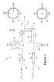
- Figure 3 illustrates one embodiment of the wideband balun structure according to the present invention.
- Figure 4 show the physical layout of one embodiment of the wideband balun structure according to the present invention.
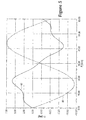
- Figure 5 shows the relative phases of a typical balun and the wideband balun according to the present invention.
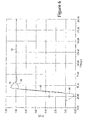
- Figure 6 shows the transient response curves for a typical balun and the wideband balun according to the present invention.
- Figure 7 shows the transient responses of a signal cable, the balun according to the present invention and a system having a combination of the wideband balun and the signal cable.
- Figure 8 shows the frequency responses of a signal cable the balun according to the present invention and a system having a combination of the wideband balun and the signal cable.
- the wideband balun of the present invention uses phase shifters, phase shapers and a 90° hybrid to phase shift the negative going signal of a differential signal 180° at a nominal frequency at the output of the 90° degree hybrid.
- a 90° hybrid to couple a differential amplifier output through a single-ended cable to a single-ended input or equivalently a single-ended amplifier output through a single-ended cable to a differential input
- the 3 dB power loss at DC may be used to compensate for up to 3 dB of cable loss due to high-frequency attenuation in the cable resulting from skin-effect and/or dielectric adsorption.
- the otherwise-wasted high-frequency power may be used in the otherwise-unused output side, coupled through the hybrid, to make up the cable loss, and thus maintain an overall flat response without the additional noise or dynamic range penalties of active cable compensation circuits.
- phase shift networks consisting of phase shifter and phase shapers may be used in one or both legs to broaden or narrow the 90° hybrid's frequency range.
- the non-linear phase response of the phase shapers is tuned to compensate for the frequency-dependent loss in the cable, so as to flatten the system magnitude-vs-frequency response.
- phase shift networks may be used in the single-ended path or both legs of the differential path to tune system phase-vs-frequency response.
- a circuit can be any electrical device having electrical characteristics, such as magnitude versus frequency and phase versus frequency characteristics.
- the system 10 has an overall system characteristics defined by the input and output circuits 12 and 16 and the balun 14.
- the balun 14 according to the present invention has magnitude and phase characteristics that are user defined to set the overall characteristics of the system 10.
- FIG. 2 is block diagram of a signal acquisition probe system 20 for acquiring a signal from a device under test (DUT) 22 and coupling the test signal to a measurement test instrument, such as an oscilloscope, logic analyzer and the like.
- the probe system 20 has a probing head 24 having probing tips or probing cables extending therefrom for connecting to test points on the DUT 22.
- the differential signal under test is coupled to amplifier circuitry 26 in the probing head 24 that amplifies and conditions the test signal for transfer to the measurement test instrument.
- the output of the amplifier circuitry 26 is coupled to differential inputs of a balun 28.
- the balun 28 converts the differential input signal to a single ended output signal.
- the output signal is coupled to a probe cable 30 which is connected to the measurement test instrument.
- the signal acquisition probe system 20 has an uncorrected frequency response that rolls-off as the signal under test frequency increases. This roll-off is mainly due to the losses due to skin and dielectric effects of the cable.
- a novel wideband balun structure is employed having a phase shift and transient response adjusted to compensate for the cable loss as well as broadening the frequency response of the balun.
- Figures 3 and 4 illustrate one embodiment of a wideband balun structure 40 usable with the signal acquisition probe system 20.
- Figure 3 is a schematic representation of the wideband balun structure 40 and Figure 4 is the physical layout of the wideband balun structure 40 on a dielectric substrate 42.
- the positive going differential signal is represented in Figure 3 as having a 0° phase shift and is input to one of the signal paths 44 of the wideband balun structure 40.
- the negative going differential signal is represented in Figure 3 as having a 180° phase shift and is input to the other signal path 46 of the wideband balun structure 40.
- the positive going differential signal is coupled via a circuit trace 48 having ⁇ /2 or 180° phase shift at a nominal frequency to one end of a first order phase shaper 50 having ⁇ /2 or 180° phase shift at the nominal frequency.
- the other end of the first order phase shaper 50 is coupled to a Port 1 input of a 90° hybrid 52.
- the 90° hybrid 52 couples Port 1 with Port 2 that functions as an output port.
- the positive going differential signal at the Port 1 input to the 90° hybrid 52 has been phase shifted 4 ⁇ /4 or 360° from the input signal path 44 input as represented by the phase circle 54.
- the negative going differential signal is coupled, via circuit trace 56 having a ⁇ /4 or 90° phase shift at the nominal frequency, to a second order phase shaper 58 having ⁇ /2 or 180° phase shift at the nominal frequency.
- the other end of the second order phase shaper 58 is coupled to a Port 3 input of the 90° hybrid 52.
- the 90° hybrid 52 couples Port 3 with Port 4.
- Port 4 is coupled to ground via a termination resistor 60.
- the negative going differential signal which is 180° out of phase with the positive going input signal, has been phase shifted 3 ⁇ /4 or 270° at the nominal frequency from the input signal path 46 input.
- the signal at the Port 3 input of the 90° hybrid is phase shifted 450° (180° + 270°) at the nominal frequency relative to the positive going differential signal as represented by the phase circle 62.
- the 90° hybrid 52 has an S-shaped phase response with frequency from its Port 3 input (90° input) to its Port 2 output.
- the phase response of the 90° hybrid 52 from its Port 1 input (0° Input) to its Port 2 output varies linearly with frequency. Accordingly, the phase response at the Port 3 of the 90° hybrid 52 varies with frequency with an associated periodicity.
- the first order phase shaper 50 has a phase response variation with frequency with the same periodicity as the 90° hybrid 52, while the second order phase shaper 58 has a phase response variation with frequency with twice the periodicity of the 90° hybrid 52.
- the combination of the first order phase shifter 50 and the second order phase shaper 58 tunes the output amplitude response of the wideband balun structure 40 with frequency to compensate for the roll-off in the frequency response of the cable 30 with increasing frequency, and.extends the bandwidth of the wideband balun structure 40. This is achieved by reducing the out of phase difference between the positive going differential signal and the inverted negative going input signal through the 90° hybrid so as to increase the signal coupling between the positive going and negative going differential signals outside the normal bandwidth of the 90° hybrid. Further, the phase shapers 50 and 58 correct the phase shift to improve the transient response of the wideband balun 40.
- the wideband balun structure 40 of Figure 4 is implemented using a stripline structure.
- a microstrip structure may also be used in implementing the wideband balun structure 40.
- the wideband balun structure 40 is disposed between two parallel ground planes with the wideband balun structure 40 separated from the parallel ground planes by dielectric layers 42 of which one is shown.
- the dielectric layers 42 are preferably formed of Arlon 350 dielectric material with the stripline structure formed in copper.
- the parallel ground planes are electrically coupled together by vias 72 formed in the dielectric layers.
- the stripline wideband balun structure 40 is deposited on a surface of one of the dielectric layers 42.
- Input pads 74 are formed on the dielectric layer 42 for coupling the signal under test to the signal paths 44 and 46.
- the signal path 44 carrying the positive going differential signal has a somewhat U-shaped circuit trace 48 having a phase shift of 180°.
- the circuit trace 48 is coupled to one end of the 180° first order phase shaper 50.
- the other end of the 180° first order phase shaper is coupled to Port 1 of the 90° hybrid 52.
- the signal path 46 carrying the negative going differential signal has a straight circuit trace 56 having a phase shift of 90°.
- the circuit trace 56 is coupled to one end of a second order phase shaper 58.
- the other end of the second order phase shaper 58 is coupled to Port 3 of the 90° hybrid.
- Port 3 of the 90° hybrid is coupled to Port 4 of the 90° hybrid which in turn is coupled to ground by the termination resistor 60.
- Port 1 of the 90° hybrid is coupled to Port 2 of the 90° hybrid and function as the output port for the wideband balun 40.
- the wideband balun structure 40 has been described as receiving a differential signal and outputting a single end output signal.
- the signal flow of the wideband balun structure may equally be employed for receiving a single ended input signal and outputting a differential output signal.
- a dashed line 80 representing the relative phase of a balun having a 90° hybrid with a 90° phase shift line and a solid line 82 representing the relative phase of the corrected wideband balun structure 40.
- the dashed line 80 shows the relative phase of the differential signal pair going negative with an increase in frequency. This results in the transient response of the 90° hybrid with a 90° phase shift line having pre-shoot 84 prior to the rising edge 86 in the transient response curve as represented by the dashed line 88 in Figure 6 .
- the pre-shoot 84 is caused by the negative going differential signal leading the positive going differential signal in the 90° degree hybrid which causes the 90° hybrid to generate an initial negative output at its port 2 output.
- the solid line 82 shows the relative phase of the differential signal pair going positive with the shape of the positive going relative phase being modified by the first and second order phase shapers 50 and 58 to substantially reduce the pre-shoot prior to the rising edge 90 in the transient response curve of the corrected wideband balun 40 as represented by the solid line 92 in Figure 6 .
- the result of the relative phase of the differential pair going positive substantially reduces the pre-shoot in the transient response curve and causes overshoot 94 in the transient response curve of the corrected wideband balun 40.
- the overshoot 94 is caused by the positive going differential signal leading the negative going differential signal in the 90° degree hybrid which causes the 90° hybrid to generate an initial positive output at its Port 2 output.
- Figure 7 shows the transient responses of a representative cable, such as cable 30 in the signal acquisition probe system 20, the wideband balun 40 of the present invention, and a system having a combination of the wideband balun 40 and the cable 30.
- the dashed line 96 represents the transient response of the wideband balun 40 showing a small aberration 98 at the bottom of the rising edge 100 and overshoot 102 at the top of the rising edge 100.
- the transient response of the wideband balun 40 has a specification allowing for ten percent pre-shoot. This is the result of variations in the manufacturing processes for the wideband balun 40.
- the dotted line 104 represents the transient response of the cable showing a rounded corner 106 at the top of the rising edge 108.
- the solid line 110 represents the combination of the wideband balun 40 and the cable 30. There is no pre-shoot prior to the rising edge 112. The transient response at the top of the rising edge 112 has initial overshoot 114 and then decreases to follow the transient response of the cable 30.
- the frequency response of the cable 30, the wideband balun 40 and a system consisting of the wideband balun 40 and the cable 30 The dashed line 116 represents the frequency response of the wideband balun 40.
- the dotted line 118 represents the frequency response of the cable 30.
- the solid line 120 represents the frequency response of the wideband balun 40 and the cable 30 system.
- the wideband balun 40 frequency response 116 decreases slightly from DC to approximately 8 GHz and then increases approximately 1.6 dBV to 30 GHz.
- the frequency response decreases approximately 0.2 dBV from 30 GHz to 40 GHz and then decreases approximately 1.8 dBV from 40 GHz to 50 GHz.
- the frequency response 118 of the cable 30 decreases approximately 2.7 dBV from DC to 30 GHz and then decreases a further 1.6 dBV from 30 GHz to 39 GHz, whereupon it increases approximately 0.6 dBv to 45 GHz.
- the increasing frequency response 116 of the wideband balun 40 compensates the decreasing frequency response 118 of the cable 30 to produce a balun and cable system response 120 having approximately 1.2 dBV loss from DC to 30 GHz and approximately 1.8 dBv of additional loss from 30 GHz to 44.5 GHz.
Landscapes
- Measuring Leads Or Probes (AREA)
- Dc Digital Transmission (AREA)
- Measurement Of Resistance Or Impedance (AREA)
- Variable-Direction Aerials And Aerial Arrays (AREA)
Abstract
Description
- This application claims the benefit of priority of
US Provisional Application No. 61/509,365, filed 07/19/2011 US Patent Application No. 13/241,916, filed 31/12/2011 US Provisional Application No. 61/509,365 US Patent Application No. 13/241,916 - Broadband DC-coupled amplifiers are generally designed with differential inputs and outputs for reasons such as power supply (and other common-mode) noise immunity, cancelation of even-order harmonic distortion, cancelation of DC offset terms, increased dynamic range due to swing on both outputs, etc. For interconnect between amplifiers on one die, one package, or even on one circuit board, the expense of the differential interconnect is small compared to the advantages of differential design. However, for interconnect between modules, such as between an active probe and an oscilloscope, the cost of differential interconnects is often prohibitive. Not only would two coaxial cables be required rather than one (adding cost and bulk, and reducing flexibility), but the two would also need to be tightly matched to prevent mode conversion from differential to common-mode and vice versa.
- Various passive interconnect structures are known that convert between single-ended and differential signals, often called "baluns" in time-domain applications and/or "180° hybrids" in frequency-domain applications. Broadband, DC-coupled passive baluns are limited to a loss of at least 3 dB, as at DC no energy can be coupled with capacitive or inductive coupling to the "inverted" output, and hence half of the single-ended input power appears as "wasted" common-mode energy at the differential output. Equivalently, for a balun converting a differential input to a single-ended output, half the differential power in the "inverted" input cannot be coupled to the output, and thus is lost. This symmetry can also be inferred from reciprocity of passive elements, with the power loss of a passive balun structure being independent of whether it is used to convert balanced to unbalanced or vice versa.
- Generally, baluns are designed for RF applications and little or no consideration is given to the transient response of the balun. The transient response in such a device may have substantial pre-shoot or pre-shoot and over shoot. However, in certain applications, such as a signal acquisition system having a differential signal acquisition probe coupled to an oscilloscope, the transient response of the balun should have little or no pre-shoot. Further, the balun needs to have a wide bandwidth extending down to DC for coupling a wide range of differential signal to the oscilloscope. In addition, the balun should provide compensation for signal losses in the signal cable of the signal acquisition probe system.
- The wideband balun of the present invention compensates for signal loss caused by a signal cable in a signal acquisition probe system, extends the bandwidth of the wideband balun from DC to system response of at least 15 GHz. In an embodiment, the wideband balun of the present invention provides a transient response having a pre-shoot of no more than ten percent. The wideband balun has a first signal path for a positive going differential signal and a second signal path for a negative going differential signal. A ninety-degree hybrid is coupled to the first signal path for receiving the positive going differential signal at a first port and coupled to the second signal path for receiving the negative going differential signal at a third port. The first port is coupled to a second port of the ninety-degree hybrid coupled and functions as an output port and a fourth port of the ninety-degree hybrid is coupled to the third port and coupled to signal ground via a termination resistor. A phase shaper having a non-linear phase response (i.e. a non-linear variation with frequency of the phase shift between the input signal and the output signal) is inserted into one or both of the first and second signal paths such that the phase differences between the positive going differential signal at the first port and the negative going differential signal at the third port at frequencies from DC to at least 15 GHz compensate for the signal loss caused by the signal cable in a frequency band from DC to at least 15 GHz. In an embodiment, the non-linear phase response of the phase shaper or phase shapers provides for a transient response with less than ten percent pre-shoot.
- In an embodiment, the first signal path of the wideband balun has a circuit trace providing a lambda-over-two phase shift at a nominal frequency in a frequency band from DC to at least 15GHz and a first order phase shaper providing a lambda-over-two phase shift at the nominal frequency resulting in a three hundred and sixty degree phase shift at the nominal frequency at the first port of the ninety degree hybrid. The second signal path has a circuit trace providing a lambda-over-four phase shift at the nominal frequncy and a second order phase shaper providing a lambda-over-two phase shift at the nominal frequency resulting in a two hundred and seventy degree phase shift at the nominal frequency at the output of the second order phase shifter which, when added to the one hundred and eighty degree phase shift of the negative going differential signal, results in a four hundred and fifty degree phase shift at the nominal frequency at the third port of the ninety degree hybrid. The wideband balun is preferably formed as a stripline structure.
- The objects, advantages and novel features of the present invention are apparent from the following detailed description when read in conjunction with appended claims and attached drawings.
-
Figure 1 is a block diagram of an electrical system suitable for use with the wideband balun structure according to the present invention. -
Figure 2 is a block diagram of a signal acquisition probe system using the wideband balun structure according to the present invention. -
Figure 3 illustrates one embodiment of the wideband balun structure according to the present invention. -
Figure 4 show the physical layout of one embodiment of the wideband balun structure according to the present invention. -
Figure 5 shows the relative phases of a typical balun and the wideband balun according to the present invention. -
Figure 6 shows the transient response curves for a typical balun and the wideband balun according to the present invention. -
Figure 7 shows the transient responses of a signal cable, the balun according to the present invention and a system having a combination of the wideband balun and the signal cable. -
Figure 8 shows the frequency responses of a signal cable the balun according to the present invention and a system having a combination of the wideband balun and the signal cable. - The wideband balun of the present invention uses phase shifters, phase shapers and a 90° hybrid to phase shift the negative going signal of a differential signal 180° at a nominal frequency at the output of the 90° degree hybrid. When using a 90° hybrid to couple a differential amplifier output through a single-ended cable to a single-ended input or equivalently a single-ended amplifier output through a single-ended cable to a differential input, the 3 dB power loss at DC may be used to compensate for up to 3 dB of cable loss due to high-frequency attenuation in the cable resulting from skin-effect and/or dielectric adsorption. Put another way, the otherwise-wasted high-frequency power may be used in the otherwise-unused output side, coupled through the hybrid, to make up the cable loss, and thus maintain an overall flat response without the additional noise or dynamic range penalties of active cable compensation circuits.
- The phase shift networks consisting of phase shifter and phase shapers may be used in one or both legs to broaden or narrow the 90° hybrid's frequency range. In this case, the non-linear phase response of the phase shapers is tuned to compensate for the frequency-dependent loss in the cable, so as to flatten the system magnitude-vs-frequency response. Again, phase shift networks may be used in the single-ended path or both legs of the differential path to tune system phase-vs-frequency response.
- Referring to
Figure 1 , there is shown a block diagram of anelectrical system 10 having aninput circuit 12, abalun 14 and anoutput circuit 16. For the purposes of this disclosure, a circuit can be any electrical device having electrical characteristics, such as magnitude versus frequency and phase versus frequency characteristics. Thesystem 10 has an overall system characteristics defined by the input andoutput circuits balun 14. Thebalun 14 according to the present invention has magnitude and phase characteristics that are user defined to set the overall characteristics of thesystem 10. -
Figure 2 is block diagram of a signalacquisition probe system 20 for acquiring a signal from a device under test (DUT) 22 and coupling the test signal to a measurement test instrument, such as an oscilloscope, logic analyzer and the like. Theprobe system 20 has aprobing head 24 having probing tips or probing cables extending therefrom for connecting to test points on theDUT 22. The differential signal under test is coupled toamplifier circuitry 26 in theprobing head 24 that amplifies and conditions the test signal for transfer to the measurement test instrument. The output of theamplifier circuitry 26 is coupled to differential inputs of abalun 28. Thebalun 28 converts the differential input signal to a single ended output signal. The output signal is coupled to aprobe cable 30 which is connected to the measurement test instrument. The signalacquisition probe system 20 has an uncorrected frequency response that rolls-off as the signal under test frequency increases. This roll-off is mainly due to the losses due to skin and dielectric effects of the cable. According to the present invention, a novel wideband balun structure is employed having a phase shift and transient response adjusted to compensate for the cable loss as well as broadening the frequency response of the balun. -
Figures 3 and4 illustrate one embodiment of awideband balun structure 40 usable with the signalacquisition probe system 20.Figure 3 is a schematic representation of thewideband balun structure 40 andFigure 4 is the physical layout of thewideband balun structure 40 on adielectric substrate 42. The positive going differential signal is represented inFigure 3 as having a 0° phase shift and is input to one of thesignal paths 44 of thewideband balun structure 40. The negative going differential signal is represented inFigure 3 as having a 180° phase shift and is input to theother signal path 46 of thewideband balun structure 40. The positive going differential signal is coupled via acircuit trace 48 having λ/2 or 180° phase shift at a nominal frequency to one end of a firstorder phase shaper 50 having λ/2 or 180° phase shift at the nominal frequency. The other end of the firstorder phase shaper 50 is coupled to a Port 1 input of a 90°hybrid 52. Internally, the 90°hybrid 52 couples Port 1 withPort 2 that functions as an output port. At the nominal frequency, the positive going differential signal at the Port 1 input to the 90°hybrid 52 has been phase shifted 4λ/4 or 360° from theinput signal path 44 input as represented by thephase circle 54. - The negative going differential signal is coupled, via
circuit trace 56 having a λ/4 or 90° phase shift at the nominal frequency, to a secondorder phase shaper 58 having λ/2 or 180° phase shift at the nominal frequency. The other end of the secondorder phase shaper 58 is coupled to a Port 3 input of the 90°hybrid 52. Internally, the 90° hybrid 52 couples Port 3 withPort 4.Port 4 is coupled to ground via atermination resistor 60. The negative going differential signal, which is 180° out of phase with the positive going input signal, has been phase shifted 3λ/4 or 270° at the nominal frequency from theinput signal path 46 input. As a result, the signal at the Port 3 input of the 90° hybrid is phase shifted 450° (180° + 270°) at the nominal frequency relative to the positive going differential signal as represented by thephase circle 62. - The 90°
hybrid 52 has an S-shaped phase response with frequency from its Port 3 input (90° input) to itsPort 2 output. The phase response of the 90° hybrid 52 from its Port 1 input (0° Input) to itsPort 2 output varies linearly with frequency. Accordingly, the phase response at the Port 3 of the 90°hybrid 52 varies with frequency with an associated periodicity. The firstorder phase shaper 50 has a phase response variation with frequency with the same periodicity as the 90°hybrid 52, while the secondorder phase shaper 58 has a phase response variation with frequency with twice the periodicity of the 90°hybrid 52. The combination of the firstorder phase shifter 50 and the second order phase shaper 58 tunes the output amplitude response of thewideband balun structure 40 with frequency to compensate for the roll-off in the frequency response of thecable 30 with increasing frequency, and.extends the bandwidth of thewideband balun structure 40. This is achieved by reducing the out of phase difference between the positive going differential signal and the inverted negative going input signal through the 90° hybrid so as to increase the signal coupling between the positive going and negative going differential signals outside the normal bandwidth of the 90° hybrid. Further, thephase shapers wideband balun 40. - The
wideband balun structure 40 ofFigure 4 is implemented using a stripline structure. A microstrip structure may also be used in implementing thewideband balun structure 40. Thewideband balun structure 40 is disposed between two parallel ground planes with thewideband balun structure 40 separated from the parallel ground planes bydielectric layers 42 of which one is shown. The dielectric layers 42 are preferably formed of Arlon 350 dielectric material with the stripline structure formed in copper. The parallel ground planes are electrically coupled together by vias 72 formed in the dielectric layers. The striplinewideband balun structure 40 is deposited on a surface of one of the dielectric layers 42.Input pads 74 are formed on thedielectric layer 42 for coupling the signal under test to thesignal paths signal path 44 carrying the positive going differential signal has a somewhatU-shaped circuit trace 48 having a phase shift of 180°. Thecircuit trace 48 is coupled to one end of the 180° firstorder phase shaper 50. The other end of the 180° first order phase shaper is coupled to Port 1 of the 90°hybrid 52. Thesignal path 46 carrying the negative going differential signal has astraight circuit trace 56 having a phase shift of 90°. Thecircuit trace 56 is coupled to one end of a secondorder phase shaper 58. The other end of the secondorder phase shaper 58 is coupled to Port 3 of the 90° hybrid. Port 3 of the 90° hybrid is coupled toPort 4 of the 90° hybrid which in turn is coupled to ground by thetermination resistor 60. Port 1 of the 90° hybrid is coupled toPort 2 of the 90° hybrid and function as the output port for thewideband balun 40. Thewideband balun structure 40 has been described as receiving a differential signal and outputting a single end output signal. The signal flow of the wideband balun structure may equally be employed for receiving a single ended input signal and outputting a differential output signal. - Referring to
Figure 5 , there is shown a dashedline 80 representing the relative phase of a balun having a 90° hybrid with a 90° phase shift line and asolid line 82 representing the relative phase of the correctedwideband balun structure 40. The dashedline 80 shows the relative phase of the differential signal pair going negative with an increase in frequency. This results in the transient response of the 90° hybrid with a 90° phase shiftline having pre-shoot 84 prior to the risingedge 86 in the transient response curve as represented by the dashedline 88 inFigure 6 . The pre-shoot 84 is caused by the negative going differential signal leading the positive going differential signal in the 90° degree hybrid which causes the 90° hybrid to generate an initial negative output at itsport 2 output. - The
solid line 82 shows the relative phase of the differential signal pair going positive with the shape of the positive going relative phase being modified by the first and secondorder phase shapers edge 90 in the transient response curve of the correctedwideband balun 40 as represented by thesolid line 92 inFigure 6 . The result of the relative phase of the differential pair going positive substantially reduces the pre-shoot in the transient response curve and causesovershoot 94 in the transient response curve of the correctedwideband balun 40. Theovershoot 94 is caused by the positive going differential signal leading the negative going differential signal in the 90° degree hybrid which causes the 90° hybrid to generate an initial positive output at itsPort 2 output. -
Figure 7 shows the transient responses of a representative cable, such ascable 30 in the signalacquisition probe system 20, thewideband balun 40 of the present invention, and a system having a combination of thewideband balun 40 and thecable 30. The dashedline 96 represents the transient response of thewideband balun 40 showing asmall aberration 98 at the bottom of the risingedge 100 and overshoot 102 at the top of the risingedge 100. As can be seen by the dashed line, there is substantially no pre-shoot in the transient response of thewideband balun 40. In actual implementation, the transient response of thewideband balun 40 has a specification allowing for ten percent pre-shoot. This is the result of variations in the manufacturing processes for thewideband balun 40. The dottedline 104 represents the transient response of the cable showing arounded corner 106 at the top of the risingedge 108. Thesolid line 110 represents the combination of thewideband balun 40 and thecable 30. There is no pre-shoot prior to the risingedge 112. The transient response at the top of the risingedge 112 hasinitial overshoot 114 and then decreases to follow the transient response of thecable 30. - Referring to
Figure 8 , there is shown the frequency response of thecable 30, thewideband balun 40 and a system consisting of thewideband balun 40 and thecable 30. The dashedline 116 represents the frequency response of thewideband balun 40. The dottedline 118 represents the frequency response of thecable 30. Thesolid line 120 represents the frequency response of thewideband balun 40 and thecable 30 system. Thewideband balun 40frequency response 116 decreases slightly from DC to approximately 8 GHz and then increases approximately 1.6 dBV to 30 GHz. The frequency response decreases approximately 0.2 dBV from 30 GHz to 40 GHz and then decreases approximately 1.8 dBV from 40 GHz to 50 GHz. Thefrequency response 118 of thecable 30 decreases approximately 2.7 dBV from DC to 30 GHz and then decreases a further 1.6 dBV from 30 GHz to 39 GHz, whereupon it increases approximately 0.6 dBv to 45 GHz. The increasingfrequency response 116 of thewideband balun 40 compensates the decreasingfrequency response 118 of thecable 30 to produce a balun andcable system response 120 having approximately 1.2 dBV loss from DC to 30 GHz and approximately 1.8 dBv of additional loss from 30 GHz to 44.5 GHz. - It will be obvious to those having skill in the art that many changes may be made to the details of the above-described embodiments of this invention without departing from the underlying principles thereof. The scope of the present invention should, therefore, be determined only by the following claims
Claims (6)
- A wideband balun structure comprising:a first signal path for a positive going differential signal and a second signal path for a negative going differential signal; anda ninety-degree hybrid coupled to the first signal path for receiving the positive going differential signal at a first port and coupled to the second signal path for receiving the negative going differential signal at a second port with a third port of the ninety-degree hybrid coupled to the first port and functioning as an output port and a fourth port of the ninety-degree hybrid coupled to the second port and coupled to signal ground via a termination resistor; anda signal cable coupled to the output port;wherein at least one of the first signal path and the second signal path comprises a phase shifter having a non-linear phase response tuned to compensate for the signal loss caused by the signal cable and providing a frequency band from DC to at least 15 GHz.
- A wideband balun structure according to claim 1, wherein at least one of the first signal path and the second signal path has a non-linear phase response tuned to provide a transient response in the frequency band from DC to at least 15GHz having less than ten percent pre-shoot.
- A wideband balun structure according to claim 1 or 2, wherein the first signal path comprises a phase shifter having a non-linear phase response having the same periodicity as the ninety-degree hybrid and the second signal path comprises a phase shifter having a non-linear phase response having a periodicity twice that of the ninety-degree phase shifter.
- The wide bandwidth balun structure as recited in any preceding claim wherein the first signal path has a circuit trace providing a lambda-over-two phase shift at a nominal frequency and a phase shifter having a non-linear phase response providing a lambda-over-two phase shift at the nominal frequency resulting in a three hundred and sixty degree phase shift at the nominal frequency at Port 1 of the ninety degree hybrid.
- The wide bandwidth balun structure as recited in any preceding claim wherein the second signal path has a circuit trace providing a lambda-over-four phase shift at a nominal frequency and a phase shifter having a non-linear phase response providing a lambda-over-two phase shift at the nominal frequency resulting in a two hundred and seventy degree phase shift at the nominal frequency at the output of the phase shifter in the second signal path, which when added to the one hundred and eighty degree phase shift of the negative going differential signal results in a four hundred and fifty degree phase shift at the nominal frequency at Port 2 of the ninety degree hybrid.
- The wide bandwidth balun structure as recited in any preceding claim wherein the balun structure is formed as a stripline structure.
Applications Claiming Priority (2)
| Application Number | Priority Date | Filing Date | Title |
|---|---|---|---|
| US201161509365P | 2011-07-19 | 2011-07-19 | |
| US13/341,916 US8611436B2 (en) | 2011-07-19 | 2011-12-31 | Wideband balun structure |
Publications (3)
| Publication Number | Publication Date |
|---|---|
| EP2549584A2 true EP2549584A2 (en) | 2013-01-23 |
| EP2549584A3 EP2549584A3 (en) | 2013-04-17 |
| EP2549584B1 EP2549584B1 (en) | 2016-10-26 |
Family
ID=47074571
Family Applications (1)
| Application Number | Title | Priority Date | Filing Date |
|---|---|---|---|
| EP12176962.4A Active EP2549584B1 (en) | 2011-07-19 | 2012-07-18 | Wideband balun structure |
Country Status (6)
| Country | Link |
|---|---|
| US (1) | US8611436B2 (en) |
| EP (1) | EP2549584B1 (en) |
| JP (1) | JP6200635B2 (en) |
| KR (1) | KR101911019B1 (en) |
| CN (1) | CN102891676B (en) |
| TW (1) | TWI552523B (en) |
Cited By (1)
| Publication number | Priority date | Publication date | Assignee | Title |
|---|---|---|---|---|
| CN109546987A (en) * | 2018-11-16 | 2019-03-29 | 西安电子科技大学 | Broadband active phase shifter |
Families Citing this family (7)
| Publication number | Priority date | Publication date | Assignee | Title |
|---|---|---|---|---|
| US9634639B2 (en) * | 2015-09-10 | 2017-04-25 | Harris Corporation | Tunable electronic circuit which converts balanced signals to unbalanced signals |
| CN108900172B (en) * | 2018-06-05 | 2021-09-28 | 东南大学 | Broadband single-ended input high-precision quadrature differential output signal generation circuit |
| US10886588B2 (en) | 2018-09-26 | 2021-01-05 | Keysight Technologies, Inc. | High dynamic range probe using pole-zero cancellation |
| KR102837328B1 (en) | 2020-07-29 | 2025-07-23 | 삼성전자주식회사 | Antenna module possible to support wideband and base station including the antenna module |
| WO2024051947A1 (en) * | 2022-09-08 | 2024-03-14 | Alcan Systems Gmbh | Radio frequency device |
| US20240339742A1 (en) * | 2023-04-07 | 2024-10-10 | Tektronix, Inc. | Compact balun structure for broadband time-domain applications |
| CN116799463A (en) | 2023-08-02 | 2023-09-22 | 南开大学 | New broadband balun structure and its application |
Family Cites Families (21)
| Publication number | Priority date | Publication date | Assignee | Title |
|---|---|---|---|---|
| JPS61205002A (en) * | 1985-03-08 | 1986-09-11 | Nec Corp | Electric power distributor |
| US5148130A (en) * | 1990-06-07 | 1992-09-15 | Dietrich James L | Wideband microstrip UHF balun |
| US5345471A (en) * | 1993-04-12 | 1994-09-06 | The Regents Of The University Of California | Ultra-wideband receiver |
| US5764195A (en) * | 1996-07-24 | 1998-06-09 | Hazeltine Corporation | UHF/VHF multifunction ocean antenna system |
| US5945890A (en) * | 1997-06-16 | 1999-08-31 | The United States Of America As Represented By The Secretary Of The Army | Ultra-wide bandwidth field stacking balun |
| US6140886A (en) * | 1999-02-25 | 2000-10-31 | Lucent Technologies, Inc. | Wideband balun for wireless and RF application |
| US6292070B1 (en) * | 1999-03-11 | 2001-09-18 | Anaren Microwave, Inc. | Balun formed from symmetrical couplers and method for making same |
| US7356077B2 (en) * | 2001-09-07 | 2008-04-08 | Spirent Communications Inc. | Method and apparatus for testing network integrity |
| US6982609B1 (en) * | 2002-05-15 | 2006-01-03 | Zeevo | System method and apparatus for a three-line balun with power amplifier bias |
| US6844792B1 (en) * | 2002-05-15 | 2005-01-18 | Zeevo | Single ended tuning of a differential power amplifier output |
| US6946880B2 (en) * | 2003-03-27 | 2005-09-20 | Raytheon Company | Compact balun for rejecting common mode electromagnetic fields |
| US20050084033A1 (en) * | 2003-08-04 | 2005-04-21 | Lowell Rosen | Scalable transform wideband holographic communications apparatus and methods |
| JP2005176334A (en) * | 2003-11-17 | 2005-06-30 | Mitsubishi Electric Corp | Balun circuit |
| US7068122B2 (en) * | 2004-09-28 | 2006-06-27 | Industrial Technology Research Institute | Miniaturized multi-layer balun |
| US7567142B2 (en) * | 2005-06-24 | 2009-07-28 | Atheros Communications, Inc. | Quasi-balun |
| US7969372B2 (en) * | 2006-08-03 | 2011-06-28 | Panasonic Corporation | Antenna apparatus utilizing small loop antenna element having minute length and two feeding points |
| US7795889B2 (en) * | 2008-01-25 | 2010-09-14 | Infineon Technologies Ag | Probe device |
| JP2009260444A (en) * | 2008-04-11 | 2009-11-05 | Toshiba Corp | Power combiner, amplifier, and transmitter |
| US7961048B2 (en) * | 2008-12-12 | 2011-06-14 | Samsung Electro-Mechanics Company | Integrated power amplifiers for use in wireless communication devices |
| US8125270B2 (en) * | 2009-05-11 | 2012-02-28 | The Board Of Trustees Of The Leland Stanford Junior University | Frequency offset Cartesian feedback system |
| CN102710219B (en) * | 2012-05-25 | 2014-11-26 | 姜鑫 | Passive three-balanced frequency converter |
-
2011
- 2011-12-31 US US13/341,916 patent/US8611436B2/en active Active
-
2012
- 2012-07-12 TW TW101125097A patent/TWI552523B/en active
- 2012-07-17 CN CN201210246902.4A patent/CN102891676B/en active Active
- 2012-07-18 EP EP12176962.4A patent/EP2549584B1/en active Active
- 2012-07-18 KR KR1020120078212A patent/KR101911019B1/en active Active
- 2012-07-19 JP JP2012160552A patent/JP6200635B2/en active Active
Non-Patent Citations (1)
| Title |
|---|
| None |
Cited By (1)
| Publication number | Priority date | Publication date | Assignee | Title |
|---|---|---|---|---|
| CN109546987A (en) * | 2018-11-16 | 2019-03-29 | 西安电子科技大学 | Broadband active phase shifter |
Also Published As
| Publication number | Publication date |
|---|---|
| KR20130010863A (en) | 2013-01-29 |
| US20130022133A1 (en) | 2013-01-24 |
| JP2013027048A (en) | 2013-02-04 |
| US8611436B2 (en) | 2013-12-17 |
| EP2549584B1 (en) | 2016-10-26 |
| KR101911019B1 (en) | 2018-12-19 |
| EP2549584A3 (en) | 2013-04-17 |
| TW201325080A (en) | 2013-06-16 |
| TWI552523B (en) | 2016-10-01 |
| CN102891676A (en) | 2013-01-23 |
| JP6200635B2 (en) | 2017-09-20 |
| CN102891676B (en) | 2017-04-12 |
Similar Documents
| Publication | Publication Date | Title |
|---|---|---|
| EP2549584B1 (en) | Wideband balun structure | |
| US10003318B2 (en) | Circuit | |
| US9300022B2 (en) | Vaisman baluns and microwave devices employing the same | |
| US20100182096A1 (en) | Ultra-Wideband Balun and Application Module Thereof | |
| US20130033336A1 (en) | Unbalanced-balanced conversion circuit element | |
| Hossain et al. | A compact broadband Marchand balun for millimeter-wave and sub-THz applications | |
| CN104319450A (en) | Ultra wide band bridge based on thick film manufacturing technology | |
| US8362849B2 (en) | Broadband balun | |
| US9148113B2 (en) | Balanced-to-unbalanced converter | |
| Sakai et al. | A 220–330 GHz wideband, low-loss and small Marchand balun with ground shields in SiGe BiCMOS technology | |
| CN107039729A (en) | Metal ground structure in wideband balun | |
| KR101559721B1 (en) | Wideband microwave balun with high isolation properties | |
| Sakai et al. | A 135 GHz CMOS Marchand balun with ground sheilds | |
| US20180090806A1 (en) | Bandwidth increase method for differential passive elements | |
| Triantafyllos et al. | A 220–340 GHz Modified Marchand Balun With Asymmetric Ground Shield in 90-nm SiGe-BiCMOS | |
| CN118944685B (en) | A SiP chip for radio frequency and digital-analog hybrid circuits | |
| Wu et al. | A 71–76 GHz Four-Element Phased-Array Receiver with Compact Footprint in 65-nm CMOS | |
| Liu et al. | A Ku-band 65nm CMOS VSWR Alarm Circuit Based on Power Detection | |
| JP5047027B2 (en) | Image enhanced mixer circuit | |
| Lin et al. | Metamaterial-based Wilkinson balun using asymmetrical T-structure power divider for improving phase response flatness | |
| JP2017220635A (en) | Printed circuit board | |
| CN104360125B (en) | A kind of orientation electric bridge based on coupled capacitor | |
| TW201404034A (en) | Power amplification device and coupler | |
| CN103000337A (en) | Balun transformer |
Legal Events
| Date | Code | Title | Description |
|---|---|---|---|
| PUAI | Public reference made under article 153(3) epc to a published international application that has entered the european phase |
Free format text: ORIGINAL CODE: 0009012 |
|
| AK | Designated contracting states |
Kind code of ref document: A2 Designated state(s): AL AT BE BG CH CY CZ DE DK EE ES FI FR GB GR HR HU IE IS IT LI LT LU LV MC MK MT NL NO PL PT RO RS SE SI SK SM TR |
|
| AX | Request for extension of the european patent |
Extension state: BA ME |
|
| PUAL | Search report despatched |
Free format text: ORIGINAL CODE: 0009013 |
|
| AK | Designated contracting states |
Kind code of ref document: A3 Designated state(s): AL AT BE BG CH CY CZ DE DK EE ES FI FR GB GR HR HU IE IS IT LI LT LU LV MC MK MT NL NO PL PT RO RS SE SI SK SM TR |
|
| AX | Request for extension of the european patent |
Extension state: BA ME |
|
| RIC1 | Information provided on ipc code assigned before grant |
Ipc: H01P 5/18 20060101ALI20130312BHEP Ipc: H01P 1/18 20060101AFI20130312BHEP Ipc: H01P 5/10 20060101ALI20130312BHEP |
|
| 17P | Request for examination filed |
Effective date: 20131017 |
|
| RBV | Designated contracting states (corrected) |
Designated state(s): AL AT BE BG CH CY CZ DE DK EE ES FI FR GB GR HR HU IE IS IT LI LT LU LV MC MK MT NL NO PL PT RO RS SE SI SK SM TR |
|
| RAP1 | Party data changed (applicant data changed or rights of an application transferred) |
Owner name: TEKTRONIX, INC. |
|
| GRAP | Despatch of communication of intention to grant a patent |
Free format text: ORIGINAL CODE: EPIDOSNIGR1 |
|
| INTG | Intention to grant announced |
Effective date: 20160728 |
|
| GRAS | Grant fee paid |
Free format text: ORIGINAL CODE: EPIDOSNIGR3 |
|
| GRAA | (expected) grant |
Free format text: ORIGINAL CODE: 0009210 |
|
| AK | Designated contracting states |
Kind code of ref document: B1 Designated state(s): AL AT BE BG CH CY CZ DE DK EE ES FI FR GB GR HR HU IE IS IT LI LT LU LV MC MK MT NL NO PL PT RO RS SE SI SK SM TR |
|
| REG | Reference to a national code |
Ref country code: GB Ref legal event code: FG4D |
|
| REG | Reference to a national code |
Ref country code: CH Ref legal event code: EP |
|
| REG | Reference to a national code |
Ref country code: AT Ref legal event code: REF Ref document number: 840604 Country of ref document: AT Kind code of ref document: T Effective date: 20161115 |
|
| REG | Reference to a national code |
Ref country code: IE Ref legal event code: FG4D |
|
| REG | Reference to a national code |
Ref country code: DE Ref legal event code: R096 Ref document number: 602012024523 Country of ref document: DE |
|
| REG | Reference to a national code |
Ref country code: LT Ref legal event code: MG4D |
|
| PG25 | Lapsed in a contracting state [announced via postgrant information from national office to epo] |
Ref country code: LV Free format text: LAPSE BECAUSE OF FAILURE TO SUBMIT A TRANSLATION OF THE DESCRIPTION OR TO PAY THE FEE WITHIN THE PRESCRIBED TIME-LIMIT Effective date: 20161026 |
|
| REG | Reference to a national code |
Ref country code: NL Ref legal event code: MP Effective date: 20161026 |
|
| REG | Reference to a national code |
Ref country code: AT Ref legal event code: MK05 Ref document number: 840604 Country of ref document: AT Kind code of ref document: T Effective date: 20161026 |
|
| PG25 | Lapsed in a contracting state [announced via postgrant information from national office to epo] |
Ref country code: GR Free format text: LAPSE BECAUSE OF FAILURE TO SUBMIT A TRANSLATION OF THE DESCRIPTION OR TO PAY THE FEE WITHIN THE PRESCRIBED TIME-LIMIT Effective date: 20170127 Ref country code: LT Free format text: LAPSE BECAUSE OF FAILURE TO SUBMIT A TRANSLATION OF THE DESCRIPTION OR TO PAY THE FEE WITHIN THE PRESCRIBED TIME-LIMIT Effective date: 20161026 Ref country code: NO Free format text: LAPSE BECAUSE OF FAILURE TO SUBMIT A TRANSLATION OF THE DESCRIPTION OR TO PAY THE FEE WITHIN THE PRESCRIBED TIME-LIMIT Effective date: 20170126 Ref country code: SE Free format text: LAPSE BECAUSE OF FAILURE TO SUBMIT A TRANSLATION OF THE DESCRIPTION OR TO PAY THE FEE WITHIN THE PRESCRIBED TIME-LIMIT Effective date: 20161026 |
|
| PG25 | Lapsed in a contracting state [announced via postgrant information from national office to epo] |
Ref country code: IS Free format text: LAPSE BECAUSE OF FAILURE TO SUBMIT A TRANSLATION OF THE DESCRIPTION OR TO PAY THE FEE WITHIN THE PRESCRIBED TIME-LIMIT Effective date: 20170226 Ref country code: RS Free format text: LAPSE BECAUSE OF FAILURE TO SUBMIT A TRANSLATION OF THE DESCRIPTION OR TO PAY THE FEE WITHIN THE PRESCRIBED TIME-LIMIT Effective date: 20161026 Ref country code: PL Free format text: LAPSE BECAUSE OF FAILURE TO SUBMIT A TRANSLATION OF THE DESCRIPTION OR TO PAY THE FEE WITHIN THE PRESCRIBED TIME-LIMIT Effective date: 20161026 Ref country code: AT Free format text: LAPSE BECAUSE OF FAILURE TO SUBMIT A TRANSLATION OF THE DESCRIPTION OR TO PAY THE FEE WITHIN THE PRESCRIBED TIME-LIMIT Effective date: 20161026 Ref country code: BE Free format text: LAPSE BECAUSE OF FAILURE TO SUBMIT A TRANSLATION OF THE DESCRIPTION OR TO PAY THE FEE WITHIN THE PRESCRIBED TIME-LIMIT Effective date: 20161026 Ref country code: NL Free format text: LAPSE BECAUSE OF FAILURE TO SUBMIT A TRANSLATION OF THE DESCRIPTION OR TO PAY THE FEE WITHIN THE PRESCRIBED TIME-LIMIT Effective date: 20161026 Ref country code: HR Free format text: LAPSE BECAUSE OF FAILURE TO SUBMIT A TRANSLATION OF THE DESCRIPTION OR TO PAY THE FEE WITHIN THE PRESCRIBED TIME-LIMIT Effective date: 20161026 Ref country code: PT Free format text: LAPSE BECAUSE OF FAILURE TO SUBMIT A TRANSLATION OF THE DESCRIPTION OR TO PAY THE FEE WITHIN THE PRESCRIBED TIME-LIMIT Effective date: 20170227 Ref country code: FI Free format text: LAPSE BECAUSE OF FAILURE TO SUBMIT A TRANSLATION OF THE DESCRIPTION OR TO PAY THE FEE WITHIN THE PRESCRIBED TIME-LIMIT Effective date: 20161026 Ref country code: ES Free format text: LAPSE BECAUSE OF FAILURE TO SUBMIT A TRANSLATION OF THE DESCRIPTION OR TO PAY THE FEE WITHIN THE PRESCRIBED TIME-LIMIT Effective date: 20161026 |
|
| REG | Reference to a national code |
Ref country code: DE Ref legal event code: R097 Ref document number: 602012024523 Country of ref document: DE |
|
| PG25 | Lapsed in a contracting state [announced via postgrant information from national office to epo] |
Ref country code: EE Free format text: LAPSE BECAUSE OF FAILURE TO SUBMIT A TRANSLATION OF THE DESCRIPTION OR TO PAY THE FEE WITHIN THE PRESCRIBED TIME-LIMIT Effective date: 20161026 Ref country code: SK Free format text: LAPSE BECAUSE OF FAILURE TO SUBMIT A TRANSLATION OF THE DESCRIPTION OR TO PAY THE FEE WITHIN THE PRESCRIBED TIME-LIMIT Effective date: 20161026 Ref country code: CZ Free format text: LAPSE BECAUSE OF FAILURE TO SUBMIT A TRANSLATION OF THE DESCRIPTION OR TO PAY THE FEE WITHIN THE PRESCRIBED TIME-LIMIT Effective date: 20161026 Ref country code: RO Free format text: LAPSE BECAUSE OF FAILURE TO SUBMIT A TRANSLATION OF THE DESCRIPTION OR TO PAY THE FEE WITHIN THE PRESCRIBED TIME-LIMIT Effective date: 20161026 Ref country code: DK Free format text: LAPSE BECAUSE OF FAILURE TO SUBMIT A TRANSLATION OF THE DESCRIPTION OR TO PAY THE FEE WITHIN THE PRESCRIBED TIME-LIMIT Effective date: 20161026 |
|
| PG25 | Lapsed in a contracting state [announced via postgrant information from national office to epo] |
Ref country code: IT Free format text: LAPSE BECAUSE OF FAILURE TO SUBMIT A TRANSLATION OF THE DESCRIPTION OR TO PAY THE FEE WITHIN THE PRESCRIBED TIME-LIMIT Effective date: 20161026 Ref country code: BG Free format text: LAPSE BECAUSE OF FAILURE TO SUBMIT A TRANSLATION OF THE DESCRIPTION OR TO PAY THE FEE WITHIN THE PRESCRIBED TIME-LIMIT Effective date: 20170126 Ref country code: SM Free format text: LAPSE BECAUSE OF FAILURE TO SUBMIT A TRANSLATION OF THE DESCRIPTION OR TO PAY THE FEE WITHIN THE PRESCRIBED TIME-LIMIT Effective date: 20161026 |
|
| PLBE | No opposition filed within time limit |
Free format text: ORIGINAL CODE: 0009261 |
|
| STAA | Information on the status of an ep patent application or granted ep patent |
Free format text: STATUS: NO OPPOSITION FILED WITHIN TIME LIMIT |
|
| 26N | No opposition filed |
Effective date: 20170727 |
|
| PG25 | Lapsed in a contracting state [announced via postgrant information from national office to epo] |
Ref country code: SI Free format text: LAPSE BECAUSE OF FAILURE TO SUBMIT A TRANSLATION OF THE DESCRIPTION OR TO PAY THE FEE WITHIN THE PRESCRIBED TIME-LIMIT Effective date: 20161026 |
|
| REG | Reference to a national code |
Ref country code: CH Ref legal event code: PL |
|
| REG | Reference to a national code |
Ref country code: IE Ref legal event code: MM4A |
|
| REG | Reference to a national code |
Ref country code: FR Ref legal event code: ST Effective date: 20180330 |
|
| PG25 | Lapsed in a contracting state [announced via postgrant information from national office to epo] |
Ref country code: IE Free format text: LAPSE BECAUSE OF NON-PAYMENT OF DUE FEES Effective date: 20170718 Ref country code: CH Free format text: LAPSE BECAUSE OF NON-PAYMENT OF DUE FEES Effective date: 20170731 Ref country code: LI Free format text: LAPSE BECAUSE OF NON-PAYMENT OF DUE FEES Effective date: 20170731 |
|
| PG25 | Lapsed in a contracting state [announced via postgrant information from national office to epo] |
Ref country code: FR Free format text: LAPSE BECAUSE OF NON-PAYMENT OF DUE FEES Effective date: 20170731 |
|
| PG25 | Lapsed in a contracting state [announced via postgrant information from national office to epo] |
Ref country code: LU Free format text: LAPSE BECAUSE OF NON-PAYMENT OF DUE FEES Effective date: 20170718 |
|
| PG25 | Lapsed in a contracting state [announced via postgrant information from national office to epo] |
Ref country code: MT Free format text: LAPSE BECAUSE OF NON-PAYMENT OF DUE FEES Effective date: 20170718 |
|
| PGFP | Annual fee paid to national office [announced via postgrant information from national office to epo] |
Ref country code: GB Payment date: 20180727 Year of fee payment: 7 |
|
| PG25 | Lapsed in a contracting state [announced via postgrant information from national office to epo] |
Ref country code: MC Free format text: LAPSE BECAUSE OF FAILURE TO SUBMIT A TRANSLATION OF THE DESCRIPTION OR TO PAY THE FEE WITHIN THE PRESCRIBED TIME-LIMIT Effective date: 20161026 Ref country code: HU Free format text: LAPSE BECAUSE OF FAILURE TO SUBMIT A TRANSLATION OF THE DESCRIPTION OR TO PAY THE FEE WITHIN THE PRESCRIBED TIME-LIMIT; INVALID AB INITIO Effective date: 20120718 |
|
| PG25 | Lapsed in a contracting state [announced via postgrant information from national office to epo] |
Ref country code: CY Free format text: LAPSE BECAUSE OF NON-PAYMENT OF DUE FEES Effective date: 20161026 |
|
| PG25 | Lapsed in a contracting state [announced via postgrant information from national office to epo] |
Ref country code: MK Free format text: LAPSE BECAUSE OF FAILURE TO SUBMIT A TRANSLATION OF THE DESCRIPTION OR TO PAY THE FEE WITHIN THE PRESCRIBED TIME-LIMIT Effective date: 20161026 |
|
| GBPC | Gb: european patent ceased through non-payment of renewal fee |
Effective date: 20190718 |
|
| PG25 | Lapsed in a contracting state [announced via postgrant information from national office to epo] |
Ref country code: TR Free format text: LAPSE BECAUSE OF FAILURE TO SUBMIT A TRANSLATION OF THE DESCRIPTION OR TO PAY THE FEE WITHIN THE PRESCRIBED TIME-LIMIT Effective date: 20161026 |
|
| PG25 | Lapsed in a contracting state [announced via postgrant information from national office to epo] |
Ref country code: GB Free format text: LAPSE BECAUSE OF NON-PAYMENT OF DUE FEES Effective date: 20190718 |
|
| PG25 | Lapsed in a contracting state [announced via postgrant information from national office to epo] |
Ref country code: AL Free format text: LAPSE BECAUSE OF FAILURE TO SUBMIT A TRANSLATION OF THE DESCRIPTION OR TO PAY THE FEE WITHIN THE PRESCRIBED TIME-LIMIT Effective date: 20161026 |
|
| P01 | Opt-out of the competence of the unified patent court (upc) registered |
Effective date: 20230530 |
|
| PGFP | Annual fee paid to national office [announced via postgrant information from national office to epo] |
Ref country code: DE Payment date: 20250729 Year of fee payment: 14 |