EP2546837A1 - Verfahren zum Erkennen von gelöschten Speicherbereichen - Google Patents
Verfahren zum Erkennen von gelöschten Speicherbereichen Download PDFInfo
- Publication number
- EP2546837A1 EP2546837A1 EP12002829A EP12002829A EP2546837A1 EP 2546837 A1 EP2546837 A1 EP 2546837A1 EP 12002829 A EP12002829 A EP 12002829A EP 12002829 A EP12002829 A EP 12002829A EP 2546837 A1 EP2546837 A1 EP 2546837A1
- Authority
- EP
- European Patent Office
- Prior art keywords
- memory
- erased
- memory areas
- areas
- target number
- Prior art date
- Legal status (The legal status is an assumption and is not a legal conclusion. Google has not performed a legal analysis and makes no representation as to the accuracy of the status listed.)
- Granted
Links
Images
Classifications
-
- G—PHYSICS
- G11—INFORMATION STORAGE
- G11C—STATIC STORES
- G11C16/00—Erasable programmable read-only memories
- G11C16/02—Erasable programmable read-only memories electrically programmable
- G11C16/06—Auxiliary circuits, e.g. for writing into memory
- G11C16/10—Programming or data input circuits
- G11C16/14—Circuits for erasing electrically, e.g. erase voltage switching circuits
-
- G—PHYSICS
- G06—COMPUTING OR CALCULATING; COUNTING
- G06F—ELECTRIC DIGITAL DATA PROCESSING
- G06F12/00—Accessing, addressing or allocating within memory systems or architectures
- G06F12/02—Addressing or allocation; Relocation
- G06F12/0223—User address space allocation, e.g. contiguous or non contiguous base addressing
- G06F12/023—Free address space management
- G06F12/0238—Memory management in non-volatile memory, e.g. resistive RAM or ferroelectric memory
- G06F12/0246—Memory management in non-volatile memory, e.g. resistive RAM or ferroelectric memory in block erasable memory, e.g. flash memory
-
- G—PHYSICS
- G06—COMPUTING OR CALCULATING; COUNTING
- G06F—ELECTRIC DIGITAL DATA PROCESSING
- G06F2212/00—Indexing scheme relating to accessing, addressing or allocation within memory systems or architectures
- G06F2212/17—Embedded application
- G06F2212/177—Smart card
Definitions
- the invention relates to a method for error analysis on an electronic memory subdivided into memory areas, in particular for detecting falsely erased memory areas in the memory, e.g. a flash memory divided into pages (pages).
- Flash memories are divided into pages (pages) which currently have a typical size of 256 bytes, i. 256 * 8 individual memory cells, have.
- the chip card has in addition to the flash memory, in particular a processor and a random access memory RAM.
- Each memory cell of the flash memory can accept, write and erase two memory states.
- a byte-by-byte (possibly also bit or wordwise) driving of the flash memory is only possible during writing, i. when programming the memory in the described state, possible.
- a write command which is sent to the memory, for example, by a chip card operating system, is therefore converted into memory in two programming steps, namely an erase operation performed first and a subsequent write operation.
- the deletion process the entire memory page on which the memory cells / bytes to be written are arranged is copied to a buffer memory and then deleted.
- the memory cells specified in the write command are programmed into the described memory state.
- an atomic write which is chosen especially for important memory contents, as a buffer for the memory page to be deleted another memory page is used in the non-volatile but slow flash memory.
- non-atomic write operations are selected in which a memory area in the fast but volatile random access memory RAM is used as a buffer memory for the memory page to be deleted.
- the lack of memory content of the erased and non-rewritten memory page may result in data loss or even compromise memory performance, especially if portions of an operating system stored in flash memory have been erased.
- flash memory is tight, it happens that in the flash memory partly on a single memory page both data that are changed more frequently, as well as parts of the operating system are stored.
- Each change of data by means of a non-atomic write command can therefore endanger the operating system and thus not only the memory itself but also further components of the chip card.
- a direct reading access to the flash memory of a smart card from outside the smart card is no longer possible after issuing the smart card for security reasons.
- the flash memory can not be checked directly for falsely erased memory pages.
- the invention is based on the object of providing a method for error analysis on an electronic memory subdivided into memory areas, in particular for detecting incorrectly erased memory areas in the memory, e.g. a flash memory partitioned into pages (pages).
- a programmer may at least exclude other causes of errors and possibly reconstruct the lost memory contents and thus render the memory or its memory contents functional again.
- the actual number and the target number - and possibly the identification characters, cf. below - provided to a terminal configured to communicate with the memory, for example, a memory in a smart card to a smart card terminal.
- the comparison of the actual number and the target number is performed in the terminal.
- each write command comprises a first erase operation and a subsequent write operation.
- each memory area is divided into memory cells, which in turn are optionally grouped into bytes or words within the memory area.
- only an entire memory area can be deleted during an erase process, but not individual memory cells, bytes or words.
- individual memory cells or bytes or words may be described.
- the memory is a flash memory and the memory areas are memory pages in the flash memory.
- the flash memory has the properties described in the preceding paragraph.
- the step b) determining an actual number of erased memory areas is optionally performed as counting memory areas having a memory content corresponding to a cleared state of the respective memory area.
- a typical erasure process in flash memory takes four milliseconds and thus a relatively long time.
- a typical write in a Flash memory takes about ten microseconds and thus relatively short.
- the memory page in the flash memory is erased, more specifically erroneously erased, and thus has a cleared memory state.
- the likelihood of the voltage drop occurring during the writing process is low because of the short duration of the writing operation. Thus, the probability is low that the memory page is partially described after a power failure.
- the step a) determining a target number of erased memory areas is optionally performed as setting the target number of erased memory areas to zero.
- the above embodiment will be explained with reference to a smart card having a flash memory divided into memory pages.
- the available flash memory is usually tight. Therefore, the Flash memory is usually full and has no empty memory pages when intact.
- the target number of erased memory pages in the flash memory of such a smart card is zero. If the actual number of erased memory pages determined according to step b) is not equal to zero, this means that erroneously erased memory pages exist, ie memory pages that should actually be written. For other memories subdivided into memory areas, what has been said applies analogously.
- the step a) determining a target number of erased memory areas is performed as determining a number of previously executed erase commands (erase commands).
- Deleted memory areas can be generated by a delete command.
- an erase command an erase operation is performed on a memory area without subsequently performing a write operation.
- an empty or erased memory area is generated with each erase command. If there are more erased areas in the memory than erase commands, then erroneously erased memory areas exist.
- This variant of the invention is also applicable to smart cards in which memory areas or memory pages have been intentionally deleted.
- each memory area is assigned an identifier
- the method comprises the further step e) determining the identifiers of the erased memory areas determined in step b).
- identification numbers for example, numbers of memory areas may be provided, for example page numbers of memory pages in a flash memory.
- the memory is arranged to be driven by a smart card operating system, e.g. at least partially or even completely stored in the memory, and wherein the actual number and the target number and possibly the identification characters are determined by means of at least one chip card command sent to the memory.
- the chip card commands are sent through a smart card terminal.
- the actual number and the target number are counted in each case by means of a counter and the counter reading of one or both of the counters is read out by means of the chip card command.
- At least one command for reading out the actual number, the target number and possibly the identification characters is sent to the memory as the at least one chip card command, and wherein in response to the at least one chip card command a response with the actual Number (eg counter reading) and the target number (eg count) and possibly the or the identifier is provided.
- the actual number, the target number and possibly the one or more identification marks can be obtained by means of a read command, the operability of the operating system, by which the memory is driven, is imperative.
- a reset command is sent to the memory as the at least one smart card command (eg, by a smart card terminal), and in response to the reset command (reset command) in an answer-to-reset (ATR) command.
- the actual number and the target number and possibly the identification characters are provided (eg to the smart card terminal).
- Chip cards with a processor and the memory in which the operating system is impaired
- the actual number and the target number and possibly the identification characters by means of the e.g. Chip cards default provided command sequence reset, answer-to-reset can be determined.
- the actual number, setpoint number and, if applicable, identification characters via the command sequence Reset, Answer-To-Reset.
- a smart card operating system is stored in the memory, and wherein the memory is implemented in a processor system.
- a processor system for example, a smart card with microprocessor and flash memory is provided, or a functionally similar as a smart card constructed tokens in any design, such as a memory stick or the like.
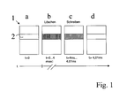
- Fig.1 schematically shows a flash memory 1 with a plurality of memory pages, one of which by means of a write command (write command) to be described memory page 2 is highlighted.
- a write command (write command) to be described memory page 2 is highlighted.
- the flash memory Before the arrival of the write command to the flash memory 1, ie in a time interval t ⁇ 0, the flash memory is in any written or erased state, see.
Landscapes
- Techniques For Improving Reliability Of Storages (AREA)
- Storage Device Security (AREA)
Abstract
Description
- Die Erfindung betrifft ein Verfahren zur Fehleranalyse an einem in Speicherbereiche unterteilten elektronischen Speicher, insbesondere zum Erkennen von fälschlicherweise gelöschten Speicherbereichen in dem Speicher, z.B. einem in Speicherseiten (Pages) unterteilten Flash-Speicher.
- Moderne Chipkarten benutzen für Betriebssystem und Daten Flash-Speicher. Flash-Speicher sind in Speicherseiten (Pages) unterteilt, die zurzeit eine typische Größe von 256 Bytes, d.h. 256*8 einzelnen Speicherzellen, haben. Die Chipkarte hat neben dem Flash-Speicher insbesondere eine Prozessor und einen Arbeitsspeicher RAM.
- Jede Speicherzelle des Flash-Speichers kann zwei Speicherzustände annehmen, beschrieben und gelöscht. Ein byteweises (ggf. auch bit- oder wortweises) Ansteuern des Flash-Speichers ist nur beim Schreiben, d.h. beim Programmieren des Speichers in den beschriebenen Zustand, möglich. Beim Löschen, d.h. beim Programmieren des Flash-Speichers in den gelöschten Zustand, ist der Flash-Speicher nur seitenweise ansteuerbar.
- Ein Schreibkommando, das z.B. durch ein Chipkartenbetriebssystem an den Speicher gesandt wird, wird daher im Speicher umgesetzt in zwei Programmierschritte, nämlich einen zuerst durchgeführten Löschvorgang und einen anschließenden Schreibvorgang. Beim Löschvorgang wird die gesamte Speicherseite, auf der die zu beschreibenden Speicherzellen / Bytes angeordnet sind, in einen Pufferspeicher kopiert und anschließend gelöscht. Beim Schreibvorgang werden die im Schreibkommando angegebenen Speicherzellen in den beschriebenen Speicherzustand programmiert. Bei einem atomaren Schreibvorgang, der vor allem für wichtige Speicherinhalte gewählt wird, wird als Pufferspeicher für die zu löschende Speicherseite eine andere Speicherseite im nichtflüchtigen aber langsamen Flash-Speicher verwendet.
- Vor allem für weniger wichtige Speicherinhalte oder zeitkritische Programmiervorgänge werden nichtatomare Schreibvorgänge gewählt, bei denen als Pufferspeicher für die zu löschende Speicherseite ein Speicherbereich im schnellen aber flüchtigen Arbeitsspeicher RAM verwendet wird.
- Tritt während der Abarbeitung eines nichtatomaren Schreibkommandos für eine Speicherseite während des Löschvorgang oder danach eine Störung, z.B. Unterbrechung in der Spannungsversorgung oder Spannungsabfall, auf, bevor der im Schreibkommando enthaltene Schreibvorgang durchgeführt worden ist, ist der ursprüngliche Speicherinhalt der Speicherseite verloren, da die Pufferung der Speicherseite ja im flüchtigen Speicher erfolgte. Datenverluste in einem Speicher durch Spannungsunterbrechungen oder Spannungsabfälle unter ein zum Erhalt des Speicherinhalts erforderliches Spannungsniveau werden mitunter auch als Tearprobleme bezeichnet.
- Das Fehlen des Speicherinhalts der gelöschten und nicht wiederbeschriebenen Speicherseite kann Datenverlust bedeuten oder aber auch die Funktionsfähigkeit des Speichers beeinträchtigen, insbesondere falls Teile eines im Flash-Speicher abgespeicherten Betriebssystems gelöscht wurden. Gerade in Chipkarten, wo der Flash-Speicher knapp bemessen ist, kommt es vor, dass im Flash-Speicher zum Teil auf einer einzigen Speicherseite sowohl Daten, die häufiger geändert werden, als auch Teile des Betriebssystems abgespeichert sind. Jede Datenänderung mittels eines nichtatomaren Schreibkommandos kann somit das Betriebssystem gefährden und damit nicht nur den Speicher selbst, sondern auch weitere Komponenten der Chipkarte.
- Fällt das Betriebssystem einer Chipkarte mit Flash-Speicher aus, oder sind in einer solchen Chipkarte Daten nicht mehr auffindbar, kann dies andererseits die unterschiedlichsten Gründe haben. Dem Nutzer der Chipkarte wäre schon damit geholfen, könnte er verifizieren, dass die Chipkartenprobleme auf fälschlich gelöschte Speicherseiten im Flash-Speicher zurückgehen.
- Ein direkter lesender Zugriff auf den Flash-Speicher einer Chipkarte von außerhalb der Chipkarte ist nach der Ausgabe der Chipkarte aus Sicherheitsgründen nicht mehr möglich. Somit ist der Flash-Speicher nicht direkt auf fälschlich gelöschte Speicherseiten hin überprüfbar.
- Der Erfindung liegt die Aufgabe zu Grunde, ein Verfahren zur Fehleranalyse an einem in Speicherbereiche unterteilten elektronischen Speicher, insbesondere zum Erkennen von fälschlicherweise gelöschten Speicherbereichen in dem Speicher, z.B. einem in Speicherseiten (Pages) unterteilten Flash-Speicher, zu schaffen.
- Die Aufgabe wird gelöst durch ein Verfahren nach Anspruch 1. Vorteilhafte Ausgestaltungen der Erfindung sind in den abhängigen Ansprüchen angegeben.
- Das Verfahren nach Anspruch 1 ist zum Erkennen von fälschlicherweise gelöschten Speicherbereichen in einem in Speicherbereiche unterteilten elektronischen Speicher eingerichtet und ist gekennzeichnet durch die Schritte
- a) Ermitteln einer Soll-Anzahl von gelöschten Speicherbereichen,
- b) Ermitteln einer Ist-Anzahl von gelöschten Speicherbereichen,
- c) Vergleichen der Ist-Anzahl und der Soll-Anzahl miteinander, und
- d) im Fall, dass die Ist-Anzahl und die Soll-Anzahl unterschiedlich sind, Erkennen, dass fälschlicherweise gelöschte Speicherbereiche existieren.
- Anhand jeder erkannten Abweichung der Ist-Anzahl von gelöschten Speicherbereichen von der Soll-Anzahl von gelöschten Speicherbereichen ist erkennbar bzw. wird definiert, dass Speicherbereiche existieren müssen, die fälschlicherweise gelöscht sind.
- Identifiziert ein Programmierer bei einem funktionsunfähigen oder fehlfunktionierenden Speicher solche fälschlicherweise gelöschten Speicherseiten, so kann er zumindest andere Fehlerursachen ausschließen und möglicherweise die verlorengegangenen Speicherinhalte rekonstruieren und somit den Speicher bzw. seine Speicherinhalte wieder funktionsfähig machen.
- Daher ist gemäß Anspruch 1 ein Verfahren zur Fehleranalyse an einem in Speicherbereiche unterteilten elektronischen Speicher, insbesondere zum Erkennen von fälschlicherweise gelöschten Speicherbereichen in dem Speicher, geschaffen.
- Wahlweise werden die Ist-Anzahl und die Soll-Anzahl - und ggf. die Identifizierungszeichen, vgl. weiter unten - an ein zur Kommunikation mit dem Speicher eingerichtetes Terminal bereitgestellt, beispielsweise bei einem Speicher in einer Chipkarte an ein Chipkartenterminal. Wahlweise wird das Vergleichen der Ist-Anzahl und der Soll-Anzahl im Terminal durchgeführt.
- Wahlweise ist als Speicher ein Speicher vorgesehen, bei dem jedes Schreibkommando (Schreibbefehl) einen zuerst durchgeführten Löschvorgang und einen nachfolgenden Schreibvorgang umfasst. Wahlweise ist jeder Speicherbereich in Speicherzellen unterteilt, die wahlweise wiederum zu Bytes oder Worten innerhalb des Speicherbereichs gruppiert sind. Wahlweise kann bei einem Löschvorgang stets nur ein ganzer Speicherbereich gelöscht werden, nicht jedoch einzelne Speicherzellen, Bytes oder Worte. Wahlweise können bei einem Schreibvorgang einzelne Speicherzellen oder Bytes oder Worte beschrieben werden.
- Wahlweise ist der Speicher ein Flash-Speicher und sind die Speicherbereiche Speicherseiten in dem Flash-Speicher. Der Flash-Speicher hat die im vorangehenden Absatz beschriebenen Eigenschaften.
- Der Schritt b) Ermitteln einer Ist-Anzahl von gelöschten Speicherbereichen wird wahlweise durchgeführt als Zählen von Speicherbereichen mit einem Speicherinhalt entsprechend einem gelöschten Zustand des jeweiligen Speicherbereichs.
- Ein typischer Löschvorgang in einem Flash-Speicher dauert vier Millisekunden und somit relativ lange. Ein typischer Schreibvorgang in einem Flash-Speicher dauert ungefähr zehn Mikrosekunden und somit relativ kurz. In den meisten Fällen ist daher nach einer Spannungsunterbrechung während eines nichtatomaren Schreibkommandos auf eine Speicherseite die Speicherseite im Flash-Speicher gelöscht, genauer fälschlicherweise gelöscht, hat also einen gelöschten Speicherzustand. Die Wahrscheinlichkeit, dass der Spannungsabbruch während des Schreibvorgangs auftritt, ist auf Grund der kurzen Zeitdauer des Schreibvorgangs gering. Somit ist auch die Wahrscheinlichkeit gering, dass nach einer Spannungsunterbrechung die Speicherseite teilweise beschrieben ist.
- Der Schritt a) Ermitteln einer Soll-Anzahl von gelöschten Speicherbereichen wird wahlweise durchgeführt als Festsetzen der Soll-Anzahl von gelöschten Speicherbereichen auf Null.
- Das vorstehende Ausführungsbeispiel wird anhand einer Chipkarte mit einem in Speicherseiten aufgeteilten Flash-Speicher erläutert. In Chipkarten ist in der Regel der verfügbare Flash-Speicher knapp bemessen. Daher ist der Flash-Speicher in der Regel voll und hat im intakten Zustand keine leeren Speicherseiten. Somit ist die Soll-Anzahl von gelöschten Speicherseiten im Flash-Speicher einer solchen Chipkarte Null. Ist die gemäß Schritt b) ermittelte Ist-Anzahl von gelöschten Speicherseiten ungleich Null, so bedeutet dies, dass fälschlicherweise gelöschte Speicherseiten existieren, d.h. Speicherseiten, die eigentlich beschrieben sein sollten. Für andere in Speicherbereiche unterteilte Speicher gilt das Gesagte analog.
- Wahlweise wird der Schritt a) Ermitteln einer Soll-Anzahl von gelöschten Speicherbereichen durchgeführt als Ermitteln einer Anzahl von zuvor durchgeführten Löschbefehlen (Löschkommandos). Gelöschte Speicherbereiche können durch einen Löschbefehl erzeugt werden. Bei einem Löschbefehl wird ein Löschvorgang an einem Speicherbereich durchgeführt, ohne dass nachfolgend ein Schreibvorgang durchgeführt wird. Somit wird mit jedem Löschbefehl ein leerer oder gelöschter Speicherbereich erzeugt. Gibt es in dem Speicher mehr gelöschte Bereiche als Löschbefehle durchgeführt wurden, dann existieren fälschlicherweise gelöschte Speicherbereiche. Diese Variante der Erfindung ist auch für Chipkarten anwendbar, bei denen absichtlich Speicherbereiche bzw. Speicherseiten gelöscht worden sind.
- Wahlweise ist jedem Speicherbereich ein Identifizierungszeichen zugeordnet, und das Verfahren umfasst den weiteren Schritt e) Ermitteln der Identifizierungszeichen der im Schritt b) ermittelten gelöschten Speicherbereiche.
- Als Identifizierungszeichen können beispielsweise Nummern von Speicherbereichen vorgesehen sein, beispielsweise Seitennummern von Speicherseiten in einem Flash-Speicher.
- Anhand der Identifizierungszeichen der gelöschten Speicherbereiche ist erkennbar, welche Speicherbereiche (z.B. Speicherseiten) fälschlicherweise gelöscht worden sind. Somit ist - zumindest für den Programmierer des Speichers - erkennbar, welche Speicherinhalte gelöscht worden sind. Wurden beispielsweise bestimmte Daten gelöscht, so kann der Programmierer versuchen, diese Daten erneut in den Speicher einzuprogrammieren. Wurden Programmteile oder Teile des Betriebssystems gelöscht, so ist zumindest erkennbar, dass andere Fehlerquellen höchstwahrscheinlich ausscheiden, und möglicherweise ist die Wiederherstellung des Programms oder Betriebssystems durch erneute Einprogrammierung der fälschlicherweise gelöschten Teile in den Speicher oder als Patch in einen angebunden Speicher möglich.
- Wahlweise ist der Speicher zur Ansteuerung durch ein Chipkartenbetriebssystem eingerichtet, das z.B. zumindest teilweise oder aber auch ganz im Speicher abgespeichert ist, und wobei die Ist-Anzahl und die Soll-Anzahl und ggf. die Identifizierungszeichen mittels zumindest eines an den Speicher gesendeten Chipkarten-Kommandos ermittelt werden. Wahlweise werden die Chipkarten-Kommandos durch ein Chipkartenterminal gesendet. Wahlweise werden die Ist-Anzahl und die Soll-Anzahl jeweils mittels eines Zählers gezählt und wird mittels des Chipkarten-Kommandos der Zählerstand eines oder beider der Zähler ausgelesen.
- Wahlweise wird als das zumindest eine Chipkarten-Kommando zumindest ein Kommando zum Auslesen der Ist-Anzahl, der Soll-Anzahl und ggf. der Identifizierungszeichen an den Speicher gesendet, und wobei in Reaktion auf das zumindest eine Chipkarten-Kommando eine Antwort mit der Ist-Anzahl (z.B. Zählerstand) und der Soll-Anzahl (z.B. Zählerstand) und ggf. dem oder den Identifizierungszeichen bereitgestellt wird. Für diese Variante der Erfindung, bei der die Ist-Anzahl, die Soll-Anzahl und ggf. das oder die Identifizierungszeichen mittels eines Lesekommandos gewonnen werden, ist die Funktionsfähigkeit des Betriebssystems, durch welches der Speicher angesteuert wird, zwingend erforderlich.
- Wahlweise wird als das zumindest eine Chipkarten-Kommando ein Reset-Kommando an den Speicher gesendet (z.B. durch ein Chipkartenterminal), und wobei in Reaktion auf das Reset-Kommando (Rücksetz-Kommando) in einem Answer-To-Reset-Kommando (ATR-Kommando) die Ist-Anzahl und die Soll-Anzahl und ggf. die Identifizierungszeichen bereitgestellt werden (z.B. an das Chipkartenterminal). Diese Variante der Erfindung, bei der die Ist-Anzahl, die Soll-Anzahl und ggf. das oder die Identifizierungszeichen mittels eines Reset-Kommandos und eines daraufhin gesendeten ATR-Kommandos gewonnen werden, ist die Funktionsfähigkeit des Betriebssystems, durch welches der Speicher angesteuert wird, nicht erforderlich. Mit anderen Worten können selbst aus einem Speichersystem, z.B. einer Chipkarte mit einem Prozessor und dem Speicher, bei dem das Betriebssystem beeinträchtigt ist, die Ist-Anzahl und die Soll-Anzahl und ggf. die Identifizierungszeichen mittels der für z.B. Chipkarten standardmäßig vorgesehenen Kommandofolge Reset, Answer-To-Reset ermittelt werden. Bei Speichersystemen mit funktionsfähigem Betriebssystem für den Speicher ist die Ermittlung von Ist-Anzahl, Soll-Anzahl und ggf. Identifizierungszeichen über die Kommandofolge Reset, Answer-To-Reset natürlich ebenso möglich.
- Wahlweise ist in dem Speicher ein Chipkarten-Betriebssystem, oder zumindest ein Teil davon, abgespeichert, und wobei der Speicher in ein Prozessorsystem implementiert ist. Als Prozessorsystem ist beispielsweise eine Chipkarte (Smart Card) mit Mikroprozessor und Flash-Speicher vorgesehen, oder ein funktional vergleichbar wie eine Chipkarte aufgebauter Token in beliebiger Bauform, z.B. wie bei einem Speicher-Stick oder dergleichen.
- Im Folgenden wird die Erfindung an Hand von Ausführungsbeispielen und unter Bezugnahme auf die Zeichnung näher erläutert, in der zeigt:
-
Fig.1 einen für die Erfindung geeigneten Flash-Speicher. -
Fig.1 zeigt schematisch einen Flash-Speicher 1 mit einer Mehrzahl von Speicherseiten, von denen eine mittels eines Schreibkommandos (Schreibbefehls) zu beschreibende Speicherseite 2 hervorgehoben ist. Vor dem Eintreffen des Schreibkommandos beim Flash-Speicher 1, d.h. in einem Zeitintervall t<0, befindet sich der Flash-Speicher in einem beliebigen beschriebenen oder gelöschten Zustand, vgl. Teilfigur a. Zum Zeitpunkt t=0 geht ein Schreibkommando beim Flash-Speicher 1 ein. Im vier Millisekunden langen Zeitintervall von t=0 bis t=4ms (vier Millisekunden) wird die gesamte Speicherseite 2 gelöscht, vgl. Teilfigur b. Im 10 Mikrosekunden langen Zeitintervall von t=4ms bis t=4,01ms werden einzelne Speicherzellen der Speicherseite 2 beschrieben, entsprechend den Angaben im Schreibkommando, vgl. Teilfigur c. Nach Ablauf der 10 Mikrosekunden dauernden Schreibdauer ist der Flash-Speicher 2 in einem neu beschriebenen Zustand, vgl. Teilfigur d.
Claims (10)
- Verfahren zum Erkennen von fälschlicherweise gelöschten Speicherbereichen (2) in einem in Speicherbereiche (2) unterteilten elektronischen Speicher (1), gekennzeichnet durch die Schrittea) Ermitteln einer Soll-Anzahl von gelöschten Speicherbereichen (2),b) Ermitteln einer Ist-Anzahl von gelöschten Speicherbereichen (2),c) Vergleichen der Ist-Anzahl und der Soll-Anzahl miteinander, undd) im Fall, dass die Ist-Anzahl und die Soll-Anzahl unterschiedlich sind, Erkennen, dass fälschlicherweise gelöschte Speicherbereiche (2) existieren.
- Verfahren nach Anspruch 1, wobei der Speicher (1) ein Flash-Speicher ist und die Speicherbereiche (2) Speicherseiten in dem Flash-Speicher sind.
- Verfahren nach Anspruch 1 oder 2, wobei der Schritt b) Ermitteln einer Ist-Anzahl von gelöschten Speicherbereichen (2) durchgeführt wird als Zählen von Speicherbereichen (2) mit einem Speicherinhalt entsprechend einem gelöschten Zustand des jeweiligen Speicherbereichs (2).
- Verfahren nach einem der Ansprüche 1 bis 3, wobei der Schritt a) Ermitteln einer Soll-Anzahl von gelöschten Speicherbereichen (2) durchgeführt wird als Festsetzen der Soll-Anzahl von gelöschten Speicherbereichen (2) auf Null.
- Verfahren nach einem der Ansprüche 1 bis 3, wobei der Schritt a) Ermitteln einer Soll-Anzahl von gelöschten Speicherbereichen (2) durchgeführt wird als Ermitteln einer Anzahl von zuvor durchgeführten Löschbefehlen.
- Verfahren nach einem der Ansprüche 1 bis 5, wobei jedem Speicherbereich (2) ein Identifizierungszeichen zugeordnet ist, und mit dem weiteren Schritt e) Ermitteln der Identifizierungszeichen der im Schritt b) ermittelten gelöschten Speicherbereiche (2).
- Verfahren nach einem der Ansprüche 1 bis 6, wobei der Speicher (1) zur Ansteuerung durch ein Chipkartenbetriebssystem eingerichtet ist, und wobei die Ist-Anzahl und die Soll-Anzahl und ggf. die Identifizierungszeichen mittels zumindest eines an den Speicher (1) gesendeten Chipkarten-Kommandos ermittelt werden.
- Verfahren nach Anspruch 7, wobei als das zumindest eine Chipkarten-Kommando zumindest ein Kommando zum Auslesen der Ist-Anzahl, der Soll-Anzahl und ggf. der Identifizierungszeichen an den Speicher (1) gesendet wird, und wobei in Reaktion auf das zumindest eine Chipkarten-Kommando die Ist-Anzahl und die Soll-Anzahl und ggf. die Identifizierungszeichen bereitgestellt werden.
- Verfahren nach Anspruch 7, wobei als das zumindest eine Chipkarten-Kommando ein Reset-Kommando an den Speicher (1) gesendet wird, und wobei in Reaktion auf das Reset-Kommando in einem Answer-To-Reset-Kommando die Ist-Anzahl und die Soll-Anzahl und ggf. die Identifizierungszeichen bereitgestellt werden.
- Verfahren nach einem der Ansprüche 1 bis 9, wobei in dem Speicher (1) ein Chipkarten-Betriebssystem, oder zumindest ein Teil davon, abgespeichert ist, und wobei der Speicher (1) in ein Prozessorsystem, insbesondere eine Chipkarte oder ein funktional vergleichbar wie eine Chipkarte aufgebautes Token, implementiert ist, das zumindest einen Mikroprozessor und den Speicher (1) aufweist.
Applications Claiming Priority (1)
| Application Number | Priority Date | Filing Date | Title |
|---|---|---|---|
| DE201110107435 DE102011107435A1 (de) | 2011-07-15 | 2011-07-15 | Verfahren zum Erkennen von gelöschten Speicherbereichen |
Publications (2)
| Publication Number | Publication Date |
|---|---|
| EP2546837A1 true EP2546837A1 (de) | 2013-01-16 |
| EP2546837B1 EP2546837B1 (de) | 2016-12-21 |
Family
ID=46027529
Family Applications (1)
| Application Number | Title | Priority Date | Filing Date |
|---|---|---|---|
| EP12002829.5A Not-in-force EP2546837B1 (de) | 2011-07-15 | 2012-04-23 | Verfahren zum Erkennen von gelöschten Speicherbereichen |
Country Status (2)
| Country | Link |
|---|---|
| EP (1) | EP2546837B1 (de) |
| DE (1) | DE102011107435A1 (de) |
Citations (4)
| Publication number | Priority date | Publication date | Assignee | Title |
|---|---|---|---|---|
| WO2008045839A1 (en) * | 2006-10-12 | 2008-04-17 | Sandisk Corporation | Non-volatile memory with worst-case control data management and methods therefor |
| US20090067241A1 (en) * | 2007-09-12 | 2009-03-12 | Gorobets Sergey A | Data protection for write abort |
| US20100169586A1 (en) * | 2008-12-31 | 2010-07-01 | Li-Pin Chang | Memory storage device and a control method thereof |
| US20110153913A1 (en) * | 2009-12-18 | 2011-06-23 | Jianmin Huang | Non-Volatile Memory with Multi-Gear Control Using On-Chip Folding of Data |
Family Cites Families (5)
| Publication number | Priority date | Publication date | Assignee | Title |
|---|---|---|---|---|
| DE19911794B4 (de) * | 1999-03-17 | 2005-10-06 | Robert Bosch Gmbh | Verfahren und Vorrichtung zur Absicherung bei Veränderung des Speicherinhalts von Steuergeräten |
| DE102004005290B3 (de) * | 2004-02-03 | 2005-07-21 | Giesecke & Devrient Gmbh | Verfahren und Vorrichtung zur Absicherung von Daten in einem nichtflüchtigen Datenspeicher |
| JP4999325B2 (ja) * | 2005-12-21 | 2012-08-15 | ルネサスエレクトロニクス株式会社 | フラッシュメモリ |
| US20080320253A1 (en) * | 2007-06-19 | 2008-12-25 | Andrew Tomlin | Memory device with circuitry for writing data of an atomic transaction |
| DE102009048144A1 (de) * | 2009-10-02 | 2011-04-07 | Giesecke & Devrient Gmbh | Verfahren zum Schreiben von Datensätzen in einen nicht-flüchtigen Datenspeicher |
-
2011
- 2011-07-15 DE DE201110107435 patent/DE102011107435A1/de not_active Withdrawn
-
2012
- 2012-04-23 EP EP12002829.5A patent/EP2546837B1/de not_active Not-in-force
Patent Citations (4)
| Publication number | Priority date | Publication date | Assignee | Title |
|---|---|---|---|---|
| WO2008045839A1 (en) * | 2006-10-12 | 2008-04-17 | Sandisk Corporation | Non-volatile memory with worst-case control data management and methods therefor |
| US20090067241A1 (en) * | 2007-09-12 | 2009-03-12 | Gorobets Sergey A | Data protection for write abort |
| US20100169586A1 (en) * | 2008-12-31 | 2010-07-01 | Li-Pin Chang | Memory storage device and a control method thereof |
| US20110153913A1 (en) * | 2009-12-18 | 2011-06-23 | Jianmin Huang | Non-Volatile Memory with Multi-Gear Control Using On-Chip Folding of Data |
Also Published As
| Publication number | Publication date |
|---|---|
| DE102011107435A1 (de) | 2013-01-17 |
| EP2546837B1 (de) | 2016-12-21 |
Similar Documents
| Publication | Publication Date | Title |
|---|---|---|
| EP0067364B1 (de) | Verfahren und Anordnung zum nichtflüchtigen Speichern des Zählerstandes einer elektronischen Zählschaltung | |
| EP1850897B1 (de) | Inhalationstherapievorrichtung und verfahren zu deren betrieb | |
| DE102009051862A1 (de) | Speichervorrichtung und Speicherverfahren | |
| DE102022004036A1 (de) | Verfahren zur Verwaltung eines Datenspeichersystems für Fahrzeuge und Datenspeicherverwaltungsvorrichtung | |
| DE102018123978A1 (de) | Verfahren und vorrichtung zur speichercontrollererkennung von anbieterspezifischen nichtflüchtigen speichergeräten | |
| DE69327924T2 (de) | Verfahren zur automatischen Initialisierung eines Mikroprozessorsystems und entsprechendes System | |
| EP1037140B1 (de) | Verfahren und Vorrichtung zur Absicherung bei Veränderung des Speicherinhalts von Steuergeräten | |
| DE19931184A1 (de) | Verfahren und Vorrichtung zur Veränderung des Speicherinhalts von Steuergeräten | |
| DE60224937T2 (de) | Verfahren und anordnung zum verknüpfen von verwandelten appletdateien | |
| EP2546837B1 (de) | Verfahren zum Erkennen von gelöschten Speicherbereichen | |
| DE10002203A1 (de) | Verfharen zum Schutz eines Mikrorechner-Systems gegen Manipulation von in einer Speicheranordnung des Mikrorechner-Systems gespeicherten Daten | |
| DE102010054446A1 (de) | Portabler Datenträger mit Fehlbedienungszähler | |
| DE102006009214B4 (de) | Verfahren und Vorrichtung zum Schreiben in eine Zielspeicherseite eines Speichers | |
| DE102009055390A1 (de) | Vorrichtung und Verfahren zum Schreiben von Daten, die zu speichern sind, in einen vorbestimmten Speicherbereich | |
| EP1625592B1 (de) | Vorrichtung und verfahren zum behandeln eines zustands eines speichers | |
| EP1892639B1 (de) | Sichere Programmcodeausführung | |
| DE10030990A1 (de) | Verfahren zum Beschreiben und Löschen eines nichtflüchtigen Speicherbereichs | |
| EP2002446B1 (de) | Verfahren zum betreiben einer speichereinrichtung mit markierung von als fehlerhaft erkannten speicherblöcken | |
| EP0214390A1 (de) | Freigabeverfahren für einen zugriffskontrollierten Anwenderspeicher und Anordnung zur Durchführung des Verfahrens | |
| EP1564754B1 (de) | Verfahren und Vorrichtung zur Verwaltung von Daten in einem nichtflüchtigen Datenspeicher | |
| DE10328238B4 (de) | Verfahren zum Laden von Chipkarten mit Initialisierungs- und/oder Personalisierungsdaten | |
| DE102004006308B4 (de) | Verfahren zum Verändern von Programmcode eines tragbaren Datenträgers mittels Patchdaten | |
| EP2012280A2 (de) | Tragbarer Datenträger und Verfahren zur Personalisierung eines tragbaren Datenträgers | |
| DE102016212956B4 (de) | Verfahren zum Betreiben eines seriellen nicht-flüchtigen Halbleiterspeichers | |
| DE102017010430B4 (de) | Verfahren zum Bewahren von Flashspeicher durch sequenzielle Belegung durch Einmalcode-Module |
Legal Events
| Date | Code | Title | Description |
|---|---|---|---|
| PUAI | Public reference made under article 153(3) epc to a published international application that has entered the european phase |
Free format text: ORIGINAL CODE: 0009012 |
|
| AK | Designated contracting states |
Kind code of ref document: A1 Designated state(s): AL AT BE BG CH CY CZ DE DK EE ES FI FR GB GR HR HU IE IS IT LI LT LU LV MC MK MT NL NO PL PT RO RS SE SI SK SM TR |
|
| AX | Request for extension of the european patent |
Extension state: BA ME |
|
| 17P | Request for examination filed |
Effective date: 20130612 |
|
| RBV | Designated contracting states (corrected) |
Designated state(s): AL AT BE BG CH CY CZ DE DK EE ES FI FR GB GR HR HU IE IS IT LI LT LU LV MC MK MT NL NO PL PT RO RS SE SI SK SM TR |
|
| 17Q | First examination report despatched |
Effective date: 20141105 |
|
| GRAP | Despatch of communication of intention to grant a patent |
Free format text: ORIGINAL CODE: EPIDOSNIGR1 |
|
| RIC1 | Information provided on ipc code assigned before grant |
Ipc: G06F 12/02 20060101ALI20160624BHEP Ipc: G06F 11/00 20060101ALI20160624BHEP Ipc: G11C 16/14 20060101AFI20160624BHEP |
|
| INTG | Intention to grant announced |
Effective date: 20160713 |
|
| GRAS | Grant fee paid |
Free format text: ORIGINAL CODE: EPIDOSNIGR3 |
|
| GRAA | (expected) grant |
Free format text: ORIGINAL CODE: 0009210 |
|
| AK | Designated contracting states |
Kind code of ref document: B1 Designated state(s): AL AT BE BG CH CY CZ DE DK EE ES FI FR GB GR HR HU IE IS IT LI LT LU LV MC MK MT NL NO PL PT RO RS SE SI SK SM TR |
|
| REG | Reference to a national code |
Ref country code: GB Ref legal event code: FG4D Free format text: NOT ENGLISH |
|
| REG | Reference to a national code |
Ref country code: CH Ref legal event code: EP |
|
| REG | Reference to a national code |
Ref country code: IE Ref legal event code: FG4D Free format text: LANGUAGE OF EP DOCUMENT: GERMAN |
|
| REG | Reference to a national code |
Ref country code: AT Ref legal event code: REF Ref document number: 856111 Country of ref document: AT Kind code of ref document: T Effective date: 20170115 |
|
| REG | Reference to a national code |
Ref country code: DE Ref legal event code: R096 Ref document number: 502012009056 Country of ref document: DE |
|
| PG25 | Lapsed in a contracting state [announced via postgrant information from national office to epo] |
Ref country code: LV Free format text: LAPSE BECAUSE OF FAILURE TO SUBMIT A TRANSLATION OF THE DESCRIPTION OR TO PAY THE FEE WITHIN THE PRESCRIBED TIME-LIMIT Effective date: 20161221 |
|
| REG | Reference to a national code |
Ref country code: FR Ref legal event code: PLFP Year of fee payment: 6 |
|
| REG | Reference to a national code |
Ref country code: LT Ref legal event code: MG4D |
|
| REG | Reference to a national code |
Ref country code: NL Ref legal event code: MP Effective date: 20161221 |
|
| PG25 | Lapsed in a contracting state [announced via postgrant information from national office to epo] |
Ref country code: GR Free format text: LAPSE BECAUSE OF FAILURE TO SUBMIT A TRANSLATION OF THE DESCRIPTION OR TO PAY THE FEE WITHIN THE PRESCRIBED TIME-LIMIT Effective date: 20170322 Ref country code: NO Free format text: LAPSE BECAUSE OF FAILURE TO SUBMIT A TRANSLATION OF THE DESCRIPTION OR TO PAY THE FEE WITHIN THE PRESCRIBED TIME-LIMIT Effective date: 20170321 Ref country code: SE Free format text: LAPSE BECAUSE OF FAILURE TO SUBMIT A TRANSLATION OF THE DESCRIPTION OR TO PAY THE FEE WITHIN THE PRESCRIBED TIME-LIMIT Effective date: 20161221 Ref country code: LT Free format text: LAPSE BECAUSE OF FAILURE TO SUBMIT A TRANSLATION OF THE DESCRIPTION OR TO PAY THE FEE WITHIN THE PRESCRIBED TIME-LIMIT Effective date: 20161221 |
|
| PG25 | Lapsed in a contracting state [announced via postgrant information from national office to epo] |
Ref country code: HR Free format text: LAPSE BECAUSE OF FAILURE TO SUBMIT A TRANSLATION OF THE DESCRIPTION OR TO PAY THE FEE WITHIN THE PRESCRIBED TIME-LIMIT Effective date: 20161221 Ref country code: FI Free format text: LAPSE BECAUSE OF FAILURE TO SUBMIT A TRANSLATION OF THE DESCRIPTION OR TO PAY THE FEE WITHIN THE PRESCRIBED TIME-LIMIT Effective date: 20161221 Ref country code: RS Free format text: LAPSE BECAUSE OF FAILURE TO SUBMIT A TRANSLATION OF THE DESCRIPTION OR TO PAY THE FEE WITHIN THE PRESCRIBED TIME-LIMIT Effective date: 20161221 |
|
| PG25 | Lapsed in a contracting state [announced via postgrant information from national office to epo] |
Ref country code: NL Free format text: LAPSE BECAUSE OF FAILURE TO SUBMIT A TRANSLATION OF THE DESCRIPTION OR TO PAY THE FEE WITHIN THE PRESCRIBED TIME-LIMIT Effective date: 20161221 |
|
| REG | Reference to a national code |
Ref country code: DE Ref legal event code: R081 Ref document number: 502012009056 Country of ref document: DE Owner name: GIESECKE+DEVRIENT MOBILE SECURITY GMBH, DE Free format text: FORMER OWNER: GIESECKE & DEVRIENT GMBH, 81677 MUENCHEN, DE |
|
| PG25 | Lapsed in a contracting state [announced via postgrant information from national office to epo] |
Ref country code: IS Free format text: LAPSE BECAUSE OF FAILURE TO SUBMIT A TRANSLATION OF THE DESCRIPTION OR TO PAY THE FEE WITHIN THE PRESCRIBED TIME-LIMIT Effective date: 20170421 Ref country code: SK Free format text: LAPSE BECAUSE OF FAILURE TO SUBMIT A TRANSLATION OF THE DESCRIPTION OR TO PAY THE FEE WITHIN THE PRESCRIBED TIME-LIMIT Effective date: 20161221 Ref country code: RO Free format text: LAPSE BECAUSE OF FAILURE TO SUBMIT A TRANSLATION OF THE DESCRIPTION OR TO PAY THE FEE WITHIN THE PRESCRIBED TIME-LIMIT Effective date: 20161221 Ref country code: EE Free format text: LAPSE BECAUSE OF FAILURE TO SUBMIT A TRANSLATION OF THE DESCRIPTION OR TO PAY THE FEE WITHIN THE PRESCRIBED TIME-LIMIT Effective date: 20161221 Ref country code: CZ Free format text: LAPSE BECAUSE OF FAILURE TO SUBMIT A TRANSLATION OF THE DESCRIPTION OR TO PAY THE FEE WITHIN THE PRESCRIBED TIME-LIMIT Effective date: 20161221 |
|
| RAP2 | Party data changed (patent owner data changed or rights of a patent transferred) |
Owner name: GIESECKE+DEVRIENT MOBILE SECURITY GMBH |
|
| PG25 | Lapsed in a contracting state [announced via postgrant information from national office to epo] |
Ref country code: BG Free format text: LAPSE BECAUSE OF FAILURE TO SUBMIT A TRANSLATION OF THE DESCRIPTION OR TO PAY THE FEE WITHIN THE PRESCRIBED TIME-LIMIT Effective date: 20170321 Ref country code: PL Free format text: LAPSE BECAUSE OF FAILURE TO SUBMIT A TRANSLATION OF THE DESCRIPTION OR TO PAY THE FEE WITHIN THE PRESCRIBED TIME-LIMIT Effective date: 20161221 Ref country code: SM Free format text: LAPSE BECAUSE OF FAILURE TO SUBMIT A TRANSLATION OF THE DESCRIPTION OR TO PAY THE FEE WITHIN THE PRESCRIBED TIME-LIMIT Effective date: 20161221 Ref country code: PT Free format text: LAPSE BECAUSE OF FAILURE TO SUBMIT A TRANSLATION OF THE DESCRIPTION OR TO PAY THE FEE WITHIN THE PRESCRIBED TIME-LIMIT Effective date: 20170421 Ref country code: IT Free format text: LAPSE BECAUSE OF FAILURE TO SUBMIT A TRANSLATION OF THE DESCRIPTION OR TO PAY THE FEE WITHIN THE PRESCRIBED TIME-LIMIT Effective date: 20161221 Ref country code: ES Free format text: LAPSE BECAUSE OF FAILURE TO SUBMIT A TRANSLATION OF THE DESCRIPTION OR TO PAY THE FEE WITHIN THE PRESCRIBED TIME-LIMIT Effective date: 20161221 |
|
| REG | Reference to a national code |
Ref country code: DE Ref legal event code: R097 Ref document number: 502012009056 Country of ref document: DE |
|
| PLBE | No opposition filed within time limit |
Free format text: ORIGINAL CODE: 0009261 |
|
| STAA | Information on the status of an ep patent application or granted ep patent |
Free format text: STATUS: NO OPPOSITION FILED WITHIN TIME LIMIT |
|
| 26N | No opposition filed |
Effective date: 20170922 |
|
| PG25 | Lapsed in a contracting state [announced via postgrant information from national office to epo] |
Ref country code: DK Free format text: LAPSE BECAUSE OF FAILURE TO SUBMIT A TRANSLATION OF THE DESCRIPTION OR TO PAY THE FEE WITHIN THE PRESCRIBED TIME-LIMIT Effective date: 20161221 |
|
| REG | Reference to a national code |
Ref country code: CH Ref legal event code: PL |
|
| GBPC | Gb: european patent ceased through non-payment of renewal fee |
Effective date: 20170423 |
|
| REG | Reference to a national code |
Ref country code: IE Ref legal event code: MM4A |
|
| PG25 | Lapsed in a contracting state [announced via postgrant information from national office to epo] |
Ref country code: MC Free format text: LAPSE BECAUSE OF FAILURE TO SUBMIT A TRANSLATION OF THE DESCRIPTION OR TO PAY THE FEE WITHIN THE PRESCRIBED TIME-LIMIT Effective date: 20161221 |
|
| PG25 | Lapsed in a contracting state [announced via postgrant information from national office to epo] |
Ref country code: SI Free format text: LAPSE BECAUSE OF FAILURE TO SUBMIT A TRANSLATION OF THE DESCRIPTION OR TO PAY THE FEE WITHIN THE PRESCRIBED TIME-LIMIT Effective date: 20161221 Ref country code: LU Free format text: LAPSE BECAUSE OF NON-PAYMENT OF DUE FEES Effective date: 20170423 Ref country code: LI Free format text: LAPSE BECAUSE OF NON-PAYMENT OF DUE FEES Effective date: 20170430 Ref country code: CH Free format text: LAPSE BECAUSE OF NON-PAYMENT OF DUE FEES Effective date: 20170430 Ref country code: GB Free format text: LAPSE BECAUSE OF NON-PAYMENT OF DUE FEES Effective date: 20170423 |
|
| REG | Reference to a national code |
Ref country code: BE Ref legal event code: MM Effective date: 20170430 |
|
| REG | Reference to a national code |
Ref country code: FR Ref legal event code: PLFP Year of fee payment: 7 |
|
| PG25 | Lapsed in a contracting state [announced via postgrant information from national office to epo] |
Ref country code: IE Free format text: LAPSE BECAUSE OF NON-PAYMENT OF DUE FEES Effective date: 20170423 |
|
| PG25 | Lapsed in a contracting state [announced via postgrant information from national office to epo] |
Ref country code: BE Free format text: LAPSE BECAUSE OF NON-PAYMENT OF DUE FEES Effective date: 20170430 |
|
| REG | Reference to a national code |
Ref country code: AT Ref legal event code: MM01 Ref document number: 856111 Country of ref document: AT Kind code of ref document: T Effective date: 20170423 |
|
| REG | Reference to a national code |
Ref country code: FR Ref legal event code: TP Owner name: GIESECKE+DEVRIENT MOBILE SECURITY GMBH, DE Effective date: 20180619 |
|
| PG25 | Lapsed in a contracting state [announced via postgrant information from national office to epo] |
Ref country code: AT Free format text: LAPSE BECAUSE OF NON-PAYMENT OF DUE FEES Effective date: 20170423 |
|
| PG25 | Lapsed in a contracting state [announced via postgrant information from national office to epo] |
Ref country code: MT Free format text: LAPSE BECAUSE OF FAILURE TO SUBMIT A TRANSLATION OF THE DESCRIPTION OR TO PAY THE FEE WITHIN THE PRESCRIBED TIME-LIMIT Effective date: 20161221 |
|
| PG25 | Lapsed in a contracting state [announced via postgrant information from national office to epo] |
Ref country code: HU Free format text: LAPSE BECAUSE OF FAILURE TO SUBMIT A TRANSLATION OF THE DESCRIPTION OR TO PAY THE FEE WITHIN THE PRESCRIBED TIME-LIMIT; INVALID AB INITIO Effective date: 20120423 |
|
| PG25 | Lapsed in a contracting state [announced via postgrant information from national office to epo] |
Ref country code: CY Free format text: LAPSE BECAUSE OF NON-PAYMENT OF DUE FEES Effective date: 20161221 |
|
| PG25 | Lapsed in a contracting state [announced via postgrant information from national office to epo] |
Ref country code: MK Free format text: LAPSE BECAUSE OF FAILURE TO SUBMIT A TRANSLATION OF THE DESCRIPTION OR TO PAY THE FEE WITHIN THE PRESCRIBED TIME-LIMIT Effective date: 20161221 |
|
| PG25 | Lapsed in a contracting state [announced via postgrant information from national office to epo] |
Ref country code: TR Free format text: LAPSE BECAUSE OF FAILURE TO SUBMIT A TRANSLATION OF THE DESCRIPTION OR TO PAY THE FEE WITHIN THE PRESCRIBED TIME-LIMIT Effective date: 20161221 |
|
| PG25 | Lapsed in a contracting state [announced via postgrant information from national office to epo] |
Ref country code: AL Free format text: LAPSE BECAUSE OF FAILURE TO SUBMIT A TRANSLATION OF THE DESCRIPTION OR TO PAY THE FEE WITHIN THE PRESCRIBED TIME-LIMIT Effective date: 20161221 |
|
| P01 | Opt-out of the competence of the unified patent court (upc) registered |
Effective date: 20230520 |
|
| REG | Reference to a national code |
Ref country code: DE Ref legal event code: R081 Ref document number: 502012009056 Country of ref document: DE Owner name: GIESECKE+DEVRIENT EPAYMENTS GMBH, DE Free format text: FORMER OWNER: GIESECKE+DEVRIENT MOBILE SECURITY GMBH, 81677 MUENCHEN, DE |
|
| PGFP | Annual fee paid to national office [announced via postgrant information from national office to epo] |
Ref country code: FR Payment date: 20230417 Year of fee payment: 12 Ref country code: DE Payment date: 20230430 Year of fee payment: 12 |
|
| REG | Reference to a national code |
Ref country code: DE Ref legal event code: R119 Ref document number: 502012009056 Country of ref document: DE |
|
| PG25 | Lapsed in a contracting state [announced via postgrant information from national office to epo] |
Ref country code: DE Free format text: LAPSE BECAUSE OF NON-PAYMENT OF DUE FEES Effective date: 20241105 |
|
| PG25 | Lapsed in a contracting state [announced via postgrant information from national office to epo] |
Ref country code: FR Free format text: LAPSE BECAUSE OF NON-PAYMENT OF DUE FEES Effective date: 20240430 |
|
| PG25 | Lapsed in a contracting state [announced via postgrant information from national office to epo] |
Ref country code: FR Free format text: LAPSE BECAUSE OF NON-PAYMENT OF DUE FEES Effective date: 20240430 Ref country code: DE Free format text: LAPSE BECAUSE OF NON-PAYMENT OF DUE FEES Effective date: 20241105 |