EP2544371A1 - Slew rate PWM controlled charge pump for limited in-rush current switch driving - Google Patents
Slew rate PWM controlled charge pump for limited in-rush current switch driving Download PDFInfo
- Publication number
- EP2544371A1 EP2544371A1 EP11368022A EP11368022A EP2544371A1 EP 2544371 A1 EP2544371 A1 EP 2544371A1 EP 11368022 A EP11368022 A EP 11368022A EP 11368022 A EP11368022 A EP 11368022A EP 2544371 A1 EP2544371 A1 EP 2544371A1
- Authority
- EP
- European Patent Office
- Prior art keywords
- current
- charge pump
- circuit
- rush current
- terminal
- Prior art date
- Legal status (The legal status is an assumption and is not a legal conclusion. Google has not performed a legal analysis and makes no representation as to the accuracy of the status listed.)
- Withdrawn
Links
- 238000000034 method Methods 0.000 claims abstract description 22
- 239000003990 capacitor Substances 0.000 claims abstract description 18
- 238000005259 measurement Methods 0.000 claims abstract description 3
- 230000001419 dependent effect Effects 0.000 abstract description 2
- 230000008901 benefit Effects 0.000 description 3
- 239000004065 semiconductor Substances 0.000 description 3
- 230000007704 transition Effects 0.000 description 3
- 238000013459 approach Methods 0.000 description 2
- 230000008569 process Effects 0.000 description 2
- 230000004044 response Effects 0.000 description 2
- 238000004088 simulation Methods 0.000 description 2
- XUIMIQQOPSSXEZ-UHFFFAOYSA-N Silicon Chemical compound [Si] XUIMIQQOPSSXEZ-UHFFFAOYSA-N 0.000 description 1
- 238000012937 correction Methods 0.000 description 1
- 238000011161 development Methods 0.000 description 1
- 238000004146 energy storage Methods 0.000 description 1
- 230000001939 inductive effect Effects 0.000 description 1
- 239000000463 material Substances 0.000 description 1
- 230000009467 reduction Effects 0.000 description 1
- 229910052710 silicon Inorganic materials 0.000 description 1
- 239000010703 silicon Substances 0.000 description 1
- 230000006641 stabilisation Effects 0.000 description 1
- 238000011105 stabilization Methods 0.000 description 1
Images


Classifications
-
- H—ELECTRICITY
- H03—ELECTRONIC CIRCUITRY
- H03K—PULSE TECHNIQUE
- H03K17/00—Electronic switching or gating, i.e. not by contact-making and –breaking
- H03K17/16—Modifications for eliminating interference voltages or currents
- H03K17/161—Modifications for eliminating interference voltages or currents in field-effect transistor switches
- H03K17/165—Modifications for eliminating interference voltages or currents in field-effect transistor switches by feedback from the output circuit to the control circuit
- H03K17/166—Soft switching
-
- H—ELECTRICITY
- H03—ELECTRONIC CIRCUITRY
- H03F—AMPLIFIERS
- H03F3/00—Amplifiers with only discharge tubes or only semiconductor devices as amplifying elements
- H03F3/20—Power amplifiers, e.g. Class B amplifiers, Class C amplifiers
- H03F3/21—Power amplifiers, e.g. Class B amplifiers, Class C amplifiers with semiconductor devices only
- H03F3/217—Class D power amplifiers; Switching amplifiers
Definitions
- This invention relates generally to electronic charge pump driving and is specifically applied to a slew rate driver to avoid excessive in-rush current between a dc-dc converter and a load circuit during a turn-on process.
- a common solution is the use of switches between a dc-dc converter and the load circuit (e.g. a processor). These switches isolate electrically the dc-dc converter from the load circuit and require:
- Fig. 1 prior art shows a power gating system architecture for such a solution comprising a DC-to-DC converter 1, a charge pump and a slew rate (SR) controlled driver 2, a transistor switch 3, an arrangement of capacitors C1-C3, and a load circuit (CPU) 4 .
- SR slew rate
- CPU load circuit
- Fig. 2 prior art illustrates an alternative solution to limit the loading on the charge pump comprising of two drivers drv1 and drv2 : drv1 supplied from the battery voltage Vbat and drv2 supplied from the charge pump 20 voltage Vpump .
- Drv1 is used to charge the switch gate 21 up to Vbat while drv2 is used only to raise the gate voltage from Vbat to Vpump .
- the in-rush current is controlled via capacitive feedback 22 with an internal capacitor to each driver.
- Fig. 2 prior art comprises one charge pump 20 , two drivers drv1 and drv2 , and one switch 21 .
- driver drv2 when driver drv2 is active, the voltage drop occurring at the output of charge pump 20 translates into an increase of the resistance of the switch and so to a temporary increase of the power losses.
- U. S. Patent Application ( US 2010/0013548 to Barrow ) discloses a charge pump, which uses a current limit resistor to limit in-rush current and peak currents.
- An additional advantage of such a charge pump is that, when being coupled to a boost converter or other switching converter utilizing an inductive energy storage element, it may avoid unnecessary power dissipation caused by the current limit resistor.
- U. S. Patent discloses a power supply circuit which boosts a given voltage to generate one or more power supply voltages including a charge-pump control circuit including switching elements for generating a boost voltage by a charge-pump operation using charge stored in a flying capacitor, a soft-start circuit which prevents a rush current toward the flying capacitor, and a power supply generation circuit which is connected with a stabilization capacitor and generates a power supply voltage using the boost voltage as a power supply.
- the switching elements are turned OFF, and the soft-start circuit generates the boost voltage by a charge-pump operation.
- U. S. Patent Application Publication proposes a charge pump DC/DC converter circuit including: a monitor circuit that detects a potential difference between terminals of a semiconductor switch that turns on during a first period, so as to output a determining signal corresponding to the potential difference; and each of drive circuits that outputs a drive signal to a semiconductor switch that turns on during a first period, in response to the determining signal.
- the drive signal increases the on-resistance of the semiconductor switch in proportion to the detected potential difference.
- U. S. Patent ( US 6,738,272 to Yamanaka et al .) discloses a charge pump circuit, wherein a constant current circuit is disposed between an input power supply and an output capacitor.
- a power supply is started to turn on, the operation of the charge pump circuit is stopped, and the output capacitor is charged up to a given voltage by the constant current circuit, and thereafter the normal operation of the charge pump is started to limit the rush current.
- the power supply is started, the operation is conducted by an oscillator circuit having a small duty ratio, and thereafter the control is replaced by the PFM control having the normal duty ratio, to thereby reduce the rush current as compared with that of the conventional PFM control.
- a pre-driver including a current limiting element is used to drive a driver, resulting in such an advantage that the rush current is reduced as compared with that driven by the conventional pre-driver.
- U. S. Patent ( US 6,744,224 to Ishii ) teaches an input voltage detecting circuit for detecting an input voltage provided inside a PFM control charge pump circuit, and potential differences between potentials appearing at gate terminals and potentials appearing at source terminals are reduced by gate voltage controlling circuits for in response to a signal from the input voltage detecting circuit, suppressing gate voltages of switch transistors of a charge pump to suppress a rush current value to thereby reduce a current to prevent generation of a noise.
- a principal object of the present invention is to use a charge pump as driver for switches with pulse modulation width (PWM) control on the duty cycle of the clock
- a further object of the invention is to reduce the number of external capacitors.
- a further object of the invention is to reduce the on-chip area by embedding the slew rate driving capability inside the charge pump.
- a further object of the present invention is to use a clock generator consisting on a ramp signal with variable slope and a reference voltage, wherein the slope of the ramp signal is dependent on the in-rush current of the switch.
- an object of the invention is to achieve a simple solution with only one charge pump without requiring a dedicated slew rate control driver.
- a method to limit the in-rush current of a load circuit comprises the following steps: (1) providing one charge pump only without requiring a dedicated slew rate driver, a switching means to direct a supply current a load circuit, a supply voltage, a PWM control of the charge pump comprising a fix frequency triangular pulse generator clock, and a means of feedback, (2) sensing a supply current of the load circuit, and (3) performing pulse-width modulation of a duty cycle of the pulse generator performing pulse-width modulation of a duty cycle of the pulse generator clock controlling the charge pump in order to limit the in-rush current to the load circuit, wherein a slope of a ramp signal generated by the pulse generator depends upon the supply current sensed.
- a circuit for a slew rate PWM controlled charge pump for limited in-rush current switch driving comprises, firstly, a port for a main system supply voltage, a fix current source having a first terminal connected to the system supply voltage and a second terminal is connected to a PWM control block, and said variable current source, wherein the current generated depends on the in-rush current sensed via a feedback loop and wherein its second terminal is connected to the PWM control block.
- the circuit comprises: said PWM control block controlling a duty cycle of a clock of a charge pump, said feedback loop, wherein its first terminal is receiving the in-rush current through a load circuit and its second terminal is controlling said variable current source, and said charge pump wherein its output is controlling a switching means.
- said circuit comprises said switching means wherein a first terminal is connected to the system supply voltage and a second terminal supplies a current through a load circuit, and said load circuit.
- Preferred embodiments of the invention disclose methods and circuits to limit in-rush currents of load circuits.
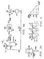
- Fig. 3 illustrates a limited in-rush current driver architecture invented.
- the new architecture is characterized by providing a simple solution using one charge pump 30 as driver with feedback control on a clk duty cycle, wherein no external capacitor is required, i.e. 1 pin saved, and the area required is minimized.
- a battery voltage Vbat is the main system supply voltage.
- a charge pump 30 with slew rate control is used as driver and has a direct connection to a switch device 31.
- the gate capacitance of the switch 31 represents the output capacitor to store the accumulated charge from the charge pump 30. Depending on a specific application this switch device 31 could also be internal if possible.
- a circuit load, 37 e.g. a processor, receives its supply current via the transistor switch 31.
- the drain of the NMOS transistor switch 31 is connected to the output of a buck converter but generally it can be connected to any supply voltage including batteries.
- a key innovation consists in the in-rush current limitation during turn-on and turn-off phases that is achieved through a pulse width modulation (PWM) of the duty cycle of the clock to the charge pump.
- PWM pulse width modulation
- the main building blocks are as shown in Fig. 3a and Fig. 3b :
- the preferred embodiment of the invention comprises disabling the current limiting system to save power between turn on/off periods.
- the on time of the clock signal depends on the slope of the ramp signal: the higher the current is flowing in the switch (highlighted), the steeper the slope of the ramp and therefore the shorter the on time of the clock.
- the ramp generator has two contributions as shown in Fig. 3a and in detail in Fig . 3b :
- Fig. 3b shows in detail illustrates the fix current source Io 381 and in parallel the current source Isw 382 wherein the current generated depends on an in-rush current sensed via a feedback loop.
- duty cycle ref x clk_osc x Cramp / Io + I_inrush x Gi
- Fig. 5 shows simulation results of the present invention.
- Line 50 is a time curve illustrating the output voltage Vpump without applying a slew rate control.
- Line 51 is a time curve illustrating the output voltage Vpump applying the slew rate control of the present invention.
- Line 52 is a time curve illustrating the supply current without applying a slew rate control.
- the maximum in-rush current in this case is 1.30 A.
- Line 53 is a time curve illustrating the supply current applying the slew rate control of the present invention.
- the maximum in-rush current in this case is 0.48 A. A reduction of 63% of the maximum in-rush current has been achieved by the slew-rate control of the present invention.
- Line 54 is a time curve illustrating the clock pulses driving the charge pump without applying the slew rate control.
- Line 55 is a time curve illustrating the clock pulses driving the charge pump applying the slew rate control of the present invention.
- a comparison of both curves 54 and 55 shows clearly that the frequency of both pulses 54 and 55 is equal (fix frequency) but the pulse width of curve 55 is smaller than the pulse width of curve 54 during the turning of the load circuit. Therefore the maximum in-rush current is reduced as shown by the curves 52 and 53 .
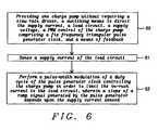
- Fig. 6 illustrates a flowchart of a method invented to limit the in-rush current of a load circuit.
- Step 60 of the method of Fig. 6 illustrates the provision one charge pump without requiring a slew rate driver, a switching means to direct a supply current a load circuit, a supply voltage, a PWM control of the charge pump comprising a fix frequency triangular pulse generator clock, and a means of feedback.
- Step 61 depicts sensing the supply current of the load circuit.
- the last step 62 illustrates performing pulse-width modulation of a duty cycle of the pulse generator clock controlling the charge pump in order to limit the in-rush current to the load circuit, wherein a slope of a ramp signal generated by the pulse generator depends upon the supply current sensed.
Landscapes
- Engineering & Computer Science (AREA)
- Power Engineering (AREA)
- Dc-Dc Converters (AREA)
Abstract
Description
- This invention relates generally to electronic charge pump driving and is specifically applied to a slew rate driver to avoid excessive in-rush current between a dc-dc converter and a load circuit during a turn-on process.
- During the development of power management solutions for mobile electronic devices, particular attention is required to reduce the battery consumption due to leakage of load circuits such as e.g. the CPUs. A common solution is the use of switches between a dc-dc converter and the load circuit (e.g. a processor). These switches isolate electrically the dc-dc converter from the load circuit and require:
- a slew rate controlled driver to avoid excessive in-rush current between the dc-dc converter and the load circuit during the turn-on process.
- a converter, such as a charge pump, able to supply the driver to a voltage above the battery level.
-
Fig. 1 prior art shows a power gating system architecture for such a solution comprising a DC-to-DC converter 1, a charge pump and a slew rate (SR) controlleddriver 2, atransistor switch 3, an arrangement of capacitors C1-C3, and a load circuit (CPU) 4. Although this solution is very effective and allows multiple drivers to share the same charge pump, the continuous need of reducing the turn-on time of the switches requires a dramatic increase in the current delivered by the charge pump. A possible solution would be to increase either the size of the charge pump itself or the size of the external capacitor C3. -
Fig. 2 prior art illustrates an alternative solution to limit the loading on the charge pump comprising of two drivers drv1 and drv2: drv1 supplied from the battery voltage Vbat and drv2 supplied from thecharge pump 20 voltage Vpump. Drv1 is used to charge theswitch gate 21 up to Vbat while drv2 is used only to raise the gate voltage from Vbat to Vpump. The in-rush current is controlled viacapacitive feedback 22 with an internal capacitor to each driver. In summary solution shown inFig. 2 prior art comprises onecharge pump 20, two drivers drv1 and drv2, and oneswitch 21. - This approach requires further circuitry and complications to control the transition between voltage domains and to avoid glitches on the gate during the transition.
- Furthermore when driver drv2 is active, the voltage drop occurring at the output of
charge pump 20 translates into an increase of the resistance of the switch and so to a temporary increase of the power losses. - Although the solution is considered attractive in applications where is required to control multiple switches, it is very inefficient in terms of silicon area (two feedback capacitors and two drivers for each switch) therefore appears to be largely over dimensioned (in both on-chip and off-chip utilization) compared to solutions wherein only one switch is used.
- It is a challenge for engineers to provide a method and circuit to avoid excessive in-rush current that do not have the disadvantages of the existing solutions.
- There are known patents or patent publications dealing with limiting in-rush currents.
- U. S. Patent Application (
US 2010/0013548 to Barrow ) discloses a charge pump, which uses a current limit resistor to limit in-rush current and peak currents. An additional advantage of such a charge pump is that, when being coupled to a boost converter or other switching converter utilizing an inductive energy storage element, it may avoid unnecessary power dissipation caused by the current limit resistor. - U. S. Patent (
US 7,880,530 to Ishiyama ) discloses a power supply circuit which boosts a given voltage to generate one or more power supply voltages including a charge-pump control circuit including switching elements for generating a boost voltage by a charge-pump operation using charge stored in a flying capacitor, a soft-start circuit which prevents a rush current toward the flying capacitor, and a power supply generation circuit which is connected with a stabilization capacitor and generates a power supply voltage using the boost voltage as a power supply. After the power supply generation circuit has been turned ON in a state in which the charge-pump control circuit generates the boost voltage by the charge-pump operation, the switching elements are turned OFF, and the soft-start circuit generates the boost voltage by a charge-pump operation. - U. S. Patent Application Publication (
US 2006/0193156 to Kaishita et al. ) proposes a charge pump DC/DC converter circuit including: a monitor circuit that detects a potential difference between terminals of a semiconductor switch that turns on during a first period, so as to output a determining signal corresponding to the potential difference; and each of drive circuits that outputs a drive signal to a semiconductor switch that turns on during a first period, in response to the determining signal. The drive signal increases the on-resistance of the semiconductor switch in proportion to the detected potential difference. - U. S. Patent Application Publication (
US 2009/0309633 to Kotowski et al. ) proposes a ramp-up circuit for switched capacitor circuits with negative feedback to control the slew rate of in-rush current and other embodiments. - U. S. Patent (
US 6,738,272 to Yamanaka et al .) discloses a charge pump circuit, wherein a constant current circuit is disposed between an input power supply and an output capacitor. When a power supply is started to turn on, the operation of the charge pump circuit is stopped, and the output capacitor is charged up to a given voltage by the constant current circuit, and thereafter the normal operation of the charge pump is started to limit the rush current. When the power supply is started, the operation is conducted by an oscillator circuit having a small duty ratio, and thereafter the control is replaced by the PFM control having the normal duty ratio, to thereby reduce the rush current as compared with that of the conventional PFM control. When the power supply is started, a pre-driver including a current limiting element is used to drive a driver, resulting in such an advantage that the rush current is reduced as compared with that driven by the conventional pre-driver. - U. S. Patent (
US 6,744,224 to Ishii ) teaches an input voltage detecting circuit for detecting an input voltage provided inside a PFM control charge pump circuit, and potential differences between potentials appearing at gate terminals and potentials appearing at source terminals are reduced by gate voltage controlling circuits for in response to a signal from the input voltage detecting circuit, suppressing gate voltages of switch transistors of a charge pump to suppress a rush current value to thereby reduce a current to prevent generation of a noise. - A principal object of the present invention is to use a charge pump as driver for switches with pulse modulation width (PWM) control on the duty cycle of the clock
- A further object of the invention is to reduce the number of external capacitors.
- A further object of the invention is to reduce the on-chip area by embedding the slew rate driving capability inside the charge pump.
- A further object of the present invention is to use a clock generator consisting on a ramp signal with variable slope and a reference voltage, wherein the slope of the ramp signal is dependent on the in-rush current of the switch.
- Moreover an object of the invention is to achieve a simple solution with only one charge pump without requiring a dedicated slew rate control driver.
- In accordance with the objects of this invention a method to limit the in-rush current of a load circuit has been achieved- The method comprises the following steps: (1) providing one charge pump only without requiring a dedicated slew rate driver, a switching means to direct a supply current a load circuit, a supply voltage, a PWM control of the charge pump comprising a fix frequency triangular pulse generator clock, and a means of feedback, (2) sensing a supply current of the load circuit, and (3) performing pulse-width modulation of a duty cycle of the pulse generator performing pulse-width modulation of a duty cycle of the pulse generator clock controlling the charge pump in order to limit the in-rush current to the load circuit, wherein a slope of a ramp signal generated by the pulse generator depends upon the supply current sensed.
- In accordance with the objects of this invention a circuit for a slew rate PWM controlled charge pump for limited in-rush current switch driving has been achieved. The circuit invented comprises, firstly, a port for a main system supply voltage, a fix current source having a first terminal connected to the system supply voltage and a second terminal is connected to a PWM control block, and said variable current source, wherein the current generated depends on the in-rush current sensed via a feedback loop and wherein its second terminal is connected to the PWM control block. Furthermore the circuit comprises: said PWM control block controlling a duty cycle of a clock of a charge pump, said feedback loop, wherein its first terminal is receiving the in-rush current through a load circuit and its second terminal is controlling said variable current source, and said charge pump wherein its output is controlling a switching means. Finally the circuit comprises said switching means wherein a first terminal is connected to the system supply voltage and a second terminal supplies a current through a load circuit, and said load circuit.
- In the accompanying drawings forming a material part of this description, there is shown:
-
Fig. 1 prior art illustrates a solution using switches between a dc-dc converter and a CPU -
Fig. 2 prior art illustrates an alternative solution to limit the loading on the charge pump comprising of two drivers. -
Fig. 3a illustrates a limited in-rush current driver architecture invented. - Fig. 3b shows in detail a fix current source and in parallel a current source wherein the current generated depends on an in-rush current sensed via a feedback loop.
-
Fig. 4 depicts the principles of operation of the PWM control of the present invention. -
Fig. 5 shows simulations results on a model of the proposed invention. -
Fig. 6 illustrates a flowchart of a method invented to limit the in-rush current of a load circuit. - Preferred embodiments of the invention disclose methods and circuits to limit in-rush currents of load circuits.
-
Fig. 3 illustrates a limited in-rush current driver architecture invented. The new architecture is characterized by providing a simple solution using onecharge pump 30 as driver with feedback control on a clk duty cycle, wherein no external capacitor is required, i.e. 1 pin saved, and the area required is minimized. In this preferred embodiment a battery voltage Vbat is the main system supply voltage. - In the new proposed approach a
charge pump 30 with slew rate control is used as driver and has a direct connection to aswitch device 31. - The gate capacitance of the switch 31 (external in the preferred embodiment presented) represents the output capacitor to store the accumulated charge from the
charge pump 30. Depending on a specific application thisswitch device 31 could also be internal if possible. A circuit load, 37, e.g. a processor, receives its supply current via thetransistor switch 31. In the preferred embodiment the drain of theNMOS transistor switch 31 is connected to the output of a buck converter but generally it can be connected to any supply voltage including batteries. - A key innovation consists in the in-rush current limitation during turn-on and turn-off phases that is achieved through a pulse width modulation (PWM) of the duty cycle of the clock to the charge pump.
- The principle of the instant invention works during both in turn on and off transients. When the charge pump has reached its maximum and the switch is fully on, the system (CPU) is completely connected to the supply (buck converter) and no current spikes should occur.
- The main building blocks are as shown in
Fig. 3a and Fig. 3b: - a
charge pump 30 used as driver connected to single supply domain; - one external (or internal)
switch device 31; - a
single capacitive feedback 32 between the switch device and a pulse-width modulation (PWM)control 33; - a fixed 381 and a variable
current source 382 in parallel - the
PWM control 33 comprising:- a fix frequency voltage triangular pulse generator with variable slope proportional to the in-rush current measurement, wherein the pulse generator comprises a clk oscillator (not shown) and a capacitor Cramp; a switch 36 to reset a voltage a reference voltage 34 equivalent to the target value for the in-rush current;
- a short delay
hysteretic comparator 35.
- It should be noted that the principle of the instant invention would work with any kind of feedback. The capacitive feedback described in here is specific for the preferred embodiment of the invention and easy to implement despite the need of an extra external component. It works only in transients and it does not take any DC current between turn on/off periods.
- Once the external switch is completely turned on, no further risks of in-rush currents are expected; therefore the preferred embodiment of the invention comprises disabling the current limiting system to save power between turn on/off periods.
- The principles of operation of the
PWM control 33 are illustrated inFig. 4 . - The on time of the clock signal depends on the slope of the ramp signal: the higher the current is flowing in the switch (highlighted), the steeper the slope of the ramp and therefore the shorter the on time of the clock.
- Consequently the shorter the pulse, the smaller is the charge transferred to the gate of the switch device, which results finally in a limitation of the current in the switch.
- The ramp generator has two contributions as shown in
Fig. 3a and in detail in Fig. 3b: - Io: a fix current source which defines the default slope of the ramp for 50% duty cycle condition when no current is sensed in the switch;
- Isw: a current source proportional to the in-rush current with programmable gain to superimpose the compensation ramp and perform the in-rush current limitation. The higher the current gain (Gi), the steeper the ramp for a certain sense current and the tighter the slew rate limitation.
- Fig. 3b shows in detail illustrates the fix
current source Io 381 and in parallel thecurrent source Isw 382 wherein the current generated depends on an in-rush current sensed via a feedback loop. - The control on the duty cycle can be approximated as:

- ref: is the reference voltage for the PWM comparator;
- clk_osc: is the fix frequency clock;
- Cramp: is the capacitor generating the correction ramp;
- I_inrush: is proportional to the in-rush current.
- Further advantages of this solution are:
- a single driver solution with linear charging of the gate from 0 to Vpump without complicated transitions between supply domains and related voltage drops;
- PWM control and total ramp-up time are independent from battery levels;
- Higher efficiency due to less dissipation paths represented by the absence of drivers in series to the charge pump;
- The charge pump needs to be enabled only when the switch needs to be activated.
- It should be noted that the architecture of a preferred embodiment described above assumes that only one switch is connected at a given time, if more than one switch is connected, the solution is still valid providing that the switches are enabled at the same time.
-
Fig. 5 shows simulation results of the present invention. -
Line 50 is a time curve illustrating the output voltage Vpump without applying a slew rate control.Line 51 is a time curve illustrating the output voltage Vpump applying the slew rate control of the present invention. -
Line 52 is a time curve illustrating the supply current without applying a slew rate control. The maximum in-rush current in this case is 1.30A. Line 53 is a time curve illustrating the supply current applying the slew rate control of the present invention. The maximum in-rush current in this case is 0.48 A. A reduction of 63% of the maximum in-rush current has been achieved by the slew-rate control of the present invention. -
Line 54 is a time curve illustrating the clock pulses driving the charge pump without applying the slew rate control.Line 55 is a time curve illustrating the clock pulses driving the charge pump applying the slew rate control of the present invention. A comparison of bothcurves pulses curve 55 is smaller than the pulse width ofcurve 54 during the turning of the load circuit. Therefore the maximum in-rush current is reduced as shown by thecurves -
Fig. 6 illustrates a flowchart of a method invented to limit the in-rush current of a load circuit. -
Step 60 of the method ofFig. 6 illustrates the provision one charge pump without requiring a slew rate driver, a switching means to direct a supply current a load circuit, a supply voltage, a PWM control of the charge pump comprising a fix frequency triangular pulse generator clock, and a means of feedback.Step 61 depicts sensing the supply current of the load circuit. Thelast step 62 illustrates performing pulse-width modulation of a duty cycle of the pulse generator clock controlling the charge pump in order to limit the in-rush current to the load circuit, wherein a slope of a ramp signal generated by the pulse generator depends upon the supply current sensed. - While the invention has been particularly shown and described with reference to the preferred embodiments thereof, it will be understood by those skilled in the art that various changes in form and details may be made without departing from the spirit and scope of the invention.
Claims (20)
- A method to limit the in-rush current of a load circuit, comprising the following steps:(1) providing one charge pump only without requiring a dedicated slew rate driver, a switching means to direct a supply current a load circuit, a supply voltage, a PWM control of the charge pump comprising a fix frequency triangular pulse generator clock, and a means of feedback;(2) sensing a supply current of the load circuit; and(3) performing pulse-width modulation of a duty cycle of the pulse generator performing pulse-width modulation of a duty cycle of the pulse generator clock controlling the charge pump in order to limit the in-rush current to the load circuit, wherein a slope of a ramp signal generated by the pulse generator depends upon the supply current sensed.
- The method of claim 1 wherein said load circuit can be any load circuit, such as a processor.
- The method of claim 1 wherein said switching means is a transistor switch, and wherein a gate capacitance of said transistor switch is used to store the accumulated charge from the charge pump.
- The method of claim 3 wherein said transistor switch is deployed external of an IC in which the charge pump, the PWM control, and a means of feedback are integrated
- The method of claim 3 wherein said transistor switch is also integrated in the IC and/or .
- The method of claim 1 wherein no external capacitor is required and/or said means of feedback is a capacitive feedback; e.g. a a single capacitive feedback.
- The method of claim 1 wherein said pulse generator generates fix frequency voltage triangular pulses with variable slope.
- The method of claim 1 wherein said PWM control uses a reference voltage equivalent to a target value for the in-rush current, said reference voltage being for instance a first input of a short delay hysteretic comparator.
- The method of claim 1 wherein a ramp voltage of said pulse generator is a second input of hysteretic comparator.
- The method of claim 1 wherein said pulse generator has a fix current contribution, which defines a default slope of the ramp for 50% duty cycle condition when no current is sensed in the switch.
- The method of claim 1 wherein said pulse generator has a current source proportional to the in-rush current with programmable gain to superimpose a compensation ramp and perform the in-rush current limitation.
- The method of claim 1 wherein the current limiting is disabled between turn on/tum/off periods.
- A circuit for a slew rate PWM controlled charge pump for limited in-rush current switch driving, comprising:a port for a main system supply voltage;a fix current source having a first terminal connected to the system supply voltage and a second terminal is connected to a PWM control block;said variable current source, wherein the current generated depends on the in-rush current sensed via a feedback loop and wherein its second terminal is connected to the PWM control block;said PWM control block controlling a duty cycle of a clock of a charge pump;said feedback loop, wherein its first terminal is receiving the in-rush current through a load circuit and its second terminal is controlling said variable current source;said charge pump wherein its output is controlling a switching means;said switching means wherein a first terminal is connected to a supply voltage and a second terminal supplies a current through a load circuit; andsaid load circuit.
- The circuit of claim 13 wherein said feedback loop is a capacitive feedback loop.
- The circuit of claim 13 wherein said PWM control block comprises:a fix frequency voltage triangular pulse generator with variable slope proportional to the in-rush current measurement, wherein its output is connected to a second input of a comparator;a reference voltage equivalent to a target value for the in-rush current wherein the reference voltage is connected to a first input of the comparator; andsaid comparator wherein its output is providing clocking pulses for the charge pump.
- The circuit of claim 15 wherein said comparator is a short delay hysteretic comparator.
- The circuit of claim 15 wherein said pulse generator comprises:a capacitor, having a second terminal connected to ground and a first terminal connected to the second terminal of the variable and fix current sources, to the second input of the comparator, and to a first terminal of a clocking oscillator; and said clocking oscillator, wherein its second terminal is connected to ground.
- The circuit of claim 13 wherein the charge pump is supplied by the main system supply voltage, or by any supply voltage available in the system.
- The circuit of claim 13 wherein the main system supply voltage is a battery voltage or any supply voltage available in the system.
- The circuit of claim 13 wherein said switching means is a transistor having its gate connected to the output of the charge pump, its drain is connected to the system supply voltage, and its source is connected a first terminal of the load circuit, and/or said load circuit is a processor.
Priority Applications (2)
| Application Number | Priority Date | Filing Date | Title |
|---|---|---|---|
| EP11368022A EP2544371A1 (en) | 2011-07-08 | 2011-07-08 | Slew rate PWM controlled charge pump for limited in-rush current switch driving |
| US13/136,143 US8497719B2 (en) | 2011-07-08 | 2011-07-25 | Slew rate PWM controlled charge pump for limited in-rush current switch driving |
Applications Claiming Priority (1)
| Application Number | Priority Date | Filing Date | Title |
|---|---|---|---|
| EP11368022A EP2544371A1 (en) | 2011-07-08 | 2011-07-08 | Slew rate PWM controlled charge pump for limited in-rush current switch driving |
Publications (1)
| Publication Number | Publication Date |
|---|---|
| EP2544371A1 true EP2544371A1 (en) | 2013-01-09 |
Family
ID=45033901
Family Applications (1)
| Application Number | Title | Priority Date | Filing Date |
|---|---|---|---|
| EP11368022A Withdrawn EP2544371A1 (en) | 2011-07-08 | 2011-07-08 | Slew rate PWM controlled charge pump for limited in-rush current switch driving |
Country Status (2)
| Country | Link |
|---|---|
| US (1) | US8497719B2 (en) |
| EP (1) | EP2544371A1 (en) |
Cited By (1)
| Publication number | Priority date | Publication date | Assignee | Title |
|---|---|---|---|---|
| CN106330193A (en) * | 2015-07-02 | 2017-01-11 | 中芯国际集成电路制造(上海)有限公司 | Duty ratio adjustment circuit and analog-to-digital conversion system |
Families Citing this family (7)
| Publication number | Priority date | Publication date | Assignee | Title |
|---|---|---|---|---|
| KR20120078947A (en) * | 2011-01-03 | 2012-07-11 | 페어차일드코리아반도체 주식회사 | Switch control circuit, converter using the same, and switch controlling method |
| US9935480B2 (en) * | 2014-04-29 | 2018-04-03 | Mitsubishi Electric Corporation | Power switch device and system using same |
| EP2978130B1 (en) * | 2014-07-24 | 2019-09-11 | Renesas Electronics Europe GmbH | Circuit for controlling slew rate of a high-side switching element |
| CN106469979B (en) | 2015-08-14 | 2020-08-04 | 恩智浦美国有限公司 | Low voltage ripple charge pump with shared capacitor oscillator |
| US11881280B2 (en) * | 2020-11-30 | 2024-01-23 | Stmicroelectronics International N.V. | Circuit and method for constant slew rate in high voltage charge pumps |
| TWI751878B (en) * | 2021-01-06 | 2022-01-01 | 瑞鼎科技股份有限公司 | Charge pump circuit |
| CN118573010B (en) * | 2024-08-02 | 2024-10-01 | 无锡中微爱芯电子有限公司 | Charge pump with wide power supply voltage range and low surge current |
Citations (11)
| Publication number | Priority date | Publication date | Assignee | Title |
|---|---|---|---|---|
| US5689394A (en) * | 1995-12-04 | 1997-11-18 | General Electric Company | Gate voltage modulation for transistor fault conditions |
| US6313617B1 (en) * | 1997-10-17 | 2001-11-06 | Continental Teves Ag & Co., Ohg | Circuit arrangement for reducing voltage draw down in battery supply lines |
| US6738272B2 (en) | 2001-04-24 | 2004-05-18 | Seiko Instruments Inc. | Charge pump rush current limiting circuit |
| US6744224B2 (en) | 2002-02-06 | 2004-06-01 | Seiko Instruments Inc. | Rush current limiting circuit for a PFM control charge pump |
| US20050174815A1 (en) * | 2004-02-10 | 2005-08-11 | Tien-Tzu Chen | Soft-start charge pump circuit |
| US20050231177A1 (en) * | 2004-04-14 | 2005-10-20 | Koji Tateno | Power supply device and switching power supply device |
| US20060193156A1 (en) | 2005-02-24 | 2006-08-31 | Kenji Kaishita | Charge pump DC/DC converter circuit |
| US20090072803A1 (en) * | 2007-09-19 | 2009-03-19 | Kee-Chee Tiew | Inrush current control |
| US20090309633A1 (en) | 2008-06-17 | 2009-12-17 | Monolithic Power Systems | Charge pump for switched capacitor circuits with slew-rate control of in-rush current |
| US20100013548A1 (en) | 2008-07-18 | 2010-01-21 | Analog Devices, Inc. | Power efficient charge pump with controlled peak currents |
| US7880530B2 (en) | 2006-08-10 | 2011-02-01 | Seiko Epson Corporation | Power supply circuit, display driver, electro-optical device, and electronic instrument |
Family Cites Families (7)
| Publication number | Priority date | Publication date | Assignee | Title |
|---|---|---|---|---|
| US5481178A (en) * | 1993-03-23 | 1996-01-02 | Linear Technology Corporation | Control circuit and method for maintaining high efficiency over broad current ranges in a switching regulator circuit |
| US5773966A (en) * | 1995-11-06 | 1998-06-30 | General Electric Company | Dual-mode, high-efficiency dc-dc converter useful for portable battery-operated equipment |
| US6107862A (en) * | 1997-02-28 | 2000-08-22 | Seiko Instruments Inc. | Charge pump circuit |
| US6331748B1 (en) * | 1998-12-21 | 2001-12-18 | Dongil Technology Ltd. | Driving circuit of a piezo-ceramic transformer capable of controlling an input voltage and a dimming control method thereof |
| JP4579778B2 (en) * | 2004-08-17 | 2010-11-10 | ルネサスエレクトロニクス株式会社 | Sensor power supply circuit and microphone unit using the same |
| JP5196811B2 (en) * | 2007-03-06 | 2013-05-15 | ローム株式会社 | Motor drive device and electric apparatus using the same |
| US20110127978A1 (en) * | 2009-12-02 | 2011-06-02 | Wei-Ching Lee | Pwm controller with low uvlo voltage |
-
2011
- 2011-07-08 EP EP11368022A patent/EP2544371A1/en not_active Withdrawn
- 2011-07-25 US US13/136,143 patent/US8497719B2/en active Active
Patent Citations (11)
| Publication number | Priority date | Publication date | Assignee | Title |
|---|---|---|---|---|
| US5689394A (en) * | 1995-12-04 | 1997-11-18 | General Electric Company | Gate voltage modulation for transistor fault conditions |
| US6313617B1 (en) * | 1997-10-17 | 2001-11-06 | Continental Teves Ag & Co., Ohg | Circuit arrangement for reducing voltage draw down in battery supply lines |
| US6738272B2 (en) | 2001-04-24 | 2004-05-18 | Seiko Instruments Inc. | Charge pump rush current limiting circuit |
| US6744224B2 (en) | 2002-02-06 | 2004-06-01 | Seiko Instruments Inc. | Rush current limiting circuit for a PFM control charge pump |
| US20050174815A1 (en) * | 2004-02-10 | 2005-08-11 | Tien-Tzu Chen | Soft-start charge pump circuit |
| US20050231177A1 (en) * | 2004-04-14 | 2005-10-20 | Koji Tateno | Power supply device and switching power supply device |
| US20060193156A1 (en) | 2005-02-24 | 2006-08-31 | Kenji Kaishita | Charge pump DC/DC converter circuit |
| US7880530B2 (en) | 2006-08-10 | 2011-02-01 | Seiko Epson Corporation | Power supply circuit, display driver, electro-optical device, and electronic instrument |
| US20090072803A1 (en) * | 2007-09-19 | 2009-03-19 | Kee-Chee Tiew | Inrush current control |
| US20090309633A1 (en) | 2008-06-17 | 2009-12-17 | Monolithic Power Systems | Charge pump for switched capacitor circuits with slew-rate control of in-rush current |
| US20100013548A1 (en) | 2008-07-18 | 2010-01-21 | Analog Devices, Inc. | Power efficient charge pump with controlled peak currents |
Cited By (1)
| Publication number | Priority date | Publication date | Assignee | Title |
|---|---|---|---|---|
| CN106330193A (en) * | 2015-07-02 | 2017-01-11 | 中芯国际集成电路制造(上海)有限公司 | Duty ratio adjustment circuit and analog-to-digital conversion system |
Also Published As
| Publication number | Publication date |
|---|---|
| US20110279155A1 (en) | 2011-11-17 |
| US8497719B2 (en) | 2013-07-30 |
Similar Documents
| Publication | Publication Date | Title |
|---|---|---|
| CN106664020B (en) | Shared Bootstrap Capacitors and Methods for Multiphase Buck Converter Circuits | |
| US8497719B2 (en) | Slew rate PWM controlled charge pump for limited in-rush current switch driving | |
| CN102077449B (en) | voltage converter | |
| US9484758B2 (en) | Hybrid bootstrap capacitor refresh technique for charger/converter | |
| US10090663B2 (en) | Over-current protection circuit and method for voltage regulators | |
| US9991794B2 (en) | Hybrid capacitive-inductive voltage converter | |
| CN107465339B (en) | Method and circuit for soft starting high-power charge pump | |
| US8981737B2 (en) | High efficiency PFM control for buck-boost converter | |
| US8890501B2 (en) | System and method for soft-starting a power converter with a pre-charged output | |
| US8000117B2 (en) | Buck boost function based on a capacitor bootstrap input buck converter | |
| CN100588096C (en) | Step-up DC/DC converter and electronic equipment including the same | |
| JP6382002B2 (en) | DC-DC converter | |
| TWI473409B (en) | Constant on-time switching regulator implementing light load control and control method thereof | |
| US20150002115A1 (en) | Series-capacitor buck converter multiphase controller | |
| US20150229212A1 (en) | Switching regulator and control method thereof | |
| US10199919B2 (en) | Zero dead time control circuit | |
| CN104467369A (en) | System and Method for a Switch Driver | |
| CN106855731B (en) | Dual-mode voltage stabilizer circuit | |
| US11387734B2 (en) | Power converter architecture using lower voltage power devices | |
| TWI838215B (en) | Controller and method in controller for switching regulator | |
| US20170063214A1 (en) | Auxiliary recharge | |
| JP2009247202A (en) | Reverse current reduction technique for dc/dc system | |
| US20110001462A1 (en) | Electronic device and method for dc-dc conversion | |
| JP2010130826A (en) | Step-up type switching power supply unit | |
| US20180287496A1 (en) | Inverting buck-boost power converter |
Legal Events
| Date | Code | Title | Description |
|---|---|---|---|
| PUAI | Public reference made under article 153(3) epc to a published international application that has entered the european phase |
Free format text: ORIGINAL CODE: 0009012 |
|
| AK | Designated contracting states |
Kind code of ref document: A1 Designated state(s): AL AT BE BG CH CY CZ DE DK EE ES FI FR GB GR HR HU IE IS IT LI LT LU LV MC MK MT NL NO PL PT RO RS SE SI SK SM TR |
|
| AX | Request for extension of the european patent |
Extension state: BA ME |
|
| 17P | Request for examination filed |
Effective date: 20130708 |
|
| RBV | Designated contracting states (corrected) |
Designated state(s): AL AT BE BG CH CY CZ DE DK EE ES FI FR GB GR HR HU IE IS IT LI LT LU LV MC MK MT NL NO PL PT RO RS SE SI SK SM TR |
|
| STAA | Information on the status of an ep patent application or granted ep patent |
Free format text: STATUS: THE APPLICATION IS DEEMED TO BE WITHDRAWN |
|
| 18D | Application deemed to be withdrawn |
Effective date: 20170201 |