EP2541568B1 - Electrical distribution system including micro electro-mechanical switch (MEMS) devices - Google Patents
Electrical distribution system including micro electro-mechanical switch (MEMS) devices Download PDFInfo
- Publication number
- EP2541568B1 EP2541568B1 EP12173514.6A EP12173514A EP2541568B1 EP 2541568 B1 EP2541568 B1 EP 2541568B1 EP 12173514 A EP12173514 A EP 12173514A EP 2541568 B1 EP2541568 B1 EP 2541568B1
- Authority
- EP
- European Patent Office
- Prior art keywords
- mems
- circuit
- halt
- circuit breaker
- electrical
- Prior art date
- Legal status (The legal status is an assumption and is not a legal conclusion. Google has not performed a legal analysis and makes no representation as to the accuracy of the status listed.)
- Active
Links
Images

Classifications
-
- H—ELECTRICITY
- H01—ELECTRIC ELEMENTS
- H01H—ELECTRIC SWITCHES; RELAYS; SELECTORS; EMERGENCY PROTECTIVE DEVICES
- H01H9/00—Details of switching devices, not covered by groups H01H1/00 - H01H7/00
- H01H9/54—Circuit arrangements not adapted to a particular application of the switching device and for which no provision exists elsewhere
- H01H9/541—Contacts shunted by semiconductor devices
- H01H9/542—Contacts shunted by static switch means
-
- H—ELECTRICITY
- H01—ELECTRIC ELEMENTS
- H01H—ELECTRIC SWITCHES; RELAYS; SELECTORS; EMERGENCY PROTECTIVE DEVICES
- H01H1/00—Contacts
- H01H1/0036—Switches making use of microelectromechanical systems [MEMS]
-
- H—ELECTRICITY
- H01—ELECTRIC ELEMENTS
- H01H—ELECTRIC SWITCHES; RELAYS; SELECTORS; EMERGENCY PROTECTIVE DEVICES
- H01H9/00—Details of switching devices, not covered by groups H01H1/00 - H01H7/00
- H01H9/54—Circuit arrangements not adapted to a particular application of the switching device and for which no provision exists elsewhere
- H01H9/541—Contacts shunted by semiconductor devices
- H01H9/542—Contacts shunted by static switch means
- H01H2009/543—Contacts shunted by static switch means third parallel branch comprising an energy absorber, e.g. MOV, PTC, Zener
-
- H—ELECTRICITY
- H01—ELECTRIC ELEMENTS
- H01H—ELECTRIC SWITCHES; RELAYS; SELECTORS; EMERGENCY PROTECTIVE DEVICES
- H01H71/00—Details of the protective switches or relays covered by groups H01H73/00 - H01H83/00
- H01H2071/008—Protective switches or relays using micromechanics
-
- H—ELECTRICITY
- H01—ELECTRIC ELEMENTS
- H01H—ELECTRIC SWITCHES; RELAYS; SELECTORS; EMERGENCY PROTECTIVE DEVICES
- H01H83/00—Protective switches, e.g. circuit-breaking switches, or protective relays operated by abnormal electrical conditions otherwise than solely by excess current
- H01H83/20—Protective switches, e.g. circuit-breaking switches, or protective relays operated by abnormal electrical conditions otherwise than solely by excess current operated by excess current as well as by some other abnormal electrical condition
- H01H2083/201—Protective switches, e.g. circuit-breaking switches, or protective relays operated by abnormal electrical conditions otherwise than solely by excess current operated by excess current as well as by some other abnormal electrical condition the other abnormal electrical condition being an arc fault
-
- H—ELECTRICITY
- H01—ELECTRIC ELEMENTS
- H01H—ELECTRIC SWITCHES; RELAYS; SELECTORS; EMERGENCY PROTECTIVE DEVICES
- H01H83/00—Protective switches, e.g. circuit-breaking switches, or protective relays operated by abnormal electrical conditions otherwise than solely by excess current
- H01H83/20—Protective switches, e.g. circuit-breaking switches, or protective relays operated by abnormal electrical conditions otherwise than solely by excess current operated by excess current as well as by some other abnormal electrical condition
- H01H83/22—Protective switches, e.g. circuit-breaking switches, or protective relays operated by abnormal electrical conditions otherwise than solely by excess current operated by excess current as well as by some other abnormal electrical condition the other condition being unbalance of two or more currents or voltages
Definitions
- MEMS micro electro-mechanical switch
- US 2008/0310058 A1 and WO 2008/153575 A1 disclose MEMS based switching systems in which a current/voltage sensor of an over-current protection component continuously monitors either a current level or a voltage level within a system.
- Circuit breakers are used to protect electrical circuits from damage due to an overload condition or a short circuit condition. Certain circuit breakers provide protection to uses by sensing ground and arc fault conditions. Upon sensing an overload, a short circuit condition, and/or a fault, the circuit breaker interrupts power to the electric circuit to prevent, or at least minimize, damage to circuit components and/or prevent injury.
- circuit breakers independently sense and respond to an over current condition in an associated electrical circuit. As such, each circuit breaker must include dedicated current sensing devices, thermal sensing devices, control devices, and mechanical switch devices. The mechanical switch devices are operated by the control devices to cut-off electrical current passing through the circuit breaker in response to signals indicating an over current condition or short circuit from the current and thermal sensing devices.
- the present invention provides an electrical load center as defined in claim 1.
- Load center 2 includes a main housing 6 having a base wall 8, first and second opposing side walls 10 and 11, and third and fourth opposing side walls 13 and 14 that collectively define an interior portion 18.
- Load center 2 is also shown to include first and second bus bars 24 and 25, first and second neutral bars 27 and 28, and first and second control buses 30 and 31 mounted to base wall 8.
- a main circuit breaker 34 controls passage of an electric current from a mains supply (not shown) to first and second bus bars 24 and 25.
- Load center 2 also includes a micro electro-mechanical switch (MEMS) based electric distribution system 40 that controls passage of an electrical current between first and second bus bars 24 and 25 and a plurality of branch circuits (not shown).
- MEMS micro electro-mechanical switch
- Electric distribution system 40 includes a MEMS control board 44 connected to first and second bus bars 24 and 25 as well as first and second control busses 30 and 31.
- MEMS control board 44 selectively controls a plurality of Hybrid Arcless Limiting Technology (HALT) boards 46 and 47 which in turn signal a plurality of MEMS circuit breaker devices 49-54 and 60a-60v.
- MEMS circuit breaker devices 49-54 constitute dual pole circuit breaker elements that are connected to each of first and second bus bars 24 and 25, while MEMS circuit breaker devices 60a-60v constitute single pole circuit breaker elements that are each connected to a single one of first and second bus bars 24 and 25. That is, circuit breaker devices 60a-60k are coupled to first bus bar 24 and circuit breaker boards 601-60v are coupled to second bus bar 25.
- FIG. 2 As each circuit breaker board is substantially similar, a detailed description will follow with reference to FIG. 2 in describing circuit breaker board 60a with an understanding that circuit breaker boards 49-54 and 60b-60v include similar structure.
- circuit breaker board 60a includes a switching system 70 having a MEMS switch array 74 that is closely coupled to a plurality of comer diodes 78-81.
- MEMS switch array 74 is connected at center points (not separately labeled) of a balanced diode bridge (not separately labeled) formed by diode 78-81.
- the term "closely coupled” should be understood to mean that MEMS switch array 74 is coupled to comer diodes 78-81 with as small of a loop area as possible so as to limit the voltage created by stray inductance associated with the loop area to below about 1V.
- the loop area is defined as the area between each MEMS device or die in MEMS switch array 74 and the balanced diode bridge.
- an inductive voltage drop across MEMS switch array 74 during a switching event is controlled by maintaining a small loop inductance between MEMS switch array 74 and comer diodes 78-81.
- the inductive voltage across MEMS switch array 74 during switching is determined by three factors: The length of the loop area which establishes the level of stray inductance; MEMS switch current that is between about 1 A and about 10 A per parallel leg; and MEMS switching time which is about 1 ⁇ sec.
- each die in MEMS switch array 74 carries about 10 A of current and can switch in approximately 1 microsecond.
- total current transferred to the diode bridge would be 2 times the die capability or 20 A.
- V L*di/dt
- stray inductance would be held to no more than about 50 nH.
- stray inductance could be as high as about 500nH.
- the desired loop area can be achieved by, for example, mounting MEMS switch array 74 on one side of a circuit board (not separately labeled) and comer diodes 78-81 on another side of the circuit board, directly opposite MEMS switch array 74.
- comer diodes 78-81 could be positioned directly between two parallel arrangements of MEMS dies as will be discussed more fully below.
- comer diodes 78-81 could be integrally formed within one ore more of the MEMS dies.
- MEMS switch array 74 and comer diodes 78-81 can vary so long as the loop area, and, by extension, inductance, is maintained as small as possible. While embodiments of the invention are described employing corner diodes 78-81, it will be appreciated that the term "corner” is not limited to a physical location of the diodes, but is more directed to a placement of the diodes relative to the MEMS dies.
- corner diodes 78-81 are arranged in a balanced diode bridge so as to provide a low impedance path for load current passing through MEMS switch array 74.
- corner diodes 78-81 are arranged so as to limit inductance which, in turn, limits voltage changes over time, i.e., voltage spikes across MEMS switch array 74.
- the balanced diode bridge includes a first branch 85 and a second branch 86.
- the term "balanced diode bridge" describes a diode bridge that is configured such that voltage drops across both the first and second branches 85 and 86 are substantially equal when current in each branch 85, 86 is substantially equal.
- first branch 85 diode 78 and diode 79 are coupled together to form a first series circuit (not separately labeled).
- second branch 86 includes diode 80 and diode 81 operatively coupled together to form a second series circuit (also not separately labeled).
- the balanced diode bridge is also shown to include connection points 89 and 90 that connect with one of first and second bus bars 24 and 25.
- MEMS switch array 74 includes a first MEMS switch leg 95 connected in series (m) and a second MEMS switch leg 96 also connected in series (m). More specifically, first MEMS switch leg 95 includes a first MEMS die 104, a second MEMS die 105, a third MEMS die 106, and a fourth MEMS die 107 connected in series. Likewise, second MEMS switch leg 96 includes a fifth MEMS die 110, a sixth MEMS die 111, a seventh MEMS die 112 and an eighth MEMS die 113 that are connected in series. At this point it should be understood that each MEMS die 104-107 and 110-113 can be configured to include multiple MEMS switches.
- each MEMS die 104-107 and 110-113 includes 50 - 100 MEMS switches.
- the number of switches for each die 104-107 and 110-113 could vary.
- First MEMS switch leg 95 is connected in parallel (n) to second MEMS switch leg 96.
- first and second MEMS switch legs 95, 96 form an (m X n) array which, in the example embodiment shown, is a (4 X 2) array.
- m X n is a (4 X 2) array.
- MEMS switch 104 includes a first connection 116, a second connection 117, and a third connection 118.
- first connection 116 may be configured as a drain connection
- second connection 117 may be configured as a source connection
- third connection 118 may be configured as a gate connection.
- Gate connection 118 is connected to MEMS switch 110 and to a first gate driver 125.
- First gate driver 125 is associated with MEMS switches 104, 105, 110, and 111.
- a second gate driver 126 is associated with MEMS switches 106, 107, 112, and 113.
- Each gate driver 125, 126 includes multiple isolated outputs (not separately labeled) that are electrically coupled to MEMS switches 104-107 and 110-113 as shown.
- First and second gate drivers 125 and 126 also include corresponding control connections 129 and 130 that are connected to MEMS control board 44 through control bus 30. With this arrangement, gate drivers 125 and 126 provide the means for selectively changing the state (open/closed) of MEMS switches 104-107, and 110-113.
- switching system 70 includes a plurality of grading networks connected to first and second MEMS switch legs 95 and 96. More specifically, switching system 70 includes a first grading network 134 electrically connected, in parallel, to first and fifth MEMS switches 104 and 110, a second grading network 135 is electrically connected, in parallel, to second and sixth MEMS switches 105 and 111, a third grading network 136 is electrically connected, in parallel, to third and seventh MEMS switches 106 and 112, and a fourth grading network 137 is electrically connected, in parallel, to fourth and eighth MEMS switches 107 and 113.
- First grading network 134 includes a first resistor 140 connected in parallel to a first capacitor 141.
- First resistor 140 has a value of about 10K ohms and first capacitor 141 has a value of about 0.1 ⁇ F.
- Second grading network 135 includes a second resistor 143 connected in parallel with a second capacitor 144. Second resistor 143 and second capacitor 144 are similar to first resistor 140 and first capacitor 141 respectively.
- Third grading network 136 includes a third resistor 146 and a third capacitor 147. Third resistor 146 and third capacitor 147 are similar to first resistor 140 and first capacitor 141 respectively.
- fourth grading network 137 includes a fourth resistor 149 and a fourth capacitor 150.
- Fourth resistor 149 and fourth capacitor 150 are similar to first resistor 140 and first capacitor 141 respectively.
- Grading networks 134-137 aid in changing position of corresponding ones of MEMS switches 104-107 and 110-113. More specifically, grading networks 134-137 ensure a uniform voltage distribution across each MEMS element connected in series.
- Switching system 70 is also shown to include a first intermediate branch circuit 154, a second intermediate branch circuit 155, a third intermediate branch circuit 156, a fourth intermediate branch circuit 157, a fifth intermediate branch circuit 158 and a sixth intermediate branch circuit 159.
- Intermediate branch circuits 154-159 are electrically connected between respective ones of first and second gate drivers 125 and 126 and first and second branches 85 and 86 of the balanced diode bridge. More specifically, first, second and fifth intermediate branch circuits 154, 155 and 158 are connected between first branch 85 and first grading network 134; and third, fourth, and sixth intermediate branch circuits 156, 157, and 159 are connected between second branch 86 and third grading network 136.
- fifth and sixth intermediate branch circuits 158 and 159 are coupled between a HALT connection point having a first HALT connector member 160 and a second HALT connector 161.
- First intermediate branch circuit 154 includes a first intermediate diode 163 and a first intermediate resistor 164.
- the term intermediate diode should be understood to mean a diode that is connected across only a portion of MEMS switch array 74 as opposed to a corner diode that is connected across the entirety of MEMS switch array 74.
- Second intermediate branch circuit 155 includes a second intermediate diode 166 and a second intermediate resistor 167.
- Third intermediate branch circuit 156 includes a third intermediate diode 169 and a third intermediate resistor 170, and fourth intermediate branch circuit 157 includes a fourth intermediate diode 172 and a fourth intermediate resistor 173.
- Fifth intermediate branch circuit 158 includes a fifth intermediate diode 175 and a fifth intermediate resistor 176.
- sixth intermediate branch circuit 158 includes a sixth intermediate diode 178 and a sixth intermediate resistor 179.
- the arrangement of intermediate diodes 163, 166, 169, 172, 175, and 178 and intermediate resistors 164, 167, 170, 173, 176, and 179 ensures that current flow through intermediate branch circuits 154-159 remains low thereby allowing for a the use of lower rated circuit components. In this manner the cost and size of the intermediate diodes remains low.
- a higher current rating i.e., a current rating in the range of worst possible current flowing through load under a fault condition. While all other diodes of MEMS array can be of much smaller current rating.
- Switching system 70 is further shown to include a voltage snubber 181 that is connected in parallel with first and second pluralities of MEMS switches 104-107 and 110-113. Voltage snubber 181 limits voltage overshoot during fast contact separation of each of MEMS switches 104-107 and 110-113. Voltage snubber 181 is shown in the form of a metal-oxide varistor (MOV) 182. However, it should be appreciated by one of ordinary skill in the art that voltage snubber 181 can take on a variety of forms including circuits having a snubber capacitor connected in series with a snubber resistor. Switching system 70 is also shown to include a HALT switch connection 184 that connects fifth intermediate branch circuit 158 to an associated one of HALT boards 46 and 47 to power a HALT circuit 190 arranged on HALT board 46 as will be described more fully below.
- HALT switch connection 184 that connects fifth intermediate branch circuit 158 to an associated one of HALT boards 46 and 47 to power
- HALT board 46 includes a HALT circuit 190 that facilitates the introduction of a protective pulse to switching system 70.
- HALT circuit 190 includes a HALT capacitor 192 coupled in series with a HALT inductor coil 193.
- HALT circuit 190 is further shown to include a HALT activation switch 196 as well as a pair of terminals or connectors 199 and 200.
- Connectors 199 and 200 provide an interface with switching system 70. More specifically, connectors 199 and 200 are electrically connected between first and second HALT connector members 160 and 161.
- HALT activation switch 196 is selectively closed to electrically connect HALT circuit 190 to switching system 70 to trigger MEMS switches 104-107 and 111-113 to pass an electrical current between connection points 89 and 90.
- HALT circuit 190 is also selectively activated to trigger MEMS switches 104-107 and 111-113 to open thereby cutting off current flow between connection points 89 and 90.
- switching system 70 may be electrically connected to multiple HALT circuits. For example, it may be desirable to employ a primary HALT circuit and a secondary HALT circuit.
- the primary HALT circuit is employed to, for example, close the circuit breaker device allowing current flow
- the secondary HALT circuit is employed to immediately open the circuit breaker device and cut off current flow in the event that a fault is detected. That is, the secondary HALT device provides a back up to the primary HALT circuit allowing for multiple circuit breaker device responses without the need to wait for HALT components to re-energize.
- MEMS control board 44 includes a central processor (CPU) 204 that is may include a ground fault circuit interruption (GFCI) module and logic 207, and an arc fault circuit interruption module and logic 209. MEMS control board 44 is also shown to include first and second power terminals 218 and 219 that are coupled to first and second bus bars 24 and 25 as well as first and second control terminals 222 and 223 that are coupled to control busses 30 and 31. With this arrangement, MEMS control board 44 monitors electrical current flow data from each circuit breaker board 49-54 and 60a-60v.
- CPU central processor
- GFCI ground fault circuit interruption
- MEMS control board 44 In the event of user selected opening/closing or a fault condition, such as a ground fault, arc fault or a short circuit, MEMS control board 44 will open the switching system associated with the circuit breaker board 49-54 and 60a-60v experiencing the fault to protect the branch circuits. MEMS control board 44 receives current flow data from a current sensor such as shown at 240 in FIG. 2 , mounted to each circuit breaker board 49-54 and 60a-60v.
- FIG. 5 in describing a method 280 of opening/closing switching system 70.
- a decision is reached in CPU 204 to change a position of switching system 70 as indicated in block 300.
- CPU 204 checks the readiness of HALT circuit 190 in block 302. If HALT circuit 190 is ready, primary HALT switch 196 is closed as indicated in block 304. If HALT circuit 190 is not ready, secondary HALT switch 197 is closed as indicated in block 306. By ready it should be understood that if voltage is not above a predetermined threshold, the HALT circuit will not posses enough energy to activate the circuit breaker device and provide protection.
- HALT circuit may be employed, or there may be a pause to allow the HALT circuit time to re-energize.
- the HALT switch on the associated MEMS circuit board is closed as indicated in block 308.
- HALT current flows to the diode bridge on the MEMS circuit board as indicate in block 310.
- a determination is made whether to open or close the switching system in block 320. If closing the switching system, CPU 204 passes a signal through one of the first and second control busses 30 and 31 to the gate drivers on the associated MEMS circuit breaker device causing the MEMS switches to change position and pass electrical current as indicated in block 322.
- CPU 204 cuts off the signal through one of the first and second control busses 30 and 31 to the gate drivers on the associated MEMS circuit breaker device causing the MEMS switches to change position and open thereby interrupting current flow through the associated MEMS circuit breaker device as indicated in block 324.
- FIG. 6 in describing a method 380 of deciding to open a switch assembly in accordance with an example embodiment.
- Current passing through the switch assembly is monitored as indicated in block 400.
- Current sensing module 211 monitors for a short circuit and GFCI module monitors for a ground fault as indicated in block 402. If no short circuit or ground fault is found, voltage is monitored as indicated in block 404 and AFCI module 209 monitors for arc faults in block 406.
- CPU 204 also monitors for user input in block 408.
- method 280 is initiated to open the switch assembly as indicated in block 420 to protect the branch circuit associated with the affected MEMS circuit breaker.
- the present invention provides a system that utilizes MEMS devices to pass and/or interrupt current between electrical mains and branch circuits.
- the MEMS devices are controlled by a MEMS control board that monitors current and voltage. In the event of a current or voltage fault, the MEMS control board signals the MEMS device(s) to open and interrupt current flow.
- the use of a MEMS control board removes the need to provide dedicated ground fault, arc fault and short circuit monitoring at each circuit breaker.
- the use of MEMS devices will lead to a size and cost reduction for each circuit breaker. It should be also understood that current and voltage ratings for each MEMS device can vary based on a particular circuit rating.
- MEMS devices/dies used in a particular MEMS circuit breaker can also vary.
- example embodiments can be incorporated into a wide array of electrical protection devices or systems that would benefit from circuit monitoring and protection.
Description
- The subject matter disclosed herein relates to the art of electrical control systems and, more particularly, to an electrical distribution system including micro electro-mechanical switch (MEMS) devices.
-
US 2008/0310058 A1 andWO 2008/153575 A1 disclose MEMS based switching systems in which a current/voltage sensor of an over-current protection component continuously monitors either a current level or a voltage level within a system. - Circuit breakers are used to protect electrical circuits from damage due to an overload condition or a short circuit condition. Certain circuit breakers provide protection to uses by sensing ground and arc fault conditions. Upon sensing an overload, a short circuit condition, and/or a fault, the circuit breaker interrupts power to the electric circuit to prevent, or at least minimize, damage to circuit components and/or prevent injury. Currently, circuit breakers independently sense and respond to an over current condition in an associated electrical circuit. As such, each circuit breaker must include dedicated current sensing devices, thermal sensing devices, control devices, and mechanical switch devices. The mechanical switch devices are operated by the control devices to cut-off electrical current passing through the circuit breaker in response to signals indicating an over current condition or short circuit from the current and thermal sensing devices.
- The present invention provides an electrical load center as defined in claim 1.
- These and other advantages and features will become more apparent from the following description taken in conjunction with the drawings.
- The subject matter, which is regarded as the invention, is particularly pointed out and distinctly claimed in the claims at the conclusion of the specification. The foregoing and other features, and advantages of the invention are apparent from the following detailed description taken in conjunction with the accompanying drawings in which:
-
FIG. 1 is a partial perspective view of an electrical distribution system including a plurality of micro electro-mechanical switch (MEMS) devices in accordance with an example embodiment; -
FIG. 2 is a schematic drawing illustrating a MEMS circuit breaker device in accordance with an example embodiment; -
FIG. 3 is a schematic view of a Hybrid Arcless Limiting Technology (HALT) circuit board in accordance with an example embodiment; -
FIG. 4 is a block diagram illustrating a MEMS control board in accordance with one aspect of the example embodiment; -
FIG. 5 is a flow diagram illustrating a method of changing a state of the MEMS circuit breaker device ofFIG. 2 ; and -
FIG. 6 is a flow diagram illustrating a method of opening the MEMS circuit breaker device ofFIG. 2 . - The detailed description explains embodiments of the invention, together with advantages and features, by way of example with reference to the drawings.
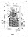
- With reference to
FIG. 1 , a load center in accordance with an example embodiment is indicated generally at 2.Load center 2 includes amain housing 6 having abase wall 8, first and secondopposing side walls opposing side walls interior portion 18.Load center 2 is also shown to include first andsecond bus bars neutral bars second control buses base wall 8. Amain circuit breaker 34 controls passage of an electric current from a mains supply (not shown) to first andsecond bus bars Load center 2 also includes a micro electro-mechanical switch (MEMS) basedelectric distribution system 40 that controls passage of an electrical current between first andsecond bus bars -
Electric distribution system 40 includes aMEMS control board 44 connected to first andsecond bus bars second control busses control board 44 selectively controls a plurality of Hybrid Arcless Limiting Technology (HALT)boards second bus bars circuit breaker devices 60a-60v constitute single pole circuit breaker elements that are each connected to a single one of first andsecond bus bars circuit breaker devices 60a-60k are coupled tofirst bus bar 24 and circuit breaker boards 601-60v are coupled tosecond bus bar 25. As each circuit breaker board is substantially similar, a detailed description will follow with reference toFIG. 2 in describingcircuit breaker board 60a with an understanding that circuit breaker boards 49-54 and 60b-60v include similar structure. - In accordance with an example embodiment,
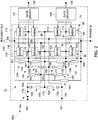
circuit breaker board 60a includes aswitching system 70 having aMEMS switch array 74 that is closely coupled to a plurality of comer diodes 78-81.MEMS switch array 74 is connected at center points (not separately labeled) of a balanced diode bridge (not separately labeled) formed by diode 78-81. The term "closely coupled" should be understood to mean thatMEMS switch array 74 is coupled to comer diodes 78-81 with as small of a loop area as possible so as to limit the voltage created by stray inductance associated with the loop area to below about 1V. The loop area is defined as the area between each MEMS device or die inMEMS switch array 74 and the balanced diode bridge. In accordance with one aspect of the example embodiment, an inductive voltage drop acrossMEMS switch array 74 during a switching event is controlled by maintaining a small loop inductance betweenMEMS switch array 74 and comer diodes 78-81. The inductive voltage acrossMEMS switch array 74 during switching is determined by three factors: The length of the loop area which establishes the level of stray inductance; MEMS switch current that is between about 1 A and about 10 A per parallel leg; and MEMS switching time which is about 1 µsec. - In accordance with one aspect of the example embodiment, each die in
MEMS switch array 74 carries about 10 A of current and can switch in approximately 1 microsecond. In further accordance with the example aspect, total current transferred to the diode bridge would be 2 times the die capability or 20 A. Given the equation V = L*di/dt, stray inductance would be held to no more than about 50 nH. However, if each die in MEMS switch array was configured to carry 1 A, then stray inductance could be as high as about 500nH. - In still further accordance with the example embodiment, the desired loop area can be achieved by, for example, mounting
MEMS switch array 74 on one side of a circuit board (not separately labeled) and comer diodes 78-81 on another side of the circuit board, directly oppositeMEMS switch array 74. In accordance with another example, comer diodes 78-81 could be positioned directly between two parallel arrangements of MEMS dies as will be discussed more fully below. In accordance with still another example, comer diodes 78-81 could be integrally formed within one ore more of the MEMS dies. In any event, it should be understood that the particular arrangement ofMEMS switch array 74 and comer diodes 78-81 can vary so long as the loop area, and, by extension, inductance, is maintained as small as possible. While embodiments of the invention are described employing corner diodes 78-81, it will be appreciated that the term "corner" is not limited to a physical location of the diodes, but is more directed to a placement of the diodes relative to the MEMS dies. - As discussed above, corner diodes 78-81 are arranged in a balanced diode bridge so as to provide a low impedance path for load current passing through
MEMS switch array 74. As such, corner diodes 78-81 are arranged so as to limit inductance which, in turn, limits voltage changes over time, i.e., voltage spikes acrossMEMS switch array 74. In the example embodiment shown, the balanced diode bridge includes afirst branch 85 and asecond branch 86. As used herein, the term "balanced diode bridge" describes a diode bridge that is configured such that voltage drops across both the first andsecond branches branch first branch 85, diode 78 anddiode 79 are coupled together to form a first series circuit (not separately labeled). In a similar fashion,second branch 86 includes diode 80 anddiode 81 operatively coupled together to form a second series circuit (also not separately labeled). The balanced diode bridge is also shown to includeconnection points second bus bars - In further accordance with an example embodiment,
MEMS switch array 74 includes a firstMEMS switch leg 95 connected in series (m) and a secondMEMS switch leg 96 also connected in series (m). More specifically, firstMEMS switch leg 95 includes a first MEMS die 104, a second MEMS die 105, a third MEMS die 106, and a fourth MEMS die 107 connected in series. Likewise, secondMEMS switch leg 96 includes a fifth MEMS die 110, a sixth MEMS die 111, a seventh MEMS die 112 and an eighth MEMS die 113 that are connected in series. At this point it should be understood that each MEMS die 104-107 and 110-113 can be configured to include multiple MEMS switches. In accordance with one aspect of the example embodiment, each MEMS die 104-107 and 110-113 includes 50 - 100 MEMS switches. However, the number of switches for each die 104-107 and 110-113 could vary. FirstMEMS switch leg 95 is connected in parallel (n) to secondMEMS switch leg 96. With this arrangement, first and secondMEMS switch legs - As each MEMS switch 104-107 and 110-113 includes similar connections, a detailed description will follow with reference to
MEMS switch 104 with an understanding that the remaining MEMS switches 105-107 and 110-113 include corresponding connections.MEMS switch 104 includes afirst connection 116, asecond connection 117, and athird connection 118. In one embodiment,first connection 116 may be configured as a drain connection,second connection 117 may be configured as a source connection andthird connection 118 may be configured as a gate connection.Gate connection 118 is connected toMEMS switch 110 and to afirst gate driver 125.First gate driver 125 is associated withMEMS switches second gate driver 126 is associated withMEMS switches gate driver second gate drivers control connections MEMS control board 44 throughcontrol bus 30. With this arrangement,gate drivers - In still further accordance with an example embodiment, switching
system 70 includes a plurality of grading networks connected to first and secondMEMS switch legs system 70 includes afirst grading network 134 electrically connected, in parallel, to first and fifth MEMS switches 104 and 110, asecond grading network 135 is electrically connected, in parallel, to second and sixth MEMS switches 105 and 111, athird grading network 136 is electrically connected, in parallel, to third and seventh MEMS switches 106 and 112, and afourth grading network 137 is electrically connected, in parallel, to fourth and eighth MEMS switches 107 and 113. -
First grading network 134 includes afirst resistor 140 connected in parallel to afirst capacitor 141.First resistor 140 has a value of about 10K ohms andfirst capacitor 141 has a value of about 0.1 µF. Of course it should be understood that the values offirst resistor 140 andfirst capacitor 141 can vary.Second grading network 135 includes asecond resistor 143 connected in parallel with asecond capacitor 144.Second resistor 143 andsecond capacitor 144 are similar tofirst resistor 140 andfirst capacitor 141 respectively.Third grading network 136 includes athird resistor 146 and athird capacitor 147.Third resistor 146 andthird capacitor 147 are similar tofirst resistor 140 andfirst capacitor 141 respectively. Finally,fourth grading network 137 includes afourth resistor 149 and afourth capacitor 150.Fourth resistor 149 andfourth capacitor 150 are similar tofirst resistor 140 andfirst capacitor 141 respectively. Grading networks 134-137 aid in changing position of corresponding ones of MEMS switches 104-107 and 110-113. More specifically, grading networks 134-137 ensure a uniform voltage distribution across each MEMS element connected in series. -
Switching system 70 is also shown to include a firstintermediate branch circuit 154, a secondintermediate branch circuit 155, a thirdintermediate branch circuit 156, a fourthintermediate branch circuit 157, a fifthintermediate branch circuit 158 and a sixthintermediate branch circuit 159. Intermediate branch circuits 154-159 are electrically connected between respective ones of first andsecond gate drivers second branches intermediate branch circuits first branch 85 andfirst grading network 134; and third, fourth, and sixthintermediate branch circuits second branch 86 andthird grading network 136. In addition, fifth and sixthintermediate branch circuits HALT connector member 160 and asecond HALT connector 161. - First
intermediate branch circuit 154 includes a firstintermediate diode 163 and a firstintermediate resistor 164. The term intermediate diode should be understood to mean a diode that is connected across only a portion ofMEMS switch array 74 as opposed to a corner diode that is connected across the entirety ofMEMS switch array 74. Secondintermediate branch circuit 155 includes a secondintermediate diode 166 and a secondintermediate resistor 167. Thirdintermediate branch circuit 156 includes a thirdintermediate diode 169 and a thirdintermediate resistor 170, and fourthintermediate branch circuit 157 includes a fourthintermediate diode 172 and a fourthintermediate resistor 173. Fifthintermediate branch circuit 158 includes a fifthintermediate diode 175 and a fifthintermediate resistor 176. Finally, sixthintermediate branch circuit 158 includes a sixthintermediate diode 178 and a sixthintermediate resistor 179. The arrangement ofintermediate diodes intermediate resistors -
Switching system 70 is further shown to include avoltage snubber 181 that is connected in parallel with first and second pluralities of MEMS switches 104-107 and 110-113.Voltage snubber 181 limits voltage overshoot during fast contact separation of each of MEMS switches 104-107 and 110-113.Voltage snubber 181 is shown in the form of a metal-oxide varistor (MOV) 182. However, it should be appreciated by one of ordinary skill in the art thatvoltage snubber 181 can take on a variety of forms including circuits having a snubber capacitor connected in series with a snubber resistor.Switching system 70 is also shown to include aHALT switch connection 184 that connects fifthintermediate branch circuit 158 to an associated one ofHALT boards HALT circuit 190 arranged onHALT board 46 as will be described more fully below. - Reference will now be made to
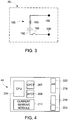
FIG. 3 in describingHALT board 46 with an understanding that HALTboard 47 includes similar components.HALT board 46 includes aHALT circuit 190 that facilitates the introduction of a protective pulse to switchingsystem 70.HALT circuit 190 includes aHALT capacitor 192 coupled in series with aHALT inductor coil 193.HALT circuit 190 is further shown to include aHALT activation switch 196 as well as a pair of terminals orconnectors Connectors system 70. More specifically,connectors HALT connector members HALT activation switch 196 is selectively closed to electrically connectHALT circuit 190 to switchingsystem 70 to trigger MEMS switches 104-107 and 111-113 to pass an electrical current between connection points 89 and 90.HALT circuit 190 is also selectively activated to trigger MEMS switches 104-107 and 111-113 to open thereby cutting off current flow between connection points 89 and 90. In addition, it should be understood, that switchingsystem 70 may be electrically connected to multiple HALT circuits. For example, it may be desirable to employ a primary HALT circuit and a secondary HALT circuit. The primary HALT circuit is employed to, for example, close the circuit breaker device allowing current flow, and the secondary HALT circuit is employed to immediately open the circuit breaker device and cut off current flow in the event that a fault is detected. That is, the secondary HALT device provides a back up to the primary HALT circuit allowing for multiple circuit breaker device responses without the need to wait for HALT components to re-energize. - Reference will now be made to
FIG. 4 in describingMEMS control board 44 in accordance with one aspect of the example embodiment.MEMS control board 44 includes a central processor (CPU) 204 that is may include a ground fault circuit interruption (GFCI) module andlogic 207, and an arc fault circuit interruption module andlogic 209.MEMS control board 44 is also shown to include first andsecond power terminals second control terminals busses MEMS control board 44 monitors electrical current flow data from each circuit breaker board 49-54 and 60a-60v. In the event of user selected opening/closing or a fault condition, such as a ground fault, arc fault or a short circuit,MEMS control board 44 will open the switching system associated with the circuit breaker board 49-54 and 60a-60v experiencing the fault to protect the branch circuits.MEMS control board 44 receives current flow data from a current sensor such as shown at 240 inFIG. 2 , mounted to each circuit breaker board 49-54 and 60a-60v. - Reference will now be made to
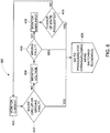
FIG. 5 in describing amethod 280 of opening/closing switching system 70. Initially, a decision is reached inCPU 204 to change a position of switchingsystem 70 as indicated inblock 300. At this point,CPU 204 checks the readiness ofHALT circuit 190 inblock 302. IfHALT circuit 190 is ready,primary HALT switch 196 is closed as indicated inblock 304. IfHALT circuit 190 is not ready, secondary HALT switch 197 is closed as indicated inblock 306. By ready it should be understood that if voltage is not above a predetermined threshold, the HALT circuit will not posses enough energy to activate the circuit breaker device and provide protection. In such a case, a different HALT circuit may be employed, or there may be a pause to allow the HALT circuit time to re-energize. At this point, the HALT switch on the associated MEMS circuit board is closed as indicated inblock 308. HALT current flows to the diode bridge on the MEMS circuit board as indicate inblock 310. At this point, a determination is made whether to open or close the switching system inblock 320. If closing the switching system,CPU 204 passes a signal through one of the first and second control busses 30 and 31 to the gate drivers on the associated MEMS circuit breaker device causing the MEMS switches to change position and pass electrical current as indicated inblock 322. If opening the switching system,CPU 204 cuts off the signal through one of the first and second control busses 30 and 31 to the gate drivers on the associated MEMS circuit breaker device causing the MEMS switches to change position and open thereby interrupting current flow through the associated MEMS circuit breaker device as indicated inblock 324. - Reference will now be made to
FIG. 6 in describing amethod 380 of deciding to open a switch assembly in accordance with an example embodiment. Initially, current passing through the switch assembly is monitored as indicated inblock 400.Current sensing module 211 monitors for a short circuit and GFCI module monitors for a ground fault as indicated inblock 402. If no short circuit or ground fault is found, voltage is monitored as indicated inblock 404 andAFCI module 209 monitors for arc faults inblock 406.CPU 204 also monitors for user input inblock 408. If a change of state is requested as shown onblock 410, or if a short circuit, ground fault, or arc fault is detected inblocks method 280 is initiated to open the switch assembly as indicated inblock 420 to protect the branch circuit associated with the affected MEMS circuit breaker. - At this point it should be understood that the present invention provides a system that utilizes MEMS devices to pass and/or interrupt current between electrical mains and branch circuits. The MEMS devices are controlled by a MEMS control board that monitors current and voltage. In the event of a current or voltage fault, the MEMS control board signals the MEMS device(s) to open and interrupt current flow. The use of a MEMS control board removes the need to provide dedicated ground fault, arc fault and short circuit monitoring at each circuit breaker. In addition, the use of MEMS devices will lead to a size and cost reduction for each circuit breaker. It should be also understood that current and voltage ratings for each MEMS device can vary based on a particular circuit rating. Also, the number of MEMS devices/dies used in a particular MEMS circuit breaker can also vary. In addition, while shown and described as an industrial/residential load center, the example embodiments can be incorporated into a wide array of electrical protection devices or systems that would benefit from circuit monitoring and protection.
- While the invention has been described in detail in connection with only a limited number of embodiments, it should be readily understood that the invention is not limited to such disclosed embodiments. Rather, the invention is not to be seen as limited by the foregoing description, but is only limited by the scope of the appended claims.
Claims (1)
- An electrical load center comprising:a main housing (16) including a plurality of walls (10, 11, 13, 14) that define an interior portion (18);the bus bar (24, 26) extending within the interior portion of the main housing; andan electrical distribution system (40) comprisingat least one circuit breaker device (49- 54, 60a- 60v) including an electrical interruption system having an electrical pathway, at least one micro-electromechanical switch (MEMS) device electrically coupled in the electrical pathway, at least one hybrid arcless limiting technology (HALT) connection, and at least one control connection;a HALT circuit (190) member electrically coupled to the HALT connection on the circuit breaker device, anda controller (44) electrically coupled to the control connection on the circuit breaker device (49- 54, 60a- 60v), the controller (44) being configured and disposed to selectively connect the HALT circuit (190) member and the at least one circuit breaker device (49- 54, 60a- 60v) via the HALT connection to control electrical current flow through the at least one circuit breaker device (49- 54, 60a- 60v),wherein the electrical load center further comprises another bus bar (24, 25) extending within the interior portion (18) of the main housing adjacent the bus bar (24, 25) and another HALT circuit member,wherein the at least one circuit breaker device (49- 54, 60a- 60v) includes a plurality of first circuit breaker devices (49- 54, 60a- 60v) electrically coupled to the bus bar (24, 25) and a plurality of second circuit breaker devices (49- 54, 60a- 60v) electrically coupled to the other bus bar (24, 25), the controller, and the another HALT circuit member.
Applications Claiming Priority (1)
| Application Number | Priority Date | Filing Date | Title |
|---|---|---|---|
| US13/172,214 US8570713B2 (en) | 2011-06-29 | 2011-06-29 | Electrical distribution system including micro electro-mechanical switch (MEMS) devices |
Publications (2)
| Publication Number | Publication Date |
|---|---|
| EP2541568A1 EP2541568A1 (en) | 2013-01-02 |
| EP2541568B1 true EP2541568B1 (en) | 2017-04-19 |
Family
ID=46507858
Family Applications (1)
| Application Number | Title | Priority Date | Filing Date |
|---|---|---|---|
| EP12173514.6A Active EP2541568B1 (en) | 2011-06-29 | 2012-06-26 | Electrical distribution system including micro electro-mechanical switch (MEMS) devices |
Country Status (4)
| Country | Link |
|---|---|
| US (1) | US8570713B2 (en) |
| EP (1) | EP2541568B1 (en) |
| JP (1) | JP6219021B2 (en) |
| CN (1) | CN102856874B (en) |
Families Citing this family (15)
| Publication number | Priority date | Publication date | Assignee | Title |
|---|---|---|---|---|
| US9825884B2 (en) | 2013-12-30 | 2017-11-21 | Cavium, Inc. | Protocol independent programmable switch (PIPS) software defined data center networks |
| US9635146B2 (en) | 2014-06-19 | 2017-04-25 | Cavium, Inc. | Method of using bit vectors to allow expansion and collapse of header layers within packets for enabling flexible modifications and an apparatus thereof |
| US9628385B2 (en) | 2014-06-19 | 2017-04-18 | Cavium, Inc. | Method of identifying internal destinations of networks packets and an apparatus thereof |
| US10616380B2 (en) | 2014-06-19 | 2020-04-07 | Cavium, Llc | Method of handling large protocol layers for configurable extraction of layer information and an apparatus thereof |
| US9742694B2 (en) * | 2014-06-19 | 2017-08-22 | Cavium, Inc. | Method of dynamically renumbering ports and an apparatus thereof |
| US10205313B2 (en) | 2015-07-24 | 2019-02-12 | Symptote Technologies, LLC | Two-transistor devices for protecting circuits from sustained overcurrent |
| US10770883B2 (en) | 2015-09-21 | 2020-09-08 | Sympote Technologies LLC | One-transistor devices for protecting circuits and autocatalytic voltage conversion therefor |
| US9997317B2 (en) | 2015-10-22 | 2018-06-12 | General Electric Company | Isolated control circuit and driver for micro-electromechanical system switch |
| US10068733B2 (en) | 2015-10-22 | 2018-09-04 | General Electric Company | Micro-electromechanical system relay circuit |
| US10083811B2 (en) | 2015-10-22 | 2018-09-25 | General Electric Company | Auxiliary circuit for micro-electromechanical system relay circuit |
| DE102016215001A1 (en) * | 2016-08-11 | 2018-02-15 | Siemens Aktiengesellschaft | Switching cell with semiconductor switching element and microelectromechanical switching element |
| GB2564434B (en) | 2017-07-10 | 2020-08-26 | Ge Aviat Systems Ltd | Power distribution switch for a power distribution system |
| DE102019211460A1 (en) * | 2019-07-31 | 2021-02-04 | Siemens Aktiengesellschaft | Arrangement of MEMS switches |
| GB2587810B (en) | 2019-10-02 | 2022-04-06 | Siemens Ag | Subsea Connector |
| US20210359498A1 (en) * | 2020-05-15 | 2021-11-18 | Rosendin Electric, Inc. | Modular electrical power distribution panel |
Family Cites Families (13)
| Publication number | Priority date | Publication date | Assignee | Title |
|---|---|---|---|---|
| US7542250B2 (en) | 2007-01-10 | 2009-06-02 | General Electric Company | Micro-electromechanical system based electric motor starter |
| US8144445B2 (en) | 2007-06-12 | 2012-03-27 | General Electric Company | Micro-electromechanical system based switching |
| US20080310058A1 (en) | 2007-06-15 | 2008-12-18 | General Electric Company | Mems micro-switch array based current limiting arc-flash eliminator |
| US8358488B2 (en) * | 2007-06-15 | 2013-01-22 | General Electric Company | Micro-electromechanical system based switching |
| US7612971B2 (en) | 2007-06-15 | 2009-11-03 | General Electric Company | Micro-electromechanical system based switching in heating-ventilation-air-conditioning systems |
| US7885043B2 (en) | 2007-06-15 | 2011-02-08 | General Electric Company | Remote-operable micro-electromechanical system based over-current protection apparatus |
| US7589942B2 (en) | 2007-06-15 | 2009-09-15 | General Electric Company | MEMS based motor starter with motor failure detection |
| US7903382B2 (en) | 2007-06-19 | 2011-03-08 | General Electric Company | MEMS micro-switch array based on current limiting enabled circuit interrupting apparatus |
| US20090161277A1 (en) | 2007-12-21 | 2009-06-25 | Robert Roesner | Method and device for preventing damage to a semiconductor switch circuit during a failure |
| US8687325B2 (en) * | 2008-09-11 | 2014-04-01 | General Electric Company | Micro-electromechanical switch protection in series parallel topology |
| US8054589B2 (en) | 2009-12-16 | 2011-11-08 | General Electric Company | Switch structure and associated circuit |
| US8547684B2 (en) | 2009-12-17 | 2013-10-01 | Schneider Electric USA, Inc. | Panelboard having a parallel feeder bars distribution |
| US8350509B2 (en) * | 2011-01-04 | 2013-01-08 | General Electric Company | Power switching system including a micro-electromechanical system (MEMS) array |
-
2011
- 2011-06-29 US US13/172,214 patent/US8570713B2/en active Active
-
2012
- 2012-06-25 JP JP2012141543A patent/JP6219021B2/en active Active
- 2012-06-26 EP EP12173514.6A patent/EP2541568B1/en active Active
- 2012-06-29 CN CN201210220567.0A patent/CN102856874B/en active Active
Non-Patent Citations (1)
| Title |
|---|
| None * |
Also Published As
| Publication number | Publication date |
|---|---|
| JP2013013310A (en) | 2013-01-17 |
| JP6219021B2 (en) | 2017-10-25 |
| US8570713B2 (en) | 2013-10-29 |
| CN102856874A (en) | 2013-01-02 |
| EP2541568A1 (en) | 2013-01-02 |
| CN102856874B (en) | 2016-12-21 |
| US20130003262A1 (en) | 2013-01-03 |
Similar Documents
| Publication | Publication Date | Title |
|---|---|---|
| EP2541568B1 (en) | Electrical distribution system including micro electro-mechanical switch (MEMS) devices | |
| JP5255630B2 (en) | Micro-electromechanical system based switching in heating, ventilation and air conditioning systems | |
| JP5284352B2 (en) | Switching using microelectromechanical systems | |
| KR101492659B1 (en) | Mems micro-switch array based on current limiting enabled circuit interrupting apparatus | |
| JP5364699B2 (en) | Overcurrent protection device using a microelectromechanical system that can be operated remotely | |
| EP2162896B1 (en) | Micro-electromechanical system based selectively coordinated protection systems and methods for electrical distribution | |
| KR101415456B1 (en) | Resettable mems micro-switch array based on current limiting apparatus | |
| KR20120079452A (en) | Power switching system including a micro-electromechanical system(mems) array |
Legal Events
| Date | Code | Title | Description |
|---|---|---|---|
| PUAI | Public reference made under article 153(3) epc to a published international application that has entered the european phase |
Free format text: ORIGINAL CODE: 0009012 |
|
| AK | Designated contracting states |
Kind code of ref document: A1 Designated state(s): AL AT BE BG CH CY CZ DE DK EE ES FI FR GB GR HR HU IE IS IT LI LT LU LV MC MK MT NL NO PL PT RO RS SE SI SK SM TR |
|
| AX | Request for extension of the european patent |
Extension state: BA ME |
|
| 17P | Request for examination filed |
Effective date: 20130702 |
|
| RBV | Designated contracting states (corrected) |
Designated state(s): AL AT BE BG CH CY CZ DE DK EE ES FI FR GB GR HR HU IE IS IT LI LT LU LV MC MK MT NL NO PL PT RO RS SE SI SK SM TR |
|
| 17Q | First examination report despatched |
Effective date: 20151119 |
|
| GRAP | Despatch of communication of intention to grant a patent |
Free format text: ORIGINAL CODE: EPIDOSNIGR1 |
|
| INTG | Intention to grant announced |
Effective date: 20161111 |
|
| GRAS | Grant fee paid |
Free format text: ORIGINAL CODE: EPIDOSNIGR3 |
|
| GRAA | (expected) grant |
Free format text: ORIGINAL CODE: 0009210 |
|
| AK | Designated contracting states |
Kind code of ref document: B1 Designated state(s): AL AT BE BG CH CY CZ DE DK EE ES FI FR GB GR HR HU IE IS IT LI LT LU LV MC MK MT NL NO PL PT RO RS SE SI SK SM TR |
|
| REG | Reference to a national code |
Ref country code: GB Ref legal event code: FG4D |
|
| REG | Reference to a national code |
Ref country code: CH Ref legal event code: EP |
|
| REG | Reference to a national code |
Ref country code: AT Ref legal event code: REF Ref document number: 886663 Country of ref document: AT Kind code of ref document: T Effective date: 20170515 |
|
| REG | Reference to a national code |
Ref country code: IE Ref legal event code: FG4D |
|
| REG | Reference to a national code |
Ref country code: DE Ref legal event code: R096 Ref document number: 602012031252 Country of ref document: DE |
|
| REG | Reference to a national code |
Ref country code: NL Ref legal event code: MP Effective date: 20170419 |
|
| REG | Reference to a national code |
Ref country code: LT Ref legal event code: MG4D |
|
| REG | Reference to a national code |
Ref country code: AT Ref legal event code: MK05 Ref document number: 886663 Country of ref document: AT Kind code of ref document: T Effective date: 20170419 |
|
| PG25 | Lapsed in a contracting state [announced via postgrant information from national office to epo] |
Ref country code: NL Free format text: LAPSE BECAUSE OF FAILURE TO SUBMIT A TRANSLATION OF THE DESCRIPTION OR TO PAY THE FEE WITHIN THE PRESCRIBED TIME-LIMIT Effective date: 20170419 |
|
| PG25 | Lapsed in a contracting state [announced via postgrant information from national office to epo] |
Ref country code: ES Free format text: LAPSE BECAUSE OF FAILURE TO SUBMIT A TRANSLATION OF THE DESCRIPTION OR TO PAY THE FEE WITHIN THE PRESCRIBED TIME-LIMIT Effective date: 20170419 Ref country code: GR Free format text: LAPSE BECAUSE OF FAILURE TO SUBMIT A TRANSLATION OF THE DESCRIPTION OR TO PAY THE FEE WITHIN THE PRESCRIBED TIME-LIMIT Effective date: 20170720 Ref country code: FI Free format text: LAPSE BECAUSE OF FAILURE TO SUBMIT A TRANSLATION OF THE DESCRIPTION OR TO PAY THE FEE WITHIN THE PRESCRIBED TIME-LIMIT Effective date: 20170419 Ref country code: AT Free format text: LAPSE BECAUSE OF FAILURE TO SUBMIT A TRANSLATION OF THE DESCRIPTION OR TO PAY THE FEE WITHIN THE PRESCRIBED TIME-LIMIT Effective date: 20170419 Ref country code: HR Free format text: LAPSE BECAUSE OF FAILURE TO SUBMIT A TRANSLATION OF THE DESCRIPTION OR TO PAY THE FEE WITHIN THE PRESCRIBED TIME-LIMIT Effective date: 20170419 Ref country code: LT Free format text: LAPSE BECAUSE OF FAILURE TO SUBMIT A TRANSLATION OF THE DESCRIPTION OR TO PAY THE FEE WITHIN THE PRESCRIBED TIME-LIMIT Effective date: 20170419 Ref country code: NO Free format text: LAPSE BECAUSE OF FAILURE TO SUBMIT A TRANSLATION OF THE DESCRIPTION OR TO PAY THE FEE WITHIN THE PRESCRIBED TIME-LIMIT Effective date: 20170719 |
|
| PG25 | Lapsed in a contracting state [announced via postgrant information from national office to epo] |
Ref country code: IS Free format text: LAPSE BECAUSE OF FAILURE TO SUBMIT A TRANSLATION OF THE DESCRIPTION OR TO PAY THE FEE WITHIN THE PRESCRIBED TIME-LIMIT Effective date: 20170819 Ref country code: SE Free format text: LAPSE BECAUSE OF FAILURE TO SUBMIT A TRANSLATION OF THE DESCRIPTION OR TO PAY THE FEE WITHIN THE PRESCRIBED TIME-LIMIT Effective date: 20170419 Ref country code: PL Free format text: LAPSE BECAUSE OF FAILURE TO SUBMIT A TRANSLATION OF THE DESCRIPTION OR TO PAY THE FEE WITHIN THE PRESCRIBED TIME-LIMIT Effective date: 20170419 Ref country code: LV Free format text: LAPSE BECAUSE OF FAILURE TO SUBMIT A TRANSLATION OF THE DESCRIPTION OR TO PAY THE FEE WITHIN THE PRESCRIBED TIME-LIMIT Effective date: 20170419 Ref country code: BG Free format text: LAPSE BECAUSE OF FAILURE TO SUBMIT A TRANSLATION OF THE DESCRIPTION OR TO PAY THE FEE WITHIN THE PRESCRIBED TIME-LIMIT Effective date: 20170719 Ref country code: RS Free format text: LAPSE BECAUSE OF FAILURE TO SUBMIT A TRANSLATION OF THE DESCRIPTION OR TO PAY THE FEE WITHIN THE PRESCRIBED TIME-LIMIT Effective date: 20170419 |
|
| REG | Reference to a national code |
Ref country code: DE Ref legal event code: R097 Ref document number: 602012031252 Country of ref document: DE |
|
| PG25 | Lapsed in a contracting state [announced via postgrant information from national office to epo] |
Ref country code: DK Free format text: LAPSE BECAUSE OF FAILURE TO SUBMIT A TRANSLATION OF THE DESCRIPTION OR TO PAY THE FEE WITHIN THE PRESCRIBED TIME-LIMIT Effective date: 20170419 Ref country code: SK Free format text: LAPSE BECAUSE OF FAILURE TO SUBMIT A TRANSLATION OF THE DESCRIPTION OR TO PAY THE FEE WITHIN THE PRESCRIBED TIME-LIMIT Effective date: 20170419 Ref country code: MC Free format text: LAPSE BECAUSE OF FAILURE TO SUBMIT A TRANSLATION OF THE DESCRIPTION OR TO PAY THE FEE WITHIN THE PRESCRIBED TIME-LIMIT Effective date: 20170419 Ref country code: RO Free format text: LAPSE BECAUSE OF FAILURE TO SUBMIT A TRANSLATION OF THE DESCRIPTION OR TO PAY THE FEE WITHIN THE PRESCRIBED TIME-LIMIT Effective date: 20170419 Ref country code: EE Free format text: LAPSE BECAUSE OF FAILURE TO SUBMIT A TRANSLATION OF THE DESCRIPTION OR TO PAY THE FEE WITHIN THE PRESCRIBED TIME-LIMIT Effective date: 20170419 Ref country code: CZ Free format text: LAPSE BECAUSE OF FAILURE TO SUBMIT A TRANSLATION OF THE DESCRIPTION OR TO PAY THE FEE WITHIN THE PRESCRIBED TIME-LIMIT Effective date: 20170419 |
|
| REG | Reference to a national code |
Ref country code: CH Ref legal event code: PL |
|
| PLBE | No opposition filed within time limit |
Free format text: ORIGINAL CODE: 0009261 |
|
| STAA | Information on the status of an ep patent application or granted ep patent |
Free format text: STATUS: NO OPPOSITION FILED WITHIN TIME LIMIT |
|
| PG25 | Lapsed in a contracting state [announced via postgrant information from national office to epo] |
Ref country code: IT Free format text: LAPSE BECAUSE OF FAILURE TO SUBMIT A TRANSLATION OF THE DESCRIPTION OR TO PAY THE FEE WITHIN THE PRESCRIBED TIME-LIMIT Effective date: 20170419 Ref country code: SM Free format text: LAPSE BECAUSE OF FAILURE TO SUBMIT A TRANSLATION OF THE DESCRIPTION OR TO PAY THE FEE WITHIN THE PRESCRIBED TIME-LIMIT Effective date: 20170419 |
|
| REG | Reference to a national code |
Ref country code: IE Ref legal event code: MM4A |
|
| 26N | No opposition filed |
Effective date: 20180122 |
|
| GBPC | Gb: european patent ceased through non-payment of renewal fee |
Effective date: 20170719 |
|
| REG | Reference to a national code |
Ref country code: FR Ref legal event code: ST Effective date: 20180228 |
|
| PG25 | Lapsed in a contracting state [announced via postgrant information from national office to epo] |
Ref country code: IE Free format text: LAPSE BECAUSE OF NON-PAYMENT OF DUE FEES Effective date: 20170626 Ref country code: GB Free format text: LAPSE BECAUSE OF NON-PAYMENT OF DUE FEES Effective date: 20170719 Ref country code: CH Free format text: LAPSE BECAUSE OF NON-PAYMENT OF DUE FEES Effective date: 20170630 Ref country code: LI Free format text: LAPSE BECAUSE OF NON-PAYMENT OF DUE FEES Effective date: 20170630 Ref country code: LU Free format text: LAPSE BECAUSE OF NON-PAYMENT OF DUE FEES Effective date: 20170626 |
|
| PG25 | Lapsed in a contracting state [announced via postgrant information from national office to epo] |
Ref country code: SI Free format text: LAPSE BECAUSE OF FAILURE TO SUBMIT A TRANSLATION OF THE DESCRIPTION OR TO PAY THE FEE WITHIN THE PRESCRIBED TIME-LIMIT Effective date: 20170419 Ref country code: FR Free format text: LAPSE BECAUSE OF NON-PAYMENT OF DUE FEES Effective date: 20170630 |
|
| REG | Reference to a national code |
Ref country code: BE Ref legal event code: MM Effective date: 20170630 |
|
| PG25 | Lapsed in a contracting state [announced via postgrant information from national office to epo] |
Ref country code: BE Free format text: LAPSE BECAUSE OF NON-PAYMENT OF DUE FEES Effective date: 20170630 |
|
| PG25 | Lapsed in a contracting state [announced via postgrant information from national office to epo] |
Ref country code: MT Free format text: LAPSE BECAUSE OF NON-PAYMENT OF DUE FEES Effective date: 20170626 |
|
| PG25 | Lapsed in a contracting state [announced via postgrant information from national office to epo] |
Ref country code: HU Free format text: LAPSE BECAUSE OF FAILURE TO SUBMIT A TRANSLATION OF THE DESCRIPTION OR TO PAY THE FEE WITHIN THE PRESCRIBED TIME-LIMIT; INVALID AB INITIO Effective date: 20120626 |
|
| PG25 | Lapsed in a contracting state [announced via postgrant information from national office to epo] |
Ref country code: CY Free format text: LAPSE BECAUSE OF NON-PAYMENT OF DUE FEES Effective date: 20170419 |
|
| PG25 | Lapsed in a contracting state [announced via postgrant information from national office to epo] |
Ref country code: MK Free format text: LAPSE BECAUSE OF FAILURE TO SUBMIT A TRANSLATION OF THE DESCRIPTION OR TO PAY THE FEE WITHIN THE PRESCRIBED TIME-LIMIT Effective date: 20170419 |
|
| PG25 | Lapsed in a contracting state [announced via postgrant information from national office to epo] |
Ref country code: TR Free format text: LAPSE BECAUSE OF FAILURE TO SUBMIT A TRANSLATION OF THE DESCRIPTION OR TO PAY THE FEE WITHIN THE PRESCRIBED TIME-LIMIT Effective date: 20170419 |
|
| PG25 | Lapsed in a contracting state [announced via postgrant information from national office to epo] |
Ref country code: PT Free format text: LAPSE BECAUSE OF FAILURE TO SUBMIT A TRANSLATION OF THE DESCRIPTION OR TO PAY THE FEE WITHIN THE PRESCRIBED TIME-LIMIT Effective date: 20170419 |
|
| PG25 | Lapsed in a contracting state [announced via postgrant information from national office to epo] |
Ref country code: AL Free format text: LAPSE BECAUSE OF FAILURE TO SUBMIT A TRANSLATION OF THE DESCRIPTION OR TO PAY THE FEE WITHIN THE PRESCRIBED TIME-LIMIT Effective date: 20170419 |
|
| REG | Reference to a national code |
Ref country code: DE Ref legal event code: R081 Ref document number: 602012031252 Country of ref document: DE Owner name: ABB SCHWEIZ AG, CH Free format text: FORMER OWNER: GENERAL ELECTRIC CO., SCHENECTADY, N.Y., US |
|
| PGFP | Annual fee paid to national office [announced via postgrant information from national office to epo] |
Ref country code: DE Payment date: 20230620 Year of fee payment: 12 |