EP2541317A2 - Display apparatus for controlling optical transmissivity - Google Patents
Display apparatus for controlling optical transmissivity Download PDFInfo
- Publication number
- EP2541317A2 EP2541317A2 EP20120159170 EP12159170A EP2541317A2 EP 2541317 A2 EP2541317 A2 EP 2541317A2 EP 20120159170 EP20120159170 EP 20120159170 EP 12159170 A EP12159170 A EP 12159170A EP 2541317 A2 EP2541317 A2 EP 2541317A2
- Authority
- EP
- European Patent Office
- Prior art keywords
- phase
- external light
- retarder
- display apparatus
- polarizer
- Prior art date
- Legal status (The legal status is an assumption and is not a legal conclusion. Google has not performed a legal analysis and makes no representation as to the accuracy of the status listed.)
- Granted
Links
Images


Classifications
-
- G—PHYSICS
- G02—OPTICS
- G02F—OPTICAL DEVICES OR ARRANGEMENTS FOR THE CONTROL OF LIGHT BY MODIFICATION OF THE OPTICAL PROPERTIES OF THE MEDIA OF THE ELEMENTS INVOLVED THEREIN; NON-LINEAR OPTICS; FREQUENCY-CHANGING OF LIGHT; OPTICAL LOGIC ELEMENTS; OPTICAL ANALOGUE/DIGITAL CONVERTERS
- G02F1/00—Devices or arrangements for the control of the intensity, colour, phase, polarisation or direction of light arriving from an independent light source, e.g. switching, gating or modulating; Non-linear optics
- G02F1/01—Devices or arrangements for the control of the intensity, colour, phase, polarisation or direction of light arriving from an independent light source, e.g. switching, gating or modulating; Non-linear optics for the control of the intensity, phase, polarisation or colour
- G02F1/13—Devices or arrangements for the control of the intensity, colour, phase, polarisation or direction of light arriving from an independent light source, e.g. switching, gating or modulating; Non-linear optics for the control of the intensity, phase, polarisation or colour based on liquid crystals, e.g. single liquid crystal display cells
- G02F1/133—Constructional arrangements; Operation of liquid crystal cells; Circuit arrangements
- G02F1/136—Liquid crystal cells structurally associated with a semi-conducting layer or substrate, e.g. cells forming part of an integrated circuit
- G02F1/1362—Active matrix addressed cells
-
- G—PHYSICS
- G02—OPTICS
- G02B—OPTICAL ELEMENTS, SYSTEMS OR APPARATUS
- G02B5/00—Optical elements other than lenses
- G02B5/30—Polarising elements
- G02B5/3025—Polarisers, i.e. arrangements capable of producing a definite output polarisation state from an unpolarised input state
-
- G—PHYSICS
- G02—OPTICS
- G02F—OPTICAL DEVICES OR ARRANGEMENTS FOR THE CONTROL OF LIGHT BY MODIFICATION OF THE OPTICAL PROPERTIES OF THE MEDIA OF THE ELEMENTS INVOLVED THEREIN; NON-LINEAR OPTICS; FREQUENCY-CHANGING OF LIGHT; OPTICAL LOGIC ELEMENTS; OPTICAL ANALOGUE/DIGITAL CONVERTERS
- G02F1/00—Devices or arrangements for the control of the intensity, colour, phase, polarisation or direction of light arriving from an independent light source, e.g. switching, gating or modulating; Non-linear optics
- G02F1/01—Devices or arrangements for the control of the intensity, colour, phase, polarisation or direction of light arriving from an independent light source, e.g. switching, gating or modulating; Non-linear optics for the control of the intensity, phase, polarisation or colour
- G02F1/13—Devices or arrangements for the control of the intensity, colour, phase, polarisation or direction of light arriving from an independent light source, e.g. switching, gating or modulating; Non-linear optics for the control of the intensity, phase, polarisation or colour based on liquid crystals, e.g. single liquid crystal display cells
- G02F1/133—Constructional arrangements; Operation of liquid crystal cells; Circuit arrangements
- G02F1/1333—Constructional arrangements; Manufacturing methods
- G02F1/133345—Insulating layers
-
- G—PHYSICS
- G02—OPTICS
- G02F—OPTICAL DEVICES OR ARRANGEMENTS FOR THE CONTROL OF LIGHT BY MODIFICATION OF THE OPTICAL PROPERTIES OF THE MEDIA OF THE ELEMENTS INVOLVED THEREIN; NON-LINEAR OPTICS; FREQUENCY-CHANGING OF LIGHT; OPTICAL LOGIC ELEMENTS; OPTICAL ANALOGUE/DIGITAL CONVERTERS
- G02F1/00—Devices or arrangements for the control of the intensity, colour, phase, polarisation or direction of light arriving from an independent light source, e.g. switching, gating or modulating; Non-linear optics
- G02F1/01—Devices or arrangements for the control of the intensity, colour, phase, polarisation or direction of light arriving from an independent light source, e.g. switching, gating or modulating; Non-linear optics for the control of the intensity, phase, polarisation or colour
- G02F1/13—Devices or arrangements for the control of the intensity, colour, phase, polarisation or direction of light arriving from an independent light source, e.g. switching, gating or modulating; Non-linear optics for the control of the intensity, phase, polarisation or colour based on liquid crystals, e.g. single liquid crystal display cells
- G02F1/133—Constructional arrangements; Operation of liquid crystal cells; Circuit arrangements
- G02F1/1333—Constructional arrangements; Manufacturing methods
- G02F1/1335—Structural association of cells with optical devices, e.g. polarisers or reflectors
- G02F1/133528—Polarisers
-
- G—PHYSICS
- G02—OPTICS
- G02F—OPTICAL DEVICES OR ARRANGEMENTS FOR THE CONTROL OF LIGHT BY MODIFICATION OF THE OPTICAL PROPERTIES OF THE MEDIA OF THE ELEMENTS INVOLVED THEREIN; NON-LINEAR OPTICS; FREQUENCY-CHANGING OF LIGHT; OPTICAL LOGIC ELEMENTS; OPTICAL ANALOGUE/DIGITAL CONVERTERS
- G02F1/00—Devices or arrangements for the control of the intensity, colour, phase, polarisation or direction of light arriving from an independent light source, e.g. switching, gating or modulating; Non-linear optics
- G02F1/01—Devices or arrangements for the control of the intensity, colour, phase, polarisation or direction of light arriving from an independent light source, e.g. switching, gating or modulating; Non-linear optics for the control of the intensity, phase, polarisation or colour
- G02F1/13—Devices or arrangements for the control of the intensity, colour, phase, polarisation or direction of light arriving from an independent light source, e.g. switching, gating or modulating; Non-linear optics for the control of the intensity, phase, polarisation or colour based on liquid crystals, e.g. single liquid crystal display cells
- G02F1/133—Constructional arrangements; Operation of liquid crystal cells; Circuit arrangements
- G02F1/1333—Constructional arrangements; Manufacturing methods
- G02F1/1335—Structural association of cells with optical devices, e.g. polarisers or reflectors
- G02F1/1336—Illuminating devices
- G02F1/13362—Illuminating devices providing polarized light, e.g. by converting a polarisation component into another one
-
- G—PHYSICS
- G02—OPTICS
- G02F—OPTICAL DEVICES OR ARRANGEMENTS FOR THE CONTROL OF LIGHT BY MODIFICATION OF THE OPTICAL PROPERTIES OF THE MEDIA OF THE ELEMENTS INVOLVED THEREIN; NON-LINEAR OPTICS; FREQUENCY-CHANGING OF LIGHT; OPTICAL LOGIC ELEMENTS; OPTICAL ANALOGUE/DIGITAL CONVERTERS
- G02F1/00—Devices or arrangements for the control of the intensity, colour, phase, polarisation or direction of light arriving from an independent light source, e.g. switching, gating or modulating; Non-linear optics
- G02F1/01—Devices or arrangements for the control of the intensity, colour, phase, polarisation or direction of light arriving from an independent light source, e.g. switching, gating or modulating; Non-linear optics for the control of the intensity, phase, polarisation or colour
- G02F1/13—Devices or arrangements for the control of the intensity, colour, phase, polarisation or direction of light arriving from an independent light source, e.g. switching, gating or modulating; Non-linear optics for the control of the intensity, phase, polarisation or colour based on liquid crystals, e.g. single liquid crystal display cells
- G02F1/133—Constructional arrangements; Operation of liquid crystal cells; Circuit arrangements
- G02F1/1333—Constructional arrangements; Manufacturing methods
- G02F1/1335—Structural association of cells with optical devices, e.g. polarisers or reflectors
- G02F1/13363—Birefringent elements, e.g. for optical compensation
-
- G—PHYSICS
- G02—OPTICS
- G02F—OPTICAL DEVICES OR ARRANGEMENTS FOR THE CONTROL OF LIGHT BY MODIFICATION OF THE OPTICAL PROPERTIES OF THE MEDIA OF THE ELEMENTS INVOLVED THEREIN; NON-LINEAR OPTICS; FREQUENCY-CHANGING OF LIGHT; OPTICAL LOGIC ELEMENTS; OPTICAL ANALOGUE/DIGITAL CONVERTERS
- G02F1/00—Devices or arrangements for the control of the intensity, colour, phase, polarisation or direction of light arriving from an independent light source, e.g. switching, gating or modulating; Non-linear optics
- G02F1/01—Devices or arrangements for the control of the intensity, colour, phase, polarisation or direction of light arriving from an independent light source, e.g. switching, gating or modulating; Non-linear optics for the control of the intensity, phase, polarisation or colour
- G02F1/13—Devices or arrangements for the control of the intensity, colour, phase, polarisation or direction of light arriving from an independent light source, e.g. switching, gating or modulating; Non-linear optics for the control of the intensity, phase, polarisation or colour based on liquid crystals, e.g. single liquid crystal display cells
- G02F1/133—Constructional arrangements; Operation of liquid crystal cells; Circuit arrangements
- G02F1/136—Liquid crystal cells structurally associated with a semi-conducting layer or substrate, e.g. cells forming part of an integrated circuit
- G02F1/1362—Active matrix addressed cells
- G02F1/1368—Active matrix addressed cells in which the switching element is a three-electrode device
-
- H—ELECTRICITY
- H10—SEMICONDUCTOR DEVICES; ELECTRIC SOLID-STATE DEVICES NOT OTHERWISE PROVIDED FOR
- H10K—ORGANIC ELECTRIC SOLID-STATE DEVICES
- H10K50/00—Organic light-emitting devices
- H10K50/80—Constructional details
- H10K50/86—Arrangements for improving contrast, e.g. preventing reflection of ambient light
-
- H—ELECTRICITY
- H10—SEMICONDUCTOR DEVICES; ELECTRIC SOLID-STATE DEVICES NOT OTHERWISE PROVIDED FOR
- H10K—ORGANIC ELECTRIC SOLID-STATE DEVICES
- H10K59/00—Integrated devices, or assemblies of multiple devices, comprising at least one organic light-emitting element covered by group H10K50/00
- H10K59/10—OLED displays
- H10K59/12—Active-matrix OLED [AMOLED] displays
- H10K59/121—Active-matrix OLED [AMOLED] displays characterised by the geometry or disposition of pixel elements
-
- H—ELECTRICITY
- H10—SEMICONDUCTOR DEVICES; ELECTRIC SOLID-STATE DEVICES NOT OTHERWISE PROVIDED FOR
- H10K—ORGANIC ELECTRIC SOLID-STATE DEVICES
- H10K59/00—Integrated devices, or assemblies of multiple devices, comprising at least one organic light-emitting element covered by group H10K50/00
- H10K59/50—OLEDs integrated with light modulating elements, e.g. with electrochromic elements, photochromic elements or liquid crystal elements
-
- H—ELECTRICITY
- H10—SEMICONDUCTOR DEVICES; ELECTRIC SOLID-STATE DEVICES NOT OTHERWISE PROVIDED FOR
- H10K—ORGANIC ELECTRIC SOLID-STATE DEVICES
- H10K59/00—Integrated devices, or assemblies of multiple devices, comprising at least one organic light-emitting element covered by group H10K50/00
- H10K59/80—Constructional details
- H10K59/8791—Arrangements for improving contrast, e.g. preventing reflection of ambient light
-
- G—PHYSICS
- G02—OPTICS
- G02F—OPTICAL DEVICES OR ARRANGEMENTS FOR THE CONTROL OF LIGHT BY MODIFICATION OF THE OPTICAL PROPERTIES OF THE MEDIA OF THE ELEMENTS INVOLVED THEREIN; NON-LINEAR OPTICS; FREQUENCY-CHANGING OF LIGHT; OPTICAL LOGIC ELEMENTS; OPTICAL ANALOGUE/DIGITAL CONVERTERS
- G02F1/00—Devices or arrangements for the control of the intensity, colour, phase, polarisation or direction of light arriving from an independent light source, e.g. switching, gating or modulating; Non-linear optics
- G02F1/01—Devices or arrangements for the control of the intensity, colour, phase, polarisation or direction of light arriving from an independent light source, e.g. switching, gating or modulating; Non-linear optics for the control of the intensity, phase, polarisation or colour
- G02F1/13—Devices or arrangements for the control of the intensity, colour, phase, polarisation or direction of light arriving from an independent light source, e.g. switching, gating or modulating; Non-linear optics for the control of the intensity, phase, polarisation or colour based on liquid crystals, e.g. single liquid crystal display cells
- G02F1/133—Constructional arrangements; Operation of liquid crystal cells; Circuit arrangements
- G02F1/1333—Constructional arrangements; Manufacturing methods
- G02F1/1335—Structural association of cells with optical devices, e.g. polarisers or reflectors
- G02F1/133528—Polarisers
- G02F1/133531—Polarisers characterised by the arrangement of polariser or analyser axes
-
- H—ELECTRICITY
- H10—SEMICONDUCTOR DEVICES; ELECTRIC SOLID-STATE DEVICES NOT OTHERWISE PROVIDED FOR
- H10K—ORGANIC ELECTRIC SOLID-STATE DEVICES
- H10K59/00—Integrated devices, or assemblies of multiple devices, comprising at least one organic light-emitting element covered by group H10K50/00
-
- H—ELECTRICITY
- H10—SEMICONDUCTOR DEVICES; ELECTRIC SOLID-STATE DEVICES NOT OTHERWISE PROVIDED FOR
- H10K—ORGANIC ELECTRIC SOLID-STATE DEVICES
- H10K59/00—Integrated devices, or assemblies of multiple devices, comprising at least one organic light-emitting element covered by group H10K50/00
- H10K59/80—Constructional details
- H10K59/805—Electrodes
- H10K59/8052—Cathodes
-
- H—ELECTRICITY
- H10—SEMICONDUCTOR DEVICES; ELECTRIC SOLID-STATE DEVICES NOT OTHERWISE PROVIDED FOR
- H10K—ORGANIC ELECTRIC SOLID-STATE DEVICES
- H10K59/00—Integrated devices, or assemblies of multiple devices, comprising at least one organic light-emitting element covered by group H10K50/00
- H10K59/80—Constructional details
- H10K59/87—Passivation; Containers; Encapsulations
-
- H—ELECTRICITY
- H10—SEMICONDUCTOR DEVICES; ELECTRIC SOLID-STATE DEVICES NOT OTHERWISE PROVIDED FOR
- H10K—ORGANIC ELECTRIC SOLID-STATE DEVICES
- H10K59/00—Integrated devices, or assemblies of multiple devices, comprising at least one organic light-emitting element covered by group H10K50/00
- H10K59/80—Constructional details
- H10K59/8793—Arrangements for polarized light emission
Definitions
- the present invention relates to a display apparatus, and more particularly, to a display apparatus that has an optical transmissivity controlled according to a mode.
- Organic light-emitting display apparatuses have larger viewing angles, better contrast characteristics and faster response times, and consume less power than other types of display apparatus. Thus, organic light-emitting displays have been used in various fields of application. For example, organic light-emitting displays have been used in personal mobile devices, e.g., MP3 players and mobile phones and in TVs. An organic light-emitting display apparatus has self-light emitting characteristics, and its weight and thickness may be reduced because it does not require an additional light source, e.g., unlike a liquid crystal display (LCD) apparatus.
- LCD liquid crystal display
- an organic light-emitting display apparatus may be manufactured to be a transparent display apparatus by including transparent thin-film transistors (TFTs) or transparent organic light-emitting diodes (OLEDs) therein and by forming a transmissive region (or a transmissive window) separate from a pixel region.
- TFTs transparent thin-film transistors
- OLEDs transparent organic light-emitting diodes
- Embodiments provide a display apparatus with optical devices on a transparent display device so as to control optical transmissivity according to a mode and with a small amount of power.
- a display apparatus for controlling optical transmissivity, the display apparatus including a transparent display device, the transparent display device including a pixel divided into a first region for emitting light and a second region adjacent the first region for transmitting external light therethrough, a first polarizer on a first surface of the transparent display device, the first polarizer being configured to linearly polarize the external light and to transmit the linearly polarized light therethrough, a first retarder between the first polarizer and the first surface of the transparent display device, the first retarder being configured to delay a phase of the external light and to transmit the phase-delayed light therethrough, a second polarizer on a second surface of the transparent display device, the first and second surfaces of the transparent display device being opposite each other, and the second polarizer being configured to linearly polarize the external light and to transmit the linearly polarized light therethrough, and a conversion retarder between the second polarizer and the second surface of the transparent display device, the conversion retarder being configured to delay
- the first polarizer and the second polarizer may have the same polarizing axis.
- the first retarder may be configured to delay the wavelength of the external light by the first phase.
- the conversion retarder may be configured to delay the wavelength of the external light by the first phase in accordance with the power supplied thereto, the first and second phases having a same absolute value but different directions, and the display apparatus being configured to block transmittance of external light therethrough.
- the conversion retarder may be configured to delay the wavelength of the external light by the second phase in accordance with the power supplied thereto, the first and second phases having a same absolute value but different directions, and the display apparatus being configured to transmit external light therethrough.
- the first polarizer and the second polarizer may have polarizing axes that are perpendicular to each other.
- the first retarder may be configured to delay the wavelength of the external light by the first phase.
- the conversion retarder may be configured to delay the wavelength of the external light by the first phase in accordance with the power supplied thereto, the first and second phases having a same absolute value but different directions, and the display apparatus being configured to transmit external light therethrough.
- the conversion retarder may be configured to delay the wavelength of the external light by the second phase in accordance with the power supplied thereto, the first and second phases having a same absolute value but different directions, and the display apparatus being configured to block transmittance of external light therethrough.
- the conversion retarder may include a second retarder and a liquid crystal layer, the second retarder being between the transparent display device and the liquid crystal layer, the liquid crystal layer being between the second retarder and the second polarizer, and the liquid crystal layer being configured to delay the wavelength of the external light within the predetermined range in accordance with voltage applied thereto.
- the first polarizer and the second polarizer may have the same polarizing axis, the first retarder being configured to delay the wavelength of the external light by the first phase.
- the second retarder may be configured to delay the wavelength of the external light by the second phase
- the liquid crystal layer may be configured to delay the wavelength of the external light within a range from a third phase to a fourth phase when voltage is applied to the liquid crystal layer
- a sum of the third phase and the fourth phase may be equal to the fourth phase
- a sum of the fourth phase and the second phase may be equal to the first phase
- the first phase and the second phase may have a same absolute value but different directions.
- the second retarder may be configured to delay the wavelength of the external light by the first phase
- the liquid crystal layer may be configured to delay the wavelength of the external light within a range from a fifth phase to a sixth phase when voltage is applied to the liquid crystal layer
- a sum of the fifth phase and the first phase may be equal to the second phase
- a sum of the sixth phase and the first phase may be equal to the first phase
- the first phase and the second phase may have a same absolute value but different directions.
- the first polarizer and the second polarizer may have polarizing axes perpendicular to each other, the first retarder being configured to delay the wavelength of the external light by the first phase.
- the pixel may include a pixel circuit unit in the first region and including at least one thin-film transistor (TFT), a first insulating layer covering at least the pixel circuit unit, a second electrode on the first insulating layer to be electrically connected to the pixel circuit unit, the second electrode being located in the first region, a second electrode in at least the first region of the pixel and facing the first electrode, and an organic layer between the first electrode and the second electrode, the organic layer including an emission layer.
- TFT thin-film transistor
- the second electrode may include a first aperture in a location thereof corresponding to the second region.
- the display apparatus may further include a plurality of second insulating layers at a location corresponding to the second region.
- Each of the plurality of second insulating layers may include a second aperture in a location corresponding to at least a portion of the second region.
- the first insulating layer and the plurality of second insulating layers may be formed of a transparent material.
- the first electrode may be an optical transmissive electrode, and may overlap with the pixel circuit unit to cover the pixel circuit unit.
- the first electrode may be an optical reflective electrode, and does not overlap with the pixel circuit unit not to cover the pixel circuit unit.
- the conversion retarder may be a switchable retarder having at least two different phase states.
- the first retarder and the conversion retarder may include different materials.
- the conversion retarder may include liquid crystals.
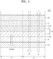
- the display apparatus 100 may include a first polarizer 21, a first retarder 41, a conversion retarder 61, and a second polarizer 22 on a transparent display device 10 that transmits external light therethrough.
- the transparent display device 10 may be a light-emitting display device that is a bottom emission type display device, and may include a first substrate 1, a display unit disposed on the first substrate 1, and a second substrate 2 that seals the display unit.
- the display unit is divided into a plurality of pixels, and each pixel includes a pixel region 31, i.e., a region for emitting light and displaying an image toward the first substrate 1, and a transmissive region 32, i.e., a region disposed adjacent to the pixel region 31 and transmitting external light therethrough.
- the first retarder 41 and the first polarizer 21 may be, e.g., sequentially, disposed at an external side, i.e., a first surface 10a, of the first substrate 1 of the transparent display device 10, i.e., a side via which light is emitted from the transparent display device 10.
- a combination of the first polarizer 21 and the first retarder 41 allows circularly polarized light, which circulates in a certain direction, to pass therethrough.
- the first polarizer 21 is a linear polarizer that linearly polarizes incident light in a certain direction
- the first retarder 41 is a switchable retarder that phase-delays incident light by +1/4 wavelength (+ ⁇ /4).
- the conversion retarder 61 and the second polarizer 22 may be, e.g., sequentially, disposed on an external side, i.e., a second surface 10b, of the second substrate 2 of the transparent display device 10, i.e., a side through which light is not emitted from the transparent display device 10. That is, the display device 10 may be between the first retarder 41 and the conversion retarder 61.
- the first retarder 41, the first substrate 1, the second substrate 2, and the conversion retarder 61 may be sequentially stacked on the first polarizer 21.
- the second polarizer 22 is a linear polarizer that linearly polarizes incident light in a certain direction.
- the first polarizer 21 and the second polarizer 22 may have the same polarizing axis. According to another embodiment, the first polarizer 21 and the second polarizer 22 may have different polarizing axes.
- the conversion retarder 61 is a switchable retarder that phase-delays incident light within a range from a (-1/4) wavelength (- ⁇ /4) to a (+1/4) wavelength +( ⁇ /4), and may change a phase-delayed value.
- the conversion retarder 61 may delay the phase of incident light according to a mode, e.g., a mode change may occur according to a voltage or power applied thereto.
- the conversion retarder 61 may be formed of liquid crystals, i.e., the liquid crystals may be arranged according to an applied electric field, or of an electrochromic material, i.e., the state of an electrochromic material may change according to power supplied thereto.
- the conversion retarder 61 when the conversion retarder 61 is formed of liquid crystals, because the liquid crystals react to a voltage difference, an even phase difference may be obtained in the entire area of the liquid crystals and the liquid crystals may be operated with a small amount of power.
- a conversion retarder 61 formed of liquid crystals may be inexpensive.
- the conversion retarder 61 of the display apparatus 100 may facilitate adjustment of transmissivity of external light with a small amount of power. That is, a phase-delayed value of the conversion retarder 61 may be controlled to adjust transmissivity with relatively low power consumption, as will be described in more detail below.
- transparent display apparatuses have a fixed transmissivity with respect to external light, and thus, a user cannot adjust the transmissivity thereof to a desired level.
- optical transmissivity may be potentially adjusted with an external controller, e.g., with a shutter installed at an outer side of the transparent display device
- use of the shutter may cause large power consumption and reduced overall transmissivity of the transparent display device.
- the shutter since the shutter includes various devices, e.g., electrodes, at least one optical film, and at least one substrate, the reduced transmissivity of the transparent display device may be relatively large, e.g., the shutter may have a transmissivity of only about 5% even in a mode for transmitting light.
- the overall transmissivity of the display device may be sharply reduced due to the shutter, thereby preventing the transparent display device from normal operation.
- the conversion retarder 61 may control phase-delayed values according to a mode.
- the transmissivity of the display device 10 may be controlled with a small amount of power, without having to use a high-power consuming optical transmissivity controller, e.g., without using a shutter.
- the optical members, e.g., polarizers and retarders, of the display apparatus 100 provide no substantial reduction of the overall transmissivity of the display device 10, e.g., unlike the shutter, thereby enabling the display apparatus 100 to perform normal operation in the transparent mode.
- a user may see through the display apparatus 100. That is, a user, at a side where an image is displayed, may view objects at an external side of the second substrate 2 by using first external light 51 transmitted in a direction from the external side of the second substrate 2 to the external side of the first substrate 1. Also, a user, at a side opposite to the side where an image is displayed, may also view an object displayed at the external side of the first substrate 1 by using second external light 52 transmitted in a direction from the external side of the first substrate 1 to the external side of the second substrate 2. The first external light 51 is transmitted in a direction in which the image is displayed, and the second external light 52 is transmitted in a direction opposite to the direction of the first external light 51.
- the display apparatus 100 operates in a black mode (or block mode) for blocking light, then a user cannot view through the display apparatus 100. That is, a user at the side where an image is displayed cannot view an object at the external side of the second substrate 2. Also, a user at the side opposite to the side where an image is displayed cannot view an object at the external side of the first substrate 1.
- Driving of the display apparatus 100 in various modes, i.e., in the transparent and black modes, will be described in detail below with reference to FIGS. 9 to 12 .
- FIG. 2 illustrates a pixel included in the transparent display device 10 of FIG. 1 according to an embodiment
- FIG. 3 illustrates a pixel included in the transparent display device 10 of FIG. 1 according to another embodiment
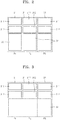
- the pixel may include a plurality of sub pixels, e.g., a red sub pixel Pr, a green sub pixel Pg, and a blue sub pixel Pb.
- Each of the red, green, and blue sub pixels Pr, Pg, and Pb includes the pixel region 31 and the transmissive region 32.
- a pixel circuit unit 311 and a light-emitting unit 312 may be disposed adjacent to each other not to overlap with each other, so that an optical path may not be blocked by the pixel circuit unit 311 when bottom emission occurs in the light-emitting unit 312 toward the first substrate 1.
- the transmissive region 32 that transmits external light therethrough may be disposed adjacent to the pixel region 31.
- the transmissive regions 32 may be disposed to respectively correspond to the red, green, and blue sub pixels Pr, Pg, and Pb to be spaced apart from each other, e.g., as illustrated in FIG.
- the pixel may include a plurality of pixel regions 31 that are disposed apart from each other between common transmissive regions 32.
- the area of the transmissive regions 32 that transmit external light therethrough in the embodiment of FIG. 3 may be larger than that in the embodiment of FIG. 2 , thereby increasing the overall transmissivity of the display unit.
- FIG. 3 illustrates that all the transmissive regions 32 corresponding to the red sub pixel Pr, the green sub pixel Pg, and the blue sub pixel Pb are connected to each other, example embodiments are not limited thereto, e.g., the transmissive regions 32 corresponding to two adjacent sub pixels from among the red sub pixel Pr, the green sub pixel Pg, and the blue sub pixel Pb may be connected to each other.
- FIG. 4 is a cross-sectional view of one of the red, green, and blue sub pixels Pr, Pg, and Pb illustrated in FIG. 2 or FIG. 3 .
- a thin-film transistor TFT
- the pixel circuit unit 311 may further include a plurality of TFTs and a storage capacitor.
- the pixel circuit unit 311 may further include a scan line, a data line, and a Vdd line connected to the plurality of TFTs and the storage capacitor.
- an organic emission device EL that is a light-emitting device may be disposed.
- the organic emission device EL may be electrically connected to the TFT of the pixel circuit unit 311.
- a buffer layer 211 may be formed on a first substrate 1, and the pixel circuit including the TFT may be formed on the buffer layer 211.
- a semiconductor active layer 212 may be formed on the buffer layer 211.
- the buffer layer 211 protects the substrate 1 from impurities and planarizes a surface of the substrate 1.
- the buffer layer 211 may be formed of any of various materials that can perform the functions described above.
- the buffer layer 21 may be formed of an inorganic material, e.g., a silicon oxide, a silicon nitride, a silicon oxynitride, an aluminum oxide, an aluminum nitride, a titanium oxide, or a titanium nitride, and/or an organic material, e.g., polyimide, polyester, or acryl.
- the buffer layer 211 is not an essential element and thus may not be formed.
- the semiconductor active layer 212 may be formed of polycrystal silicon, but is not limited thereto, e.g., may be formed of a semiconductor oxide.
- the semiconductor active layer 212 may be a G-I-Z-O layer [(In2O3)a(Ga2O3)b(ZnO)c layer], where a, b, and c are integers that respectively satisfy a ⁇ o, b ⁇ o, and c > o.
- the transmissivity of the pixel circuit unit 311 of the pixel region 31 may be improved, thereby increasing the overall transmissivity of the display unit.
- a gate insulating layer 213 may be formed on the buffer layer 211 to cover the semiconductor active layer 212, and a gate electrode 214 may be formed on the gate insulating layer 213.
- An interlayer insulating layer 215 may be formed on the gate insulating layer 213 to cover the gate electrode 214.
- a source electrode 216 and a drain electrode 217 may be formed on the interlayer insulating layer 215 to contact the semiconductor active layer 212 through contact holes, respectively.
- the structure of the TFT is not limited to the above description and any type of TFT may be employed.
- a passivation layer 218 may be formed to cover the TFT.
- the passivation layer 218 may be a single insulating layer or a plurality of insulating layers, an upper surface of which is planarized.
- the passivation layer 218 may be formed of an inorganic material and/or an organic material.
- the passivation layer 218 may be formed to cover both the pixel region 31 and the transmissive region 32, e.g., as illustrated in FIG. 4 , but is not limited thereto.
- an aperture (not shown) may be formed in a portion of the passivation layer 218 that corresponds to the transmissive region 32, so that the efficiency of the transmissive region 32 that transmits external light therethrough may be improved.
- a first electrode 221 of the organic emission device EL to be electrically connected to the TFT may be formed on the passivation layer 218 to be electrically connected to the TFT.
- a plurality of the first electrodes 221 may be disposed in an island pattern independently in units of sub pixels.
- the first electrode 221 may be disposed in the light-emitting unit 312 of the pixel region 31 not to overlap with the pixel circuit unit 311.
- a pixel-defining layer 219 formed of an organic material and/or an inorganic material, may be formed on the passivation layer 218.
- the pixel-defining layer 219 may include a third aperture 219a, e.g., so edges of the first electrode 221 are covered by the pixel-defining layer 219 and a central part of the first electrode 221 is exposed.
- the pixel-defining layer 219 may cover the pixel region 31 but is not limited thereto, e.g., the pixel-defining layer 219 may cover at least a portion of the pixel region 31, e.g., edges of the first electrode 221.
- a second aperture 219b may be formed in a portion of the pixel-defining layer 219 corresponding to the transmissive region 32, as illustrated in FIG. 4 . If the pixel-defining layer 219 is not disposed in the transmissive region 32, the efficiency of the transmissive region 32 that transmits external light therethough may be improved.
- Both the passivation layer 218 and the pixel-defining layer 219 may be formed of a transparent material.
- insulating layers e.g., the passivation layer 218 and the pixel-defining layer 219, are formed of a transparent material, the efficiency of the transparent display device 10 that transmits external light therethough may be improved.
- An organic layer 223 and a second electrode 222 may be sequentially disposed on the first electrode 221 exposed via the third aperture 219a.
- the second electrode 222 may be disposed in pixel region 31 to face the first electrode 221 and cover the organic layer 223 and the pixel-defining layer 219.
- the second electrode 222 may be formed at least in the pixel region 31, and may include a first aperture 222a in a portion thereof corresponding to the transmissive region 32, as illustrated in FIG. 4 . If the second electrode 222 is not disposed in the transmissive region 32, the efficiency of the transmissive region 32 that transmits external light therethrough may be improved.
- the first aperture 222a and the second aperture 219b may be connected to each other.
- the organic layer 223 may be a low molecular weight organic layer or a polymer organic layer. If the organic layer 223 is a low molecular weight organic layer, the organic layer 223 may be formed by stacking a hole injection layer (HIL), a hole transport layer (HTL), an emission layer (EML), an electron transport layer (ETL), and an electron injection layer (EIL) in a single structure or a composite structure. In this case, the organic layer 223 may be formed of any of various organic materials, e.g., copper phthalocyanine (CuPc), N,N'-Di(naphthalene-1-yl)-N,N'-diphenyl-benzidine (NPB), or tris-8-hydroxyquinoline aluminum (Alq3).
- the low-molecular weight organic layer may be formed, e.g., by vacuum deposition. In this case, the HIL, the HTL, the ETL, and the EIL may be common layers to red, green, and blue pixels.
- the first electrode 221 may function as an anode and the second electrode 222 may function as a cathode, or vice versa.
- the first electrode 221 may be a transparent electrode and the second electrode 222 may be a reflective electrode.
- the first electrode 221 may be formed of a transparent conductive material, e.g., ITO, IZO, ZnO, In2O3, or the like
- the second electrode 222 may be formed of, e.g., Ag, Mg, Al, Pt, Pd, Au, Ni, Nd, Ir, Cr, Li, Ca, or the like.
- the organic emission device EL may be a bottom emission type device, in which an image is displayed toward the first electrode 221.
- the second electrode 222 may be formed to an appropriate thickness sufficient not to cause a voltage drop to occur in the entire display unit. Accordingly, it may be possible to manufacture the display apparatus 100 in a large scale.
- FIG. 5 is a schematic cross-sectional view of a display apparatus 100' according to another embodiment.
- the display apparatus 100' illustrated in FIG. 5 may be a light-emitting display apparatus in which a transparent display device 10 is a top emission type display device, unlike in the display apparatus 100 of FIG. 1 .
- the display apparatus 100' may include the first retarder 41 and the first polarizer 21 sequentially disposed on the second substrate 2 of the transparent display device 10, and the conversion retarder 61 and the second polarizer 22 sequentially disposed the first substrate 1 of the transparent display device 10.
- the display apparatus 100' includes an image displayed on the external side of the second substrate 2 of the transparent display device 10.
- Other elements of the display apparatus 100' are substantially the same as those of the display apparatus 100 of FIG. 1 in terms of their functions and, thus, will not described again.
- FIG. 6 illustrates a pixel included in the transparent display device 10 of FIG. 5 according to another embodiment.
- FIG. 7 illustrates a pixel included in the transparent display device 10 of FIG. 5 according to another embodiment.
- the pixel includes a pixel circuit unit 311 and a light-emitting unit 312 disposed to overlap with each other, unlike in the pixel illustrated in FIGS. 2 and 3 . Because a top emission occurs in the light-emitting unit 312 toward the second substrate 2, the pixel circuit unit 311 and the light-emitting unit 312 may overlap with each other. In addition, because the pixel circuit unit 311 including a pixel circuit (not shown) is covered by the light-emitting unit 312, it may be possible to prevent optical interference caused by the pixel circuit.
- Other elements of the display apparatus 100' are substantially the same as those of the display apparatus 100 of FIGS. 2 or 3 in terms of their functions and, thus, will not described again.
- the transmissive regions 32 may be disposed to respectively correspond to a plurality of sub pixels Pr, Pg, and Pb to be apart from each other, e.g., as illustrated in FIG. 6 , or may be connected to each other, e.g., as illustrated in FIG. 7 .
- FIG. 8 is a cross-sectional view of one of the red, green, and blue sub pixels Pr, Pg, and Pb illustrated in FIG. 6 or 7 .
- a TFT may be disposed in the pixel circuit unit 311, and an organic emission device EL, which is a light-emitting device, may be disposed in the light-emitting unit 312'.
- the buffer layer 211 may be formed on the first substrate 1, the semiconductor active layer 212 may be formed on the buffer layer 211, and the gate insulating layer 213, the gate electrode 214, and the interlayer insulating layer 215 may be formed on the semiconductor active layer 212.
- the source electrode 216 and the drain electrode 217 may be formed on the interlayer insulating layer 215.
- the passivation layer 218, which is a type of insulating layer, may be formed to cover the TFT.
- the passivation layer 218 may cover both the pixel region 31 and the transmissive region 32, as illustrated in FIG. 8 , but is not limited thereto.
- the passivation layer 218 may include an aperture (not shown) in a portion thereof corresponding to the transmissive region 32, thereby improving the efficiency of the transmissive region 32 that transmits external light therethrough.
- a first electrode 221 of the organic emission device EL electrically connected to the TFT may be disposed on the passivation layer 218.
- the first electrode 221 may be disposed in the light-emitting unit 312 included in the pixel region 31, and may overlap the pixel circuit unit 311 so as to cover the pixel circuit unit 311, e.g., the first electrode 221 may be disposed in the pixel region 31.
- a pixel-defining layer 219 formed of an organic material and/or an inorganic material, may be disposed on the passivation layer 218.
- the pixel-defining layer 219 may include the third aperture 219a therein in such a manner that edges of the first electrode 221 may be covered by the pixel-defining layer 219 and a central part of the first electrode 221 is exposed.
- the pixel-defining layer 219 may cover the pixel region 31 but is not limited thereto, e.g., may cover at least a portion of the pixel region 31, e.g., edges of the first electrode 221.
- the second aperture 219b may be formed in the portion of the pixel-defining layer 219 corresponding to the transmissive region 32, as illustrated in FIG. 8 . If the pixel-defining layer 219 is not disposed in the transmissive region 32, the efficiency of the transmissive region 32 that transmits external light therethough may be improved.
- Both the passivation layer 218 and the pixel-defining layer 219 may be formed of a transparent material.
- insulating layers e.g., the passivation layer 218 and the pixel-defining layer 219, are formed of a transparent material, the efficiency of the transparent display device 10 that transmits external light therethough may be improved.
- An organic layer 223 and a second electrode 222 may be sequentially disposed on the first electrode 221 exposed via the third aperture 219a.
- the second electrode 222 may be formed at least in the pixel region 31, and may include a first aperture 222a in a portion thereof corresponding to the transmissive region 32, as illustrated in FIG. 8 . If the second electrode 222 is not disposed in the transmissive region 32, the efficiency of the transmissive region 32 that transmits external light therethrough may be improved.
- the first aperture 222a and the second aperture 219b may be connected to each other.
- the first electrode 221 may have a stacked structure of a transparent conductor and a reflective layer
- the second electrode 222 may be a semi-transparent and semi-reflective electrode
- the transparent conductor may be formed of an oxide having a relatively high work function, e.g., ITO, IZO, ZnO, or In2O3.
- the reflective layer may be formed of at least one of, e.g., Ag, Mg, Al, Pt, Pd, Au, Ni, Nd, Ir, Cr, Li, Ca, Mo, and an alloy thereof.
- the second electrode 222 may be formed of at least one of, e.g., Ag, Mg, Al, Pt, Pd, Au, Ni, Nd, Ir, Cr, Li, Ca, Mo, and an alloy thereof.
- the second electrode 222 may be formed of a thin film having a thickness between about 10nm (100 ⁇ ) to about 30nm (300 ⁇ ), so that the transmissivity thereof may be improved.
- the organic emission device EL is a top emission type device, in which an image is displayed toward the second electrode 222.
- FIGS. 9 to 12 illustrate driving of the display apparatuses 100 and 100' in accordance with a predetermined mode, according to example embodiments.
- each of the display apparatuses 100 and 100' may include two modes classified according to the intensity of light transmitted through the display apparatus in accordance with a phase-delayed value of the conversion retarder 61.
- the conversion retarder 61 is formed of liquid crystals.
- the phase-delayed value of the conversion retarder 61 may be determined by the level of power or voltage applied to the conversion retarder 61.
- the transmissivities of external light incident on the display apparatus in the two modes classified according to a phase-delayed value of the conversion retarder 61 will now be described. The embodiments of FIGS.
- FIGS. 9 to 12 may be classified into embodiments of FIGS. 9 and 10 , i.e., embodiments including polarizers with same polarizing axes but different transmissivity modes, and embodiments of FIGS. 11 and 12 , i.e., embodiments including polarizers with different polarizing axes and different transmissivity modes.
- FIGS. 9 and 12 illustrate a black mode
- FIGS. 10 and 11 illustrate a transparent mode
- the Jones Matrix calculation is used to determine the transmissive characteristics of light passing through each optical member.
- second external light 52 transmitted in a direction opposite to a direction in which an image is displayed i.e., front light
- first external light 51 transmitted in the direction in which an image is displayed i.e., back light
- FIGS. 9 and 10 illustrate cases where a first polarizer 21 and a second polarizer 22 have the same polarizing axis.
- FIG. 9 illustrates the black mode that does not allow either of the front light and backlight to be transmitted through a display apparatus
- FIG. 10 illustrates the transparent mode that allows about 50 % of each of the front light and back light to be transmitted through a display apparatus.
- first power is supplied to a conversion retarder 61a, and liquid crystal is arranged in the conversion retarder 61a to delay incident light by +1/4 wavelength (+ ⁇ /4).
- the first retarder 41 also delays the incident light by +1/4 wavelength (+ ⁇ /4).
- the first retarder 41 and the conversion retarder 61a phase-delay incident light to the same degree and in the same direction.
- the first polarizer 21 and the second polarizer 22a have the same polarizing axis.
- the first retarder 41 and the conversion retarder 61a may be expressed as 1 0 0 - i
- the first polarizer 21 and the second polarizer 22a maybe expressed as .5 .5 .5 .5 . Whether external light penetrates various combinations of the above optical members will now be described.
- Light of an image 50 is emitted from a transparent display device 10 of FIG. 9 in a direction indicated by an arrow D1, so that a user may view the image.
- the second external light 52 passing through the first polarizer 21 changes into second external light 52a that is linearly polarized.
- the second external light 52a passing through the first retarder 41 changes into second external light 52b, the phase of which is delayed by +1/4 wavelength (+ ⁇ /4).
- the second external light 52b passing through the conversion retarder 61a changes into second external light 52c, the phase of which is delayed by +1/4 wavelength (+ ⁇ /4).
- the second external light 52c passing through the second polarizer 22a changes into second external light 52d that is linearly polarized.
- the second external light 52 is not transmitted through the display device of FIG. 9 in a direction indicated by an arrow D2.
- This may be expressed in Equation 1 below.
- 0 0 .5 .5 .5 .5 ⁇ 1 0 0 - i ⁇ 1 0 0 - i ⁇ .5 .5 .5 ⁇ 1 0
- the first external light 51 passing through the second polarizer 22a changes into first external light 51a that is linearly polarized.
- the first external light 51a passing through the conversion retarder 61a changes into first external light 51b, the phase of which is delayed by +1/4 wavelength (+ ⁇ /4).
- the first external light 51b passing through the first retarder 41 changes into first external light 51c, the phase of which is delayed by +1/4 wavelength (+ ⁇ /4).
- the first external light 51c passing through the first polarizer 21 changes into first external light 51d that is linearly polarized.
- the first external light 51 is not transmitted through the display device of FIG. 9 in the direction of arrow D1.
- This may be expressed in Equation 2 below.
- 0 0 .5 .5 .5 .5 ⁇ 1 0 0 - i ⁇ 1 0 0 - i ⁇ .5 .5 .5 ⁇ 1 0
- the transmissivity of each of the first external light 51 and the second external light 52 passing through the display device is zero.
- the black mode of the display apparatus may be easily realized by changing the phase-delayed value of the conversion retarder 61.
- FIG. 10 illustrates the transparent mode that allows about 50 % of each of the front light and back light to be transmitted through a display apparatus.
- second power is supplied to the conversion retarder 61b, and the liquid crystal is arranged in the conversion retarder 61b to delay light incident thereon by (-1/4) wavelength (- ⁇ /4).
- the first retarder 41 delays the incident light by +1/4 wavelength (+ ⁇ /4).
- the first retarder 41 and the conversion retarder 61b respectively phase-delay incident light by degrees, the absolute values of which are the same but are delayed in different directions.
- the first polarizer 21 and the second polarizer 22a have the same polarizing axis.
- the first retarder 41 may be expressed as 1 0 0 - i
- the conversion retarder 61b may be expressed as 1 0 0 i
- the first polarizer 21 and the second polarizer 22a maybe expressed as .5 .5 .5 .5 .
- Light of an image 50 is emitted from the transparent display device 10 in a direction indicated by an arrow D1 so that a user may view the image.
- the second external light 52 passing through the first polarizer 21 changes into second external light 52a that is linearly polarized.
- the second external light 52a passing through the first retarder 41 changes into second external light 52b, the phase of which is delayed by +1/4 wavelength (+ ⁇ /4).
- the second external light 52b passing through the conversion retarder 61b changes into second external light 52c, the phase of which is delayed by (-1/4) wavelength (- ⁇ /4).
- the second external light 52c passing through the second polarizer 22a changes into second external light 52d that is linearly polarized.
- the first external light 51 passing through the second polarizer 22a changes into first external light 51a that is linearly polarized.
- the first external light 51a passing through the conversion retarder 61b changes into first external light 51b, the phase of which is delayed by (-1/4) wavelength (- ⁇ /4).
- the first external light 51b passing through the first retarder 41 changes into first external light 51c, the phase of which is delayed by +1/4 wavelength (+ ⁇ /4).
- the transmissivity of each of the first external light 51 and the second external light 52 passing trough the display device is about 50 %.
- the transparent mode of the display apparatus may be easily realized by changing the phase-delayed value of the conversion retarder 61b.
- FIGS. 11 and 12 illustrate cases where a polarizing axis of the first polarizer 21 is perpendicular to that of a second polarizer 22b.
- FIG. 11 illustrates the black mode that does not allow either front light or back light to be transmitted through a display apparatus.
- the first power is supplied to the conversion retarder 61a, so the liquid crystal is arranged in the conversion retarder 61a to delay light incident thereon by +1/4 wavelength (+ ⁇ /4).
- the first retarder 41 delays incident light by +1/4 wavelength (+ ⁇ /4).
- the first retarder 41 and the conversion retarder 61a phase-delay incident light to the same degree and in the same direction.
- the first polarizer 21 and the second polarizer 22b in FIG. 11 respectively have polarizing axes that are perpendicular to each other, unlike in FIG. 9 .
- the first retarder 41 and the conversion retarder 61a may be expressed as 1 0 0 - i
- the first polarizer 21 may be expressed as .5 .5 .5 .5
- the second polarizer 22b may be expressed as .5 - .5 - .5 .5 .
- Light of an image 50 is emitted from a transparent display device 10 of FIG. 11 in a direction indicated by an arrow D1 so that a user may view the image.
- the second external light 52 passing through the first polarizer 21 changes into second external light 52a that is linearly polarized.
- the second external light 52a passing through the first retarder 41 changes into second external light 52b, the phase of which is delayed by +1/4 wavelength (+ ⁇ /4).
- the second external light 52b passing through the conversion retarder 61a changes into second external light 52c, the phase of which is delayed by +1/4 wavelength (+ ⁇ /4).
- the second external light 52c passing through the second polarizer 22b changes into second external light 52d that is linearly polarized.
- the first external light 51 passing through the second polarizer 22b changes into first external light 51a that is linearly polarized.
- the first external light 51a passing through the conversion retarder 61a changes into first external light 51b, the phase of which is delayed by +1/4 wavelength (+ ⁇ /4).
- the first external light 51b passing through the first retarder 41 changes into first external light 51c, the phase of which is delayed by +1/4 wavelength (+ ⁇ /4).
- the first external light 51c passing through the first polarizer 21 changes into first external light 51d that is linearly polarized.
- the transmissivity of each of the first external light 51 and the second external light 52 passing through the display apparatus is about 50 %.
- the transparent mode of the display apparatus may be easily realized by changing the phase-delayed value of the conversion retarder 61.
- the transmissivity of the display apparatus in the transparent mode is high, e.g., about 50 %.
- FIG. 12 illustrates the black mode that does not allow either front light or back light to be transmitted through a display apparatus.
- the second power is supplied to the conversion retarder 61b, so liquid crystal is arranged in the conversion retarder 61a to delay incident light by (-1/4) wavelength (- ⁇ /4).
- the first retarder 41 delays incident light by +1/4 wavelength (+ ⁇ /4), similar to the first retarder 41 of FIG. 1 described above.
- the first retarder 41 and the conversion retarder 61b respectively phase-delay incident light by degrees, the absolute values of which are the same but are delayed in different directions.
- the first polarizer 21 and the second polarizer 22a respectively have polarizing axes perpendicular to each other.
- the first retarder 41 may be expressed as 1 0 0 - i
- the conversion retarder 61b may be expressed as 1 0 0 i
- the first polarizer 21 may be expressed as .5 .5 .5 .5
- the second polarizer 22a may be expressed as .5 - .5 - .5 .5
- Light of an image 50 is emitted from the transparent display device 10 in the direction of arrow D1 so that a user may view the image.
- the second external light 52 passing through the first polarizer 21 changes into second external light 52a that is linearly polarized.
- the second external light 52a passing through the first retarder 41 changes into second external light 52b, the phase of which is delayed by +1/4 wavelength (+ ⁇ /4).
- the second external light 52b passing through the conversion retarder 61b changes into second external light 52c, the phase of which is delayed by (-1/4) wavelength (- ⁇ /4).
- the second external light 52c passing through the second polarizer 22b changes into second external light 52d that is linearly polarized.
- the second external light 52 is not transmitted through the display apparatus 100 of FIG. 12 in a direction indicated by an arrow D2.
- This may be expressed in Equation 7 below.
- .5 .5 .5 - .5 - .5 .5 ⁇ 1 0 0 i ⁇ 1 0 0 - i ⁇ .5 .5 .5 ⁇ 1 0
- the first external light 51 passing through the second polarizer 22b changes into first external light 51a that is linearly polarized.
- the first external light 51a passing through the conversion retarder 61b changes into first external light 51b, the phase of which is delayed by (-1/4) wavelength (- ⁇ /4).
- the first external light 51b passing through the first retarder 41 changes into first external light 51c, the phase of which is delayed by +1/4 wavelength (+ ⁇ /4).
- the first external light 51 is not transmitted through the display apparatus of FIG 12 in the direction of arrow D1.
- This may be expressed in Equation 8 below.
- 0 0 .5 .5 .5 .5 ⁇ 1 0 0 - i ⁇ 1 0 0 i ⁇ .5 - .5 - .5 .5 ⁇ 1 0
- the transmissivitiy of each of the first external light 51 and the second external light 52 passing trough the display device is zero.
- the black mode of the display apparatus may be easily realized by changing the phase-delayed value of the conversion retarder 61.
- the transmissivity of external light through a display apparatus may be controlled by using optical members, such as a polarizer and a retarder, which may operate with no power or a small amount of power and do not lower the transmissivity of external light, instead of a high-power consuming device, such as a shutter, which greatly lowers the transmissivity of external light. That is, the phase of light and a direction in which the light is polarized may be changed by using a combination of the optical members.
- optical members such as a polarizer and a retarder
- FIG. 13 is a schematic cross-sectional view of a display apparatus 100" according to another embodiment.
- the first polarizer 21, the first retarder 41, the transparent display device 10, a converter 65, and the second polarizer 22 may be disposed in the display apparatus 100", similar to the display apparatus 100 of FIG. 1 .
- the converter 65 is a switchable retarder corresponding to the conversion retarder 61 of FIG. 1 or 5 .
- the converter 65 may include a second retarder 62 and a liquid crystal layer 64.
- the second retarder 62 may be disposed between the transparent display device 10 and the liquid crystal layer 64, and the liquid crystal layer 64 may be disposed between the second retarder 62 and the second polarizer 22.
- a liquid crystal layer of the liquid crystal layer 64 e.g., that is generally used in a liquid crystal monitor, is inexpensive and is easy to obtain.
- the liquid crystal layer 64 may be a switchable retarder that delays incident light by 0 degrees or +1/2 wavelength (+ ⁇ /2) or by (-1/2) wavelength (- ⁇ /2) or 0 degrees.
- the second retarder 62 may delay incident light by +1/4 wavelength (+ ⁇ /4) or by (-1/4) wavelength (- ⁇ /4).
- the other elements illustrated in FIG. 13 correspond to those illustrated in FIG. 1 or 5 and thus are not described again here.
- the converter 65 may be a switchable retarder that phase-delays incident light within a range from (-1/4) wavelength (- ⁇ /4) to +1/4 wavelength (+ ⁇ /4) by using a combination of the liquid crystal layer 64 and the second retarder 62, like the conversion retarder 61 of FIG.1 or 5 .
- the second retarder 62 is a switchable retarder that delays incident light by (-1/4) wavelength (- ⁇ /4) and the liquid crystal layer 64 delays the incident light by 0 degrees or +1/2 wavelength (+ ⁇ /2)
- the second retarder 62 is a switchable retarder that delays incident light by +1/4 wavelength (+ ⁇ /4) and the liquid crystal layer 64 delays the incident light by (-1/2) wavelength (- ⁇ /2) or 0 degrees
- the phase-delayed value of the converter 65 is equal to that of the conversion retarder 61 of FIG. 1 or 5 . Therefore, the converter 65 may be used instead of the conversion retarder 61.
- the display apparatus 100" that controls the transmissivity of external light therethrough according to a mode may be manufactured by using a simple combination of optical members, such as a retarder and a liquid crystal layer, instead of the conversion retarder 61.
- the transparent mode and the black mode may be realized in a similar manner to the ways described above with reference to FIGS. 9 and 10 , according to a voltage applied to the liquid crystal layer 64, and by using a combination of the first polarizer 21 and the second polarizer 22, when the first polarizer 21 and the second polarizer 22 have the same polarizing axis.
- FIGS. 9 to 12 may be also performed when the transparent display device 10 is a top emission type display device like in FIG. 5 or when the transparent display device 10 is a bottom emission type display device.
- a first phase may be (+ ⁇ /4), a second phase may be (- ⁇ /4) or (+ ⁇ /4), a third phase may be 0 degrees, a fourth phase may be (+ ⁇ /2), a fifth phase may be (- ⁇ /2), and a sixth phase may be 0 degrees.
- the first phase may be 90 degrees
- the second phase may be (-90) degrees or 270 degrees
- the third and sixth phases may be 0 degrees or 360 degrees
- the fourth and fifth phases may be 180 degrees.
- the example embodiments are not limited thereto.
- optical members may be disposed in a transparent display device, and the transmissivity of external light through the transparent display device may be controlled according to a mode with a small amount of power.
Landscapes
- Physics & Mathematics (AREA)
- Nonlinear Science (AREA)
- Optics & Photonics (AREA)
- General Physics & Mathematics (AREA)
- Mathematical Physics (AREA)
- Chemical & Material Sciences (AREA)
- Crystallography & Structural Chemistry (AREA)
- Microelectronics & Electronic Packaging (AREA)
- Engineering & Computer Science (AREA)
- Geometry (AREA)
- Electroluminescent Light Sources (AREA)
- Devices For Indicating Variable Information By Combining Individual Elements (AREA)
- Liquid Crystal (AREA)
- Polarising Elements (AREA)
- Optical Modulation, Optical Deflection, Nonlinear Optics, Optical Demodulation, Optical Logic Elements (AREA)
- Control Of Indicators Other Than Cathode Ray Tubes (AREA)
- Investigating Or Analysing Materials By Optical Means (AREA)
Abstract
Description
- The present invention relates to a display apparatus, and more particularly, to a display apparatus that has an optical transmissivity controlled according to a mode.
- Organic light-emitting display apparatuses have larger viewing angles, better contrast characteristics and faster response times, and consume less power than other types of display apparatus. Thus, organic light-emitting displays have been used in various fields of application. For example, organic light-emitting displays have been used in personal mobile devices, e.g., MP3 players and mobile phones and in TVs. An organic light-emitting display apparatus has self-light emitting characteristics, and its weight and thickness may be reduced because it does not require an additional light source, e.g., unlike a liquid crystal display (LCD) apparatus. Also, an organic light-emitting display apparatus may be manufactured to be a transparent display apparatus by including transparent thin-film transistors (TFTs) or transparent organic light-emitting diodes (OLEDs) therein and by forming a transmissive region (or a transmissive window) separate from a pixel region.
- Embodiments provide a display apparatus with optical devices on a transparent display device so as to control optical transmissivity according to a mode and with a small amount of power.
- According to an aspect of the invention, there is provided a display apparatus for controlling optical transmissivity, the display apparatus including a transparent display device, the transparent display device including a pixel divided into a first region for emitting light and a second region adjacent the first region for transmitting external light therethrough, a first polarizer on a first surface of the transparent display device, the first polarizer being configured to linearly polarize the external light and to transmit the linearly polarized light therethrough, a first retarder between the first polarizer and the first surface of the transparent display device, the first retarder being configured to delay a phase of the external light and to transmit the phase-delayed light therethrough, a second polarizer on a second surface of the transparent display device, the first and second surfaces of the transparent display device being opposite each other, and the second polarizer being configured to linearly polarize the external light and to transmit the linearly polarized light therethrough, and a conversion retarder between the second polarizer and the second surface of the transparent display device, the conversion retarder being configured to delay a wavelength of the external light within a range from a first phase to a second phase and to transmit the wavelength-delayed light therethrough when power is supplied to the conversion retarder.
- The first polarizer and the second polarizer may have the same polarizing axis.
- The first retarder may be configured to delay the wavelength of the external light by the first phase.
- The conversion retarder may be configured to delay the wavelength of the external light by the first phase in accordance with the power supplied thereto, the first and second phases having a same absolute value but different directions, and the display apparatus being configured to block transmittance of external light therethrough.
- The conversion retarder may be configured to delay the wavelength of the external light by the second phase in accordance with the power supplied thereto, the first and second phases having a same absolute value but different directions, and the display apparatus being configured to transmit external light therethrough.
- The first polarizer and the second polarizer may have polarizing axes that are perpendicular to each other.
- The first retarder may be configured to delay the wavelength of the external light by the first phase.
- The conversion retarder may be configured to delay the wavelength of the external light by the first phase in accordance with the power supplied thereto, the first and second phases having a same absolute value but different directions, and the display apparatus being configured to transmit external light therethrough.
- The conversion retarder may be configured to delay the wavelength of the external light by the second phase in accordance with the power supplied thereto, the first and second phases having a same absolute value but different directions, and the display apparatus being configured to block transmittance of external light therethrough.
- The conversion retarder may include a second retarder and a liquid crystal layer, the second retarder being between the transparent display device and the liquid crystal layer, the liquid crystal layer being between the second retarder and the second polarizer, and the liquid crystal layer being configured to delay the wavelength of the external light within the predetermined range in accordance with voltage applied thereto.
- The first polarizer and the second polarizer may have the same polarizing axis, the first retarder being configured to delay the wavelength of the external light by the first phase.
- The second retarder may be configured to delay the wavelength of the external light by the second phase, the liquid crystal layer may be configured to delay the wavelength of the external light within a range from a third phase to a fourth phase when voltage is applied to the liquid crystal layer, a sum of the third phase and the fourth phase may be equal to the fourth phase, a sum of the fourth phase and the second phase may be equal to the first phase, and the first phase and the second phase may have a same absolute value but different directions.
- The second retarder may be configured to delay the wavelength of the external light by the first phase, the liquid crystal layer may be configured to delay the wavelength of the external light within a range from a fifth phase to a sixth phase when voltage is applied to the liquid crystal layer, a sum of the fifth phase and the first phase may be equal to the second phase, a sum of the sixth phase and the first phase may be equal to the first phase, and the first phase and the second phase may have a same absolute value but different directions.
- The first polarizer and the second polarizer may have polarizing axes perpendicular to each other, the first retarder being configured to delay the wavelength of the external light by the first phase.
- The pixel may include a pixel circuit unit in the first region and including at least one thin-film transistor (TFT), a first insulating layer covering at least the pixel circuit unit, a second electrode on the first insulating layer to be electrically connected to the pixel circuit unit, the second electrode being located in the first region, a second electrode in at least the first region of the pixel and facing the first electrode, and an organic layer between the first electrode and the second electrode, the organic layer including an emission layer.
- The second electrode may include a first aperture in a location thereof corresponding to the second region.
- The display apparatus may further include a plurality of second insulating layers at a location corresponding to the second region. Each of the plurality of second insulating layers may include a second aperture in a location corresponding to at least a portion of the second region.
- The first insulating layer and the plurality of second insulating layers may be formed of a transparent material.
- The first electrode may be an optical transmissive electrode, and may overlap with the pixel circuit unit to cover the pixel circuit unit.
- The first electrode may be an optical reflective electrode, and does not overlap with the pixel circuit unit not to cover the pixel circuit unit.
- The conversion retarder may be a switchable retarder having at least two different phase states.
- The first retarder and the conversion retarder may include different materials.
- The conversion retarder may include liquid crystals.
- The above and other features and advantages will become more apparent to those of ordinary skill in the art by describing in detail exemplary embodiments with reference to the attached drawings, in which:
-
FIG. 1 illustrates a schematic cross-sectional view of a display apparatus according to an embodiment; -
FIG. 2 illustrates a pixel included in the display apparatus ofFIG. 1 according to an embodiment; -
FIG. 3 illustrates a pixel included in the display apparatus ofFIG. 1 according to another embodiment; -
FIG. 4 illustrates a cross-sectional view of a sub pixel inFIG. 2 or FIG. 3 ; -
FIG. 5 illustrates a schematic cross-sectional view of a display apparatus according to another embodiment; -
FIG. 6 illustrates a pixel in the display apparatus ofFIG. 5 according to an embodiment; -
FIG. 7 illustrates a pixel in the display apparatus ofFIG. 5 according to another embodiment; -
FIG. 8 illustrates a cross-sectional view of a sub pixel inFIG. 6 or FIG. 7 ; -
FIGS. 9 to 12 illustrate driving of a display apparatus according to embodiments; and -
FIG. 13 illustrates a schematic cross-sectional view of a display apparatus according to another embodiment. - Referring to
FIG. 1 , thedisplay apparatus 100 may include afirst polarizer 21, afirst retarder 41, a conversion retarder 61, and asecond polarizer 22 on atransparent display device 10 that transmits external light therethrough. - The
transparent display device 10 may be a light-emitting display device that is a bottom emission type display device, and may include afirst substrate 1, a display unit disposed on thefirst substrate 1, and asecond substrate 2 that seals the display unit. The display unit is divided into a plurality of pixels, and each pixel includes apixel region 31, i.e., a region for emitting light and displaying an image toward thefirst substrate 1, and atransmissive region 32, i.e., a region disposed adjacent to thepixel region 31 and transmitting external light therethrough. - The
first retarder 41 and thefirst polarizer 21 may be, e.g., sequentially, disposed at an external side, i.e., afirst surface 10a, of thefirst substrate 1 of thetransparent display device 10, i.e., a side via which light is emitted from thetransparent display device 10. A combination of thefirst polarizer 21 and thefirst retarder 41 allows circularly polarized light, which circulates in a certain direction, to pass therethrough. In other words, a combination of thefirst polarizer 21 and thefirst retarder 41 allows only one from among left circularly polarized light and right circularly polarized light to pass therethrough, so that reflection of external light from a front surface of thedisplay apparatus 100 may be minimized, thereby allowing a user to view a clearer image. Here, thefirst polarizer 21 is a linear polarizer that linearly polarizes incident light in a certain direction, and thefirst retarder 41 is a switchable retarder that phase-delays incident light by +1/4 wavelength (+λ/4). - The conversion retarder 61 and the
second polarizer 22 may be, e.g., sequentially, disposed on an external side, i.e., asecond surface 10b, of thesecond substrate 2 of thetransparent display device 10, i.e., a side through which light is not emitted from thetransparent display device 10. That is, thedisplay device 10 may be between thefirst retarder 41 and the conversion retarder 61. For example, the first retarder 41, thefirst substrate 1, thesecond substrate 2, and theconversion retarder 61 may be sequentially stacked on thefirst polarizer 21. Here, thesecond polarizer 22 is a linear polarizer that linearly polarizes incident light in a certain direction. - According to one embodiment, in the
display apparatus 100, thefirst polarizer 21 and thesecond polarizer 22 may have the same polarizing axis. According to another embodiment, thefirst polarizer 21 and thesecond polarizer 22 may have different polarizing axes. - The conversion retarder 61 is a switchable retarder that phase-delays incident light within a range from a (-1/4) wavelength (-λ/4) to a (+1/4) wavelength +(λ/4), and may change a phase-delayed value. The
conversion retarder 61 may delay the phase of incident light according to a mode, e.g., a mode change may occur according to a voltage or power applied thereto. For example, theconversion retarder 61 may be formed of liquid crystals, i.e., the liquid crystals may be arranged according to an applied electric field, or of an electrochromic material, i.e., the state of an electrochromic material may change according to power supplied thereto. For example, when the conversion retarder 61 is formed of liquid crystals, because the liquid crystals react to a voltage difference, an even phase difference may be obtained in the entire area of the liquid crystals and the liquid crystals may be operated with a small amount of power. In addition, a conversion retarder 61 formed of liquid crystals may be inexpensive. - The conversion retarder 61 of the
display apparatus 100 according to example embodiments may facilitate adjustment of transmissivity of external light with a small amount of power. That is, a phase-delayed value of theconversion retarder 61 may be controlled to adjust transmissivity with relatively low power consumption, as will be described in more detail below. - In general, transparent display apparatuses (or transparent display devices) have a fixed transmissivity with respect to external light, and thus, a user cannot adjust the transmissivity thereof to a desired level. While optical transmissivity may be potentially adjusted with an external controller, e.g., with a shutter installed at an outer side of the transparent display device, use of the shutter may cause large power consumption and reduced overall transmissivity of the transparent display device. For example, since the shutter includes various devices, e.g., electrodes, at least one optical film, and at least one substrate, the reduced transmissivity of the transparent display device may be relatively large, e.g., the shutter may have a transmissivity of only about 5% even in a mode for transmitting light. In other words, when a shutter is installed at an outer side of a transparent display device to control the transmissivity of the transparent display device, the overall transmissivity of the display device may be sharply reduced due to the shutter, thereby preventing the transparent display device from normal operation.
- However, according to example embodiments, the
conversion retarder 61, together with other optical members, i.e., with thefirst retarder 41 and the first/second polarizers 21/22, may control phase-delayed values according to a mode. Thus, the transmissivity of thedisplay device 10 may be controlled with a small amount of power, without having to use a high-power consuming optical transmissivity controller, e.g., without using a shutter. It is further noted that the optical members, e.g., polarizers and retarders, of thedisplay apparatus 100 provide no substantial reduction of the overall transmissivity of thedisplay device 10, e.g., unlike the shutter, thereby enabling thedisplay apparatus 100 to perform normal operation in the transparent mode. - According to an embodiment, if the
display apparatus 100 operates in the transparent mode, a user may see through thedisplay apparatus 100. That is, a user, at a side where an image is displayed, may view objects at an external side of thesecond substrate 2 by using firstexternal light 51 transmitted in a direction from the external side of thesecond substrate 2 to the external side of thefirst substrate 1. Also, a user, at a side opposite to the side where an image is displayed, may also view an object displayed at the external side of thefirst substrate 1 by using secondexternal light 52 transmitted in a direction from the external side of thefirst substrate 1 to the external side of thesecond substrate 2. The firstexternal light 51 is transmitted in a direction in which the image is displayed, and the secondexternal light 52 is transmitted in a direction opposite to the direction of the firstexternal light 51. - If the
display apparatus 100 operates in a black mode (or block mode) for blocking light, then a user cannot view through thedisplay apparatus 100. That is, a user at the side where an image is displayed cannot view an object at the external side of thesecond substrate 2. Also, a user at the side opposite to the side where an image is displayed cannot view an object at the external side of thefirst substrate 1. Driving of thedisplay apparatus 100 in various modes, i.e., in the transparent and black modes, will be described in detail below with reference toFIGS. 9 to 12 . -
FIG. 2 illustrates a pixel included in thetransparent display device 10 ofFIG. 1 according to an embodiment, andFIG. 3 illustrates a pixel included in thetransparent display device 10 ofFIG. 1 according to another embodiment. Referring toFIGS. 2 and 3 , the pixel may include a plurality of sub pixels, e.g., a red sub pixel Pr, a green sub pixel Pg, and a blue sub pixel Pb. - Each of the red, green, and blue sub pixels Pr, Pg, and Pb includes the
pixel region 31 and thetransmissive region 32. In thepixel region 31, apixel circuit unit 311 and a light-emittingunit 312 may be disposed adjacent to each other not to overlap with each other, so that an optical path may not be blocked by thepixel circuit unit 311 when bottom emission occurs in the light-emittingunit 312 toward thefirst substrate 1. Thetransmissive region 32 that transmits external light therethrough may be disposed adjacent to thepixel region 31. Thetransmissive regions 32 may be disposed to respectively correspond to the red, green, and blue sub pixels Pr, Pg, and Pb to be spaced apart from each other, e.g., as illustrated inFIG. 2 , or to be connected to each other, e.g., as illustrated inFIG. 3 . In other words, in the entire region of the display unit, the pixel may include a plurality ofpixel regions 31 that are disposed apart from each other between commontransmissive regions 32. - The area of the
transmissive regions 32 that transmit external light therethrough in the embodiment ofFIG. 3 may be larger than that in the embodiment ofFIG. 2 , thereby increasing the overall transmissivity of the display unit. AlthoughFIG. 3 illustrates that all thetransmissive regions 32 corresponding to the red sub pixel Pr, the green sub pixel Pg, and the blue sub pixel Pb are connected to each other, example embodiments are not limited thereto, e.g., thetransmissive regions 32 corresponding to two adjacent sub pixels from among the red sub pixel Pr, the green sub pixel Pg, and the blue sub pixel Pb may be connected to each other. -
FIG. 4 is a cross-sectional view of one of the red, green, and blue sub pixels Pr, Pg, and Pb illustrated inFIG. 2 or FIG. 3 . As illustrated inFIG. 4 , in apixel circuit unit 311 of thepixel region 31, a thin-film transistor (TFT) may be disposed, but example embodiments are not limited thereto, e.g., a pixel circuit including the TFT may be disposed. Thepixel circuit unit 311 may further include a plurality of TFTs and a storage capacitor. Also, thepixel circuit unit 311 may further include a scan line, a data line, and a Vdd line connected to the plurality of TFTs and the storage capacitor. In the light-emittingunit 312 of thepixel region 31, an organic emission device EL that is a light-emitting device may be disposed. The organic emission device EL may be electrically connected to the TFT of thepixel circuit unit 311. - In detail, a
buffer layer 211 may be formed on afirst substrate 1, and the pixel circuit including the TFT may be formed on thebuffer layer 211. A semiconductoractive layer 212 may be formed on thebuffer layer 211. - The
buffer layer 211 protects thesubstrate 1 from impurities and planarizes a surface of thesubstrate 1. Thebuffer layer 211 may be formed of any of various materials that can perform the functions described above. For example, thebuffer layer 21 may be formed of an inorganic material, e.g., a silicon oxide, a silicon nitride, a silicon oxynitride, an aluminum oxide, an aluminum nitride, a titanium oxide, or a titanium nitride, and/or an organic material, e.g., polyimide, polyester, or acryl. Thebuffer layer 211 is not an essential element and thus may not be formed. - The semiconductor
active layer 212 may be formed of polycrystal silicon, but is not limited thereto, e.g., may be formed of a semiconductor oxide. For example, the semiconductoractive layer 212 may be a G-I-Z-O layer [(In2O3)a(Ga2O3)b(ZnO)c layer], where a, b, and c are integers that respectively satisfy a≥o, b≥o, and c > o. When the semiconductoractive layer 212 is formed of a semiconductor oxide, the transmissivity of thepixel circuit unit 311 of thepixel region 31 may be improved, thereby increasing the overall transmissivity of the display unit. - A
gate insulating layer 213 may be formed on thebuffer layer 211 to cover the semiconductoractive layer 212, and agate electrode 214 may be formed on thegate insulating layer 213. An interlayer insulatinglayer 215 may be formed on thegate insulating layer 213 to cover thegate electrode 214. Asource electrode 216 and adrain electrode 217 may be formed on theinterlayer insulating layer 215 to contact the semiconductoractive layer 212 through contact holes, respectively. The structure of the TFT is not limited to the above description and any type of TFT may be employed. - A
passivation layer 218 may be formed to cover the TFT. Thepassivation layer 218 may be a single insulating layer or a plurality of insulating layers, an upper surface of which is planarized. Thepassivation layer 218 may be formed of an inorganic material and/or an organic material. Thepassivation layer 218 may be formed to cover both thepixel region 31 and thetransmissive region 32, e.g., as illustrated inFIG. 4 , but is not limited thereto. Although not shown, an aperture (not shown) may be formed in a portion of thepassivation layer 218 that corresponds to thetransmissive region 32, so that the efficiency of thetransmissive region 32 that transmits external light therethrough may be improved. - Referring to
FIG. 4 , afirst electrode 221 of the organic emission device EL to be electrically connected to the TFT may be formed on thepassivation layer 218 to be electrically connected to the TFT. A plurality of thefirst electrodes 221 may be disposed in an island pattern independently in units of sub pixels. Thefirst electrode 221 may be disposed in the light-emittingunit 312 of thepixel region 31 not to overlap with thepixel circuit unit 311. - A pixel-defining
layer 219, formed of an organic material and/or an inorganic material, may be formed on thepassivation layer 218. The pixel-defininglayer 219 may include athird aperture 219a, e.g., so edges of thefirst electrode 221 are covered by the pixel-defininglayer 219 and a central part of thefirst electrode 221 is exposed. The pixel-defininglayer 219 may cover thepixel region 31 but is not limited thereto, e.g., the pixel-defininglayer 219 may cover at least a portion of thepixel region 31, e.g., edges of thefirst electrode 221. Asecond aperture 219b may be formed in a portion of the pixel-defininglayer 219 corresponding to thetransmissive region 32, as illustrated inFIG. 4 . If the pixel-defininglayer 219 is not disposed in thetransmissive region 32, the efficiency of thetransmissive region 32 that transmits external light therethough may be improved. - Both the
passivation layer 218 and the pixel-defininglayer 219 may be formed of a transparent material. In this case, because insulating layers, e.g., thepassivation layer 218 and the pixel-defininglayer 219, are formed of a transparent material, the efficiency of thetransparent display device 10 that transmits external light therethough may be improved. - An
organic layer 223 and asecond electrode 222 may be sequentially disposed on thefirst electrode 221 exposed via thethird aperture 219a. Thesecond electrode 222 may be disposed inpixel region 31 to face thefirst electrode 221 and cover theorganic layer 223 and the pixel-defininglayer 219. Thesecond electrode 222 may be formed at least in thepixel region 31, and may include afirst aperture 222a in a portion thereof corresponding to thetransmissive region 32, as illustrated inFIG. 4 . If thesecond electrode 222 is not disposed in thetransmissive region 32, the efficiency of thetransmissive region 32 that transmits external light therethrough may be improved. Thefirst aperture 222a and thesecond aperture 219b may be connected to each other. - The
organic layer 223 may be a low molecular weight organic layer or a polymer organic layer. If theorganic layer 223 is a low molecular weight organic layer, theorganic layer 223 may be formed by stacking a hole injection layer (HIL), a hole transport layer (HTL), an emission layer (EML), an electron transport layer (ETL), and an electron injection layer (EIL) in a single structure or a composite structure. In this case, theorganic layer 223 may be formed of any of various organic materials, e.g., copper phthalocyanine (CuPc), N,N'-Di(naphthalene-1-yl)-N,N'-diphenyl-benzidine (NPB), or tris-8-hydroxyquinoline aluminum (Alq3). The low-molecular weight organic layer may be formed, e.g., by vacuum deposition. In this case, the HIL, the HTL, the ETL, and the EIL may be common layers to red, green, and blue pixels. - The
first electrode 221 may function as an anode and thesecond electrode 222 may function as a cathode, or vice versa. According to an embodiment, thefirst electrode 221 may be a transparent electrode and thesecond electrode 222 may be a reflective electrode. For example, thefirst electrode 221 may be formed of a transparent conductive material, e.g., ITO, IZO, ZnO, In2O3, or the like, and thesecond electrode 222 may be formed of, e.g., Ag, Mg, Al, Pt, Pd, Au, Ni, Nd, Ir, Cr, Li, Ca, or the like. Thus, the organic emission device EL may be a bottom emission type device, in which an image is displayed toward thefirst electrode 221. In this case, thesecond electrode 222 may be formed to an appropriate thickness sufficient not to cause a voltage drop to occur in the entire display unit. Accordingly, it may be possible to manufacture thedisplay apparatus 100 in a large scale. -
FIG. 5 is a schematic cross-sectional view of a display apparatus 100' according to another embodiment. The display apparatus 100' illustrated inFIG. 5 may be a light-emitting display apparatus in which atransparent display device 10 is a top emission type display device, unlike in thedisplay apparatus 100 ofFIG. 1 . The display apparatus 100' may include thefirst retarder 41 and thefirst polarizer 21 sequentially disposed on thesecond substrate 2 of thetransparent display device 10, and theconversion retarder 61 and thesecond polarizer 22 sequentially disposed thefirst substrate 1 of thetransparent display device 10. As opposed to thedisplay apparatus 100 ofFIG. 1 , the display apparatus 100' includes an image displayed on the external side of thesecond substrate 2 of thetransparent display device 10. Other elements of the display apparatus 100' are substantially the same as those of thedisplay apparatus 100 ofFIG. 1 in terms of their functions and, thus, will not described again. -
FIG. 6 illustrates a pixel included in thetransparent display device 10 ofFIG. 5 according to another embodiment.FIG. 7 illustrates a pixel included in thetransparent display device 10 ofFIG. 5 according to another embodiment. - Referring to
FIGS. 6 and 7 , the pixel includes apixel circuit unit 311 and a light-emittingunit 312 disposed to overlap with each other, unlike in the pixel illustrated inFIGS. 2 and 3 . Because a top emission occurs in the light-emittingunit 312 toward thesecond substrate 2, thepixel circuit unit 311 and the light-emittingunit 312 may overlap with each other. In addition, because thepixel circuit unit 311 including a pixel circuit (not shown) is covered by the light-emittingunit 312, it may be possible to prevent optical interference caused by the pixel circuit. Other elements of the display apparatus 100' are substantially the same as those of thedisplay apparatus 100 ofFIGS. 2 or 3 in terms of their functions and, thus, will not described again. It is noted that thetransmissive regions 32 may be disposed to respectively correspond to a plurality of sub pixels Pr, Pg, and Pb to be apart from each other, e.g., as illustrated inFIG. 6 , or may be connected to each other, e.g., as illustrated inFIG. 7 . -
FIG. 8 is a cross-sectional view of one of the red, green, and blue sub pixels Pr, Pg, and Pb illustrated inFIG. 6 or 7 . Referring toFIG. 8 , a TFT may be disposed in thepixel circuit unit 311, and an organic emission device EL, which is a light-emitting device, may be disposed in the light-emitting unit 312'. - In detail, the
buffer layer 211 may be formed on thefirst substrate 1, the semiconductoractive layer 212 may be formed on thebuffer layer 211, and thegate insulating layer 213, thegate electrode 214, and the interlayer insulatinglayer 215 may be formed on the semiconductoractive layer 212. Thesource electrode 216 and thedrain electrode 217 may be formed on theinterlayer insulating layer 215. Thepassivation layer 218, which is a type of insulating layer, may be formed to cover the TFT. Thepassivation layer 218 may cover both thepixel region 31 and thetransmissive region 32, as illustrated inFIG. 8 , but is not limited thereto. Thepassivation layer 218 may include an aperture (not shown) in a portion thereof corresponding to thetransmissive region 32, thereby improving the efficiency of thetransmissive region 32 that transmits external light therethrough. - Referring to
FIG. 8 , afirst electrode 221 of the organic emission device EL electrically connected to the TFT may be disposed on thepassivation layer 218. Thefirst electrode 221 may be disposed in the light-emittingunit 312 included in thepixel region 31, and may overlap thepixel circuit unit 311 so as to cover thepixel circuit unit 311, e.g., thefirst electrode 221 may be disposed in thepixel region 31. - A pixel-defining
layer 219 formed of an organic material and/or an inorganic material, may be disposed on thepassivation layer 218. The pixel-defininglayer 219 may include thethird aperture 219a therein in such a manner that edges of thefirst electrode 221 may be covered by the pixel-defininglayer 219 and a central part of thefirst electrode 221 is exposed. The pixel-defininglayer 219 may cover thepixel region 31 but is not limited thereto, e.g., may cover at least a portion of thepixel region 31, e.g., edges of thefirst electrode 221. Thesecond aperture 219b may be formed in the portion of the pixel-defininglayer 219 corresponding to thetransmissive region 32, as illustrated inFIG. 8 . If the pixel-defininglayer 219 is not disposed in thetransmissive region 32, the efficiency of thetransmissive region 32 that transmits external light therethough may be improved. - Both the
passivation layer 218 and the pixel-defininglayer 219 may be formed of a transparent material. In this case, because insulating layers, e.g., thepassivation layer 218 and the pixel-defininglayer 219, are formed of a transparent material, the efficiency of thetransparent display device 10 that transmits external light therethough may be improved. - An
organic layer 223 and asecond electrode 222 may be sequentially disposed on thefirst electrode 221 exposed via thethird aperture 219a. Thesecond electrode 222 may be formed at least in thepixel region 31, and may include afirst aperture 222a in a portion thereof corresponding to thetransmissive region 32, as illustrated inFIG. 8 . If thesecond electrode 222 is not disposed in thetransmissive region 32, the efficiency of thetransmissive region 32 that transmits external light therethrough may be improved. Thefirst aperture 222a and thesecond aperture 219b may be connected to each other. - In the embodiment of
FIG. 8 , thefirst electrode 221 may have a stacked structure of a transparent conductor and a reflective layer, and thesecond electrode 222 may be a semi-transparent and semi-reflective electrode. The transparent conductor may be formed of an oxide having a relatively high work function, e.g., ITO, IZO, ZnO, or In2O3. The reflective layer may be formed of at least one of, e.g., Ag, Mg, Al, Pt, Pd, Au, Ni, Nd, Ir, Cr, Li, Ca, Mo, and an alloy thereof. - The
second electrode 222 may be formed of at least one of, e.g., Ag, Mg, Al, Pt, Pd, Au, Ni, Nd, Ir, Cr, Li, Ca, Mo, and an alloy thereof. Thesecond electrode 222 may be formed of a thin film having a thickness between about 10nm (100 Å) to about 30nm (300 Å), so that the transmissivity thereof may be improved. Accordingly, the organic emission device EL is a top emission type device, in which an image is displayed toward thesecond electrode 222. -
FIGS. 9 to 12 illustrate driving of thedisplay apparatuses 100 and 100' in accordance with a predetermined mode, according to example embodiments. For example, each of thedisplay apparatuses 100 and 100' may include two modes classified according to the intensity of light transmitted through the display apparatus in accordance with a phase-delayed value of theconversion retarder 61. Hereinafter, for convenience only, it is assumed that theconversion retarder 61 is formed of liquid crystals. The phase-delayed value of theconversion retarder 61 may be determined by the level of power or voltage applied to theconversion retarder 61. The transmissivities of external light incident on the display apparatus in the two modes classified according to a phase-delayed value of theconversion retarder 61 will now be described. The embodiments ofFIGS. 9 to 12 may be classified into embodiments ofFIGS. 9 and10 , i.e., embodiments including polarizers with same polarizing axes but different transmissivity modes, and embodiments ofFIGS. 11 and12 , i.e., embodiments including polarizers with different polarizing axes and different transmissivity modes. -
FIGS. 9 and12 illustrate a black mode, andFIGS. 10 and11 illustrate a transparent mode. With reference toFIGS. 9 to 12 , the Jones Matrix calculation is used to determine the transmissive characteristics of light passing through each optical member. Also, with reference toFIGS. 9 to 12 , secondexternal light 52 transmitted in a direction opposite to a direction in which an image is displayed, i.e., front light, and firstexternal light 51 transmitted in the direction in which an image is displayed, i.e., back light, will be sequentially described. - In detail,
FIGS. 9 and10 illustrate cases where afirst polarizer 21 and asecond polarizer 22 have the same polarizing axis.FIG. 9 illustrates the black mode that does not allow either of the front light and backlight to be transmitted through a display apparatus, andFIG. 10 illustrates the transparent mode that allows about 50 % of each of the front light and back light to be transmitted through a display apparatus. - Referring to
FIG. 9 , first power is supplied to aconversion retarder 61a, and liquid crystal is arranged in theconversion retarder 61a to delay incident light by +1/4 wavelength (+λ/4). Thefirst retarder 41 also delays the incident light by +1/4 wavelength (+λ/4). Thus, thefirst retarder 41 and theconversion retarder 61a phase-delay incident light to the same degree and in the same direction. In addition, referring toFIG. 9 , thefirst polarizer 21 and thesecond polarizer 22a have the same polarizing axis. If a matrix representation is used, then thefirst retarder 41 and theconversion retarder 61a may be expressed as
first polarizer 21 and thesecond polarizer 22a maybe expressed as
- Light of an
image 50 is emitted from atransparent display device 10 ofFIG. 9 in a direction indicated by an arrow D1, so that a user may view the image. - A matrix value of the second
external light 52 may be expressed as (Ex=1, Ey=o). The secondexternal light 52 passing through thefirst polarizer 21 changes into secondexternal light 52a that is linearly polarized. The secondexternal light 52a passing through thefirst retarder 41 changes into secondexternal light 52b, the phase of which is delayed by +1/4 wavelength (+λ/4). The secondexternal light 52b passing through theconversion retarder 61a changes into secondexternal light 52c, the phase of which is delayed by +1/4 wavelength (+λ/4). The secondexternal light 52c passing through thesecond polarizer 22a changes into secondexternal light 52d that is linearly polarized. A matrix value of the finally obtained secondexternal light 52d is (E'x=o, E'y=o). In other words, the secondexternal light 52 is not transmitted through the display device ofFIG. 9 in a direction indicated by an arrow D2. This may be expressed inEquation 1 below.
- A matrix value of the first
external light 51 may be expressed as (Ex=1, Ey=o). The firstexternal light 51 passing through thesecond polarizer 22a changes into firstexternal light 51a that is linearly polarized. The firstexternal light 51a passing through theconversion retarder 61a changes into firstexternal light 51b, the phase of which is delayed by +1/4 wavelength (+λ/4). The firstexternal light 51b passing through thefirst retarder 41 changes into firstexternal light 51c, the phase of which is delayed by +1/4 wavelength (+λ/4). The firstexternal light 51c passing through thefirst polarizer 21 changes into firstexternal light 51d that is linearly polarized. A matrix value of the finally obtained firstexternal light 51d is (E'x=o, E'y=o). In other words, the firstexternal light 51 is not transmitted through the display device ofFIG. 9 in the direction of arrow D1. This may be expressed inEquation 2 below.
- In conclusion, referring to
FIG. 9 , if thefirst polarizer 21 and thesecond polarizer 22a have the same polarizing axis and theconversion retarder 61a is controlled to have the same phase-delayed value as thefirst retarder 41, then the transmissivity of each of the firstexternal light 51 and the secondexternal light 52 passing through the display device is zero. In other words, the black mode of the display apparatus may be easily realized by changing the phase-delayed value of theconversion retarder 61. -
FIG. 10 illustrates the transparent mode that allows about 50 % of each of the front light and back light to be transmitted through a display apparatus. Referring toFIG. 10 , second power is supplied to theconversion retarder 61b, and the liquid crystal is arranged in theconversion retarder 61b to delay light incident thereon by (-1/4) wavelength (-λ/4). Thefirst retarder 41 delays the incident light by +1/4 wavelength (+λ/4). Thus, thefirst retarder 41 and theconversion retarder 61b respectively phase-delay incident light by degrees, the absolute values of which are the same but are delayed in different directions. In addition, referring toFIG. 10 , thefirst polarizer 21 and thesecond polarizer 22a have the same polarizing axis. In conclusion, when a matrix representation is used, thefirst retarder 41 may be expressed as
conversion retarder 61b may be expressed as
first polarizer 21 and thesecond polarizer 22a maybe expressed as
- Light of an
image 50 is emitted from thetransparent display device 10 in a direction indicated by an arrow D1 so that a user may view the image. - A matrix value of second
external light 52 may be expressed as (Ex=1, Ey=0). The secondexternal light 52 passing through thefirst polarizer 21 changes into secondexternal light 52a that is linearly polarized. The secondexternal light 52a passing through thefirst retarder 41 changes into secondexternal light 52b, the phase of which is delayed by +1/4 wavelength (+λ/4). The secondexternal light 52b passing through theconversion retarder 61b changes into secondexternal light 52c, the phase of which is delayed by (-1/4) wavelength (-λ/4). The secondexternal light 52c passing through thesecond polarizer 22a changes into secondexternal light 52d that is linearly polarized. A matrix value of the finally obtained secondexternal light 52d is (E'x=0.5, E'y=0.5). In other words, about 50 % of the secondexternal light 52 is transmitted through thedisplay apparatus 100 ofFIG. 10 in a direction indicated by the arrow D2. This may be expressed as Equation 3 below.
- A matrix value of first
external light 51 may be expressed as (Ex=1, Ey=0). The firstexternal light 51 passing through thesecond polarizer 22a changes into firstexternal light 51a that is linearly polarized. The firstexternal light 51a passing through theconversion retarder 61b changes into firstexternal light 51b, the phase of which is delayed by (-1/4) wavelength (-λ/4). The firstexternal light 51b passing through thefirst retarder 41 changes into firstexternal light 51c, the phase of which is delayed by +1/4 wavelength (+λ/4). The firstexternal light 51c passing through thefirst polarizer 21 changes into firstexternal light 51d that is linearly polarized, and a matrix value of the finally firstexternal light 51d is (E'x=0.5, E'y=0.5). In other words, about 50 % of the firstexternal light 51 is transmitted through the display apparatus ofFIG 10 in the direction of arrow D1. This may be expressed inEquation 4 below.
- In conclusion, referring to
FIG. 10 , if thefirst polarizer 21 and thesecond polarizer 22a have the same polarizing axis and theconversion retarder 61b is controlled to have a different phase-delayed value from that of thefirst retarder 41, e.g., same absolute values but in different directions, then the transmissivity of each of the firstexternal light 51 and the secondexternal light 52 passing trough the display device is about 50 %. In other words, the transparent mode of the display apparatus may be easily realized by changing the phase-delayed value of theconversion retarder 61b. -
FIGS. 11 and12 illustrate cases where a polarizing axis of thefirst polarizer 21 is perpendicular to that of asecond polarizer 22b. -
FIG. 11 illustrates the black mode that does not allow either front light or back light to be transmitted through a display apparatus. In the display apparatus ofFIG. 11 , the first power is supplied to theconversion retarder 61a, so the liquid crystal is arranged in theconversion retarder 61a to delay light incident thereon by +1/4 wavelength (+λ/4). Thefirst retarder 41 delays incident light by +1/4 wavelength (+λ/4). Thus, thefirst retarder 41 and theconversion retarder 61a phase-delay incident light to the same degree and in the same direction. In addition, thefirst polarizer 21 and thesecond polarizer 22b inFIG. 11 respectively have polarizing axes that are perpendicular to each other, unlike inFIG. 9 . If a matrix representation is used, thefirst retarder 41 and theconversion retarder 61a may be expressed as
first polarizer 21 may be expressed as
second polarizer 22b may be expressed as
image 50 is emitted from atransparent display device 10 ofFIG. 11 in a direction indicated by an arrow D1 so that a user may view the image. - A matrix value of the second
external light 52 may be expressed as (Ex=1, Ey=0). The secondexternal light 52 passing through thefirst polarizer 21 changes into secondexternal light 52a that is linearly polarized. The secondexternal light 52a passing through thefirst retarder 41 changes into secondexternal light 52b, the phase of which is delayed by +1/4 wavelength (+λ/4). The secondexternal light 52b passing through theconversion retarder 61a changes into secondexternal light 52c, the phase of which is delayed by +1/4 wavelength (+λ/4). The secondexternal light 52c passing through thesecond polarizer 22b changes into secondexternal light 52d that is linearly polarized. A matrix value of the finally obtained secondexternal light 52d may be expressed as (E'x=0.5, E'y=0.5). In other words, about 50 % of the secondexternal light 52 is transmitted through the display apparatus ofFIG. 11 in a direction indicated by the arrow D2. This may be expressed inEquation 5 below.
- A matrix value of first
external light 51 may be expressed as (Ex=1, Ey=0). The firstexternal light 51 passing through thesecond polarizer 22b changes into firstexternal light 51a that is linearly polarized. The firstexternal light 51a passing through theconversion retarder 61a changes into firstexternal light 51b, the phase of which is delayed by +1/4 wavelength (+λ/4). The firstexternal light 51b passing through thefirst retarder 41 changes into firstexternal light 51c, the phase of which is delayed by +1/4 wavelength (+λ/4). The firstexternal light 51c passing through thefirst polarizer 21 changes into firstexternal light 51d that is linearly polarized. A matrix value of the finally obtained firstexternal light 51d maybe expressed as (E'x=0.5, E'y=0.5). In other words, about 50 % of the firstexternal light 51 is transmitted through in the display apparatus ofFIG. 11 in the direction of arrow D1. This may be expressed inEquation 6 below.
- In conclusion, referring to
FIG. 11 , if thefirst polarizer 21 and thesecond polarizer 22b have different polarizing axes and theconversion retarder 61a is controlled to have the same phase-delayed value as thefirst retarder 41, then the transmissivity of each of the firstexternal light 51 and the secondexternal light 52 passing through the display apparatus is about 50 %. In other words, the transparent mode of the display apparatus may be easily realized by changing the phase-delayed value of theconversion retarder 61. According to the current embodiment, the transmissivity of the display apparatus in the transparent mode is high, e.g., about 50 %. -
FIG. 12 illustrates the black mode that does not allow either front light or back light to be transmitted through a display apparatus. In the display apparatus ofFIG. 12 , the second power is supplied to theconversion retarder 61b, so liquid crystal is arranged in theconversion retarder 61a to delay incident light by (-1/4) wavelength (-λ/4). Thefirst retarder 41 delays incident light by +1/4 wavelength (+λ/4), similar to thefirst retarder 41 ofFIG. 1 described above. Thus, thefirst retarder 41 and theconversion retarder 61b respectively phase-delay incident light by degrees, the absolute values of which are the same but are delayed in different directions. In addition, referring toFIG. 12 , thefirst polarizer 21 and thesecond polarizer 22a respectively have polarizing axes perpendicular to each other. If a matrix representation is used, thefirst retarder 41 may be expressed as
conversion retarder 61b may be expressed as
first polarizer 21 may be expressed as
second polarizer 22a may be expressed as
- Light of an
image 50 is emitted from thetransparent display device 10 in the direction of arrow D1 so that a user may view the image. - A matrix value of second
external light 52 may be expressed as (Ex=1, Ey=0). The secondexternal light 52 passing through thefirst polarizer 21 changes into secondexternal light 52a that is linearly polarized. The secondexternal light 52a passing through thefirst retarder 41 changes into secondexternal light 52b, the phase of which is delayed by +1/4 wavelength (+λ/4). The secondexternal light 52b passing through theconversion retarder 61b changes into secondexternal light 52c, the phase of which is delayed by (-1/4) wavelength (-λ/4). The secondexternal light 52c passing through thesecond polarizer 22b changes into secondexternal light 52d that is linearly polarized. A matrix value of the finally obtained secondexternal light 52d is (E'x=0, E'y=0). In other words, the secondexternal light 52 is not transmitted through thedisplay apparatus 100 ofFIG. 12 in a direction indicated by an arrow D2. This may be expressed inEquation 7 below.
- A matrix value of the first
external light 51 may be expressed as (Ex=1, Ey=0). The firstexternal light 51 passing through thesecond polarizer 22b changes into firstexternal light 51a that is linearly polarized. The firstexternal light 51a passing through theconversion retarder 61b changes into firstexternal light 51b, the phase of which is delayed by (-1/4) wavelength (-λ/4). The firstexternal light 51b passing through thefirst retarder 41 changes into firstexternal light 51c, the phase of which is delayed by +1/4 wavelength (+λ/4). The firstexternal light 51c passing through thefirst polarizer 21 changes into firstexternal light 51d that is linearly polarized, and a matrix value of the finally firstexternal light 51d is (E'x=0, E'y=0). In other words, the firstexternal light 51 is not transmitted through the display apparatus ofFIG 12 in the direction of arrow D1. This may be expressed inEquation 8 below.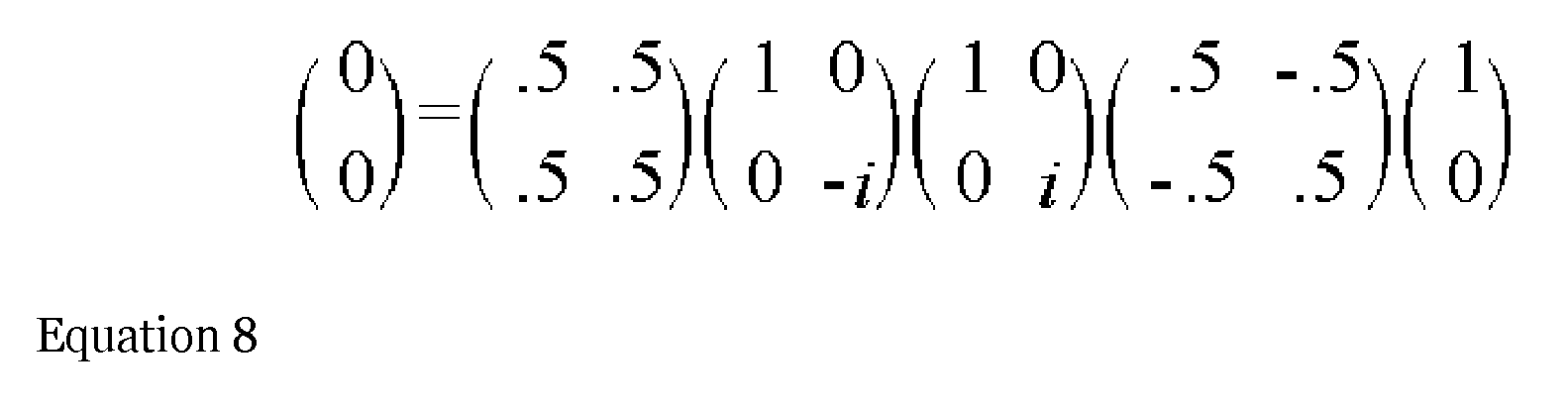
- In conclusion, referring to
FIG. 12 , if thefirst polarizer 21 and thesecond polarizer 22b have different polarizing axes and theconversion retarder 61b is controlled to have a different phase-delayed value from that of thefirst retarder 41, then the transmissivitiy of each of the firstexternal light 51 and the secondexternal light 52 passing trough the display device is zero. In other words, the black mode of the display apparatus may be easily realized by changing the phase-delayed value of theconversion retarder 61. - According to example embodiments, the transmissivity of external light through a display apparatus may be controlled by using optical members, such as a polarizer and a retarder, which may operate with no power or a small amount of power and do not lower the transmissivity of external light, instead of a high-power consuming device, such as a shutter, which greatly lowers the transmissivity of external light. That is, the phase of light and a direction in which the light is polarized may be changed by using a combination of the optical members.
-
FIG. 13 is a schematic cross-sectional view of adisplay apparatus 100" according to another embodiment. Referring toFIG. 13 , thefirst polarizer 21, thefirst retarder 41, thetransparent display device 10, aconverter 65, and thesecond polarizer 22 may be disposed in thedisplay apparatus 100", similar to thedisplay apparatus 100 ofFIG. 1 . Theconverter 65 is a switchable retarder corresponding to theconversion retarder 61 ofFIG. 1 or5 . Theconverter 65 may include asecond retarder 62 and aliquid crystal layer 64. Thesecond retarder 62 may be disposed between thetransparent display device 10 and theliquid crystal layer 64, and theliquid crystal layer 64 may be disposed between thesecond retarder 62 and thesecond polarizer 22. A liquid crystal layer of theliquid crystal layer 64, e.g., that is generally used in a liquid crystal monitor, is inexpensive and is easy to obtain. Theliquid crystal layer 64 may be a switchable retarder that delays incident light by 0 degrees or +1/2 wavelength (+λ/2) or by (-1/2) wavelength (-λ/2) or 0 degrees. Thesecond retarder 62 may delay incident light by +1/4 wavelength (+λ/4) or by (-1/4) wavelength (-λ/4). The other elements illustrated inFIG. 13 correspond to those illustrated inFIG. 1 or5 and thus are not described again here. - The
converter 65 may be a switchable retarder that phase-delays incident light within a range from (-1/4) wavelength (-λ/4) to +1/4 wavelength (+λ/4) by using a combination of theliquid crystal layer 64 and thesecond retarder 62, like theconversion retarder 61 ofFIG.1 or5 . - For example, a case where the
second retarder 62 is a switchable retarder that delays incident light by (-1/4) wavelength (-λ/4) and theliquid crystal layer 64 delays the incident light by 0 degrees or +1/2 wavelength (+λ/2) will be described. In this case, a phase-delayed value of theconverter 65 that is a combination of thesecond retarder 62 and theliquid crystal layer 64 may be (-λ/4) + (0) = (-λ/4) or (-λ/4) + (+λ/2) = (+λ/4). That is, the phase-delayed value of theconverter 65 may be equal to that of theconversion retarder 61 ofFIG. 1 or5 . In other words, theconverter 65 may be used instead of theconversion retarder 61. - As another example, a case where the
second retarder 62 is a switchable retarder that delays incident light by +1/4 wavelength (+λ/4) and theliquid crystal layer 64 delays the incident light by (-1/2) wavelength (-λ/2) or 0 degrees will be described. In this case, a phase-delayed value of theconverter 65 that is a combination of thesecond retarder 62 and theliquid crystal layer 64 may be (+λ/4) + (-λ/2) = (-λ/4) or (+λ/4) + (0) = (+λ/4). In other words, the phase-delayed value of theconverter 65 is equal to that of theconversion retarder 61 ofFIG. 1 or5 . Therefore, theconverter 65 may be used instead of theconversion retarder 61. - According to example embodiments, the
display apparatus 100" that controls the transmissivity of external light therethrough according to a mode may be manufactured by using a simple combination of optical members, such as a retarder and a liquid crystal layer, instead of theconversion retarder 61. In thedisplay apparatus 100" ofFIG. 13 , the transparent mode and the black mode may be realized in a similar manner to the ways described above with reference toFIGS. 9 and10 , according to a voltage applied to theliquid crystal layer 64, and by using a combination of thefirst polarizer 21 and thesecond polarizer 22, when thefirst polarizer 21 and thesecond polarizer 22 have the same polarizing axis. - Although not shown in
FIG. 13 , the embodiments ofFIGS. 9 to 12 may be also performed when thetransparent display device 10 is a top emission type display device like inFIG. 5 or when thetransparent display device 10 is a bottom emission type display device. - In the claims set forth herein, a first phase may be (+λ/4), a second phase may be (-λ/4) or (+λ/4), a third phase may be 0 degrees, a fourth phase may be (+λ/2), a fifth phase may be (-λ/2), and a sixth phase may be 0 degrees. Otherwise, the first phase may be 90 degrees, the second phase may be (-90) degrees or 270 degrees, the third and sixth phases may be 0 degrees or 360 degrees, and the fourth and fifth phases may be 180 degrees. However, the example embodiments are not limited thereto.
- According to the above embodiments, optical members may be disposed in a transparent display device, and the transmissivity of external light through the transparent display device may be controlled according to a mode with a small amount of power.
- Example embodiments have been disclosed herein, and although specific terms are employed, they are used and are to be interpreted in a generic and descriptive sense only and not for purpose of limitation. In some instances, as would be apparent to one of ordinary skill in the art as of the filing of the present application, features, characteristics, and/or elements described in connection with a particular embodiment may be used singly or in combination with features, characteristics, and/or elements described in connection with other embodiments unless otherwise specifically indicated. Accordingly, it will be understood by those of skill in the art that various changes in form and details may be made without departing from the scope of the invention as set forth in the following claims.
Claims (15)
- A display apparatus for controlling optical transmissivity, the display apparatus comprising:a transparent display device, the transparent display device including a pixel divided into a first region for emitting light and a second region adjacent to the first region for transmitting external light therethrough;a first polarizer on a first surface of the transparent display device, the first polarizer being configured to linearly polarize the external light and to transmit the linearly polarized light therethrough;a first retarder between the first polarizer and the first surface of the transparent display device, the first retarder being configured to delay a phase of the external light and to transmit the phase-delayed light therethrough;a second polarizer on a second surface of the transparent display device, the first and second surfaces of the transparent display device being opposite to each other, and the second polarizer being configured to linearly polarize the external light and to transmit the linearly polarized light therethrough; anda conversion retarder between the second polarizer and the second surface of the transparent display device, the conversion retarder being configured to delay a wavelength of the external light within a range from a first phase to a second phase and to transmit the wavelength-delayed light therethrough when power is supplied to the conversion retarder.
- The display apparatus of claim 1, wherein the first polarizer and the second polarizer have the same polarizing axis.
- The display apparatus of claim 1 or 2, wherein the first retarder is configured to delay the wavelength of the external light by the first phase.
- The display apparatus of claim 1, 2 or 3, wherein the conversion retarder is configured to delay the wavelength of the external light by the first phase in accordance with the power supplied thereto, the first and second phases having the same absolute value but different directions, and the display apparatus being configured to block transmittance of external light therethrough, or
wherein the conversion retarder is configured to delay the wavelength of the external light by the second phase in accordance with the power supplied thereto, the first and second phases having the same absolute value but different directions, and the display apparatus being configured to transmit external light therethrough. - The display apparatus of claim 1, wherein the first polarizer and the second polarizer have polarizing axes that are perpendicular to each other.
- The display apparatus of claim 5, wherein the first retarder is configured to delay the wavelength of the external light by the first phase.
- The display apparatus of claim 5 or 6, wherein the conversion retarder is configured to delay the wavelength of the external light by the first phase in accordance with the power supplied thereto, the first and second phases having the same absolute value but different directions, and the display apparatus being configured to transmit external light therethrough, or
wherein the conversion retarder is configured to delay the wavelength of the external light by the second phase in accordance with the power supplied thereto, the first and second phases having the same absolute value but different directions, and the display apparatus being configured to block transmittance of external light therethrough. - The display apparatus of claim 1, wherein the conversion retarder includes a second retarder and a liquid crystal layer, the second retarder being between the transparent display device and the liquid crystal layer, the liquid crystal layer being between the second retarder and the second polarizer, and the liquid crystal layer being configured to delay the wavelength of the external light within the predetermined range in accordance with voltage applied thereto.
- The display apparatus of claim 8, wherein the first polarizer and the second polarizer have the same polarizing axis, the first retarder being configured to delay the wavelength of the external light by the first phase.
- The display apparatus of claim 9, wherein:the second retarder is configured to delay the wavelength of the external light by the second phase,the liquid crystal layer is configured to delay the wavelength of the external light within a range from a third phase to a fourth phase when voltage is applied to the liquid crystal layer, anda sum of the third phase and the fourth phase is equal to the fourth phase, a sum of the fourth phase and the second phase is equal to the first phase, and the first phase and the second phase having the same absolute value but different directions, orwherein:the second retarder is configured to delay the wavelength of the external light by the first phase,the liquid crystal layer is configured to delay the wavelength of the external light within a range from a fifth phase to a sixth phase when voltage is applied to the liquid crystal layer, anda sum of the fifth phase and the first phase is equal to the second phase, a sum of the sixth phase and the first phase is equal to the first phase, and the first phase and the second phase have the same absolute value but different directions.
- The display apparatus of claim 8, wherein the first polarizer and the second polarizer have polarizing axes perpendicular to each other, the first retarder being configured to delay the wavelength of the external light by the first phase.
- The display apparatus of claim 11, wherein:the second retarder is configured to delay the wavelength of the external light by the second phase,the liquid crystal layer is configured to delay the wavelength of the external light within a range from a third phase to a fourth phase when voltage is applied to the liquid crystal layer, anda sum of the third phase and the fourth phase is equal to the fourth phase, the sum of the fourth phase and the second phase is equal to the first phase, and the first phase and the second phase have the same absolute value but different directions, orwherein:the second retarder is configured to delay the wavelength of the external light by the first phase,the liquid crystal layer is configured to delay the wavelength of the external light within a range from a fifth phase to a sixth phase when voltage is applied to the liquid crystal layer, anda sum of the fifth phase and the first phase is equal to the second phase, the sum of the sixth phase and the first phase is equal to the first phase, and the first phase and the second phase have the same absolute value but different directions.
- The display apparatus of any one of the preceding claims, wherein the pixel includes:a pixel circuit unit in the first region and including at least one thin-film transistor (TFT);a first insulating layer covering at least the pixel circuit unit;a first electrode on the first insulating layer to be electrically connected to the pixel circuit unit, the first electrode being located in the first region;a second electrode in at least the first region of the pixel and facing the first electrode; andan organic layer between the first electrode and the second electrode, the organic layer including an emission layer.
- The display apparatus of any one of the preceding claims, wherein the conversion retarder is a switchable retarder having at least two different phase states.
- The display apparatus of claim 1, wherein the first retarder and the conversion retarder include different materials, and/or wherein the conversion retarder includes liquid crystals.
Applications Claiming Priority (1)
| Application Number | Priority Date | Filing Date | Title |
|---|---|---|---|
| KR1020110062489A KR101885698B1 (en) | 2011-06-27 | 2011-06-27 | Display device |
Publications (3)
| Publication Number | Publication Date |
|---|---|
| EP2541317A2 true EP2541317A2 (en) | 2013-01-02 |
| EP2541317A3 EP2541317A3 (en) | 2014-02-26 |
| EP2541317B1 EP2541317B1 (en) | 2016-06-08 |
Family
ID=45812731
Family Applications (1)
| Application Number | Title | Priority Date | Filing Date |
|---|---|---|---|
| EP12159170.5A Active EP2541317B1 (en) | 2011-06-27 | 2012-03-13 | Display apparatus for controlling optical transmissivity |
Country Status (6)
| Country | Link |
|---|---|
| US (2) | US9128338B2 (en) |
| EP (1) | EP2541317B1 (en) |
| JP (1) | JP6054066B2 (en) |
| KR (1) | KR101885698B1 (en) |
| CN (2) | CN102856347B (en) |
| TW (1) | TWI554807B (en) |
Cited By (5)
| Publication number | Priority date | Publication date | Assignee | Title |
|---|---|---|---|---|
| WO2015119453A1 (en) | 2014-02-07 | 2015-08-13 | Samsung Electronics Co., Ltd. | Dual-mode display |
| US10375365B2 (en) | 2014-02-07 | 2019-08-06 | Samsung Electronics Co., Ltd. | Projection system with enhanced color and contrast |
| US10453371B2 (en) | 2014-02-07 | 2019-10-22 | Samsung Electronics Co., Ltd. | Multi-layer display with color and contrast enhancement |
| US10554962B2 (en) | 2014-02-07 | 2020-02-04 | Samsung Electronics Co., Ltd. | Multi-layer high transparency display for light field generation |
| US10565925B2 (en) | 2014-02-07 | 2020-02-18 | Samsung Electronics Co., Ltd. | Full color display with intrinsic transparency |
Families Citing this family (34)
| Publication number | Priority date | Publication date | Assignee | Title |
|---|---|---|---|---|
| KR101885698B1 (en) * | 2011-06-27 | 2018-08-07 | 삼성디스플레이 주식회사 | Display device |
| KR102080007B1 (en) | 2012-05-25 | 2020-02-24 | 삼성디스플레이 주식회사 | Display device |
| KR101338250B1 (en) | 2012-06-07 | 2013-12-09 | 삼성디스플레이 주식회사 | Display device |
| CN103576357B (en) * | 2012-07-24 | 2016-12-21 | 上海天马微电子有限公司 | Transparent display |
| KR101982073B1 (en) * | 2012-10-12 | 2019-05-27 | 삼성디스플레이 주식회사 | Organic light emitting diode and organic light emitting diode display |
| KR102037273B1 (en) * | 2012-12-28 | 2019-11-27 | 삼성디스플레이 주식회사 | Organic light emitting device |
| US9594286B2 (en) * | 2012-12-31 | 2017-03-14 | Lg Display Co., Ltd. | Transparent display apparatus with adjustable transmissive area and a method for controlling the same |
| US9240162B2 (en) * | 2012-12-31 | 2016-01-19 | Lg Display Co., Ltd. | Transparent display apparatus and method for controlling the same |
| WO2014104858A1 (en) * | 2012-12-31 | 2014-07-03 | 엘지디스플레이 주식회사 | Transparent display device and method for controlling same |
| CN103913889B (en) * | 2012-12-31 | 2017-05-24 | 上海天马微电子有限公司 | Liquid crystal display device with built-in light source |
| CN104008730A (en) * | 2013-02-26 | 2014-08-27 | 联想(北京)有限公司 | Display apparatus and electronic device |
| KR101503908B1 (en) * | 2013-02-26 | 2015-03-19 | 한성희 | Light modulating unit and stereoscopic display apparatus comprising the same |
| US9812075B2 (en) | 2013-02-26 | 2017-11-07 | Beijing Lenovo Software Ltd. | Display screen, electronic device and information processing method for the electronic device |
| KR102223674B1 (en) * | 2013-11-28 | 2021-03-08 | 삼성디스플레이 주식회사 | Organic light emitting display device |
| KR102283456B1 (en) | 2013-12-18 | 2021-07-30 | 삼성디스플레이 주식회사 | Display device |
| CN103811532B (en) * | 2014-01-28 | 2016-07-06 | 京东方科技集团股份有限公司 | A kind of display device and preparation method thereof |
| CN105336759B (en) * | 2014-08-06 | 2018-06-29 | 上海和辉光电有限公司 | Display panel |
| KR20160053001A (en) * | 2014-10-30 | 2016-05-13 | 삼성디스플레이 주식회사 | Transparent display substrates, transparent display devices and methods of manufacturing transparent display devices |
| KR102335214B1 (en) * | 2014-11-18 | 2021-12-06 | 삼성디스플레이 주식회사 | Display panel |
| KR102338907B1 (en) * | 2015-02-13 | 2021-12-14 | 삼성디스플레이 주식회사 | Liquid crystal display apparatus and method for manufacturing the same |
| EP3086170B1 (en) * | 2015-04-21 | 2020-12-02 | LG Display Co., Ltd. | Liquid crystal display |
| KR102453566B1 (en) * | 2015-06-01 | 2022-10-13 | 삼성디스플레이 주식회사 | Display device and manufacturing method thereof |
| KR102405312B1 (en) * | 2015-10-06 | 2022-06-02 | 엘지디스플레이 주식회사 | Light controlling device, transparent display device including the same, and method for fabricating the same |
| KR102471111B1 (en) * | 2015-11-23 | 2022-11-28 | 삼성디스플레이 주식회사 | Organic light-emitting display apparatus and method for manufacturing the same |
| KR102598924B1 (en) * | 2015-12-15 | 2023-11-03 | 엘지디스플레이 주식회사 | Organic light emitting diodes display panel |
| KR102472607B1 (en) * | 2016-02-03 | 2022-11-30 | 삼성디스플레이 주식회사 | Display device |
| KR102574641B1 (en) * | 2016-07-19 | 2023-09-06 | 삼성디스플레이 주식회사 | Display appartus |
| KR102670056B1 (en) * | 2016-11-18 | 2024-05-30 | 삼성디스플레이 주식회사 | Display apparatus and method of manufacturing the same |
| US11500255B2 (en) * | 2018-11-07 | 2022-11-15 | Alphamicron Incorporated | Variable transmission optical assembly having a pixelated switchable birefringent layer |
| TWI683144B (en) * | 2018-12-22 | 2020-01-21 | 友達光電股份有限公司 | Polarizer module and operation method thereof |
| US20220352481A1 (en) * | 2019-10-08 | 2022-11-03 | Sharp Kabushiki Kaisha | Light-emitting device |
| CN110989191B (en) * | 2019-12-20 | 2022-03-04 | 京东方科技集团股份有限公司 | Integrated display panel, method for making the same, and display device |
| KR102776381B1 (en) | 2020-04-02 | 2025-03-10 | 삼성디스플레이 주식회사 | Display apparatus and Method of manufacturing of the same |
| JP2023147063A (en) * | 2022-03-29 | 2023-10-12 | パナソニックIpマネジメント株式会社 | display device |
Family Cites Families (23)
| Publication number | Priority date | Publication date | Assignee | Title |
|---|---|---|---|---|
| US5187603A (en) | 1990-06-26 | 1993-02-16 | Tektronix, Inc. | High contrast light shutter system |
| US6727967B2 (en) | 1998-10-15 | 2004-04-27 | Kabushiki Kaisha Toshiba | Transelective lcd in which reflected light passes through color filters twice, transmitted light passes through color filter only once, but also passes through additional layer of cholesteric liquid crystal or band-pass filter |
| JP2000131684A (en) * | 1998-10-22 | 2000-05-12 | Toshiba Corp | Liquid crystal display device |
| JP3767419B2 (en) * | 2001-05-28 | 2006-04-19 | ソニー株式会社 | Liquid crystal display element |
| KR20050057655A (en) | 2002-10-16 | 2005-06-16 | 코닌클리케 필립스 일렉트로닉스 엔.브이. | Drift-free video encoding and decoding method, and corresponding devices |
| KR101061396B1 (en) * | 2003-02-28 | 2011-09-02 | 가부시키가이샤 한도오따이 에네루기 켄큐쇼 | Display device, clamshell terminal |
| JP2005250501A (en) * | 2003-02-28 | 2005-09-15 | Semiconductor Energy Lab Co Ltd | Display device and folding portable terminal |
| JP4131838B2 (en) * | 2003-05-16 | 2008-08-13 | 株式会社半導体エネルギー研究所 | Display device |
| JP4552415B2 (en) | 2003-10-14 | 2010-09-29 | 信越半導体株式会社 | Method for manufacturing silicon wafer |
| JP4287337B2 (en) * | 2003-11-24 | 2009-07-01 | 三星モバイルディスプレイ株式會社 | Organic electroluminescent display device and manufacturing method thereof |
| JP4668549B2 (en) * | 2004-04-21 | 2011-04-13 | 大日本印刷株式会社 | Optical compensation element with variable phase difference and liquid crystal display using the same |
| KR20050113045A (en) * | 2004-05-28 | 2005-12-01 | 삼성에스디아이 주식회사 | Organic light emitting display device and the method for fabricating of the same |
| TWI284768B (en) * | 2004-07-02 | 2007-08-01 | Innolux Display Corp | Transflective liquid crystal display device |
| JP4752240B2 (en) * | 2004-10-27 | 2011-08-17 | セイコーエプソン株式会社 | Display device and electronic device |
| KR100719706B1 (en) | 2005-09-13 | 2007-05-17 | 삼성에스디아이 주식회사 | Flat panel display and organic light emitting display |
| KR101398330B1 (en) * | 2007-08-31 | 2014-05-26 | 엘지디스플레이 주식회사 | Transreflective liquid crystal display and method for manufacturing the same |
| US20090147185A1 (en) | 2007-12-05 | 2009-06-11 | Emiscape, Inc. | Reflective One-Way Screen with Chromatic and Transparent Regions |
| KR100995067B1 (en) | 2009-01-21 | 2010-11-18 | 삼성모바일디스플레이주식회사 | Organic light emitting display |
| KR20100137695A (en) | 2009-06-23 | 2010-12-31 | 주식회사 링크텍스 | Stereoscopic image realization system with liquid crystal shutter and glasses filter |
| KR101641713B1 (en) | 2009-08-13 | 2016-07-22 | 삼성디스플레이 주식회사 | Organic light emitting diode display |
| KR101084240B1 (en) | 2009-12-21 | 2011-11-16 | 삼성모바일디스플레이주식회사 | Organic light emitting diode display |
| KR101407586B1 (en) * | 2011-04-25 | 2014-06-27 | 삼성디스플레이 주식회사 | Display device and operating method thereof |
| KR101885698B1 (en) * | 2011-06-27 | 2018-08-07 | 삼성디스플레이 주식회사 | Display device |
-
2011
- 2011-06-27 KR KR1020110062489A patent/KR101885698B1/en active Active
-
2012
- 2012-02-21 US US13/401,059 patent/US9128338B2/en active Active
- 2012-02-24 TW TW101106141A patent/TWI554807B/en active
- 2012-03-13 EP EP12159170.5A patent/EP2541317B1/en active Active
- 2012-05-25 CN CN201210167194.5A patent/CN102856347B/en active Active
- 2012-05-25 CN CN2012202414116U patent/CN202712191U/en not_active Expired - Lifetime
- 2012-06-12 JP JP2012133266A patent/JP6054066B2/en active Active
-
2015
- 2015-09-03 US US14/844,452 patent/US9448437B2/en active Active
Non-Patent Citations (1)
| Title |
|---|
| None |
Cited By (7)
| Publication number | Priority date | Publication date | Assignee | Title |
|---|---|---|---|---|
| WO2015119453A1 (en) | 2014-02-07 | 2015-08-13 | Samsung Electronics Co., Ltd. | Dual-mode display |
| US10375365B2 (en) | 2014-02-07 | 2019-08-06 | Samsung Electronics Co., Ltd. | Projection system with enhanced color and contrast |
| US10380933B2 (en) | 2014-02-07 | 2019-08-13 | Samsung Electronics Company, Ltd. | Display with high transparency |
| US10453371B2 (en) | 2014-02-07 | 2019-10-22 | Samsung Electronics Co., Ltd. | Multi-layer display with color and contrast enhancement |
| US10554962B2 (en) | 2014-02-07 | 2020-02-04 | Samsung Electronics Co., Ltd. | Multi-layer high transparency display for light field generation |
| US10565925B2 (en) | 2014-02-07 | 2020-02-18 | Samsung Electronics Co., Ltd. | Full color display with intrinsic transparency |
| EP3103110B1 (en) * | 2014-02-07 | 2020-10-28 | Samsung Electronics Co., Ltd. | Dual-mode display |
Also Published As
| Publication number | Publication date |
|---|---|
| TW201300889A (en) | 2013-01-01 |
| US9448437B2 (en) | 2016-09-20 |
| US20150378201A1 (en) | 2015-12-31 |
| US20120327331A1 (en) | 2012-12-27 |
| CN102856347B (en) | 2017-11-21 |
| KR20130006947A (en) | 2013-01-18 |
| JP2013012734A (en) | 2013-01-17 |
| US9128338B2 (en) | 2015-09-08 |
| EP2541317B1 (en) | 2016-06-08 |
| EP2541317A3 (en) | 2014-02-26 |
| JP6054066B2 (en) | 2016-12-27 |
| KR101885698B1 (en) | 2018-08-07 |
| TWI554807B (en) | 2016-10-21 |
| CN102856347A (en) | 2013-01-02 |
| CN202712191U (en) | 2013-01-30 |
Similar Documents
| Publication | Publication Date | Title |
|---|---|---|
| EP2541317B1 (en) | Display apparatus for controlling optical transmissivity | |
| KR101407586B1 (en) | Display device and operating method thereof | |
| US9391127B2 (en) | Display device for controlling light transmittance | |
| US9709844B2 (en) | Display apparatus capable of controlling light transmittance and method of manufacturing the same | |
| KR101338250B1 (en) | Display device | |
| KR100995067B1 (en) | Organic light emitting display | |
| EP2618379B1 (en) | Organic light emitting display device | |
| US8736790B2 (en) | Organic light emitting diode display with liquid crystal layer | |
| US20130328945A1 (en) | Display device and method of operating the same | |
| US20120320287A1 (en) | Display device |
Legal Events
| Date | Code | Title | Description |
|---|---|---|---|
| PUAI | Public reference made under article 153(3) epc to a published international application that has entered the european phase |
Free format text: ORIGINAL CODE: 0009012 |
|
| AK | Designated contracting states |
Kind code of ref document: A2 Designated state(s): AL AT BE BG CH CY CZ DE DK EE ES FI FR GB GR HR HU IE IS IT LI LT LU LV MC MK MT NL NO PL PT RO RS SE SI SK SM TR |
|
| AX | Request for extension of the european patent |
Extension state: BA ME |
|
| PUAL | Search report despatched |
Free format text: ORIGINAL CODE: 0009013 |
|
| AK | Designated contracting states |
Kind code of ref document: A3 Designated state(s): AL AT BE BG CH CY CZ DE DK EE ES FI FR GB GR HR HU IE IS IT LI LT LU LV MC MK MT NL NO PL PT RO RS SE SI SK SM TR |
|
| AX | Request for extension of the european patent |
Extension state: BA ME |
|
| RIC1 | Information provided on ipc code assigned before grant |
Ipc: G02F 1/1362 20060101AFI20140122BHEP Ipc: H01L 51/00 20060101ALI20140122BHEP |
|
| 17P | Request for examination filed |
Effective date: 20140331 |
|
| RBV | Designated contracting states (corrected) |
Designated state(s): AL AT BE BG CH CY CZ DE DK EE ES FI FR GB GR HR HU IE IS IT LI LT LU LV MC MK MT NL NO PL PT RO RS SE SI SK SM TR |
|
| 17Q | First examination report despatched |
Effective date: 20150417 |
|
| RAP1 | Party data changed (applicant data changed or rights of an application transferred) |
Owner name: SAMSUNG DISPLAY CO., LTD. |
|
| GRAP | Despatch of communication of intention to grant a patent |
Free format text: ORIGINAL CODE: EPIDOSNIGR1 |
|
| INTG | Intention to grant announced |
Effective date: 20160127 |
|
| GRAS | Grant fee paid |
Free format text: ORIGINAL CODE: EPIDOSNIGR3 |
|
| GRAA | (expected) grant |
Free format text: ORIGINAL CODE: 0009210 |
|
| AK | Designated contracting states |
Kind code of ref document: B1 Designated state(s): AL AT BE BG CH CY CZ DE DK EE ES FI FR GB GR HR HU IE IS IT LI LT LU LV MC MK MT NL NO PL PT RO RS SE SI SK SM TR |
|
| REG | Reference to a national code |
Ref country code: GB Ref legal event code: FG4D |
|
| REG | Reference to a national code |
Ref country code: CH Ref legal event code: EP |
|
| REG | Reference to a national code |
Ref country code: IE Ref legal event code: FG4D |
|
| REG | Reference to a national code |
Ref country code: AT Ref legal event code: REF Ref document number: 805648 Country of ref document: AT Kind code of ref document: T Effective date: 20160715 |
|
| REG | Reference to a national code |
Ref country code: DE Ref legal event code: R096 Ref document number: 602012019312 Country of ref document: DE |
|
| REG | Reference to a national code |
Ref country code: LT Ref legal event code: MG4D |
|
| REG | Reference to a national code |
Ref country code: NL Ref legal event code: MP Effective date: 20160608 |
|
| PG25 | Lapsed in a contracting state [announced via postgrant information from national office to epo] |
Ref country code: FI Free format text: LAPSE BECAUSE OF FAILURE TO SUBMIT A TRANSLATION OF THE DESCRIPTION OR TO PAY THE FEE WITHIN THE PRESCRIBED TIME-LIMIT Effective date: 20160608 Ref country code: NO Free format text: LAPSE BECAUSE OF FAILURE TO SUBMIT A TRANSLATION OF THE DESCRIPTION OR TO PAY THE FEE WITHIN THE PRESCRIBED TIME-LIMIT Effective date: 20160908 Ref country code: LT Free format text: LAPSE BECAUSE OF FAILURE TO SUBMIT A TRANSLATION OF THE DESCRIPTION OR TO PAY THE FEE WITHIN THE PRESCRIBED TIME-LIMIT Effective date: 20160608 |
|
| REG | Reference to a national code |
Ref country code: AT Ref legal event code: MK05 Ref document number: 805648 Country of ref document: AT Kind code of ref document: T Effective date: 20160608 |
|
| PG25 | Lapsed in a contracting state [announced via postgrant information from national office to epo] |
Ref country code: LV Free format text: LAPSE BECAUSE OF FAILURE TO SUBMIT A TRANSLATION OF THE DESCRIPTION OR TO PAY THE FEE WITHIN THE PRESCRIBED TIME-LIMIT Effective date: 20160608 Ref country code: SE Free format text: LAPSE BECAUSE OF FAILURE TO SUBMIT A TRANSLATION OF THE DESCRIPTION OR TO PAY THE FEE WITHIN THE PRESCRIBED TIME-LIMIT Effective date: 20160608 Ref country code: ES Free format text: LAPSE BECAUSE OF FAILURE TO SUBMIT A TRANSLATION OF THE DESCRIPTION OR TO PAY THE FEE WITHIN THE PRESCRIBED TIME-LIMIT Effective date: 20160608 Ref country code: RS Free format text: LAPSE BECAUSE OF FAILURE TO SUBMIT A TRANSLATION OF THE DESCRIPTION OR TO PAY THE FEE WITHIN THE PRESCRIBED TIME-LIMIT Effective date: 20160608 Ref country code: HR Free format text: LAPSE BECAUSE OF FAILURE TO SUBMIT A TRANSLATION OF THE DESCRIPTION OR TO PAY THE FEE WITHIN THE PRESCRIBED TIME-LIMIT Effective date: 20160608 Ref country code: NL Free format text: LAPSE BECAUSE OF FAILURE TO SUBMIT A TRANSLATION OF THE DESCRIPTION OR TO PAY THE FEE WITHIN THE PRESCRIBED TIME-LIMIT Effective date: 20160608 Ref country code: GR Free format text: LAPSE BECAUSE OF FAILURE TO SUBMIT A TRANSLATION OF THE DESCRIPTION OR TO PAY THE FEE WITHIN THE PRESCRIBED TIME-LIMIT Effective date: 20160909 |
|
| PG25 | Lapsed in a contracting state [announced via postgrant information from national office to epo] |
Ref country code: EE Free format text: LAPSE BECAUSE OF FAILURE TO SUBMIT A TRANSLATION OF THE DESCRIPTION OR TO PAY THE FEE WITHIN THE PRESCRIBED TIME-LIMIT Effective date: 20160608 Ref country code: SK Free format text: LAPSE BECAUSE OF FAILURE TO SUBMIT A TRANSLATION OF THE DESCRIPTION OR TO PAY THE FEE WITHIN THE PRESCRIBED TIME-LIMIT Effective date: 20160608 Ref country code: RO Free format text: LAPSE BECAUSE OF FAILURE TO SUBMIT A TRANSLATION OF THE DESCRIPTION OR TO PAY THE FEE WITHIN THE PRESCRIBED TIME-LIMIT Effective date: 20160608 Ref country code: IS Free format text: LAPSE BECAUSE OF FAILURE TO SUBMIT A TRANSLATION OF THE DESCRIPTION OR TO PAY THE FEE WITHIN THE PRESCRIBED TIME-LIMIT Effective date: 20161008 Ref country code: CZ Free format text: LAPSE BECAUSE OF FAILURE TO SUBMIT A TRANSLATION OF THE DESCRIPTION OR TO PAY THE FEE WITHIN THE PRESCRIBED TIME-LIMIT Effective date: 20160608 Ref country code: IT Free format text: LAPSE BECAUSE OF FAILURE TO SUBMIT A TRANSLATION OF THE DESCRIPTION OR TO PAY THE FEE WITHIN THE PRESCRIBED TIME-LIMIT Effective date: 20160608 |
|
| REG | Reference to a national code |
Ref country code: FR Ref legal event code: PLFP Year of fee payment: 6 |
|
| PG25 | Lapsed in a contracting state [announced via postgrant information from national office to epo] |
Ref country code: SM Free format text: LAPSE BECAUSE OF FAILURE TO SUBMIT A TRANSLATION OF THE DESCRIPTION OR TO PAY THE FEE WITHIN THE PRESCRIBED TIME-LIMIT Effective date: 20160608 Ref country code: AT Free format text: LAPSE BECAUSE OF FAILURE TO SUBMIT A TRANSLATION OF THE DESCRIPTION OR TO PAY THE FEE WITHIN THE PRESCRIBED TIME-LIMIT Effective date: 20160608 Ref country code: PT Free format text: LAPSE BECAUSE OF FAILURE TO SUBMIT A TRANSLATION OF THE DESCRIPTION OR TO PAY THE FEE WITHIN THE PRESCRIBED TIME-LIMIT Effective date: 20161010 Ref country code: PL Free format text: LAPSE BECAUSE OF FAILURE TO SUBMIT A TRANSLATION OF THE DESCRIPTION OR TO PAY THE FEE WITHIN THE PRESCRIBED TIME-LIMIT Effective date: 20160608 Ref country code: BE Free format text: LAPSE BECAUSE OF FAILURE TO SUBMIT A TRANSLATION OF THE DESCRIPTION OR TO PAY THE FEE WITHIN THE PRESCRIBED TIME-LIMIT Effective date: 20160608 |
|
| REG | Reference to a national code |
Ref country code: DE Ref legal event code: R097 Ref document number: 602012019312 Country of ref document: DE |
|
| PLBE | No opposition filed within time limit |
Free format text: ORIGINAL CODE: 0009261 |
|
| STAA | Information on the status of an ep patent application or granted ep patent |
Free format text: STATUS: NO OPPOSITION FILED WITHIN TIME LIMIT |
|
| 26N | No opposition filed |
Effective date: 20170309 |
|
| PG25 | Lapsed in a contracting state [announced via postgrant information from national office to epo] |
Ref country code: SI Free format text: LAPSE BECAUSE OF FAILURE TO SUBMIT A TRANSLATION OF THE DESCRIPTION OR TO PAY THE FEE WITHIN THE PRESCRIBED TIME-LIMIT Effective date: 20160608 Ref country code: DK Free format text: LAPSE BECAUSE OF FAILURE TO SUBMIT A TRANSLATION OF THE DESCRIPTION OR TO PAY THE FEE WITHIN THE PRESCRIBED TIME-LIMIT Effective date: 20160608 |
|
| REG | Reference to a national code |
Ref country code: CH Ref legal event code: PL |
|
| PG25 | Lapsed in a contracting state [announced via postgrant information from national office to epo] |
Ref country code: MC Free format text: LAPSE BECAUSE OF FAILURE TO SUBMIT A TRANSLATION OF THE DESCRIPTION OR TO PAY THE FEE WITHIN THE PRESCRIBED TIME-LIMIT Effective date: 20160608 |
|
| REG | Reference to a national code |
Ref country code: IE Ref legal event code: MM4A |
|
| PG25 | Lapsed in a contracting state [announced via postgrant information from national office to epo] |
Ref country code: LU Free format text: LAPSE BECAUSE OF NON-PAYMENT OF DUE FEES Effective date: 20170313 |
|
| REG | Reference to a national code |
Ref country code: FR Ref legal event code: PLFP Year of fee payment: 7 |
|
| PG25 | Lapsed in a contracting state [announced via postgrant information from national office to epo] |
Ref country code: CH Free format text: LAPSE BECAUSE OF NON-PAYMENT OF DUE FEES Effective date: 20170331 Ref country code: IE Free format text: LAPSE BECAUSE OF NON-PAYMENT OF DUE FEES Effective date: 20170313 Ref country code: LI Free format text: LAPSE BECAUSE OF NON-PAYMENT OF DUE FEES Effective date: 20170331 |
|
| PG25 | Lapsed in a contracting state [announced via postgrant information from national office to epo] |
Ref country code: MT Free format text: LAPSE BECAUSE OF NON-PAYMENT OF DUE FEES Effective date: 20170313 |
|
| PG25 | Lapsed in a contracting state [announced via postgrant information from national office to epo] |
Ref country code: AL Free format text: LAPSE BECAUSE OF FAILURE TO SUBMIT A TRANSLATION OF THE DESCRIPTION OR TO PAY THE FEE WITHIN THE PRESCRIBED TIME-LIMIT Effective date: 20160608 |
|
| PG25 | Lapsed in a contracting state [announced via postgrant information from national office to epo] |
Ref country code: HU Free format text: LAPSE BECAUSE OF FAILURE TO SUBMIT A TRANSLATION OF THE DESCRIPTION OR TO PAY THE FEE WITHIN THE PRESCRIBED TIME-LIMIT; INVALID AB INITIO Effective date: 20120313 |
|
| PG25 | Lapsed in a contracting state [announced via postgrant information from national office to epo] |
Ref country code: BG Free format text: LAPSE BECAUSE OF FAILURE TO SUBMIT A TRANSLATION OF THE DESCRIPTION OR TO PAY THE FEE WITHIN THE PRESCRIBED TIME-LIMIT Effective date: 20160608 |
|
| PG25 | Lapsed in a contracting state [announced via postgrant information from national office to epo] |
Ref country code: CY Free format text: LAPSE BECAUSE OF NON-PAYMENT OF DUE FEES Effective date: 20160608 |
|
| PG25 | Lapsed in a contracting state [announced via postgrant information from national office to epo] |
Ref country code: MK Free format text: LAPSE BECAUSE OF FAILURE TO SUBMIT A TRANSLATION OF THE DESCRIPTION OR TO PAY THE FEE WITHIN THE PRESCRIBED TIME-LIMIT Effective date: 20160608 |
|
| PG25 | Lapsed in a contracting state [announced via postgrant information from national office to epo] |
Ref country code: TR Free format text: LAPSE BECAUSE OF FAILURE TO SUBMIT A TRANSLATION OF THE DESCRIPTION OR TO PAY THE FEE WITHIN THE PRESCRIBED TIME-LIMIT Effective date: 20160608 |
|
| P01 | Opt-out of the competence of the unified patent court (upc) registered |
Effective date: 20230515 |
|
| PGFP | Annual fee paid to national office [announced via postgrant information from national office to epo] |
Ref country code: GB Payment date: 20260224 Year of fee payment: 15 |
|
| PGFP | Annual fee paid to national office [announced via postgrant information from national office to epo] |
Ref country code: DE Payment date: 20260220 Year of fee payment: 15 |
|
| PGFP | Annual fee paid to national office [announced via postgrant information from national office to epo] |
Ref country code: FR Payment date: 20260224 Year of fee payment: 15 |