EP2540733A1 - Deposition of indium containing thin films using new indium precursors - Google Patents
Deposition of indium containing thin films using new indium precursors Download PDFInfo
- Publication number
- EP2540733A1 EP2540733A1 EP11305846A EP11305846A EP2540733A1 EP 2540733 A1 EP2540733 A1 EP 2540733A1 EP 11305846 A EP11305846 A EP 11305846A EP 11305846 A EP11305846 A EP 11305846A EP 2540733 A1 EP2540733 A1 EP 2540733A1
- Authority
- EP
- European Patent Office
- Prior art keywords
- indium
- substrate
- group
- alkylsilyl
- aryl
- Prior art date
- Legal status (The legal status is an assumption and is not a legal conclusion. Google has not performed a legal analysis and makes no representation as to the accuracy of the status listed.)
- Withdrawn
Links
- 229910052738 indium Inorganic materials 0.000 title claims abstract description 40
- APFVFJFRJDLVQX-UHFFFAOYSA-N indium atom Chemical group [In] APFVFJFRJDLVQX-UHFFFAOYSA-N 0.000 title claims abstract description 38
- 239000002243 precursor Substances 0.000 title claims abstract description 33
- 239000010409 thin film Substances 0.000 title claims abstract description 15
- 230000008021 deposition Effects 0.000 title description 14
- 238000000034 method Methods 0.000 claims abstract description 24
- 150000001875 compounds Chemical class 0.000 claims abstract description 22
- 239000000758 substrate Substances 0.000 claims abstract description 21
- 238000000231 atomic layer deposition Methods 0.000 claims abstract description 13
- 125000000217 alkyl group Chemical group 0.000 claims abstract description 12
- 125000005103 alkyl silyl group Chemical group 0.000 claims abstract description 10
- 125000003118 aryl group Chemical group 0.000 claims abstract description 10
- 239000000376 reactant Substances 0.000 claims description 23
- 229910052751 metal Inorganic materials 0.000 claims description 21
- 239000002184 metal Substances 0.000 claims description 21
- 238000006243 chemical reaction Methods 0.000 claims description 12
- 239000012782 phase change material Substances 0.000 claims description 9
- 125000004213 tert-butoxy group Chemical group [H]C([H])([H])C(O*)(C([H])([H])[H])C([H])([H])[H] 0.000 claims description 8
- 238000004519 manufacturing process Methods 0.000 claims description 7
- 125000001495 ethyl group Chemical group [H]C([H])([H])C([H])([H])* 0.000 claims description 4
- 125000002496 methyl group Chemical group [H]C([H])([H])* 0.000 claims description 4
- 239000004065 semiconductor Substances 0.000 claims description 4
- 125000003253 isopropoxy group Chemical group [H]C([H])([H])C([H])(O*)C([H])([H])[H] 0.000 claims description 3
- 239000003153 chemical reaction reagent Substances 0.000 claims description 2
- 125000001449 isopropyl group Chemical group [H]C([H])([H])C([H])(*)C([H])([H])[H] 0.000 claims description 2
- 238000005121 nitriding Methods 0.000 claims description 2
- 230000001590 oxidative effect Effects 0.000 claims description 2
- 125000000999 tert-butyl group Chemical group [H]C([H])([H])C(*)(C([H])([H])[H])C([H])([H])[H] 0.000 claims description 2
- 238000000151 deposition Methods 0.000 description 14
- 239000000203 mixture Substances 0.000 description 12
- 241000894007 species Species 0.000 description 12
- 239000007789 gas Substances 0.000 description 11
- 239000010408 film Substances 0.000 description 10
- IJGRMHOSHXDMSA-UHFFFAOYSA-N Atomic nitrogen Chemical compound N#N IJGRMHOSHXDMSA-UHFFFAOYSA-N 0.000 description 7
- 239000001301 oxygen Substances 0.000 description 7
- 229910052760 oxygen Inorganic materials 0.000 description 7
- QVGXLLKOCUKJST-UHFFFAOYSA-N atomic oxygen Chemical compound [O] QVGXLLKOCUKJST-UHFFFAOYSA-N 0.000 description 6
- 238000009826 distribution Methods 0.000 description 6
- VLKZOEOYAKHREP-UHFFFAOYSA-N n-Hexane Chemical compound CCCCCC VLKZOEOYAKHREP-UHFFFAOYSA-N 0.000 description 6
- 239000002904 solvent Substances 0.000 description 6
- KTSFMFGEAAANTF-UHFFFAOYSA-N [Cu].[Se].[Se].[In] Chemical compound [Cu].[Se].[Se].[In] KTSFMFGEAAANTF-UHFFFAOYSA-N 0.000 description 5
- 238000005229 chemical vapour deposition Methods 0.000 description 5
- 239000007788 liquid Substances 0.000 description 5
- 239000011669 selenium Substances 0.000 description 5
- 230000008016 vaporization Effects 0.000 description 5
- OAKJQQAXSVQMHS-UHFFFAOYSA-N Hydrazine Chemical compound NN OAKJQQAXSVQMHS-UHFFFAOYSA-N 0.000 description 4
- OFBQJSOFQDEBGM-UHFFFAOYSA-N Pentane Chemical compound CCCCC OFBQJSOFQDEBGM-UHFFFAOYSA-N 0.000 description 4
- 239000012159 carrier gas Substances 0.000 description 4
- PJXISJQVUVHSOJ-UHFFFAOYSA-N indium(III) oxide Inorganic materials [O-2].[O-2].[O-2].[In+3].[In+3] PJXISJQVUVHSOJ-UHFFFAOYSA-N 0.000 description 4
- PSCMQHVBLHHWTO-UHFFFAOYSA-K indium(iii) chloride Chemical compound Cl[In](Cl)Cl PSCMQHVBLHHWTO-UHFFFAOYSA-K 0.000 description 4
- 239000012071 phase Substances 0.000 description 4
- 238000010926 purge Methods 0.000 description 4
- IBEFSUTVZWZJEL-UHFFFAOYSA-N trimethylindium Chemical compound C[In](C)C IBEFSUTVZWZJEL-UHFFFAOYSA-N 0.000 description 4
- QGZKDVFQNNGYKY-UHFFFAOYSA-N Ammonia Chemical compound N QGZKDVFQNNGYKY-UHFFFAOYSA-N 0.000 description 3
- RTZKZFJDLAIYFH-UHFFFAOYSA-N Diethyl ether Chemical compound CCOCC RTZKZFJDLAIYFH-UHFFFAOYSA-N 0.000 description 3
- VYPSYNLAJGMNEJ-UHFFFAOYSA-N Silicium dioxide Chemical compound O=[Si]=O VYPSYNLAJGMNEJ-UHFFFAOYSA-N 0.000 description 3
- 229910052786 argon Inorganic materials 0.000 description 3
- 239000003517 fume Substances 0.000 description 3
- -1 indium metal-organic compounds Chemical class 0.000 description 3
- 229910003437 indium oxide Inorganic materials 0.000 description 3
- 230000008018 melting Effects 0.000 description 3
- 238000002844 melting Methods 0.000 description 3
- 229910052757 nitrogen Inorganic materials 0.000 description 3
- 239000000843 powder Substances 0.000 description 3
- 239000012808 vapor phase Substances 0.000 description 3
- 238000009834 vaporization Methods 0.000 description 3
- XKRFYHLGVUSROY-UHFFFAOYSA-N Argon Chemical compound [Ar] XKRFYHLGVUSROY-UHFFFAOYSA-N 0.000 description 2
- 229910006111 GeCl2 Inorganic materials 0.000 description 2
- CBENFWSGALASAD-UHFFFAOYSA-N Ozone Chemical compound [O-][O+]=O CBENFWSGALASAD-UHFFFAOYSA-N 0.000 description 2
- DKGAVHZHDRPRBM-UHFFFAOYSA-N Tert-Butanol Chemical compound CC(C)(C)O DKGAVHZHDRPRBM-UHFFFAOYSA-N 0.000 description 2
- 150000001412 amines Chemical class 0.000 description 2
- FAPDDOBMIUGHIN-UHFFFAOYSA-K antimony trichloride Chemical compound Cl[Sb](Cl)Cl FAPDDOBMIUGHIN-UHFFFAOYSA-K 0.000 description 2
- 239000003849 aromatic solvent Substances 0.000 description 2
- QHGIKMVOLGCZIP-UHFFFAOYSA-N germanium dichloride Chemical compound Cl[Ge]Cl QHGIKMVOLGCZIP-UHFFFAOYSA-N 0.000 description 2
- 239000000463 material Substances 0.000 description 2
- TVMXDCGIABBOFY-UHFFFAOYSA-N octane Chemical compound CCCCCCCC TVMXDCGIABBOFY-UHFFFAOYSA-N 0.000 description 2
- 230000005693 optoelectronics Effects 0.000 description 2
- 150000002902 organometallic compounds Chemical class 0.000 description 2
- 239000002245 particle Substances 0.000 description 2
- 239000003381 stabilizer Substances 0.000 description 2
- 238000000859 sublimation Methods 0.000 description 2
- 230000008022 sublimation Effects 0.000 description 2
- SWLJJEFSPJCUBD-UHFFFAOYSA-N tellurium tetrachloride Chemical compound Cl[Te](Cl)(Cl)Cl SWLJJEFSPJCUBD-UHFFFAOYSA-N 0.000 description 2
- CZDYPVPMEAXLPK-UHFFFAOYSA-N tetramethylsilane Chemical compound C[Si](C)(C)C CZDYPVPMEAXLPK-UHFFFAOYSA-N 0.000 description 2
- 239000006200 vaporizer Substances 0.000 description 2
- KZBUYRJDOAKODT-UHFFFAOYSA-N Chlorine Chemical compound ClCl KZBUYRJDOAKODT-UHFFFAOYSA-N 0.000 description 1
- ZAMOUSCENKQFHK-UHFFFAOYSA-N Chlorine atom Chemical compound [Cl] ZAMOUSCENKQFHK-UHFFFAOYSA-N 0.000 description 1
- ROSDSFDQCJNGOL-UHFFFAOYSA-N Dimethylamine Chemical compound CNC ROSDSFDQCJNGOL-UHFFFAOYSA-N 0.000 description 1
- 229910002601 GaN Inorganic materials 0.000 description 1
- 229910021617 Indium monochloride Inorganic materials 0.000 description 1
- 241001025261 Neoraja caerulea Species 0.000 description 1
- JCXJVPUVTGWSNB-UHFFFAOYSA-N Nitrogen dioxide Chemical compound O=[N]=O JCXJVPUVTGWSNB-UHFFFAOYSA-N 0.000 description 1
- GQPLMRYTRLFLPF-UHFFFAOYSA-N Nitrous Oxide Chemical compound [O-][N+]#N GQPLMRYTRLFLPF-UHFFFAOYSA-N 0.000 description 1
- BUGBHKTXTAQXES-UHFFFAOYSA-N Selenium Chemical compound [Se] BUGBHKTXTAQXES-UHFFFAOYSA-N 0.000 description 1
- 229910004541 SiN Inorganic materials 0.000 description 1
- 206010057040 Temperature intolerance Diseases 0.000 description 1
- 239000005083 Zinc sulfide Substances 0.000 description 1
- 239000000956 alloy Substances 0.000 description 1
- 229910045601 alloy Inorganic materials 0.000 description 1
- 229910021529 ammonia Inorganic materials 0.000 description 1
- 229910052787 antimony Inorganic materials 0.000 description 1
- WATWJIUSRGPENY-UHFFFAOYSA-N antimony atom Chemical compound [Sb] WATWJIUSRGPENY-UHFFFAOYSA-N 0.000 description 1
- 230000015572 biosynthetic process Effects 0.000 description 1
- 238000012512 characterization method Methods 0.000 description 1
- 239000000460 chlorine Substances 0.000 description 1
- 229910052801 chlorine Inorganic materials 0.000 description 1
- 229910052681 coesite Inorganic materials 0.000 description 1
- 229910052906 cristobalite Inorganic materials 0.000 description 1
- 238000000354 decomposition reaction Methods 0.000 description 1
- 238000004821 distillation Methods 0.000 description 1
- 239000002019 doping agent Substances 0.000 description 1
- 229910052732 germanium Inorganic materials 0.000 description 1
- GNPVGFCGXDBREM-UHFFFAOYSA-N germanium atom Chemical compound [Ge] GNPVGFCGXDBREM-UHFFFAOYSA-N 0.000 description 1
- 239000011521 glass Substances 0.000 description 1
- 230000008543 heat sensitivity Effects 0.000 description 1
- 238000010438 heat treatment Methods 0.000 description 1
- SKWCWFYBFZIXHE-UHFFFAOYSA-K indium acetylacetonate Chemical compound CC(=O)C=C(C)O[In](OC(C)=CC(C)=O)OC(C)=CC(C)=O SKWCWFYBFZIXHE-UHFFFAOYSA-K 0.000 description 1
- 150000002472 indium compounds Chemical class 0.000 description 1
- APHGZSBLRQFRCA-UHFFFAOYSA-M indium(1+);chloride Chemical compound [In]Cl APHGZSBLRQFRCA-UHFFFAOYSA-M 0.000 description 1
- AMGQUBHHOARCQH-UHFFFAOYSA-N indium;oxotin Chemical compound [In].[Sn]=O AMGQUBHHOARCQH-UHFFFAOYSA-N 0.000 description 1
- 239000011261 inert gas Substances 0.000 description 1
- 238000002347 injection Methods 0.000 description 1
- 239000007924 injection Substances 0.000 description 1
- 229910052500 inorganic mineral Inorganic materials 0.000 description 1
- 230000014759 maintenance of location Effects 0.000 description 1
- 239000011707 mineral Substances 0.000 description 1
- 229910000069 nitrogen hydride Inorganic materials 0.000 description 1
- 230000003287 optical effect Effects 0.000 description 1
- 230000000704 physical effect Effects 0.000 description 1
- 238000005070 sampling Methods 0.000 description 1
- 239000004576 sand Substances 0.000 description 1
- 229910052594 sapphire Inorganic materials 0.000 description 1
- 239000010980 sapphire Substances 0.000 description 1
- 229910052711 selenium Inorganic materials 0.000 description 1
- 229910052710 silicon Inorganic materials 0.000 description 1
- 239000000377 silicon dioxide Substances 0.000 description 1
- 229910052814 silicon oxide Inorganic materials 0.000 description 1
- 239000007787 solid Substances 0.000 description 1
- 239000000243 solution Substances 0.000 description 1
- 229910052950 sphalerite Inorganic materials 0.000 description 1
- 229910052682 stishovite Inorganic materials 0.000 description 1
- 238000003786 synthesis reaction Methods 0.000 description 1
- 229910052714 tellurium Inorganic materials 0.000 description 1
- PORWMNRCUJJQNO-UHFFFAOYSA-N tellurium atom Chemical compound [Te] PORWMNRCUJJQNO-UHFFFAOYSA-N 0.000 description 1
- 238000002076 thermal analysis method Methods 0.000 description 1
- 229910052905 tridymite Inorganic materials 0.000 description 1
- 238000001947 vapour-phase growth Methods 0.000 description 1
- XLYOFNOQVPJJNP-UHFFFAOYSA-N water Substances O XLYOFNOQVPJJNP-UHFFFAOYSA-N 0.000 description 1
- 229940063789 zinc sulfide Drugs 0.000 description 1
- 229910052984 zinc sulfide Inorganic materials 0.000 description 1
- DRDVZXDWVBGGMH-UHFFFAOYSA-N zinc;sulfide Chemical compound [S-2].[Zn+2] DRDVZXDWVBGGMH-UHFFFAOYSA-N 0.000 description 1
Images
Classifications
-
- C—CHEMISTRY; METALLURGY
- C07—ORGANIC CHEMISTRY
- C07F—ACYCLIC, CARBOCYCLIC OR HETEROCYCLIC COMPOUNDS CONTAINING ELEMENTS OTHER THAN CARBON, HYDROGEN, HALOGEN, OXYGEN, NITROGEN, SULFUR, SELENIUM OR TELLURIUM
- C07F5/00—Compounds containing elements of Groups 3 or 13 of the Periodic Table
Definitions
- the present invention concerns new compounds containing Indium and a method for forming an Indium containing thin film.
- Indium is a rare metal which is most commonly recovered from the zinc-sulfide mineral sphalerite. Despite its rarity, indium is used in multitude of technical applications from electronic to photovoltaic and optical devices. Indium is dominantly used in indium tin oxide layers (ITO) for flat panel displays, copper-indium-selenide (CIS) type of solar cells, indium-gallium-nitride (InGaN) as used for LEDs; blue-ray lasers and InGaP for optoelectronic devices. In contrast to ITO and CIS that are mainly deposited by PVD, InGaN is mainly deposited by metal-organic chemical vapor deposition (MOCVD).
- MOCVD metal-organic chemical vapor deposition
- indium can also be used for other applications.
- PCM phase-change materials
- GST Ge 2 Sb 2 Te 5
- Indium can also be used in other PCM as In-Ge-Te (IGT), In-Sb-Te (IST), or AglnSbTe.
- ln 2 Se 3 might be used for PCM fabrication. It is known that ln 2 Se 3 has a wider variation in electrical resistivity in comparison with the previous Ge 2 Sb 2 Te 5 and therefore could be an alternative to GST.
- MOCVD and ALD are common techniques to deposit thin films that can also be used for GST depositions. These techniques require ideally stable and volatile precursors. Concerning indium precursors several sources of indium are described in literature:
- the invention relates to compounds of formula [(R a )(R b )ln(OR c )] x , wherein Ra and Rb are independently selected in the group consisting of H, C1-C6 linear or branched alkyl, aryl or alkylsilyl; Rc is selected in the group consisting of C1-C4 linear or branched alkyl, aryl or alkylsilyl and x can is an integer equal to 1 or 2.
- the invention relates to the following compounds: [Me 2 ln(OMe)] 2 , [Me 2 ln(OtBu)] 2 , [Et 2 ln(OtBu)] 2 , [Me 2 ln(OiPr)] 2 , [Me 2 ln(OEt)] 2 .
- the invention concerns a method for forming an indium containing thin film on a substrate comprising at least the steps of:
- the invention concerns a method as defined above, wherein Ra and Rb are a methyl or an ethyl group.
- the invention concerns a method as defined above, wherein Rc is chosen between methyl, tert-butyl, isopropyl and ethyl.
- the invention concerns a method as defined above, wherein the at least one precursor compound of the formula (I) is selected in the list of compounds as defined above.
- the invention concerns a method as defined above, further comprising the step:
- the invention concerns a method of manufacturing a semiconductor structure, comprising the steps of the method defined above, wherein the substrate is a semiconductor substrate.
- the invention concerns a method of manufacturing a photovoltaic structure, comprising the steps of the method defined above, wherein the substrate is a photovoltaic substrate.
- the invention concerns the use of at least one compound of formula (I), preferably one compound selected among [Me 2 In(OMe)] 2 , [Me 2 In(OtBu)] 2 , [Et 2 In(OtBu)] 2 , [Me 2 In(OiPr)] 2 , [Me 2 In(OEt)] 2 for the manufacturing of phase change materials (PCM).
- PCM phase change materials
- the new indium metal-organic compounds present at least the following features:
- the present invention introduces the using of a low melting point, volatile and thermally stable indium compounds to deposit indium containing thin films by either ALD process.
- the family of indium precursor of the present invention can be used for the deposition of indium containing thin films by (MO)CVD (Metal-Organic Chemical Vapor Deposition) and derivatives.
- MO Metal-Organic Chemical Vapor Deposition
- this novel family of metal-organic compounds presents particularly attractive thermal properties.
- the new precursors present the advantages of:
- novel metal-organic compounds could be used in various applications fields such as electronic, photovoltaic, optoelectronic devices.
- the indium oxide is deposited at 180°C on a sapphire substrate using [Me 2 In(OtBu)] 2 and ozone as reactive gas.
- the precursor is stored into canisters and sublimed at 50°C.
- N 2 is used as carrier gas.
- the precursor and reactive gas are sequentially introduced into the reactor. A film of indium oxide is obtained.
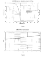
- Figure 1 shows that the precursor is thermally stable at least until 200°C; and Figure 2 shows that it presents sufficient volatility for vapour phase distribution 1100 Pa (8 Torr) at 100°C.
- [Me 2 InOtBu)] 2 is thermally stable and has a good volatility at the same time in addition of the fact that it is not a pyrophoric compound.
- a sampling is performed in a glovebox under argon with a controlled level of oxygen and moisture (below 5 ppm). 250mg of powder are placed in a small glass crystallizer. The crystallizer is then placed in a leak proof screw cap jar during the transfer from the glovebox to a fume hood. The screw cap jar is opened under the fume hood and the crystallizer with the powder in placed directly in contact with air. No fumes are seen but there are some odours of amina (HNMe 2 ). After 1 min, some drops of water are deposited directly on the product. Some bubbles are seen on the powder but without violent reaction.
- HNMe 2 amina
Landscapes
- Chemical & Material Sciences (AREA)
- Organic Chemistry (AREA)
- Chemical Vapour Deposition (AREA)
Abstract
A method for forming an indium containing thin film on a substrate comprising at least the steps of:
a) providing a vapor comprising at least one precursor compound of the formula (I): [(Ra)(Rb)ln(ORc)]2, wherein:
- Ra and Rb are independently selected in the group consisting of H, C1-C6 linear or branched alkyl, aryl or alkylsilyl;
- Rc is selected in the group consisting of C1-C4 linear or branched alkyl, aryl or alkylsilyl;
b) reacting the vapor comprising the at least one compound of formula (I) with the substrate, according to an atomic layer deposition process, to form a layer of an indium-containing complex on at least one surface of said substrate.
a) providing a vapor comprising at least one precursor compound of the formula (I): [(Ra)(Rb)ln(ORc)]2, wherein:
- Ra and Rb are independently selected in the group consisting of H, C1-C6 linear or branched alkyl, aryl or alkylsilyl;
- Rc is selected in the group consisting of C1-C4 linear or branched alkyl, aryl or alkylsilyl;
b) reacting the vapor comprising the at least one compound of formula (I) with the substrate, according to an atomic layer deposition process, to form a layer of an indium-containing complex on at least one surface of said substrate.
Description
- The present invention concerns new compounds containing Indium and a method for forming an Indium containing thin film.
- Indium is a rare metal which is most commonly recovered from the zinc-sulfide mineral sphalerite. Despite its rarity, indium is used in multitude of technical applications from electronic to photovoltaic and optical devices. Indium is dominantly used in indium tin oxide layers (ITO) for flat panel displays, copper-indium-selenide (CIS) type of solar cells, indium-gallium-nitride (InGaN) as used for LEDs; blue-ray lasers and InGaP for optoelectronic devices. In contrast to ITO and CIS that are mainly deposited by PVD, InGaN is mainly deposited by metal-organic chemical vapor deposition (MOCVD).
- In addition to above utilizations, indium can also be used for other applications. The usage of In2S3 to replace CdS in a photovoltaic CIS based stack: CIS/CdS/ZnO/ZnO:Al to obtain a better cell efficiency is already known. Indium is also reported to be used in phase-change materials (PCM) such as Ge2Sb2Te5 (GST), to form indium containing GST alloys to improve PCM characteristics such as data retention. Indium can also be used in other PCM as In-Ge-Te (IGT), In-Sb-Te (IST), or AglnSbTe. Alternatively, ln2Se3 might be used for PCM fabrication. It is known that ln2Se3 has a wider variation in electrical resistivity in comparison with the previous Ge2Sb2Te5 and therefore could be an alternative to GST.
- MOCVD and ALD are common techniques to deposit thin films that can also be used for GST depositions. These techniques require ideally stable and volatile precursors. Concerning indium precursors several sources of indium are described in literature:
- The deposition of InGaN by MOCVD from trimethylindium (TMI) is disclosed. Deposition from TMI of GalnP is already known. TMI is very volatile and reactive but is a pyrophoric compound. This last characteristic complicates its handling which requires special safety procedures.
- InCl3 and InCl are probably the most simple indium precursors but their lack of volatility (sublimation of InCl3: 133 Pa at 356°C) is a significant disadvantage. Another drawback is the generation of chlorine during deposition. Cl2 will damage the deposited layer.
- InCp is another commercial indium source. This molecule is volatile but its main disadvantage is its heat sensitivity. Heating is necessary for vaporizing the compound and therefore decomposition will occur and a clogging of the distribution line is expected.
- In(N3)3Py3 was characterized by TGA in the literature, to check the feasibility of using for InN deposition by MOCVD. It appears that the precursor decomposes firstly at 120°C and detonates at 300°C. In a safety point of view, this behavior is not acceptable for an industrial usage.
- For InS deposition, the use of Indium acetylacetonate is known, but thermal analysis of this precursor shows a high level of residues after complete vaporization. This phenomenon will generate particles and clogging in the distribution lines.
- In conclusion, there are no suitable non-pyrophoric indium metal-organic compounds with the desired thermal behavior to enable the vapor phase deposition of indium containing thin films.
- According to a first embodiment, the invention relates to compounds of formula [(Ra)(Rb)ln(ORc)]x, wherein Ra and Rb are independently selected in the group consisting of H, C1-C6 linear or branched alkyl, aryl or alkylsilyl; Rc is selected in the group consisting of C1-C4 linear or branched alkyl, aryl or alkylsilyl and x can is an integer equal to 1 or 2.
- According to another embodiment, the invention relates to the following compounds: [Me2ln(OMe)]2, [Me2ln(OtBu)]2, [Et2ln(OtBu)]2, [Me2ln(OiPr)]2, [Me2ln(OEt)]2.
- According to another embodiment, the invention concerns a method for forming an indium containing thin film on a substrate comprising at least the steps of:
- a) providing a vapor comprising at least one precursor compound of the formula (I): [(Ra)(Rb)In(ORc)]2, wherein:
- Ra and Rb are independently selected in the group consisting of H, C1-C6 linear or branched alkyl, aryl or alkylsilyl;
- Rc is selected in the group consisting of C1-C4 linear or branched alkyl, aryl or alkylsilyl;
- b)reacting the vapor comprising the at least one compound of formula (I) with the substrate, according to an atomic layer deposition process, to form a layer of an indium-containing complex on at least one surface of said substrate.
- According to another embodiment, the invention concerns a method as defined above, wherein Ra and Rb are a methyl or an ethyl group.
- According to another embodiment, the invention concerns a method as defined above, wherein Rc is chosen between methyl, tert-butyl, isopropyl and ethyl.
- According to another embodiment, the invention concerns a method as defined above, wherein the at least one precursor compound of the formula (I) is selected in the list of compounds as defined above.
- According to another embodiment, the invention concerns a method as defined above, further comprising the step:
- c) reaction of the complex formed obtained in step b) with a reagent selected from another metal source, reducing reactants and/or nitriding reactants and/or oxidizing reactants.
- According to another embodiment, the invention concerns a method of manufacturing a semiconductor structure, comprising the steps of the method defined above, wherein the substrate is a semiconductor substrate.
- According to another embodiment, the invention concerns a method of manufacturing a photovoltaic structure, comprising the steps of the method defined above, wherein the substrate is a photovoltaic substrate.
- According to another embodiment, the invention concerns the use of at least one compound of formula (I), preferably one compound selected among [Me2In(OMe)]2, [Me2In(OtBu)]2, [Et2In(OtBu)]2, [Me2In(OiPr)]2, [Me2In(OEt)]2 for the manufacturing of phase change materials (PCM).
- The new indium metal-organic compounds present at least the following features:
- 1) controlling the steric bulk of Rc will enable to form monomeric compounds;
- 2) being liquid or being easily sublimized or having a melting point below 180°C;
- 3) being thermally stable (see
figure 1 ); - 4) having sufficient volatility for vapor phase distribution (see
figure 2 ); - 5) enabling the deposition by ALD of indium containing thin films such as In-doped GST, In2Se3, InGaN,...
- 6) avoiding the pyrophoricity.
- The present invention introduces the using of a low melting point, volatile and thermally stable indium compounds to deposit indium containing thin films by either ALD process.
- According to another embodiment of the invention, the family of indium precursor of the present invention can be used for the deposition of indium containing thin films by (MO)CVD (Metal-Organic Chemical Vapor Deposition) and derivatives. Surprisingly, this novel family of metal-organic compounds presents particularly attractive thermal properties. As a matter of fact, the new precursors present the advantages of:
- 1) being liquid at room temperature or having a melting point lower than 180°C;
- 2) being thermally stable enough to enable proper distribution (gas phase or direct liquid injection) without particles generation;
- 3) being thermally stable enough to allow wide self-limited ALD window (see
figure 1 ); - 4) allowing to deposit a variety of indium containing thin films, including binary, ternary or quaternary materials. Indium can also be used as dopant. To obtain a thin film with the expected composition and physical properties, the precursor can be used in combination with a co-reactant or combination of co-reactants. The co-reactants are selected without limitation among the group consisting of O2, Plasma O2, H2O, O3, N2, NH3, hydrazine and alkyl derivatives, N-containing radicals (for instance N., NH., NH2.), NO, N2O, NO2, amines, GeCl2, SbCl3, TeCl4,TDMAGe, TDMASb, DIPT...;
- 5) having sufficient volatility for vapor phase distribution (see
figure 2 ); - 6) enabling the deposition by ALD of indium containing thin films such as In-doped GST, In2Se3, InGaN,...
- Those skilled in the art will recognize that the novel metal-organic compounds could be used in various applications fields such as electronic, photovoltaic, optoelectronic devices.
- The deposition of an indium containing film is performed in several steps:
- a. Vaporizing an indium source to form a gas-phase indium source.
- b. Introducing several precursors in vapor phase in a deposition device, wherein said precursors comprise said vaporized indium source, and may comprise another metal source, an oxygen source, a nitrogen source, a germanium source, an antimony source, a tellurium source or a selenium source to form an indium containing film.
- 1. In one embodiment of the invention, the precursor is stored in a heated canister. The vaporization of the precursor can be realized by introducing a gas in the said canister. The canister is preferably heated at a temperature which allows liquefying or subliming the said precursor with a sufficient vapor pressure. The carrier gas can be selected, from Ar, He, H2, N2 or mixtures of them. The carrier gas flow is in the range of 1 mL/min to 1 L/min. The canister can for instance be heated at temperatures in the range of 20°C to 180°C. The temperature can be adjusted to control the amount of precursor in the gas phase.
- 2. In one embodiment of the invention, the precursor is stored in a heated canister. The vaporization of the precursor can be realized by drawing the vapour to the reactor chamber without using a carrier gas flow.
- 3. In another embodiment of the invention, the said precursor source is fed in the liquid state to a vaporizer where it is vaporized.
- 4. In another embodiment, the said precursor can be mixed with a stabilizer.
- 5. The said precursor source can be mixed to a solvent or a mixture of solvent. The said solvent can be selected from the group consisting of octane, hexane, pentane, tetramethylsilane, mesithylene, and other aromatic solvents. This mixture is contained in a canister which can be heated at a temperature in the range of 20°C to 180°C.
- 6. In another embodiment of the invention, the said precursor source can be mixed to a solvent or a mixture of solvents and one or more other metal source. The said solvent can be selected from the group consisting of octane, hexane, pentane, tetramethylsilane, mesithylene and other aromatic solvents. This mixture is contained in a canister which can be heated at a temperature in the range of 20°C to 180°C.
- 7. In another embodiment of the invention, the said mixtures are fed in the liquid state to a vaporizer where they are vaporized.
- 8. In another embodiment of the invention, the said mixtures can be mixed with a stabilizer.
- 9. In one embodiment of the invention, the pressure in the said canister is in the range from 0.1 Pa to 101300 Pa (related to 1 to 4).
- 10. In one embodiment of the invention, the pressure in the said canister is in the range from 100000 Pa to 400000 Pa (related to 5 to 7).
- 11. The said vaporized metal source is introduced into a reaction chamber where it is contacted to a substrate. The substrate can be selected from the group consisting of Si, SiO2, SiN, SiON, and other metal containing films. The substrate can be heated to sufficient temperature to obtain the desired film at sufficient growth rate and with desired physical state and composition. Typical temperature range from 50°C to 600°C. Preferably the temperature is lower or equal to 450°C. The pressure in the reaction chamber is controlled to obtain the desired metal containing film at sufficient growth rate. Typical pressure range from 0.1 Pa to 13300 Pa or higher. The metal source gas flow is in the range of 1 mL/min to 1 L/min.
- 12. In one embodiment of the invention, the said new precursor source or the mixture described in 4, 5, 6, and 8 is mixed to one or more reactant species prior to the reaction chamber.
- 13. In one embodiment of the invention, the said new precursor source or the mixture described in 4, 5, 6, and 8 is mixed to one or more reactant species in the reaction chamber.
- 14. In another embodiment of the invention, the said new precursor and the reactant species can be introduced simultaneously (chemical vapor deposition), sequentially (atomic layer deposition) or different combinations. One example is to introduce metal source and the other metal source together in one pulse and co-reactant in a separate pulse (modified atomic layer deposition); another example is to introduce the reactant species (one example could be oxygen) continuously and to introduce metal source by pulse (pulsed-chemical vapor deposition). Typical temperature range from 50°C to 600°C. Preferably the temperature is lower or equal to 450°C. The pressure in the reaction chamber is controlled to obtain the desired metal containing film at sufficient growth rate. Typical pressure range from 10.1 Pa to 13300 Pa or higher. For each reactant, the gas flow is in the range of 1 mL/min to 1 L/min.
- 15. In one embodiment of the invention, the reactant species are passed through a plasma system localized remotely from the reaction chamber, and decomposed to radicals.
- 16. In one embodiment of the invention where the targeted metal based film contains oxygen, such as for example In2O3 the said reactant species include an oxygen source which is selected from, but not limited to, oxygen (O2), oxygen radicals (for instance O. or OH.), for instance generated by a remote plasma, ozone (O3), moisture (H2O) and H2O2.
- 17. In one embodiment of the invention where the targeted metal based film contains nitrogen such as InGaN, one or more reactant species containing nitrogen can be used. The said reactant species are selected from, but not limited to, nitrogen (N2), ammonia, hydrazine and alkyl derivatives, N-containing radicals (for instance N., NH., NH2.), NO, N2O, NO2, amines.
- 18. In one embodiment of the invention, the said metal sources are simultaneously introduced and mixed into the reaction chamber.
- 19. In another embodiment of the invention, the said metal sources are simultaneously introduced and mixed to reactant species into the reaction chamber.
- 20. In one embodiment of the invention, the other metal sources are selected in the group of, but without limitation, GeCl2, SbCl3, TeCl4, TDMAGe, TDMASb, DIPT...
- 21. In one embodiment of the invention, the said precursor is used for atomic layer deposition of indium containing films. The said indium source, the possible said metal source and the reactant species are introduced sequentially in the reaction chamber (atomic layer deposition). The reactor pressure is selected in the range from 0.1 Pa to 13300 Pa. Preferably, the reactor pressure is comprised between 133 Pa and 1330 Pa. A purge gas is introduced between the metal source pulse and the reactant species pulse. The purge gas can be selected without limitation from the group consisting of N2, Ar, He. The purge gas flow is in the range 100mL/min to 10L/min. The metal source, purge gas and reactant species pulse duration is comprised between 0.1 sand 100 s. Preferably, the pulse duration is comprised between 0.5 s and 10 s.
- 22. In another embodiment of the invention, the deposition of the indium containing thin film is performed by a combination of the previous elements (
points 1 to 21).
- All operations are carried in an inert gas filled glove box. 0.522g (7.04 mmol) of tBuOH are dissolved in 4 mL of Et2O. 1.48g (7.04 mmol) of Me2InC5H5 are dissolved in approximately 10 mL of Et2O. The solution of tBuOH/Et2O is added to Me2InC5H5. The mixture is stirred for 1h at room temperature before the volatile materials are removed by distillation under vacuum. A sublimation at 35°C leads to 1.51 g of Me2In(OtBu) as a colorless waxy solid.
- The indium oxide is deposited at 180°C on a sapphire substrate using [Me2In(OtBu)]2 and ozone as reactive gas. The precursor is stored into canisters and sublimed at 50°C. N2 is used as carrier gas. The precursor and reactive gas are sequentially introduced into the reactor. A film of indium oxide is obtained.
-
Figure 1 shows that the precursor is thermally stable at least until 200°C; andFigure 2 shows that it presents sufficient volatility for vapour phase distribution 1100 Pa (8 Torr) at 100°C. - Consequently, [Me2InOtBu)]2 is thermally stable and has a good volatility at the same time in addition of the fact that it is not a pyrophoric compound.
- A sampling is performed in a glovebox under argon with a controlled level of oxygen and moisture (below 5 ppm). 250mg of powder are placed in a small glass crystallizer. The crystallizer is then placed in a leak proof screw cap jar during the transfer from the glovebox to a fume hood. The screw cap jar is opened under the fume hood and the crystallizer with the powder in placed directly in contact with air. No fumes are seen but there are some odours of amina (HNMe2). After 1 min, some drops of water are deposited directly on the product. Some bubbles are seen on the powder but without violent reaction.
- We conclude that the product is not pyrophoric.
Claims (10)
- Compounds of formula [(Ra)(Rb)In(ORc)]x, wherein Ra and Rb are independently selected in the group consisting of H, C1-C6 linear or branched alkyl, aryl or alkylsilyl; Rc is selected in the group consisting of C1-C4 linear or branched alkyl, aryl or alkylsilyl and x is an integer equal to 1 or 2.
- The following compounds: [Me2In(OMe)]2, [Me2In(OtBu)]2, [Et2In(OtBu)]2, [Me2In(OiPr)]2, [Me2In(OEt)]2.
- A method for forming an indium containing thin film on a substrate comprising at least the steps of:a) providing a vapor comprising at least one precursor compound of the formula (I): [(Ra)(Rb)In(ORc)]2, wherein:- Ra and Rb are independently selected in the group consisting of H, C1-C6 linear or branched alkyl, aryl or alkylsilyl;- Rc is selected in the group consisting of C1-C4 linear or branched alkyl, aryl or alkylsilyl;b) reacting the vapor comprising the at least one compound of formula (I) with the substrate, according to an atomic layer deposition process, to form a layer of an indium-containing complex on at least one surface of said substrate.
- Method of Claim 3, wherein Ra and Rb are a methyl or an ethyl group.
- Method of anyone of Claim 3 or 4, wherein Rc is chosen between methyl, ethyl, isopropyl and tert-butyl.
- Method of claim 3, wherein the at least one precursor compound of the formula (I) is selected in the list of compounds as defined in Claim 2.
- Method of anyone of Claims 3 to 6 further comprising the step:c) reaction of the complex formed obtained in step b) with a reagent selected from another metal source, reducing reactants and/or nitriding reactants and/or oxidizing reactants.
- A method of manufacturing a semiconductor structure, comprising the steps of the method defined in any one of Claims 3 to 7, wherein the substrate is a semiconductor substrate.
- A method of manufacturing a photovoltaic structure, comprising the steps of the method defined in any one of Claims 3 to 7, wherein the substrate is a photovoltaic substrate.
- Use of at least one compound of Claim 1 or 2 for the manufacturing of phase change materials (PCM).
Priority Applications (1)
| Application Number | Priority Date | Filing Date | Title |
|---|---|---|---|
| EP11305846A EP2540733A1 (en) | 2011-06-30 | 2011-06-30 | Deposition of indium containing thin films using new indium precursors |
Applications Claiming Priority (1)
| Application Number | Priority Date | Filing Date | Title |
|---|---|---|---|
| EP11305846A EP2540733A1 (en) | 2011-06-30 | 2011-06-30 | Deposition of indium containing thin films using new indium precursors |
Publications (1)
| Publication Number | Publication Date |
|---|---|
| EP2540733A1 true EP2540733A1 (en) | 2013-01-02 |
Family
ID=44800961
Family Applications (1)
| Application Number | Title | Priority Date | Filing Date |
|---|---|---|---|
| EP11305846A Withdrawn EP2540733A1 (en) | 2011-06-30 | 2011-06-30 | Deposition of indium containing thin films using new indium precursors |
Country Status (1)
| Country | Link |
|---|---|
| EP (1) | EP2540733A1 (en) |
Cited By (1)
| Publication number | Priority date | Publication date | Assignee | Title |
|---|---|---|---|---|
| JP2018538443A (en) * | 2015-11-25 | 2018-12-27 | ユミコア・アクチエンゲゼルシャフト・ウント・コムパニー・コマンディットゲゼルシャフトUmicore AG & Co.KG | Metalorganic vapor phase deposition using solutions of alkyl-indium compounds in hydrocarbons |
Citations (2)
| Publication number | Priority date | Publication date | Assignee | Title |
|---|---|---|---|---|
| WO2010126274A2 (en) * | 2009-04-29 | 2010-11-04 | 주식회사 메카로닉스 | Cigt thin film and method for fabricating same |
| WO2010133327A1 (en) * | 2009-05-20 | 2010-11-25 | Leibniz-Institut Für Neue Materialien Gemeinnützige Gmbh | Composition and method for producing ito powders or ito coatings |
-
2011
- 2011-06-30 EP EP11305846A patent/EP2540733A1/en not_active Withdrawn
Patent Citations (2)
| Publication number | Priority date | Publication date | Assignee | Title |
|---|---|---|---|---|
| WO2010126274A2 (en) * | 2009-04-29 | 2010-11-04 | 주식회사 메카로닉스 | Cigt thin film and method for fabricating same |
| WO2010133327A1 (en) * | 2009-05-20 | 2010-11-25 | Leibniz-Institut Für Neue Materialien Gemeinnützige Gmbh | Composition and method for producing ito powders or ito coatings |
Non-Patent Citations (2)
| Title |
|---|
| DOUGLA, T. ET AL.: "Molecular precursors for indium phosphide and synthesis of small III-V semiconductor clusters in solution", INORG. CHEM., 1991, pages 594 - 596, XP002664062 * |
| PARK, J.-H. ET AL.: "The X-ray single crystal structure of [Me2In(acac)]2 and its use as a single-source precursor for the deposition of indium oxide thin films", J. MATER. CHEM., 2001, pages 2346 - 2349, XP002664061 * |
Cited By (2)
| Publication number | Priority date | Publication date | Assignee | Title |
|---|---|---|---|---|
| JP2018538443A (en) * | 2015-11-25 | 2018-12-27 | ユミコア・アクチエンゲゼルシャフト・ウント・コムパニー・コマンディットゲゼルシャフトUmicore AG & Co.KG | Metalorganic vapor phase deposition using solutions of alkyl-indium compounds in hydrocarbons |
| JP7197357B2 (en) | 2015-11-25 | 2022-12-27 | ユミコア・アクチエンゲゼルシャフト・ウント・コムパニー・コマンディットゲゼルシャフト | Organometallic Vapor Deposition Using Solutions of Alkyl-Indium Compounds in Hydrocarbons |
Similar Documents
| Publication | Publication Date | Title |
|---|---|---|
| KR101065829B1 (en) | Amorphous GE / TE deposition method | |
| US9240319B2 (en) | Chalcogenide-containing precursors, methods of making, and methods of using the same for thin film deposition | |
| US20110262660A1 (en) | Chalcogenide-containing precursors, methods of making, and methods of using the same for thin film deposition | |
| US20090299084A1 (en) | Tellurium precursors for film deposition | |
| KR20090018629A (en) | Low Temperature Deposition of Phase Change Memory Materials | |
| KR102837861B1 (en) | Indium precursor for vapor deposition | |
| US12404585B2 (en) | Lithium precursors for deposition of lithium-containing layers, islets or clusters | |
| US8802194B2 (en) | Tellurium precursors for film deposition | |
| EP2492273A1 (en) | Deposition of gallium containing thin films using gallium alkylamide precursor | |
| CN108431295B (en) | Cobalt-containing film-forming compositions, synthesis thereof, and use in film deposition | |
| EP2492272A1 (en) | Deposition of indium containing thin films using indium alkylamide precursor | |
| KR20180098579A (en) | Manganese-containing film forming compositions, their synthesis, and their use in film deposition | |
| EP2540733A1 (en) | Deposition of indium containing thin films using new indium precursors | |
| EP2540732A1 (en) | Deposition of gallium containing thin films using new gallium precursors. | |
| KR20150097429A (en) | Precursor compositions for forming germanium antimony telurium alloy and method of forming germanium antimony telurium alloy layer using them as precursors | |
| WO2017116667A1 (en) | Iron-containing film forming compositions, their synthesis, and use in film deposition |
Legal Events
| Date | Code | Title | Description |
|---|---|---|---|
| PUAI | Public reference made under article 153(3) epc to a published international application that has entered the european phase |
Free format text: ORIGINAL CODE: 0009012 |
|
| AK | Designated contracting states |
Kind code of ref document: A1 Designated state(s): AL AT BE BG CH CY CZ DE DK EE ES FI FR GB GR HR HU IE IS IT LI LT LU LV MC MK MT NL NO PL PT RO RS SE SI SK SM TR |
|
| AX | Request for extension of the european patent |
Extension state: BA ME |
|
| STAA | Information on the status of an ep patent application or granted ep patent |
Free format text: STATUS: THE APPLICATION IS DEEMED TO BE WITHDRAWN |
|
| 18D | Application deemed to be withdrawn |
Effective date: 20130703 |