EP2536254B1 - Light emitting device and illumination apparatus having same - Google Patents
Light emitting device and illumination apparatus having same Download PDFInfo
- Publication number
- EP2536254B1 EP2536254B1 EP12171584.1A EP12171584A EP2536254B1 EP 2536254 B1 EP2536254 B1 EP 2536254B1 EP 12171584 A EP12171584 A EP 12171584A EP 2536254 B1 EP2536254 B1 EP 2536254B1
- Authority
- EP
- European Patent Office
- Prior art keywords
- light emitting
- light source
- source units
- storage unit
- emitting device
- Prior art date
- Legal status (The legal status is an assumption and is not a legal conclusion. Google has not performed a legal analysis and makes no representation as to the accuracy of the status listed.)
- Not-in-force
Links
Images

Classifications
-
- H—ELECTRICITY
- H05—ELECTRIC TECHNIQUES NOT OTHERWISE PROVIDED FOR
- H05B—ELECTRIC HEATING; ELECTRIC LIGHT SOURCES NOT OTHERWISE PROVIDED FOR; CIRCUIT ARRANGEMENTS FOR ELECTRIC LIGHT SOURCES, IN GENERAL
- H05B45/00—Circuit arrangements for operating light-emitting diodes [LED]
- H05B45/20—Controlling the colour of the light
- H05B45/24—Controlling the colour of the light using electrical feedback from LEDs or from LED modules
-
- H—ELECTRICITY
- H05—ELECTRIC TECHNIQUES NOT OTHERWISE PROVIDED FOR
- H05B—ELECTRIC HEATING; ELECTRIC LIGHT SOURCES NOT OTHERWISE PROVIDED FOR; CIRCUIT ARRANGEMENTS FOR ELECTRIC LIGHT SOURCES, IN GENERAL
- H05B45/00—Circuit arrangements for operating light-emitting diodes [LED]
- H05B45/10—Controlling the intensity of the light
- H05B45/14—Controlling the intensity of the light using electrical feedback from LEDs or from LED modules
-
- H—ELECTRICITY
- H05—ELECTRIC TECHNIQUES NOT OTHERWISE PROVIDED FOR
- H05B—ELECTRIC HEATING; ELECTRIC LIGHT SOURCES NOT OTHERWISE PROVIDED FOR; CIRCUIT ARRANGEMENTS FOR ELECTRIC LIGHT SOURCES, IN GENERAL
- H05B45/00—Circuit arrangements for operating light-emitting diodes [LED]
- H05B45/30—Driver circuits
- H05B45/37—Converter circuits
- H05B45/3725—Switched mode power supply [SMPS]
Definitions
- the present invention relates to a light emitting device using a solid state light emitting element as a light source, and an illumination apparatus using the light emitting device.
- a resistor, a transistor and one or more light emitting diodes are connected in series between a pair of main terminals, and a resistor for outputting connection information (information output resistor) is connected between a joint of the light emitting diode and one of the main terminals and an information output terminal.
- connection information information output resistor
- the information output resistors of the light emitting modules all are set to substantially the same resistance value.
- the constant current source includes a pair of output terminals connected to the pair of main terminals of the light emitting module, an input terminal to which the connection information outputted from the information output terminal is inputted, a variable constant current source whose output current is variable, and a control unit for varying the current outputted from the variable constant current source according to the connection information.
- the control unit of the constant current source determines the number of the light emitting modules connected between the main terminals on the basis of a voltage inputted to the input terminal, and varies the output current of the variable constant current source according to the number of the light emitting modules connected such that a predetermined current flows in each of the light emitting modules. Accordingly, despite changes in the number of the light emitting modules connected between the main terminals of the constant current source, a predetermined current (e.g., a rated current) can flow constantly in each light emitting module.
- a predetermined current e.g., a rated current
- the light emitting module is composed of three types of light emitting diodes including, e.g., red light emitting diodes, green light emitting diodes and blue light emitting diodes, and luminous color can be changed by individually driving the light emitting diodes.
- the solid state light emitting element such as a light emitting diode tends to have a large variation in light output due to a difference in the use environment or the production lot compared with other light sources such as fluorescent lamps.
- the solid state light emitting element such as a light emitting diode
- Document DE 20 2004 006 292 U1 discloses a device for driving LEDs comprising a drive module, a LED module controlled by the drive module and a module identification channel for transferring information of the LED module to the drive module.
- Document US 2004/090189 A1 discloses an electric power supply system for LED lighting unit comprising an LED lighting unit, which includes an LED conducting circuit with an LED and a resistor, wherein the power supply system supplies a control current in a range not over the maximum allowable current of the LED conducting circuit set based on the resistance of the resistor.
- the present invention provides a light emitting device capable of suppressing a variation of light output due to individual differences in solid state light emitting elements, wherein the light emitting device adjusts the drive current supplied to each of light source units according to a rank of the light emitting device, and an illumination apparatus using the same.
- a light emitting device which includes a set of light source units including multiple types of solid state light emitting elements having different light colors, each of the light source units comprising the same type of the solid state light emitting elements connected in series and; and an information storage unit which stores information about electrical characteristic of the set of light source units, wherein the information stored in the information storage unit represents a relationship between a light output and a drive current in the set of light source units.
- the information storage unit may include one or more resistive elements having a resistance value corresponding to the information.
- the information storage unit includes the resistive elements; and switch elements which separately switches on and off conduction of the resistive elements.
- an illumination apparatus including one of the above described light emitting devices; a power supply unit which individually supplies a drive current to each of the light source units of the light emitting device; and an adjusting unit which obtains the information stored in the information storage unit, and adjusts the drive current supplied from the power supply unit to each of the light source units based on the obtained information.
- a light emitting device and an illumination apparatus using a light emitting diode as a solid state light emitting element in accordance with embodiments of the present invention will be described in detail.
- the technical concept of the present invention can be applied to a light emitting device and an illumination apparatus using a solid state light emitting element such as an organic electroluminescence (EL) element other than the light emitting diode, without being limited to those using the light emitting diode.
- EL organic electroluminescence
- an illumination apparatus in accordance with a first embodiment of the present invention includes a light emitting device 1, a lighting unit 2, and terminal blocks 3A, 3B and 3C.
- the light emitting device 1 includes three light source units 10A, 10B and 10C and an information storage unit 11.
- the light source unit 10A includes a plurality of red light emitting diodes connected in series.
- the light source unit 10B includes a plurality of green light emitting diodes connected in series.
- the light source unit 10C includes a plurality of blue light emitting diodes connected in series.
- red light, green light and blue light emitted from the light source units 10A, 10B and 10C are mixed to produce a color of light, e.g., white light, depending on a ratio of the amounts of the red, green and blue lights.
- both ends of the light source units 10A, 10B and 10C are connected to the terminal blocks 3A, 3B and 3C, respectively.
- the information storage unit 11 is formed of, e.g., resistive elements, which is set to a resistance value corresponding to a rank to which a group including the light source units 10A, 10B and 10C belongs, as will be described later. Further, both ends of the information storage unit 11, i.e., both ends of the resistive element, are connected to one end of the terminal block 3A connected to a positive terminal of the light source unit 10A and a terminal block 3D.
- the lighting unit 2 includes a power supply unit 20, an adjusting unit 21, a filter circuit 22, a rectifier circuit 23 and the like.
- An AC voltage and current supplied from a commercial AC power source 100 is filtered by the filter circuit 22, rectified by the rectifier circuit 23, and inputted to the power supply unit 20.
- the power supply unit 20 includes, e.g., a step-up chopper circuit for power factor improvement, three step-down chopper circuits for stepping down a DC voltage outputted from the step-up chopper circuit and outputting the stepped-down voltage, and four drive circuits for driving the step-up chopper circuit and the three step-down chopper circuits respectively.
- Output terminals of the three step-down chopper circuits are connected the terminal blocks 3A, 3B and 3C in a one-to-one manner, so that a drive current is individually supplied to each of the light source units 10A, 10B and 10C from each step-down chopper circuit.
- the drive circuits of the step-down chopper circuits perform pulse-width modulation (PWM) control on switching elements constituting the step-down chopper circuits, and vary the light amount of each of the light source units 10A, 10B and 10C by increasing or decreasing the drive current supplied to each of the light source units 10A, 10B and 10C.
- PWM pulse-width modulation
- the adjusting unit 21 adjusts the drive current of each of the light source units 10A, 10B and 10C by controlling the power supply unit 20 to produce a desired light color (e.g., white). That is, the adjusting unit 21 outputs a dimming signal (PWM signal) to the drive circuit of each of the step-down chopper circuits of the power supply unit 20. Each drive circuit performs PWM control on the step-down chopper circuit according to the dimming signal, so that a target drive current can be supplied to each of the light source units 10A, 10B and 10C.
- PWM signal dimming signal
- the adjusting unit 21 obtains the information stored in the information storage unit 11 of the light emitting device 1 through the terminal block 3D, and adjusts the drive current supplied to each of the light source units 10A, 10B and 10C from the power supply unit 20 based on the obtained information.
- the adjusting unit 21 may be realized, e.g., by executing a program for adjustment of the drive current in a microcomputer.
- a rank is given to a set of three types of the light source units 10A, 10B and 10C having a different emission color from each other.
- a percentage of the light amount emitted from each of the red light source unit 10A, the green light source unit 10B and the blue light source unit 10C is uniquely determined, and it is possible to determine a target value of the drive current flowing into each of the light source units 10A, 10B and 10C according to the percentage.
- the error is in the range of +1 to +3%, it is determined that the light emitting device is in rank 1, if the error is in the range of +3 to +5%, it is determined that it is in rank 2, and, if the error is in the range of - 3 to -1%, it is determined that it is in rank 3. Further, if the error is in the range of -5 to -3%, it is determined that it is in rank 4, and if the error is in the range of -1 to +1%, it is determined that it is in rank 5. Then, there is provided the information storage unit 11 formed of a resistive element having a different resistance value corresponding to each of the ranks 1 to 5.
- the operation of the adjusting unit 21 in this embodiment will be described in more detail.
- the power supply unit 20 and the adjusting unit 21 of the lighting unit 2 start to operate.
- a DC current flows through the information storage unit 11 via the terminal block 3A, and a voltage drop according to the resistance value of the information storage unit 11 is inputted to the adjusting unit 21 through the terminal block 3D.
- the adjusting unit 21 obtains the information (the rank of the light emitting device 1) stored in the information storage unit 11 based on the voltage drop inputted through the terminal block 3D.
- the adjusting unit 21 adjusts the drive current supplied to each of the light source units 10A, 10B and 10C from the power supply unit 20 according to the rank of the light emitting device 1. For example, if the light emitting device 1 that is connected is in the rank 1, the adjusting unit 21 applies the dimming signal to each drive circuit to flow the drive current 3% less than the target value of the drive current flowing into each of the light source units 10A, 10B and 10C. If the light emitting device 1 that is connected is in the rank 4, the adjusting unit 21 applies the dimming signal to each drive circuit to flow the drive current 5% more than the target value of the drive current flowing into each of the light source units 10A, 10B and 10C.
- the light emitting device 1 of this embodiment includes the information storage unit 11 storing the information about the electrical characteristics of the light source units 10A, 10B and 10C, i.e., the information representing the relationship between the drive current and the light output in each of the light source units 10A, 10B and 10C.
- the adjusting unit 21 of the lighting unit 2 adjusts the drive current supplied to each of the light source units 10A, 10B and 10C from the power supply unit 20 based on the information obtained from the information storage unit 11. Therefore, it is possible to suppress variations in light output between light emitting devices 1 due to individual variations among the light emitting diodes included therein.
- the method of determining the rank of the set including the light source units 10A, 10B and 10C is not limited to that described above.
- the rank may be determined on the basis of differences in the target values and the measured values of the drive currents between the respective light source units 10A, 10B and 10C.
- the rank may be determined using a deviation in chromaticity coordinates between the target light color and the light color that is obtained when the dimming signal corresponding to the target value of the drive current for each of the light source units 10A, 10B and 10C is applied to each drive circuit.
- the light emitting device 1 may be configured such that the light source units 10A, 10B and 10C are mounted on a main substrate 12 having a substantially elliptical shape, and a mounting substrate 13 having the information storage unit 11 thereon is disposed in a rectangular opening 12A provided at the center of the main substrate 12. With this configuration, it is easy to replace the information storage unit 11 storing the information about the rank. Further, there is an advantage of simplifying a manufacturing process of the light emitting device 1.
- the information storage unit 11 may be configured with a plurality of resistive elements. For example, it is possible to identify four ranks by using at least one of the resistive element of 500 ⁇ and the resistive element of 1k ⁇ .
- a desired number of ranks can be identified by appropriately combining a plurality of resistive elements each having a specific resistance value.
- the adjusting unit 21 of the lighting unit 2 is connected to the information storage unit 11 of the light emitting device 1 via the dedicated terminal block 3D.
- a resistive element R1 as the information storage unit 11 is connected in parallel with the terminal block 3A connected to one of the light source units (e.g., 10A), which eliminates the need for the dedicated terminal block 3D.
- the same reference numerals are assigned to the same components as the first embodiment, and illustration and description thereof will be omitted.
- the power supply unit 20 includes a step-up chopper circuit 20A, three (only one shown) step-down chopper circuits 20B and their drive circuits 20C. Further, the light source units 10B and 10C, the step-down chopper circuits and drive circuits therefor, the filter circuit and rectifier circuit are not illustrated in FIG. 4 .
- the step-down chopper circuit 20B includes a series circuit of a diode D1 and a switching element Q1, and a choke coil D1.
- the series circuit of the diode D1 and the switching element Q1 is connected across an electrolytic capacitor C1 for smoothing an output of the step-up chopper circuit 20A.
- the choke coil L1 is connected between an anode of the diode D1 and a negative terminal of the terminal block 3A (i.e., the terminal connected to a cathode of the light emitting diode in the light source unit 10A).
- the operation of the step-down chopper circuit 20B is conventionally well known, a detailed description thereof is omitted.
- a series circuit of a capacitor C2, a resistor R2 and a switch SW1 is connected between the negative terminal of the terminal block 3A and the ground.
- the adjusting unit 21 performs switching control of the switching element Q1 of the step-down chopper circuit 20B through the drive circuit 20C, and turns on the switch SW1 when the switching element Q1 is off (when the step-down chopper circuit 20B is stopped).
- the switch SW1 If the switch SW1 is turned on, a voltage caused by charges charged in the electrolytic capacitor C1 is applied to the terminal block 3A, the voltage applied to the terminal block 3A is V DC ⁇ R1/(R1+R2) when a voltage across the electrolytic capacitor C1 is VDC. Further, if the voltage V DC is higher than a forward voltage V LED of the light source unit 10A (the sum of forward voltages of the light emitting diodes which are connected in series), the discharge current from the electrolytic capacitor C1 flows through the resistor R1 of the information storage unit 11 to charge the capacitor C2.
- the potential of a connection point between the capacitor C2 and the resistor R2 is represented by VDC ⁇ R2/(R1+R2), and decreases with decrease in the voltage VDC across the electrolytic capacitor C1 (see FIG. 5 ). Further, a decreasing rate (time constant) of the potential of the connection point between the capacitor C2 and the resistor R2 varies depending on the resistance value of the resistor R1(e.g., see curves A to D in FIG. 5 ).
- the ranks (curves A to D) may also be determined based on the elapsed time until the potential of the connection point between the capacitor C2 and the resistor R2 reaches a predetermined value since turning-on of the switch SW1.
- one end of the light emitting device 1 may be connected to the ground.
- the arrangement of the switching element Q1 and the diode D1 in the step-down chopper circuit 20B is opposite to that of FIG. 4 , and the series circuit of the resistor R2, the capacitor C2 and the switch SW1 is connected between a positive terminal of the terminal block 3A and a terminal of the high potential side of the electrolytic capacitor C1.
Description
- The present invention relates to a light emitting device using a solid state light emitting element as a light source, and an illumination apparatus using the light emitting device.
- In recent years, there have been provided various light emitting devices and illumination apparatuses using a solid state light emitting element such as a light emitting diode and an organic electroluminescence (EL) element as a light source. In Japanese Patent Application Publication No.
2011-9233
apparatus in which a plurality of light emitting modules (light emitting devices) are connected in parallel to a constant current source. - In the light emitting module, a resistor, a transistor and one or more light emitting diodes are connected in series between a pair of main terminals, and a resistor for outputting connection information (information output resistor) is connected between a joint of the light emitting diode and one of the main terminals and an information output terminal. The information output resistors of the light emitting modules all are set to substantially the same resistance value.
- The constant current source includes a pair of output terminals connected to the pair of main terminals of the light emitting module, an input terminal to which the connection information outputted from the information output terminal is inputted, a variable constant current source whose output current is variable, and a control unit for varying the current outputted from the variable constant current source according to the connection information.
- With the technology disclosed in Japanese Patent
Application Publication No.2011-9233
the constant current source determines the number of the light emitting modules connected between the main terminals on the basis of a voltage inputted to the input terminal, and varies the output current of the variable constant current source according to the number of the light emitting modules connected such that a predetermined current flows in each of the light emitting modules. Accordingly, despite changes in the number of the light emitting modules connected between the main terminals of the constant current source, a predetermined current (e.g., a rated current) can flow constantly in each light emitting module. - Also, there has been provided an illumination apparatus having a dimming function of varying light intensity and a toning function of changing light color. In this case, the light emitting module is composed of three types of light emitting diodes including, e.g., red light emitting diodes, green light emitting diodes and blue light emitting diodes, and luminous color can be changed by individually driving the light emitting diodes.
- However, the solid state light emitting element such as a light emitting diode tends to have a large variation in light output due to a difference in the use environment or the production lot compared with other light sources such as fluorescent lamps. For example, in case of light emitting diodes, there is a variation in the magnitude of forward current flowing when the same forward voltage is applied, thereby resulting in variations in the light output.
-
Document DE 20 2004 006 292 U1 discloses a device for driving LEDs comprising a drive module, a LED module controlled by the drive module and a module identification channel for transferring information of the LED module to the drive module. - Document
US 2004/090189 A1 discloses an electric power supply system for LED lighting unit comprising an LED lighting unit, which includes an LED conducting circuit with an LED and a resistor, wherein the power supply system supplies a control current in a range not over the maximum allowable current of the LED conducting circuit set based on the resistance of the resistor. - In view of the above, the present invention provides a light emitting device capable of suppressing a variation of light output due to individual differences in solid state light emitting elements, wherein the light emitting device adjusts the drive current supplied to each of light source units according to a rank of the light emitting device, and an illumination apparatus using
the same. - In accordance with a first aspect of the present invention, there is provided a light emitting device which includes a set of light source units including multiple types of solid state light emitting elements having different light colors, each of the light source units comprising the same type of the solid state light emitting elements connected in series and; and an information storage unit which stores information about electrical characteristic of the set of light source units, wherein the information stored in the information storage unit represents a relationship between a light output and a drive current in the set of light source units.
- In the light emitting device, the information storage unit may include one or more resistive elements having a resistance value corresponding to the information.
- Preferably, the information storage unit includes the resistive elements; and switch elements which separately switches on and off conduction of the resistive elements.
- In accordance with a second aspect of the present invention, there is provided an illumination apparatus including one of the above described light emitting devices; a power supply unit which individually supplies a drive current to each of the light source units of the light emitting device; and an adjusting unit which obtains the information stored in the information storage unit, and adjusts the drive current supplied from the power supply unit to each of the light source units based on the obtained information.
- With the present invention, it is possible to suppress variations in light output between light emitting devices due to individual variations among the light emitting diodes included therein.
- The objects and features of the present invention will become apparent from the following description of embodiments, given in conjunction with the accompanying drawings, in which:
-
FIG. 1 is a block diagram showing a light emitting device and an illumination apparatus in accordance with a first embodiment of the present invention; -
FIG. 2 is a plan view of the light emitting device shown inFig. 1 ; -
FIG. 3 is a circuit diagram illustrating a specific configuration of an information storage unit shown inFig. 1 ; -
FIG. 4 is a block diagram partially showing a light emitting device and an illumination apparatus in accordance with a second embodiment of the present invention; -
FIG. 5 is a diagram for explaining operation in accordance with the second embodiment of the present invention; and -
FIG. 6 is a block diagram partially showing another configuration of a lighting unit in the second embodiment of the present invention. - Hereinafter, a light emitting device and an illumination apparatus using a light emitting diode as a solid state light emitting element in accordance with embodiments of the present invention will be described in detail. However, the technical concept of the present invention can be applied to a light emitting device and an illumination apparatus using a solid state light emitting element such as an organic electroluminescence (EL) element other than the light emitting diode, without being limited to those using the light emitting diode.
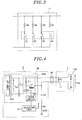
- Referring to
FIG. 1 , an illumination apparatus in accordance with a first embodiment of the present invention includes alight emitting device 1, alighting unit 2, andterminal blocks light emitting device 1 includes threelight source units information storage unit 11. Thelight source unit 10A includes a plurality of red light emitting diodes connected in series. Thelight source unit 10B includes a plurality of green light emitting diodes connected in series. Thelight source unit 10C includes a plurality of blue light emitting diodes connected in series. - Further, red light, green light and blue light emitted from the
light source units light source units terminal blocks - The
information storage unit 11 is formed of, e.g., resistive elements, which is set to a resistance value corresponding to a rank to which a group including thelight source units information storage unit 11, i.e., both ends of the resistive element, are connected to one end of theterminal block 3A connected to a positive terminal of thelight source unit 10A and aterminal block 3D. - On the other hand, the
lighting unit 2 includes apower supply unit 20, an adjustingunit 21, afilter circuit 22, arectifier circuit 23 and the like. An AC voltage and current supplied from a commercialAC power source 100 is filtered by thefilter circuit 22, rectified by therectifier circuit 23, and inputted to thepower supply unit 20. Thepower supply unit 20 includes, e.g., a step-up chopper circuit for power factor improvement, three step-down chopper circuits for stepping down a DC voltage outputted from the step-up chopper circuit and outputting the stepped-down voltage, and four drive circuits for driving the step-up chopper circuit and the three step-down chopper circuits respectively. - Output terminals of the three step-down chopper circuits are connected the
terminal blocks light source units light source units light source units power supply unit 20 is conventionally well known, detailed illustration and explanation of the circuit configuration will be omitted. - The adjusting
unit 21 adjusts the drive current of each of thelight source units power supply unit 20 to produce a desired light color (e.g., white). That is, the adjustingunit 21 outputs a dimming signal (PWM signal) to the drive circuit of each of the step-down chopper circuits of thepower supply unit 20. Each drive circuit performs PWM control on the step-down chopper circuit according to the dimming signal, so that a target drive current can be supplied to each of thelight source units - Further, the adjusting
unit 21 obtains the information stored in theinformation storage unit 11 of thelight emitting device 1 through theterminal block 3D, and adjusts the drive current supplied to each of thelight source units power supply unit 20 based on the obtained information. In addition, the adjustingunit 21 may be realized, e.g., by executing a program for adjustment of the drive current in a microcomputer. - Hereinafter, there will be described a method in which a rank is given to a set of three types of the
light source units light source unit 10A, the greenlight source unit 10B and the bluelight source unit 10C is uniquely determined, and it is possible to determine a target value of the drive current flowing into each of thelight source units - Further, since the magnitude of the drive current is adjusted by the dimming signal applied to the drive circuit of the step-down chopper circuit, the dimming signal corresponding to the target value of the drive current is applied to each drive circuit and the drive current flowing into each of the
light source units light source units - For example, if the error is in the range of +1 to +3%, it is determined that the light emitting device is in
rank 1, if the error is in the range of +3 to +5%, it is determined that it is inrank 2, and, if the error is in the range of - 3 to -1%, it is determined that it is inrank 3. Further, if the error is in the range of -5 to -3%, it is determined that it is in rank 4, and if the error is in the range of -1 to +1%, it is determined that it is in rank 5. Then, there is provided theinformation storage unit 11 formed of a resistive element having a different resistance value corresponding to each of theranks 1 to 5. - Next, the operation of the adjusting
unit 21 in this embodiment will be described in more detail. First, when theAC power source 100 is turned on after thelight emitting device 1 is connected to thelighting unit 2 via the terminal blocks 3A to 3D, thepower supply unit 20 and the adjustingunit 21 of thelighting unit 2 start to operate. When thepower supply unit 20 starts to operate, a DC current flows through theinformation storage unit 11 via theterminal block 3A, and a voltage drop according to the resistance value of theinformation storage unit 11 is inputted to the adjustingunit 21 through theterminal block 3D. The adjustingunit 21 obtains the information (the rank of the light emitting device 1) stored in theinformation storage unit 11 based on the voltage drop inputted through theterminal block 3D. - Then, the adjusting
unit 21 adjusts the drive current supplied to each of thelight source units power supply unit 20 according to the rank of thelight emitting device 1. For example, if thelight emitting device 1 that is connected is in therank 1, the adjustingunit 21 applies the dimming signal to each drive circuit to flow the drive current 3% less than the target value of the drive current flowing into each of thelight source units light emitting device 1 that is connected is in the rank 4, the adjustingunit 21 applies the dimming signal to each drive circuit to flow the drive current 5% more than the target value of the drive current flowing into each of thelight source units - As described above, the
light emitting device 1 of this embodiment includes theinformation storage unit 11 storing the information about the electrical characteristics of thelight source units light source units light emitting device 1 is connected to thelighting unit 2, the adjustingunit 21 of thelighting unit 2 adjusts the drive current supplied to each of thelight source units power supply unit 20 based on the information obtained from theinformation storage unit 11. Therefore, it is possible to suppress variations in light output between light emittingdevices 1 due to individual variations among the light emitting diodes included therein. - However, the method of determining the rank of the set including the
light source units light source units light source units - In this case, when one of the
ranks 1 to 5 as described above is given to each of light source units, total 125 ranks can be given to a set of light source units. Further, since the drive circuit supplied to each light source unit is controlled independently, it is possible to obtain the accurate target color of light. Alternatively, the rank may be determined using a deviation in chromaticity coordinates between the target light color and the light color that is obtained when the dimming signal corresponding to the target value of the drive current for each of thelight source units - Here, as shown in
FIG. 2 , thelight emitting device 1 may be configured such that thelight source units main substrate 12 having a substantially elliptical shape, and a mountingsubstrate 13 having theinformation storage unit 11 thereon is disposed in arectangular opening 12A provided at the center of themain substrate 12. With this configuration, it is easy to replace theinformation storage unit 11 storing the information about the rank. Further, there is an advantage of simplifying a manufacturing process of thelight emitting device 1. - In addition, the
information storage unit 11 may be configured with a plurality of resistive elements. For example, it is possible to identify four ranks by using at least one of the resistive element of 500Ω and the resistive element of 1kΩ. Alternatively, as shown inFIG. 3 , theinformation storage unit 11 may be constituted by a plurality of resistive elements Rj (four resistive elements R1, R2, R3 and R4 in the illustrated example) and four switch elements Sj to separately switch on and off the conduction of each of resistive elements Rj (j = 1, 2, 3, 4). A desired number of ranks can be identified by appropriately combining a plurality of resistive elements each having a specific resistance value. - In the first embodiment, the adjusting
unit 21 of thelighting unit 2 is connected to theinformation storage unit 11 of thelight emitting device 1 via the dedicatedterminal block 3D. In this embodiment, as shown inFIG. 4 , a resistive element R1 as theinformation storage unit 11 is connected in parallel with theterminal block 3A connected to one of the light source units (e.g., 10A), which eliminates the need for the dedicatedterminal block 3D. In the following description, since a basic configuration of this embodiment is almost the same as that of the first embodiment, the same reference numerals are assigned to the same components as the first embodiment, and illustration and description thereof will be omitted. - As shown in
FIG. 4 , thepower supply unit 20 includes a step-upchopper circuit 20A, three (only one shown) step-downchopper circuits 20B and theirdrive circuits 20C. Further, thelight source units FIG. 4 . - The step-down
chopper circuit 20B includes a series circuit of a diode D1 and a switching element Q1, and a choke coil D1. The series circuit of the diode D1 and the switching element Q1 is connected across an electrolytic capacitor C1 for smoothing an output of the step-upchopper circuit 20A. Further, the choke coil L1 is connected between an anode of the diode D1 and a negative terminal of theterminal block 3A (i.e., the terminal connected to a cathode of the light emitting diode in thelight source unit 10A). Herein, since the operation of the step-downchopper circuit 20B is conventionally well known, a detailed description thereof is omitted. - In the
lighting unit 2, a series circuit of a capacitor C2, a resistor R2 and a switch SW1 is connected between the negative terminal of theterminal block 3A and the ground. The adjustingunit 21 performs switching control of the switching element Q1 of the step-downchopper circuit 20B through thedrive circuit 20C, and turns on the switch SW1 when the switching element Q1 is off (when the step-downchopper circuit 20B is stopped). - If the switch SW1 is turned on, a voltage caused by charges charged in the electrolytic capacitor C1 is applied to the
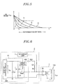
terminal block 3A, the voltage applied to theterminal block 3A is VDC×R1/(R1+R2) when a voltage across the electrolytic capacitor C1 is VDC. Further, if the voltage VDC is higher than a forward voltage VLED of thelight source unit 10A (the sum of forward voltages of the light emitting diodes which are connected in series), the discharge current from the electrolytic capacitor C1 flows through the resistor R1 of theinformation storage unit 11 to charge the capacitor C2. - At this time, the potential of a connection point between the capacitor C2 and the resistor R2 is represented by VDC×R2/(R1+R2), and decreases with decrease in the voltage VDC across the electrolytic capacitor C1 (see
FIG. 5 ). Further, a decreasing rate (time constant) of the potential of the connection point between the capacitor C2 and the resistor R2 varies depending on the resistance value of the resistor R1(e.g., see curves A to D inFIG. 5 ). - Thus, the potential of the connection point between the capacitor C2 and the resistor R2 is monitored by the adjusting
unit 21, and the ranks represented by the resistance value of the resistor R1 can be determined based on the potential at the time point when a certain time T1 has elapsed from the time point (t=0) when the switch SW1 is turned on. In addition, the ranks (curves A to D) may also be determined based on the elapsed time until the potential of the connection point between the capacitor C2 and the resistor R2 reaches a predetermined value since turning-on of the switch SW1. - On the other hand, as shown in
FIG. 6 , one end of the light emitting device 1 (one end of the cathode side of thelight source units chopper circuit 20B is opposite to that ofFIG. 4 , and the series circuit of the resistor R2, the capacitor C2 and the switch SW1 is connected between a positive terminal of theterminal block 3A and a terminal of the high potential side of the electrolytic capacitor C1. - Thus, the adjusting
unit 21 can monitor the potential of the connection point between the resistors R1 and R2, and determine the rank (curves A to D) represented by the resistance value of the resistor R1 based on the potential at the time point when a certain time T1 has elapsed from the time point (t=0) when the switch SW1 is turned on. Instead of the potential of the connection point between the resistors R1 and R2, the adjustingunit 21 may monitor the potential of the connection point between the resistor R2 and the capacitor C2. - While the invention has been shown and described with respect to the embodiments, it will be understood by those skilled in the art that various changes and modification may be made without departing from the scope of the invention as defined in the following claims.
Claims (7)
- A light emitting device (1) for an illumination apparatus with a lighting unit (2), comprising:a set of light source units (10A, 10B, 10C) including multiple types of solid state light emitting elements, each of the light source units having a different light color, and each of the light source units comprising solid state light emitting elements of the same type connected in series and; an information storage unit (11) configured to store information about electrical characteristic of the set of light source units (10A, 10B, 10C),wherein the information stored in the information storage unit represents a relationship between a light output and a drive current in the set of light source units (10A, 10B, 10C), wherein the information is provided to the lighting unit (2) to adjust the drive current supplied to each of the light source units (10A, 10B, 10C)
one end of the information storage unit (11) is connected to one of the light source units (10A, 10B, 10C) and the other end of the information storage unit (11) is connected dedicated terminal block (3D) not connected to any of the light source units (10A, 10B, 10C),
the light emitting device (1) is characterized in thatthe information storage unit (11) is formed of a resistive element having a different resistance value corresponding to one of a plurality of ranks, the light emitting device (1) is further configured to obtain the rank of the light emitting device (1) based on the voltage drop inputted through the terminal block (3D), and to adjust the drive current supplied to each of the light source units (10A, 10B, 10C) according to the rank of the light emitting device (1). - A light emitting device (1) for an illumination apparatus with a lighting unit (2), comprising:a set of light source units (10A, 10B, 10C) including multiple types of solid state light emitting elements, each of the light source units having a different light color and each of the light source units comprising solid state light emitting elements of the same type connected in series and;
an information storage unit (11) configured to store information about electrical characteristic of the set of light source units (10A, 10B, 10C),wherein the information stored in the information storage unit represents a relationship between a light output and a drive current in the set of light source units (10A, 10B, 10C), wherein the information is provided to the lighting unit (2) to adjust the drive current supplied to each of the light source units (10A, 10B, 10C),the information storage unit (11) is connected in parallel with one of the light source units (10A, 10B, 10C),
the light emitting device (1) is characterized in that
wherein a series circuit of a capacitor (C2), a resistor (R2) and a switch (SW1) is connected to one of the terminals of the information storage unit,
wherein the light emitting device (1) is configured such that,
a potential of the connection point between the capacitor (C2) and the resistor (R2) is monitored,
and a rank is determined based on the potential of the connection point at a time point when a time (T1) has elapsed from a time point when the switch (SW1) is turned on, wherein said adjustment of the drive current supplied to the light emitting device is based on said rank. - A light emitting device (1) for an illumination apparatus with a lighting unit (2), comprising:a set of light source units (10A, 10B, 10C) including multiple types of solid state light emitting elements, each of the light source units having a different light color and each of the light source units comprising solid state light emitting elements of the same type connected in series and; an information storage unit (11) configured to store information about electrical characteristic of the set of light source units (10A, 10B, 10C),wherein the information stored in the information storage unit represents a relationship between a light output and a drive current in the set of light source units (10A, 10B, 10C), wherein the information is provided to the lighting unit (2) to adjust the drive current supplied to each of the light source units (10A, 10B, 10C),the light emitting device (1) is characterized in that
the information storage unit (11) is connected in parallel with one of the light source units (10A, 10B, 10C),
wherein a series circuit of a capacitor (C2), a resistor (R2) and a switch (SW1) is connected to one of the terminals of the information storage unit,
wherein the light emitting device (1) is configured such that,
a potential of the connection point between the information storage unit (11) and the resistor (R2) is monitored,
and a rank is determined based on the potential of the connection point at a time point when a time (T1) has elapsed from a time point when the switch (SW1) is turned on, wherein said adjustment of the drive current supplied to the light emitting device is based on said rank. - The light emitting device (1) any one of claims 1 to 3, wherein the information storage unit (11) includes one or more resistive elements having a resistance value corresponding to the information.
- The light emitting device (1) of claim 4, wherein the information storage unit (11) further includes the resistive elements; and switch elements which separately switches on and off conduction of the resistive elements.
- An illumination apparatus comprising:the light emitting device (1) described in any one of claims 1 to 5;the power supply unit (20) which individually supplies a drive current to each of the light source units (10A, 10B, 10C) of the light emitting device (1); andan adjusting unit (21) which obtains the information stored in the information storage unit (11), and adjusts the drive current supplied from the power supply unit (20) to each of the light source units (10A, 10B, 10C) based on the obtained information.
- The illumination apparatus of claim 6, wherein one end of the information storage unit (11) is connected to one of the light source units (10A, 10B, 10C) and the other end of the information storage unit (11) is connected to the adjusting unit (21).
Applications Claiming Priority (1)
| Application Number | Priority Date | Filing Date | Title |
|---|---|---|---|
| JP2011133507A JP5834237B2 (en) | 2011-06-15 | 2011-06-15 | Lighting device |
Publications (2)
| Publication Number | Publication Date |
|---|---|
| EP2536254A1 EP2536254A1 (en) | 2012-12-19 |
| EP2536254B1 true EP2536254B1 (en) | 2018-09-19 |
Family
ID=46466114
Family Applications (1)
| Application Number | Title | Priority Date | Filing Date |
|---|---|---|---|
| EP12171584.1A Not-in-force EP2536254B1 (en) | 2011-06-15 | 2012-06-12 | Light emitting device and illumination apparatus having same |
Country Status (4)
| Country | Link |
|---|---|
| US (1) | US9113532B2 (en) |
| EP (1) | EP2536254B1 (en) |
| JP (1) | JP5834237B2 (en) |
| CN (1) | CN102833909B (en) |
Families Citing this family (12)
| Publication number | Priority date | Publication date | Assignee | Title |
|---|---|---|---|---|
| JP5973322B2 (en) * | 2012-10-31 | 2016-08-23 | 東芝シュネデール・インバータ株式会社 | Stored power discharge circuit of inverter device |
| CN103715894B (en) * | 2014-01-07 | 2016-08-31 | 山东大学 | A kind of multichannel adjustable great current constant current intelligent sensing control electric supply installation |
| JP6278350B2 (en) * | 2014-01-14 | 2018-02-14 | アール・ビー・コントロールズ株式会社 | LED lighting device |
| JP6206814B2 (en) | 2014-02-28 | 2017-10-04 | パナソニックIpマネジメント株式会社 | Lighting device and lighting system using the lighting device |
| JP6372776B2 (en) | 2014-03-07 | 2018-08-15 | パナソニックIpマネジメント株式会社 | Light source device, lighting device, lighting fixture |
| AT516860B1 (en) * | 2015-06-01 | 2016-09-15 | Zizala Lichtsysteme Gmbh | LED light module for a lighting device for vehicles |
| JP6654367B2 (en) * | 2015-07-08 | 2020-02-26 | シーシーエス株式会社 | Power supply device and light irradiation system including the same |
| JP2017135225A (en) * | 2016-01-27 | 2017-08-03 | シーシーエス株式会社 | Power supply device for use in led light-emitting device |
| DE102016122209A1 (en) * | 2016-11-18 | 2018-05-24 | Vishay Semiconductor Gmbh | Color mixing LED assembly and manufacturing method therefor |
| WO2018143282A1 (en) * | 2017-01-31 | 2018-08-09 | ローム株式会社 | Led drive circuit, led drive device, and led drive system |
| JP7303047B2 (en) * | 2019-06-27 | 2023-07-04 | 矢崎総業株式会社 | Light-emitting device and chromaticity variation correction method |
| WO2024068277A1 (en) * | 2022-09-27 | 2024-04-04 | Signify Holding B.V. | Smps series regulator with energy recycle back to the source |
Citations (3)
| Publication number | Priority date | Publication date | Assignee | Title |
|---|---|---|---|---|
| US20040090189A1 (en) * | 2002-10-16 | 2004-05-13 | Kenji Yoneda | Electric power supply system for LED lighting unit |
| DE202004006292U1 (en) * | 2004-04-21 | 2004-07-22 | Knobel Ag Lichttechnische Komponenten | Connection between drive stage and LED array has an identification channel for information needed for different types of LED |
| JP2006351484A (en) * | 2005-06-20 | 2006-12-28 | Moritex Corp | Illumination device and illumination head used for the same |
Family Cites Families (14)
| Publication number | Priority date | Publication date | Assignee | Title |
|---|---|---|---|---|
| EP0923067B1 (en) * | 1997-03-12 | 2004-08-04 | Seiko Epson Corporation | Pixel circuit, display device and electronic equipment having current-driven light-emitting device |
| JP2001024226A (en) * | 1999-07-07 | 2001-01-26 | Nec Saitama Ltd | Light emitting diode and displaying circuit using the same |
| JP3824603B2 (en) * | 2002-10-16 | 2006-09-20 | シーシーエス株式会社 | Power supply system for LED lighting device |
| JP2005093196A (en) * | 2003-09-17 | 2005-04-07 | Moritex Corp | Lighting method, and lighting system and component for the same |
| JP2006135007A (en) * | 2004-11-04 | 2006-05-25 | Sanyo Electric Co Ltd | Light emitting element |
| JP4516467B2 (en) * | 2005-03-29 | 2010-08-04 | シャープ株式会社 | Surface illumination device and liquid crystal display device including the same |
| TWI479466B (en) * | 2005-05-25 | 2015-04-01 | Koninkl Philips Electronics Nv | Flux compensation led driver system and method |
| JP2007042533A (en) * | 2005-08-05 | 2007-02-15 | Moritex Corp | Lighting apparatus and lighting head to be used for the apparatus |
| US7589435B2 (en) * | 2006-08-02 | 2009-09-15 | Cisco Technology, Inc. | Reporting power requirements of a powered device |
| US8011794B1 (en) * | 2007-02-13 | 2011-09-06 | American Megatrends, Inc. | Data cable powered light fixture |
| JP4951369B2 (en) * | 2007-02-23 | 2012-06-13 | パナソニック株式会社 | Lighting device and lighting system |
| US8390262B2 (en) * | 2008-11-17 | 2013-03-05 | Lepower Semiconductor Inc. | Methods and circuits for LED drivers and for PWM dimming controls |
| JP5046068B2 (en) | 2010-08-25 | 2012-10-10 | 東芝ライテック株式会社 | Lighting device |
| US8390205B2 (en) * | 2010-09-01 | 2013-03-05 | Osram Sylvania Inc. | LED control using modulation frequency detection techniques |
-
2011
- 2011-06-15 JP JP2011133507A patent/JP5834237B2/en active Active
-
2012
- 2012-06-12 EP EP12171584.1A patent/EP2536254B1/en not_active Not-in-force
- 2012-06-13 US US13/495,060 patent/US9113532B2/en not_active Expired - Fee Related
- 2012-06-15 CN CN201210202411.XA patent/CN102833909B/en not_active Expired - Fee Related
Patent Citations (3)
| Publication number | Priority date | Publication date | Assignee | Title |
|---|---|---|---|---|
| US20040090189A1 (en) * | 2002-10-16 | 2004-05-13 | Kenji Yoneda | Electric power supply system for LED lighting unit |
| DE202004006292U1 (en) * | 2004-04-21 | 2004-07-22 | Knobel Ag Lichttechnische Komponenten | Connection between drive stage and LED array has an identification channel for information needed for different types of LED |
| JP2006351484A (en) * | 2005-06-20 | 2006-12-28 | Moritex Corp | Illumination device and illumination head used for the same |
Also Published As
| Publication number | Publication date |
|---|---|
| EP2536254A1 (en) | 2012-12-19 |
| JP5834237B2 (en) | 2015-12-16 |
| US9113532B2 (en) | 2015-08-18 |
| JP2013004280A (en) | 2013-01-07 |
| US20120319602A1 (en) | 2012-12-20 |
| CN102833909B (en) | 2016-01-13 |
| CN102833909A (en) | 2012-12-19 |
Similar Documents
| Publication | Publication Date | Title |
|---|---|---|
| EP2536254B1 (en) | Light emitting device and illumination apparatus having same | |
| US9144127B1 (en) | AC-powered LED light engines, integrated circuits and illuminating apparatuses having the same | |
| JP5725736B2 (en) | LED power supply device and LED lighting apparatus | |
| US8004211B2 (en) | LED lighting device | |
| TWI432087B (en) | An arrangement for driving led cells | |
| US8183795B2 (en) | LED current-supplying circuit and LED current-controlling circuit | |
| US8063579B2 (en) | Circuit-arrangement for modulating an LED and method for operating same | |
| KR101435853B1 (en) | Apparatus for driving light emitting diode | |
| JP2012004240A (en) | Led power supply and led illumination equipment | |
| CN106455191A (en) | Lighting apparatus | |
| JP5538078B2 (en) | LED power supply | |
| CN103491670A (en) | Semiconductor-light-source control device | |
| US11019702B2 (en) | Driver and method for driving at least two sets of solid state lighting elements | |
| JP2009170917A (en) | Bi-directional light emitting diode drive circuit in bi-directional power parallel resonance | |
| US20150069914A1 (en) | Lighting Interconnection and Lighting Control Module | |
| US9532412B2 (en) | Lighting apparatus capable of reducing flicker | |
| KR102165446B1 (en) | Apparatus for driving light emitting diode | |
| JP2015506104A (en) | Light emitting device and system | |
| KR20170100916A (en) | Control circuit for lighting apparatus | |
| KR101122166B1 (en) | Smart converter that have led module realization function | |
| JPWO2014087874A1 (en) | Lighting device | |
| KR20140107837A (en) | Led lighting system and control circuit thereof | |
| TWI610595B (en) | Dimmable electrinic control gears for led light engine and application thereof | |
| KR20200134129A (en) | LED lighting apparatus and LED driving circuit thereof | |
| CN114390750A (en) | LED driving system for plant illumination and plant illumination system |
Legal Events
| Date | Code | Title | Description |
|---|---|---|---|
| PUAI | Public reference made under article 153(3) epc to a published international application that has entered the european phase |
Free format text: ORIGINAL CODE: 0009012 |
|
| AK | Designated contracting states |
Kind code of ref document: A1 Designated state(s): AL AT BE BG CH CY CZ DE DK EE ES FI FR GB GR HR HU IE IS IT LI LT LU LV MC MK MT NL NO PL PT RO RS SE SI SK SM TR |
|
| AX | Request for extension of the european patent |
Extension state: BA ME |
|
| 17P | Request for examination filed |
Effective date: 20130619 |
|
| RBV | Designated contracting states (corrected) |
Designated state(s): AL AT BE BG CH CY CZ DE DK EE ES FI FR GB GR HR HU IE IS IT LI LT LU LV MC MK MT NL NO PL PT RO RS SE SI SK SM TR |
|
| 17Q | First examination report despatched |
Effective date: 20150225 |
|
| RAP1 | Party data changed (applicant data changed or rights of an application transferred) |
Owner name: PANASONIC INTELLECTUAL PROPERTY MANAGEMENT CO., LT |
|
| STAA | Information on the status of an ep patent application or granted ep patent |
Free format text: STATUS: EXAMINATION IS IN PROGRESS |
|
| REG | Reference to a national code |
Ref country code: DE Ref legal event code: R079 Ref document number: 602012051196 Country of ref document: DE Free format text: PREVIOUS MAIN CLASS: H05B0033080000 Ipc: H05B0037020000 |
|
| GRAP | Despatch of communication of intention to grant a patent |
Free format text: ORIGINAL CODE: EPIDOSNIGR1 |
|
| STAA | Information on the status of an ep patent application or granted ep patent |
Free format text: STATUS: GRANT OF PATENT IS INTENDED |
|
| RIC1 | Information provided on ipc code assigned before grant |
Ipc: H05B 33/08 20060101ALI20180404BHEP Ipc: H05B 37/02 20060101AFI20180404BHEP |
|
| INTG | Intention to grant announced |
Effective date: 20180425 |
|
| GRAS | Grant fee paid |
Free format text: ORIGINAL CODE: EPIDOSNIGR3 |
|
| GRAA | (expected) grant |
Free format text: ORIGINAL CODE: 0009210 |
|
| STAA | Information on the status of an ep patent application or granted ep patent |
Free format text: STATUS: THE PATENT HAS BEEN GRANTED |
|
| AK | Designated contracting states |
Kind code of ref document: B1 Designated state(s): AL AT BE BG CH CY CZ DE DK EE ES FI FR GB GR HR HU IE IS IT LI LT LU LV MC MK MT NL NO PL PT RO RS SE SI SK SM TR |
|
| REG | Reference to a national code |
Ref country code: GB Ref legal event code: FG4D |
|
| REG | Reference to a national code |
Ref country code: CH Ref legal event code: EP |
|
| REG | Reference to a national code |
Ref country code: AT Ref legal event code: REF Ref document number: 1044863 Country of ref document: AT Kind code of ref document: T Effective date: 20181015 |
|
| REG | Reference to a national code |
Ref country code: IE Ref legal event code: FG4D |
|
| REG | Reference to a national code |
Ref country code: DE Ref legal event code: R096 Ref document number: 602012051196 Country of ref document: DE |
|
| REG | Reference to a national code |
Ref country code: NL Ref legal event code: MP Effective date: 20180919 |
|
| PG25 | Lapsed in a contracting state [announced via postgrant information from national office to epo] |
Ref country code: LT Free format text: LAPSE BECAUSE OF FAILURE TO SUBMIT A TRANSLATION OF THE DESCRIPTION OR TO PAY THE FEE WITHIN THE PRESCRIBED TIME-LIMIT Effective date: 20180919 Ref country code: RS Free format text: LAPSE BECAUSE OF FAILURE TO SUBMIT A TRANSLATION OF THE DESCRIPTION OR TO PAY THE FEE WITHIN THE PRESCRIBED TIME-LIMIT Effective date: 20180919 Ref country code: GR Free format text: LAPSE BECAUSE OF FAILURE TO SUBMIT A TRANSLATION OF THE DESCRIPTION OR TO PAY THE FEE WITHIN THE PRESCRIBED TIME-LIMIT Effective date: 20181220 Ref country code: SE Free format text: LAPSE BECAUSE OF FAILURE TO SUBMIT A TRANSLATION OF THE DESCRIPTION OR TO PAY THE FEE WITHIN THE PRESCRIBED TIME-LIMIT Effective date: 20180919 Ref country code: BG Free format text: LAPSE BECAUSE OF FAILURE TO SUBMIT A TRANSLATION OF THE DESCRIPTION OR TO PAY THE FEE WITHIN THE PRESCRIBED TIME-LIMIT Effective date: 20181219 Ref country code: NO Free format text: LAPSE BECAUSE OF FAILURE TO SUBMIT A TRANSLATION OF THE DESCRIPTION OR TO PAY THE FEE WITHIN THE PRESCRIBED TIME-LIMIT Effective date: 20181219 Ref country code: FI Free format text: LAPSE BECAUSE OF FAILURE TO SUBMIT A TRANSLATION OF THE DESCRIPTION OR TO PAY THE FEE WITHIN THE PRESCRIBED TIME-LIMIT Effective date: 20180919 |
|
| REG | Reference to a national code |
Ref country code: LT Ref legal event code: MG4D |
|
| PG25 | Lapsed in a contracting state [announced via postgrant information from national office to epo] |
Ref country code: HR Free format text: LAPSE BECAUSE OF FAILURE TO SUBMIT A TRANSLATION OF THE DESCRIPTION OR TO PAY THE FEE WITHIN THE PRESCRIBED TIME-LIMIT Effective date: 20180919 Ref country code: LV Free format text: LAPSE BECAUSE OF FAILURE TO SUBMIT A TRANSLATION OF THE DESCRIPTION OR TO PAY THE FEE WITHIN THE PRESCRIBED TIME-LIMIT Effective date: 20180919 Ref country code: AL Free format text: LAPSE BECAUSE OF FAILURE TO SUBMIT A TRANSLATION OF THE DESCRIPTION OR TO PAY THE FEE WITHIN THE PRESCRIBED TIME-LIMIT Effective date: 20180919 |
|
| REG | Reference to a national code |
Ref country code: AT Ref legal event code: MK05 Ref document number: 1044863 Country of ref document: AT Kind code of ref document: T Effective date: 20180919 |
|
| PG25 | Lapsed in a contracting state [announced via postgrant information from national office to epo] |
Ref country code: CZ Free format text: LAPSE BECAUSE OF FAILURE TO SUBMIT A TRANSLATION OF THE DESCRIPTION OR TO PAY THE FEE WITHIN THE PRESCRIBED TIME-LIMIT Effective date: 20180919 Ref country code: IT Free format text: LAPSE BECAUSE OF FAILURE TO SUBMIT A TRANSLATION OF THE DESCRIPTION OR TO PAY THE FEE WITHIN THE PRESCRIBED TIME-LIMIT Effective date: 20180919 Ref country code: RO Free format text: LAPSE BECAUSE OF FAILURE TO SUBMIT A TRANSLATION OF THE DESCRIPTION OR TO PAY THE FEE WITHIN THE PRESCRIBED TIME-LIMIT Effective date: 20180919 Ref country code: EE Free format text: LAPSE BECAUSE OF FAILURE TO SUBMIT A TRANSLATION OF THE DESCRIPTION OR TO PAY THE FEE WITHIN THE PRESCRIBED TIME-LIMIT Effective date: 20180919 Ref country code: NL Free format text: LAPSE BECAUSE OF FAILURE TO SUBMIT A TRANSLATION OF THE DESCRIPTION OR TO PAY THE FEE WITHIN THE PRESCRIBED TIME-LIMIT Effective date: 20180919 Ref country code: AT Free format text: LAPSE BECAUSE OF FAILURE TO SUBMIT A TRANSLATION OF THE DESCRIPTION OR TO PAY THE FEE WITHIN THE PRESCRIBED TIME-LIMIT Effective date: 20180919 Ref country code: ES Free format text: LAPSE BECAUSE OF FAILURE TO SUBMIT A TRANSLATION OF THE DESCRIPTION OR TO PAY THE FEE WITHIN THE PRESCRIBED TIME-LIMIT Effective date: 20180919 Ref country code: PL Free format text: LAPSE BECAUSE OF FAILURE TO SUBMIT A TRANSLATION OF THE DESCRIPTION OR TO PAY THE FEE WITHIN THE PRESCRIBED TIME-LIMIT Effective date: 20180919 Ref country code: IS Free format text: LAPSE BECAUSE OF FAILURE TO SUBMIT A TRANSLATION OF THE DESCRIPTION OR TO PAY THE FEE WITHIN THE PRESCRIBED TIME-LIMIT Effective date: 20190119 |
|
| PG25 | Lapsed in a contracting state [announced via postgrant information from national office to epo] |
Ref country code: SK Free format text: LAPSE BECAUSE OF FAILURE TO SUBMIT A TRANSLATION OF THE DESCRIPTION OR TO PAY THE FEE WITHIN THE PRESCRIBED TIME-LIMIT Effective date: 20180919 Ref country code: PT Free format text: LAPSE BECAUSE OF FAILURE TO SUBMIT A TRANSLATION OF THE DESCRIPTION OR TO PAY THE FEE WITHIN THE PRESCRIBED TIME-LIMIT Effective date: 20190119 Ref country code: SM Free format text: LAPSE BECAUSE OF FAILURE TO SUBMIT A TRANSLATION OF THE DESCRIPTION OR TO PAY THE FEE WITHIN THE PRESCRIBED TIME-LIMIT Effective date: 20180919 |
|
| REG | Reference to a national code |
Ref country code: DE Ref legal event code: R097 Ref document number: 602012051196 Country of ref document: DE |
|
| PLBE | No opposition filed within time limit |
Free format text: ORIGINAL CODE: 0009261 |
|
| STAA | Information on the status of an ep patent application or granted ep patent |
Free format text: STATUS: NO OPPOSITION FILED WITHIN TIME LIMIT |
|
| PG25 | Lapsed in a contracting state [announced via postgrant information from national office to epo] |
Ref country code: DK Free format text: LAPSE BECAUSE OF FAILURE TO SUBMIT A TRANSLATION OF THE DESCRIPTION OR TO PAY THE FEE WITHIN THE PRESCRIBED TIME-LIMIT Effective date: 20180919 |
|
| PGFP | Annual fee paid to national office [announced via postgrant information from national office to epo] |
Ref country code: DE Payment date: 20190619 Year of fee payment: 8 |
|
| 26N | No opposition filed |
Effective date: 20190620 |
|
| PG25 | Lapsed in a contracting state [announced via postgrant information from national office to epo] |
Ref country code: SI Free format text: LAPSE BECAUSE OF FAILURE TO SUBMIT A TRANSLATION OF THE DESCRIPTION OR TO PAY THE FEE WITHIN THE PRESCRIBED TIME-LIMIT Effective date: 20180919 |
|
| PG25 | Lapsed in a contracting state [announced via postgrant information from national office to epo] |
Ref country code: MC Free format text: LAPSE BECAUSE OF FAILURE TO SUBMIT A TRANSLATION OF THE DESCRIPTION OR TO PAY THE FEE WITHIN THE PRESCRIBED TIME-LIMIT Effective date: 20180919 |
|
| REG | Reference to a national code |
Ref country code: CH Ref legal event code: PL |
|
| GBPC | Gb: european patent ceased through non-payment of renewal fee |
Effective date: 20190612 |
|
| REG | Reference to a national code |
Ref country code: BE Ref legal event code: MM Effective date: 20190630 |
|
| PG25 | Lapsed in a contracting state [announced via postgrant information from national office to epo] |
Ref country code: TR Free format text: LAPSE BECAUSE OF FAILURE TO SUBMIT A TRANSLATION OF THE DESCRIPTION OR TO PAY THE FEE WITHIN THE PRESCRIBED TIME-LIMIT Effective date: 20180919 |
|
| PG25 | Lapsed in a contracting state [announced via postgrant information from national office to epo] |
Ref country code: GB Free format text: LAPSE BECAUSE OF NON-PAYMENT OF DUE FEES Effective date: 20190612 Ref country code: IE Free format text: LAPSE BECAUSE OF NON-PAYMENT OF DUE FEES Effective date: 20190612 |
|
| PG25 | Lapsed in a contracting state [announced via postgrant information from national office to epo] |
Ref country code: LU Free format text: LAPSE BECAUSE OF NON-PAYMENT OF DUE FEES Effective date: 20190612 Ref country code: BE Free format text: LAPSE BECAUSE OF NON-PAYMENT OF DUE FEES Effective date: 20190630 Ref country code: CH Free format text: LAPSE BECAUSE OF NON-PAYMENT OF DUE FEES Effective date: 20190630 Ref country code: LI Free format text: LAPSE BECAUSE OF NON-PAYMENT OF DUE FEES Effective date: 20190630 |
|
| PG25 | Lapsed in a contracting state [announced via postgrant information from national office to epo] |
Ref country code: FR Free format text: LAPSE BECAUSE OF NON-PAYMENT OF DUE FEES Effective date: 20190630 |
|
| REG | Reference to a national code |
Ref country code: DE Ref legal event code: R119 Ref document number: 602012051196 Country of ref document: DE |
|
| PG25 | Lapsed in a contracting state [announced via postgrant information from national office to epo] |
Ref country code: CY Free format text: LAPSE BECAUSE OF FAILURE TO SUBMIT A TRANSLATION OF THE DESCRIPTION OR TO PAY THE FEE WITHIN THE PRESCRIBED TIME-LIMIT Effective date: 20180919 Ref country code: DE Free format text: LAPSE BECAUSE OF NON-PAYMENT OF DUE FEES Effective date: 20210101 |
|
| PG25 | Lapsed in a contracting state [announced via postgrant information from national office to epo] |
Ref country code: MT Free format text: LAPSE BECAUSE OF FAILURE TO SUBMIT A TRANSLATION OF THE DESCRIPTION OR TO PAY THE FEE WITHIN THE PRESCRIBED TIME-LIMIT Effective date: 20180919 Ref country code: HU Free format text: LAPSE BECAUSE OF FAILURE TO SUBMIT A TRANSLATION OF THE DESCRIPTION OR TO PAY THE FEE WITHIN THE PRESCRIBED TIME-LIMIT; INVALID AB INITIO Effective date: 20120612 |
|
| PG25 | Lapsed in a contracting state [announced via postgrant information from national office to epo] |
Ref country code: MK Free format text: LAPSE BECAUSE OF FAILURE TO SUBMIT A TRANSLATION OF THE DESCRIPTION OR TO PAY THE FEE WITHIN THE PRESCRIBED TIME-LIMIT Effective date: 20180919 |