EP2535940A1 - Bipolar diode and method for manufacturing the same - Google Patents
Bipolar diode and method for manufacturing the same Download PDFInfo
- Publication number
- EP2535940A1 EP2535940A1 EP11169792A EP11169792A EP2535940A1 EP 2535940 A1 EP2535940 A1 EP 2535940A1 EP 11169792 A EP11169792 A EP 11169792A EP 11169792 A EP11169792 A EP 11169792A EP 2535940 A1 EP2535940 A1 EP 2535940A1
- Authority
- EP
- European Patent Office
- Prior art keywords
- ions
- anode
- depth
- layer
- wafer
- Prior art date
- Legal status (The legal status is an assumption and is not a legal conclusion. Google has not performed a legal analysis and makes no representation as to the accuracy of the status listed.)
- Granted
Links
Images


Classifications
-
- H—ELECTRICITY
- H10—SEMICONDUCTOR DEVICES; ELECTRIC SOLID-STATE DEVICES NOT OTHERWISE PROVIDED FOR
- H10D—INORGANIC ELECTRIC SEMICONDUCTOR DEVICES
- H10D8/00—Diodes
- H10D8/422—PN diodes having the PN junctions in mesas
-
- H—ELECTRICITY
- H10—SEMICONDUCTOR DEVICES; ELECTRIC SOLID-STATE DEVICES NOT OTHERWISE PROVIDED FOR
- H10D—INORGANIC ELECTRIC SEMICONDUCTOR DEVICES
- H10D62/00—Semiconductor bodies, or regions thereof, of devices having potential barriers
- H10D62/60—Impurity distributions or concentrations
-
- H—ELECTRICITY
- H10—SEMICONDUCTOR DEVICES; ELECTRIC SOLID-STATE DEVICES NOT OTHERWISE PROVIDED FOR
- H10D—INORGANIC ELECTRIC SEMICONDUCTOR DEVICES
- H10D8/00—Diodes
- H10D8/01—Manufacture or treatment
- H10D8/045—Manufacture or treatment of PN junction diodes
-
- H—ELECTRICITY
- H10—SEMICONDUCTOR DEVICES; ELECTRIC SOLID-STATE DEVICES NOT OTHERWISE PROVIDED FOR
- H10D—INORGANIC ELECTRIC SEMICONDUCTOR DEVICES
- H10D62/00—Semiconductor bodies, or regions thereof, of devices having potential barriers
- H10D62/10—Shapes, relative sizes or dispositions of the regions of the semiconductor bodies; Shapes of the semiconductor bodies
- H10D62/102—Constructional design considerations for preventing surface leakage or controlling electric field concentration
- H10D62/103—Constructional design considerations for preventing surface leakage or controlling electric field concentration for increasing or controlling the breakdown voltage of reverse-biased devices
- H10D62/104—Constructional design considerations for preventing surface leakage or controlling electric field concentration for increasing or controlling the breakdown voltage of reverse-biased devices having particular shapes of the bodies at or near reverse-biased junctions, e.g. having bevels or moats
-
- H—ELECTRICITY
- H10—SEMICONDUCTOR DEVICES; ELECTRIC SOLID-STATE DEVICES NOT OTHERWISE PROVIDED FOR
- H10D—INORGANIC ELECTRIC SEMICONDUCTOR DEVICES
- H10D62/00—Semiconductor bodies, or regions thereof, of devices having potential barriers
- H10D62/10—Shapes, relative sizes or dispositions of the regions of the semiconductor bodies; Shapes of the semiconductor bodies
- H10D62/102—Constructional design considerations for preventing surface leakage or controlling electric field concentration
- H10D62/103—Constructional design considerations for preventing surface leakage or controlling electric field concentration for increasing or controlling the breakdown voltage of reverse-biased devices
- H10D62/105—Constructional design considerations for preventing surface leakage or controlling electric field concentration for increasing or controlling the breakdown voltage of reverse-biased devices by having particular doping profiles, shapes or arrangements of PN junctions; by having supplementary regions, e.g. junction termination extension [JTE]
-
- H—ELECTRICITY
- H10—SEMICONDUCTOR DEVICES; ELECTRIC SOLID-STATE DEVICES NOT OTHERWISE PROVIDED FOR
- H10D—INORGANIC ELECTRIC SEMICONDUCTOR DEVICES
- H10D62/00—Semiconductor bodies, or regions thereof, of devices having potential barriers
- H10D62/10—Shapes, relative sizes or dispositions of the regions of the semiconductor bodies; Shapes of the semiconductor bodies
- H10D62/102—Constructional design considerations for preventing surface leakage or controlling electric field concentration
- H10D62/103—Constructional design considerations for preventing surface leakage or controlling electric field concentration for increasing or controlling the breakdown voltage of reverse-biased devices
- H10D62/105—Constructional design considerations for preventing surface leakage or controlling electric field concentration for increasing or controlling the breakdown voltage of reverse-biased devices by having particular doping profiles, shapes or arrangements of PN junctions; by having supplementary regions, e.g. junction termination extension [JTE]
- H10D62/106—Constructional design considerations for preventing surface leakage or controlling electric field concentration for increasing or controlling the breakdown voltage of reverse-biased devices by having particular doping profiles, shapes or arrangements of PN junctions; by having supplementary regions, e.g. junction termination extension [JTE] having supplementary regions doped oppositely to or in rectifying contact with regions of the semiconductor bodies, e.g. guard rings with PN or Schottky junctions
-
- H—ELECTRICITY
- H10—SEMICONDUCTOR DEVICES; ELECTRIC SOLID-STATE DEVICES NOT OTHERWISE PROVIDED FOR
- H10D—INORGANIC ELECTRIC SEMICONDUCTOR DEVICES
- H10D62/00—Semiconductor bodies, or regions thereof, of devices having potential barriers
- H10D62/50—Physical imperfections
- H10D62/53—Physical imperfections the imperfections being within the semiconductor body
Definitions
- the invention relates to the field of power electronics and more particularly to a method for manufacturing a bipolar diode according to claim 1 and to such a bipolar diode according to the preamble of claim 14.
- a prior art diode comprises on a cathode side an (n-) doped drift layer and on an anode side opposite to the cathode side a p doped anode layer.
- On top of the p doped anode layer a metal layer which functions as an anode electrode is arranged.
- a higher (n+) doped cathode layer is arranged on the cathode side.
- a metal layer in form of a cathode electrode is arranged on top of the (n+) doped cathode layer.
- Such devices are created by making one ion diffusion for the anode contact layer and another one for the anode buffer layer, by which method first ions for the anode buffer layer are implanted and deeply diffused into a wafer into a depth of around 20 ⁇ m and afterwards, second ions are implanted and diffused into a depth of around 5 ⁇ m.
- FIG 11 shows the doping profiles of prior art p doped anode layers (split A and B), which comprise a highly doped and shallow anode contact layer and a deeper diffused, but lower doped anode buffer layer.
- the maximum doping concentration of the anode contact layer is around 5 * 10 18 cm -3 .
- the anode buffer layer can be optimized either for leakage current, for which a high doping concentration is needed in a low depth of 5 ⁇ m, i.e. a doping concentration higher than 1*10 16 cm -3 in 5 ⁇ m depth is used for such devices (Split A).
- a high doping concentration in 5 ⁇ m has the consequence that the doping concentration in a larger depth of 15 ⁇ m is also as high as 7.2 * 10 14 cm -3 . This is the consequence from using a single diffusion for the anode buffer layer.
- the high doping concentration in 15 ⁇ m has disadvantages for the soft turn off of the device.
- This object is achieved by a method for manufacturing a bipolar diode according to claim 1 and by a bipolar diode according to claim 14.
- An inventive method for manufacturing a bipolar diode having a drift layer of a first conductivity type on a cathode side and an anode layer of a second conductivity type on an anode side opposite to the cathode side is provided, wherein the second conductivity type is different from the first conductivity type.
- the anode layer comprises an anode contact layer and an anode buffer layer.
- the doping concentration profile can be enhanced in a shallow depth of 5 ⁇ m and still can be made deep and lowly diffused in 15 ⁇ m.
- the inventive devices provide in terms of device performance lower leakage currents and softer turn-off behavior.
- FIG 13 shows the doping concentration profiles of FIG 11 in more detail for the smaller depths. Also schematically shown is the electric field during blocking. If the electric field comes too close to the second side it penetrates into the zone of irradiation defects (depth of 5 to 7 um - not shown in the graph) generating higher leakage current. Therefore, Split A, for which the space charge region extends to a small depth (from the second side) has the largest leakage current of the devices. Prior art Split B and the inventive Split C show about the same low leakage current, whereas Split D has a slightly higher leakage current, but still close to those of Split B and C. This result is also confirmed by FIG 12 , in which the probability of having a diode with a given leakage current is shown. Split A is in the graphics far on the right side, i.e. on the side of high leakage current, whereas Split B, C and D have much lower leakage current.
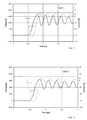
- FIGs 15 to 18 show leakage current measurements and reverse recovery voltage during turn-off for the diodes: Split A, B, C and D.
- the black line (marked by circle with arrow to the left side) shows the voltage, whereas the grey line shows the current (marked by circle with arrow to the right side).
- FIG 15 shows that Split A (low doping concentration at small and high depth) shows a soft turn-off behaviour (3101 V at maximum), but a high leakage current (see also FIG.12 ).
- FIG 16 shows a device with high doping concentration in low and large depth, but the device is snappy and has a high reverse recovery voltage.
- Figs 17 and 18 show the inventive diodes Split C and D, both of which show good properties concerning softness and leakage current so that one of these properties does not scarify the other property.
- the inventive diodes are in particular advantageous for diodes with breakdown voltage above 2.5 kV.
- the inventive diode can advantageously be used as a free-wheeling or clamping diode in IGCT (Integrated gate commutated thyristor) or a free-wheeling diode in the IGBT (insulated gate bipolar transistor) applications.
- IGCT Integrated gate commutated thyristor
- IGBT insulated gate bipolar transistor
- the diode 1 has an (n-) doped drift layer 2 on a cathode side 13 and a p doped anode layer 3 on an anode side 14 opposite to the cathode side 13.
- the anode layer 3 comprises an anode contact layer 5 and an anode buffer layer 4.
- the method comprises the following manufacturing steps in the following order:
- the first and second ions 42, 44 are examplarily chosen to be of the same particle sort.
- the third ions may be of the same particle sort, but also other ions may be used.
- B, Al or Ga ions may be used as first, second and/or third ions 42, 44, 52.
- the first and second ions 42, 44 for the creation of the anode buffer layer 4 can be applied by surface deposition or by ion implantation.
- the ions 42, 44, 52 are deposited only at one side, i.e. the second side 12 (like in the ion implantation method) or on both sides of the wafer (first and second side 11, 12 like in a surface deposition method).
- the ions on the first side 11 are removed before diffusion, e.g.
- the ions are driven-in only at the second side 12 or the ions are diffused on both sides and the wafer is thinned on the first side 11 after diffusion as to completely remove the p doped layer created on the first side 11.
- the first and second ions 42, 44 may be applied in step (b) and (d) with a first and second implant/deposition dose, in the following called implant dose, each of which exemplarily being between 1*10 12 cm -2 and 1*10 13 cm -2 , wherein the sum of the first and second implant dose is exemplarily between 3*10 12 cm -2 and 15*10 12 cm -2 .
- the implant dose of the first ions may be the same as the implant dose for the second ions. However, it may also be advantageous to choose the first implant dose to be lower than the dose of the second ions in order to further improve the softness of the device and to achieve a smaller voltage maximum during turn-off. These effects are achieved, because due to the smaller first implant dose the doping concentration in the third depth (which is mainly responsible for the softness) can be kept low.
- the first ions 42 are at least partly diffused into the wafer 10.
- the first ions 42 are examplarily diffused to a first depth of at least 13 ⁇ m before the second ions 44 are applied.
- the first ions 42 are diffused to a first depth between 13 and 16 ⁇ m, exemplarily between 13 and 15 ⁇ m.
- the first ions 42 are completely diffused before the second ions 44 are applied and diffused.
- the diffusion times for the first and second diffusion may also be adapted due to the desired doping concentration profile.
- FIG 14 the effects are shown for variation of the diffusion times.
- the introduction of a first and second diffusion time corresponds to partly diffusing the first ions 42 before applying the second ions 44.
- the total diffusion time i.e. the sum of the first and second diffusion time is chosen to be so long that at least the first ions 42 are diffused into a fifth depth of 18 to 25 ⁇ m.
- the total diffusion time is the same. The deeper the anode buffer layer is located and the lower the doping profile is at large depths, the better are the switching properties at small currents (see FIG 17 ).
- the upper continuous line in FIG 14 shows the doping profile of a prior art device with one implantation and one diffusion for the anode buffer layer 4 and a diffusion time of 965 min and 1 * 10 13 cm -2 .
- the other profiles have been achieved with the same first and second implant dose of 5 * 10 12 cm -2 , i.e. with the same total ion dose as for the prior art device.
- the total diffusion depth is slightly lower than for longer first diffusion time.
- the first and second ions 42, 44 are diffused in step (e) such that a total doping concentration between 6.0*10 15 and 2.0 * 10 16 cm -3 is achieved in the second depth.
- the fifth depth is the total depth, to which the first ions are diffused to. As the diffusion for the second ions starts later than for the first ions, the second ions are diffused to a shorter depth than the first ions.
- the fifth depth may vary examplarily between 18 to 25 ⁇ m.
- the third ions 52 may be applied in step (f) with a implant dose between 5*10 13 cm -2 and 1*10 15 cm -2 .
- the third ions 52 are diffused such that a maximum doping concentration of the anode contact layer 5 (surface doping concentration) is achieved between 1.0*10 17 cm -3 and 5.0*10 18 cm -3 which ensures a good surge current ability of the device.
- the third ions 52 may be diffused into the wafer 10 up to the fourth depth between 0.5 and 3 ⁇ m. Due to the small depth, into which the third ions 52 are diffused to, the diffusion depth of the first and second ions is mainly given by the first and second diffusion (step (c) and (e)).
- the third diffusion (step (g)) hardly influences the diffusion depth of the first and second ions 42, 44 due to its short diffusion time.
- the anode buffer layer 4 may be made of a plurality of such ion application and afterwards diffusion of these ions.
- Each ion application and diffusion step is performed such that the corresponding ions are partly diffused before the next ions are applied (i.e. step (b) and (c) are repeatedly applied) such that in the end a total doping concentration is achieved between 8.0*10 15 and 2.0 * 10 16 cm -3 in a second depth of 5 ⁇ m, exemplarily between 1.0*10 16 and 2.0 * 10 16 cm -3 and between 1.0*10 14 up to 5.0 * 10 14 cm -3 in a third depth of 15 ⁇ m.
- the implant doses and the diffusion times given at the examples above are lowered proportionally if more implantations and diffusions are performed.
- cathode sided processes on the wafer are performed after finishing the diffusions for the anode layer 3.
- Such a cathode sided process can be the creation of an n-doped cathode layer 25.
- Metal layers for the cathode and anode electrode 6, 7 are typically deposited on the cathode and anode side 21, 22 after finalizing all layers in the wafer 10.
- a metal layer as a cathode electrode 6 is arranged on top of the cathode layer 25 or on top of the drift layer 2, respectively, for a device without a cathode layer 25.
- a metal layer as an anode electrode 7 is arranged on the anode side 14 of the wafer.
- a defect layer 8 may be created in a sixth depth within the anode buffer layer by irradiation.
- the defect layer 8 may be created at any manufacturing stage, even after the creation of the metal layers as electrodes 6, 7.
- Light ions such as protons or helium or protons, electrons or heavy metal diffusion are exemplarily used for the creation of the defect layer 6.
- the irradiation energy of these ions is chosen such that a defect layer 6 is created with a defect peak, which is arranged in a depth beyond the anode contact layer and outside the space charge region so that the leakage current is not increased, which is exemplarily 8 ⁇ m, in particular 7 ⁇ m. Therefore, the defect layer is created in a sixth depth of at most 8 ⁇ m, exemplarily between 5 and 7 ⁇ m.
- the defect layer By placing the defect layer between the crossing point of the anode buffer and anode contact layer, the doping concentration is comparatively low and therefore, the electron-hole plasma in the on-state can be significantly reduced. This improves the SOA of the diode and soft recovery can be achieved. Due to the slower drop of the doping concentration in the anode buffer layer than in the anode contact layer, the process is less delicate to effects, which influence the depth of the defect layer (like changes of the irradiation energy or to any coarseness of the surface of the wafer). At the same time, the defect layer is placed into a region which is not reached by the space charge region (SCR) of the anode junction at breakdown voltage. Thereby, the leakage current can be kept low.
- SCR space charge region
- the radiation defects do not increase the leakage current, because they are not present at the SCR.
- Local lifetime control can be achieved due to the presence of the defect centers without enhancing the leakage current. Thereby, the diode can be operated at higher temperatures.
- the inventive diode may optionally have edge terminations known from prior art like positive bevels, which means that the diode 1 has a smaller width at the cathode side 13 than at the anode side 14, or negative bevels as shown in FIG 20 , which means that the diode 1 has a larger width at the cathode side 13 than at the anode side 14.
- the width of the device is the distance between the lateral sides of the device, whereas the lateral sides are the sides between the cathode side and the anode side 13, 14.
- the diode 1 can also be terminated by guard rings or VLD (Variation of Lateral Doping).
- the angle measured from the cathode side inside the silicon is larger than 90°
- the angle measured inside the silicon is larger than 90° when measured at the anode side.
- the electric field can be reduced on the bevel over a great length due a small doping concentration gradient, which gives advantages in the increased static blocking for the device. This effect is further enhanced by the inventive doping profile.
- the advantages of the bevel termination is the easy manufacturing of discrete diodes and lower leakage current compared to the guard rings and VLD.
Landscapes
- Electrodes Of Semiconductors (AREA)
- Thyristors (AREA)
Abstract
Description
- The invention relates to the field of power electronics and more particularly to a method for manufacturing a bipolar diode according to
claim 1 and to such a bipolar diode according to the preamble ofclaim 14. - A prior art diode comprises on a cathode side an (n-) doped drift layer and on an anode side opposite to the cathode side a p doped anode layer. On top of the p doped anode layer a metal layer which functions as an anode electrode is arranged. On the cathode side, a higher (n+) doped cathode layer is arranged. A metal layer in form of a cathode electrode is arranged on top of the (n+) doped cathode layer.
- Such devices are created by making one ion diffusion for the anode contact layer and another one for the anode buffer layer, by which method first ions for the anode buffer layer are implanted and deeply diffused into a wafer into a depth of around 20 µm and afterwards, second ions are implanted and diffused into a depth of around 5 µm.
-
FIG 11 shows the doping profiles of prior art p doped anode layers (split A and B), which comprise a highly doped and shallow anode contact layer and a deeper diffused, but lower doped anode buffer layer. The maximum doping concentration of the anode contact layer is around 5 * 1018 cm-3. - The anode buffer layer can be optimized either for leakage current, for which a high doping concentration is needed in a low depth of 5 µm, i.e. a doping concentration higher than 1*1016 cm-3 in 5 µm depth is used for such devices (Split A). Such a high doping concentration in 5 µm has the consequence that the doping concentration in a larger depth of 15 µm is also as high as 7.2 * 1014 cm-3. This is the consequence from using a single diffusion for the anode buffer layer. However, the high doping concentration in 15 µm has disadvantages for the soft turn off of the device.
- Therefore, other devices are made, which are optimized for soft turn off of the device, which requires a deep, but low doped anode buffer layer, which is achieved by having a low doping concentration of 1.5 * 1014 cm-3 in 15 µm depth (Split B). However, this can only be achieved by also lowering the doping concentration in 5 µm to 4 * 1015 cm-3, which value is again unfavourable for the leakage current.
- With such prior art devices, it is not possible to influence the curvature of the doping concentration profile, and thus, it is not possible to optimize leakage current and softness simultaneously in one device.
- It is an object of the invention to provide a method for manufacturing a bipolar diode having better softness and less leakage current, than achievable by prior art methods.
- This object is achieved by a method for manufacturing a bipolar diode according to
claim 1 and by a bipolar diode according toclaim 14. - An inventive method for manufacturing a bipolar diode having a drift layer of a first conductivity type on a cathode side and an anode layer of a second conductivity type on an anode side opposite to the cathode side is provided, wherein the second conductivity type is different from the first conductivity type. The anode layer comprises an anode contact layer and an anode buffer layer. The method comprises the following manufacturing steps in the following order:
- (a) providing a low-doped wafer of the first conductivity type, which wafer has a first side and a second side opposite to the first side, wherein such part of the wafer of unamended doping concentration in the finalized diode forms the drift layer,
- (b) applying first ions to the wafer on the second side,
- (c) diffusing the first ions into the wafer up to a first depth,
- (d) applying second ions to the wafer on the second side,
- (e) creating the anode buffer layer by diffusing the first and second ions into the wafer such that a total doping concentration is achieved between 8.0*1015 and 2.0 * 1016 cm-3 in a second depth of 5 µm and between 1.0*1014 up to 5.0 * 1014 cm-3 in a third depth of 15 µm,
- (f) applying third ions to the wafer on the second side, and
- (g) creating an anode contact layer by diffusing the third ions into the wafer up to a fourth depth of at most 5 µm,
- All depths are measured from the second side.
- By applying a triple anode layer made of an anode contact layer and at least a double diffused anode buffer layer the doping concentration profile can be enhanced in a shallow depth of 5 µm and still can be made deep and lowly diffused in 15 µm. Thus, the inventive devices provide in terms of device performance lower leakage currents and softer turn-off behavior.
- The doping concentration profiles shown in
FIG 11 have been achieved with the following doses:Split A Split B Split C Split D first ion dose 5*1012 cm -215*1012 cm - 25*1012 cm -25*1012 cm-2 second ion dose --- --- 1*1013 cm -25*1012 cm-2 third ion dose 5*1014 cm -25*1014 cm -25*1014 cm -25*1014 cm-2 Vrmax during reverse recovery (diode turn-off) 3101 V 4720 V 3434 V 3225 V I reverse Mean Leakage current 1 mA 0.78 A 0.79 A 0.88 A -
FIG 13 shows the doping concentration profiles ofFIG 11 in more detail for the smaller depths. Also schematically shown is the electric field during blocking. If the electric field comes too close to the second side it penetrates into the zone of irradiation defects (depth of 5 to 7 um - not shown in the graph) generating higher leakage current. Therefore, Split A, for which the space charge region extends to a small depth (from the second side) has the largest leakage current of the devices. Prior art Split B and the inventive Split C show about the same low leakage current, whereas Split D has a slightly higher leakage current, but still close to those of Split B and C. This result is also confirmed byFIG 12 , in which the probability of having a diode with a given leakage current is shown. Split A is in the graphics far on the right side, i.e. on the side of high leakage current, whereas Split B, C and D have much lower leakage current. - The
Figs 15 to 18 show leakage current measurements and reverse recovery voltage during turn-off for the diodes: Split A, B, C and D. In the figures the black line (marked by circle with arrow to the left side) shows the voltage, whereas the grey line shows the current (marked by circle with arrow to the right side).FIG 15 shows that Split A (low doping concentration at small and high depth) shows a soft turn-off behaviour (3101 V at maximum), but a high leakage current (see alsoFIG.12 ). - On the other hand,
FIG 16 shows a device with high doping concentration in low and large depth, but the device is snappy and has a high reverse recovery voltage. The nextFigs 17 and 18 show the inventive diodes Split C and D, both of which show good properties concerning softness and leakage current so that one of these properties does not scarify the other property. - The inventive diodes are in particular advantageous for diodes with breakdown voltage above 2.5 kV.
- The inventive diode can advantageously be used as a free-wheeling or clamping diode in IGCT (Integrated gate commutated thyristor) or a free-wheeling diode in the IGBT (insulated gate bipolar transistor) applications.
- Further preferred embodiments of the inventive subject matter are disclosed in the dependent claims.
- The subject matter of the invention will be explained in more detail in the following text with reference to the attached drawings, in which:
- FIGs 1 to
- 7 show manufacturing steps for manufacturing an inventive semiconductor device;
- FIG 8
- shows a cross sectional view on an inventive diode;
- FIG 9
- shows a cross sectional view on an inventive diode having a defect layer;
- FIG 10
- shows a cross sectional view on an inventive diode having a cathode layer;
- FIG 11
- shows doping concentration profiles of inventive diodes and prior art diodes;
- FIG 12
- shows probability curves of having a diode type with a given leakage current;
- FIG 13
- shows the doping profiles of the diodes according to
FIG 11 in more detail; - FIG 14
- shows doping concentration profiles of inventive diodes and prior art diodes, wherein the diffusions have been performed with different diffusion times;
- FIG 15-18
- show leakage current and reverse recovery voltage versus time for inventive diodes and prior art diodes;
- FIG 19
- shows edge termination of another diode according to the invention; and
- FIG 20
- shows edge termination of another diode according to the invention.
- The reference symbols used in the figures and their meaning are summarized in the list of reference symbols. Generally, alike or alike-functioning parts are given the same reference symbols. The described embodiments are meant as examples and shall not confine the invention.
- In the
FIGs 1 to 8 a method for manufacturing an inventivebipolar diode 1 is shown. Thediode 1 has an (n-)doped drift layer 2 on acathode side 13 and a p dopedanode layer 3 on ananode side 14 opposite to thecathode side 13. Theanode layer 3 comprises ananode contact layer 5 and ananode buffer layer 4. - The method comprises the following manufacturing steps in the following order:
- (a) providing a low-(n-) doped
wafer 10, whichwafer 10 has a first side 11 (cathode side 13) and a second side 12 (anode side 14) opposite to the first side 11 (FIG 1 ), wherein such part of the wafer of unamended doping concentration in the finalized diode forms thedrift layer 2, - (b) applying
first ions 42 to thewafer 10 on the second side 12 (FIG 2 ) for the creation of the p dopedanode buffer layer 4, - (c) diffusing the
first ions 42 into thewafer 10 up to a first depth (FIG 3 ), examplarily to at least 13 µm, - (d) applying
second ions 44 to thewafer 10 on the second side 12 (FIG 4 ) for the creation of the p dopedanode buffer layer 4, - (e) creating the
anode buffer layer 4 by diffusing the first andsecond ions wafer 10 such that a total doping concentration is achieved between 8.0*1015 and 2.0 * 1016 cm-3 in a second depth of 5 µm and between 1.0*1014 up to 5.0 * 1014 cm-3 in a third depth of 15 µm (FIG 5 ), - (f) applying
third ions 52 to thewafer 10 on the second side 12 (FIG 6 ) for the creation of theanode contact layer 5, and - (g) creating an
anode contact layer 5 by diffusing thethird ions 52 into thewafer 10 up to a fourth depth of at most 5 µm (FIG 7 ),
wherein all depths are measured from thesecond side 12, i.e. from the anode sided surface of theanode contact layer 5. - In step (b) and (d) the first and
second ions third ions - The first and
second ions third ions 52 for the creation of the anode contact layer 5) can be applied by surface deposition or by ion implantation. Depending of the method for applying the ions onto the wafer surface, theions second side first side 11 are removed before diffusion, e.g. by etching or polishing, and then the ions are driven-in only at thesecond side 12 or the ions are diffused on both sides and the wafer is thinned on thefirst side 11 after diffusion as to completely remove the p doped layer created on thefirst side 11. - The first and
second ions - The implant dose of the first ions may be the same as the implant dose for the second ions. However, it may also be advantageous to choose the first implant dose to be lower than the dose of the second ions in order to further improve the softness of the device and to achieve a smaller voltage maximum during turn-off. These effects are achieved, because due to the smaller first implant dose the doping concentration in the third depth (which is mainly responsible for the softness) can be kept low.
- In step (c) the
first ions 42 are at least partly diffused into thewafer 10. Depending on the desired doping concentration profile, thefirst ions 42 are examplarily diffused to a first depth of at least 13 µm before thesecond ions 44 are applied. In another embodiment thefirst ions 42 are diffused to a first depth between 13 and 16 µm, exemplarily between 13 and 15 µm. In another alternative, thefirst ions 42 are completely diffused before thesecond ions 44 are applied and diffused. By this at least partial first diffusion, the resulting doping concentration profile is risen in shallower depths and reduced in deeper depths as shown inFIG 14 , which figure is explained in more detail below. - The diffusion times for the first and second diffusion may also be adapted due to the desired doping concentration profile. In
FIG 14 the effects are shown for variation of the diffusion times. The introduction of a first and second diffusion time corresponds to partly diffusing thefirst ions 42 before applying thesecond ions 44. The total diffusion time, i.e. the sum of the first and second diffusion time is chosen to be so long that at least thefirst ions 42 are diffused into a fifth depth of 18 to 25 µm. For all curves given inFIG 14 , the total diffusion time is the same. The deeper the anode buffer layer is located and the lower the doping profile is at large depths, the better are the switching properties at small currents (seeFIG 17 ). The upper continuous line inFIG 14 shows the doping profile of a prior art device with one implantation and one diffusion for theanode buffer layer 4 and a diffusion time of 965 min and 1 * 1013 cm-2. The other profiles have been achieved with the same first and second implant dose of 5 * 1012 cm-2, i.e. with the same total ion dose as for the prior art device. The shorter the first diffusion time (first time given in the legend ofFIG 14 ) is compared to the second diffusion time (second time given in the legend ofFIG 14 ), the higher the doping concentration in all depths, the leakage current is lowered (upper profiles inFIG 14 ). The longer the first diffusion time is, i.e. the deeper the ions have been driven-in in the first diffusion, the lower is the doping profile in all depths, i.e. the softness is further improved (lower profile inFIG 14 ). The total diffusion depth is slightly lower than for longer first diffusion time. - In an exemplary embodiment, the first and
second ions - The fifth depth is the total depth, to which the first ions are diffused to. As the diffusion for the second ions starts later than for the first ions, the second ions are diffused to a shorter depth than the first ions. The fifth depth may vary examplarily between 18 to 25 µm.
- The
third ions 52 may be applied in step (f) with a implant dose between 5*1013 cm-2 and 1*1015 cm-2. Examplarily, in step (g) thethird ions 52 are diffused such that a maximum doping concentration of the anode contact layer 5 (surface doping concentration) is achieved between 1.0*1017 cm-3 and 5.0*1018 cm-3 which ensures a good surge current ability of the device. Thethird ions 52 may be diffused into thewafer 10 up to the fourth depth between 0.5 and 3 µm. Due to the small depth, into which thethird ions 52 are diffused to, the diffusion depth of the first and second ions is mainly given by the first and second diffusion (step (c) and (e)). The third diffusion (step (g)) hardly influences the diffusion depth of the first andsecond ions - Alternatively to a diode having an
anode buffer layer 4 made of two diffusion steps (c) and (e)), theanode buffer layer 4 may be made of a plurality of such ion application and afterwards diffusion of these ions. Each ion application and diffusion step is performed such that the corresponding ions are partly diffused before the next ions are applied (i.e. step (b) and (c) are repeatedly applied) such that in the end a total doping concentration is achieved between 8.0*1015 and 2.0 * 1016 cm-3 in a second depth of 5 µm, exemplarily between 1.0*1016 and 2.0 * 1016 cm-3 and between 1.0*1014 up to 5.0 * 1014 cm-3 in a third depth of 15 µm. Of course, the implant doses and the diffusion times given at the examples above are lowered proportionally if more implantations and diffusions are performed. - Examplarily, cathode sided processes on the wafer are performed after finishing the diffusions for the
anode layer 3. Such a cathode sided process can be the creation of an n-dopedcathode layer 25. - Metal layers for the cathode and
anode electrode wafer 10. A metal layer as acathode electrode 6 is arranged on top of thecathode layer 25 or on top of thedrift layer 2, respectively, for a device without acathode layer 25. A metal layer as ananode electrode 7 is arranged on theanode side 14 of the wafer. - Additionally to the creation of the
inventive anode layer 3, a defect layer 8 may be created in a sixth depth within the anode buffer layer by irradiation. The defect layer 8 may be created at any manufacturing stage, even after the creation of the metal layers aselectrodes defect layer 6. The irradiation energy of these ions is chosen such that adefect layer 6 is created with a defect peak, which is arranged in a depth beyond the anode contact layer and outside the space charge region so that the leakage current is not increased, which is exemplarily 8 µm, in particular 7 µm. Therefore, the defect layer is created in a sixth depth of at most 8 µm, exemplarily between 5 and 7 µm. - By placing the defect layer between the crossing point of the anode buffer and anode contact layer, the doping concentration is comparatively low and therefore, the electron-hole plasma in the on-state can be significantly reduced. This improves the SOA of the diode and soft recovery can be achieved. Due to the slower drop of the doping concentration in the anode buffer layer than in the anode contact layer, the process is less delicate to effects, which influence the depth of the defect layer (like changes of the irradiation energy or to any coarseness of the surface of the wafer). At the same time, the defect layer is placed into a region which is not reached by the space charge region (SCR) of the anode junction at breakdown voltage. Thereby, the leakage current can be kept low. By keeping the peak of the defect centers at a smaller depth than the depth of the SCR the radiation defects do not increase the leakage current, because they are not present at the SCR. Local lifetime control can be achieved due to the presence of the defect centers without enhancing the leakage current. Thereby, the diode can be operated at higher temperatures.
- As shown in
FIG 19 , the inventive diode may optionally have edge terminations known from prior art like positive bevels, which means that thediode 1 has a smaller width at thecathode side 13 than at theanode side 14, or negative bevels as shown inFIG 20 , which means that thediode 1 has a larger width at thecathode side 13 than at theanode side 14. The width of the device is the distance between the lateral sides of the device, whereas the lateral sides are the sides between the cathode side and theanode side diode 1 can also be terminated by guard rings or VLD (Variation of Lateral Doping). - For devices with a positive or negative bevel, there is an angle of the lateral side of a wafer, which side is arranged between the cathode and the anode side, which angle is different from 90°. In case of a positive bevel, the angle measured from the cathode side inside the silicon is larger than 90°, for a negative bevel, the angle measured inside the silicon is larger than 90° when measured at the anode side. With a negative bevel, the electric field can be reduced on the bevel over a great length due a small doping concentration gradient, which gives advantages in the increased static blocking for the device. This effect is further enhanced by the inventive doping profile. The advantages of the bevel termination is the easy manufacturing of discrete diodes and lower leakage current compared to the guard rings and VLD.
-
- 1
- diode
- 10
- wafer
- 11
- first side
- 12
- second side
- 13
- cathode side
- 14
- anode side
- 2
- drift layer
- 25
- cathode layer
- 3
- anode layer
- 4
- anode buffer layer
- 42
- first ions
- 44
- Second ions
- 5
- anode contact layer
- 52
- third ions
- 6
- cathode electrode
- 7
- anode electrode
- 8
- defect layer
Claims (15)
- Method for manufacturing a bipolar diode (1) having a drift layer (2) of a first conductivity type on a cathode side (13) and an anode layer (3) of a second conductivity type on an anode side (14) opposite to the cathode side (13), which anode layer (3) comprises an anode contact layer (5) and an anode buffer layer (4), wherein the second conductivity type is different from the first conductivity type, the method comprising the following manufacturing steps in the following order:(a) providing a low-doped wafer (10) of the first conductivity type, which wafer (10) has a first side (11) and a second side (12) opposite to the first side (11), wherein such part of the wafer of unamended doping concentration in the finalized diode forms the drift layer (2),(b) applying first ions (42) to the wafer (10) on the second side (12),(c) diffusing the first ions (42) into the wafer (10) up to a first depth,(d) applying second ions (44) to the wafer (10) on the second side (12),(e) creating the anode buffer layer (4) by diffusing the first and second ions (42, 44) into the wafer (10) such that a total doping concentration is achieved between 8.0*1015 and 2.0 * 1016 cm-3 in a second depth of 5 µm and between 1.0*1014 up to 5.0 * 1014 cm-3 in a third depth of 15 µm,(f) applying third ions (52) to the wafer (10) on the second side (12), and(g) creating the anode contact layer (5) by diffusing the third ions (52) into the wafer (10) up to a fourth depth of at most 5 µm,
wherein all depths are measured from the second side (12). - Method according to claim 1, comprising
diffusing the first ions (42) in step (c) up to a first depth of at least 13 µm. - Method according to claim 1 or 2, comprising
diffusing the third ions (52) in step (g) such that a maximum doping concentration of the anode contact layer (5) between 1.0*1017 cm-3 and 5.0*1018cm-3 achieved. - Method according to any of the claims 1 to 3, comprising diffusing the third ions (52) in step (g) into the wafer (10) up to a fourth depth between 0.5 and 3 µm.
- Method according to any of the claims 1 to 4, comprising diffusing the first and second ions (42, 44) in step (e) such that a total doping concentration between 1.0*1016 and 2.0 * 1016 cm-3 is achieved in the second depth.
- Method according to any of the claims 1 to 5, comprising diffusing the first ions (42) in step (e) into the wafer (10) up to a fifth depth between 18 and 25 µm.
- Method according to any of the claims 1 to 6, comprising creating a defect layer (9) by irradiation in a sixth depth of at most 8 µm.
- Method according to any of the claims 1 to 7, comprising creating a defect layer (9) by irradiation in a sixth depth between 5 and 7 µm.
- Method according to any of the claims 1 to 8, comprising applying the first and second ions (42, 44) in step (b) and (d) with a first and second implant dose, wherein the sum of the first and second implant dose is between 3*1012cm-2 and 15*1012cm-2.
- Method according to any of the claims 1 to 9, comprising applying the first and second ions (42, 44) in step (b) and (d) with a first and second implant dose, wherein the implant dose of the first ions is lower than the implant dose of the second ions.
- Method according to any of the claims 1 to 10, comprising diffusing the first ions (42) in step (c) for a first diffusion time and
diffusing the first and second ions (42, 44) in step (e) for a second diffusion time,
wherein the first diffusion time is longer than the second diffusion time. - Method according to any of the claims 1 to 11, comprising applying the same ions as first and second ions (42, 44), in particular applying B, Al or Ga ions as first and second ions (42, 44).
- Method according to any of the claims 1 to 12, comprising the first depth in step (c) being at most 16 µm, in particular at most 15 µm.
- Bipolar diode (1) having a drift layer (2) of a first conductivity type on a cathode side (13) and an anode layer (3) of a second conductivity type on an anode side (14), which second conductivity type is different from the first conductivity type, the cathode side (13) being opposite to the anode side (14), wherein the anode layer (3) comprises a diffused anode contact layer (5) and a diffused anode buffer layer (4),
wherein the anode contact layer (5) is arranged up to a depth of at most 5 µm, characterized in, that the anode buffer layer (4) has a doping concentration between 8.0*1015 and 2.0 * 1016 cm-3 in a depth of 5 µm and
between 1.0*1014 up to 5.0 * 1014 cm-3 in a depth of 15 µm,
wherein all depths are measured from the anode side (14). - Diode according to claim 14, characterized in, that the anode buffer layer (4) is arranged in a depth up to between 18 and 25 µm.
Priority Applications (5)
| Application Number | Priority Date | Filing Date | Title |
|---|---|---|---|
| EP11169792.6A EP2535940B1 (en) | 2011-06-14 | 2011-06-14 | Bipolar diode and method for manufacturing the same |
| KR1020120063300A KR101710220B1 (en) | 2011-06-14 | 2012-06-13 | Bipolar punch-through semiconductor device and method for manufacturing such a semiconductor device |
| US13/523,184 US8525302B2 (en) | 2011-06-14 | 2012-06-14 | Bipolar punch-through semiconductor device and method for manufacturing such a semiconductor device |
| JP2012134819A JP5992216B2 (en) | 2011-06-14 | 2012-06-14 | Bipolar punch-through semiconductor device and method for manufacturing such a semiconductor device |
| CN201210273480.XA CN102832122B (en) | 2011-06-14 | 2012-06-14 | Bipolar punch-through semiconductor device and the manufacture method of this semiconductor device |
Applications Claiming Priority (1)
| Application Number | Priority Date | Filing Date | Title |
|---|---|---|---|
| EP11169792.6A EP2535940B1 (en) | 2011-06-14 | 2011-06-14 | Bipolar diode and method for manufacturing the same |
Publications (2)
| Publication Number | Publication Date |
|---|---|
| EP2535940A1 true EP2535940A1 (en) | 2012-12-19 |
| EP2535940B1 EP2535940B1 (en) | 2013-08-21 |
Family
ID=44721633
Family Applications (1)
| Application Number | Title | Priority Date | Filing Date |
|---|---|---|---|
| EP11169792.6A Active EP2535940B1 (en) | 2011-06-14 | 2011-06-14 | Bipolar diode and method for manufacturing the same |
Country Status (5)
| Country | Link |
|---|---|
| US (1) | US8525302B2 (en) |
| EP (1) | EP2535940B1 (en) |
| JP (1) | JP5992216B2 (en) |
| KR (1) | KR101710220B1 (en) |
| CN (1) | CN102832122B (en) |
Cited By (3)
| Publication number | Priority date | Publication date | Assignee | Title |
|---|---|---|---|---|
| WO2014202750A1 (en) * | 2013-06-20 | 2014-12-24 | Abb Technology Ag | Fast recovery diode |
| EP3196943A1 (en) | 2016-01-22 | 2017-07-26 | ABB Technology AG | Bipolar diode and method for manufacturing such a diode |
| US10847626B2 (en) | 2017-12-21 | 2020-11-24 | 3-5 Power Electronics GmbH | Stacked III-V semiconductor component |
Families Citing this family (2)
| Publication number | Priority date | Publication date | Assignee | Title |
|---|---|---|---|---|
| DE102017002936A1 (en) * | 2017-03-24 | 2018-09-27 | 3-5 Power Electronics GmbH | III-V semiconductor diode |
| CN113745315B (en) * | 2021-07-28 | 2023-11-14 | 西安电子科技大学 | P-type base silicon carbide DAS device and preparation method thereof |
Citations (1)
| Publication number | Priority date | Publication date | Assignee | Title |
|---|---|---|---|---|
| DE102007001108A1 (en) * | 2007-01-04 | 2008-07-10 | Infineon Technologies Ag | diode |
Family Cites Families (11)
| Publication number | Priority date | Publication date | Assignee | Title |
|---|---|---|---|---|
| US4106953A (en) * | 1976-12-28 | 1978-08-15 | Motorola, Inc. | Method of producing an ion implanted tuning diode |
| US5960275A (en) * | 1996-10-28 | 1999-09-28 | Magemos Corporation | Power MOSFET fabrication process to achieve enhanced ruggedness, cost savings, and product reliability |
| JPH10294448A (en) * | 1997-04-22 | 1998-11-04 | Hitachi Ltd | Manufacturing method of high voltage semiconductor device |
| GB9804177D0 (en) * | 1998-02-28 | 1998-04-22 | Philips Electronics Nv | Semiconductor switch devices and their manufacture |
| US20030087510A1 (en) * | 2001-11-06 | 2003-05-08 | Chen Aikwo Eric | Method of forming MOS transistor graded junctions using multiple implant of low diffusion specie, and a device formed thereby |
| JP4367508B2 (en) * | 2007-03-13 | 2009-11-18 | 株式会社デンソー | Silicon carbide semiconductor device and manufacturing method thereof |
| DE102008049664B3 (en) * | 2008-09-30 | 2010-02-11 | Infineon Technologies Austria Ag | Method for producing semiconductor body of diode, involves forming n-conductive zone by implantation of protons in direction in semiconductor body in depth and by heating body for forming hydrogen-reduced donors |
| KR20110094066A (en) * | 2008-12-15 | 2011-08-19 | 에이비비 테크놀로지 아게 | Bipolar Punch-Through Semiconductor Devices and Methods of Manufacturing Such Semiconductor Devices |
| JP5569532B2 (en) * | 2009-11-02 | 2014-08-13 | 富士電機株式会社 | Semiconductor device and manufacturing method of semiconductor device |
| EP2320452B1 (en) * | 2009-11-09 | 2011-10-19 | ABB Technology AG | Fast recovery diode and its manufacturing method |
| EP2320451B1 (en) * | 2009-11-09 | 2013-02-13 | ABB Technology AG | Fast recovery Diode |
-
2011
- 2011-06-14 EP EP11169792.6A patent/EP2535940B1/en active Active
-
2012
- 2012-06-13 KR KR1020120063300A patent/KR101710220B1/en active Active
- 2012-06-14 US US13/523,184 patent/US8525302B2/en active Active
- 2012-06-14 JP JP2012134819A patent/JP5992216B2/en active Active
- 2012-06-14 CN CN201210273480.XA patent/CN102832122B/en active Active
Patent Citations (1)
| Publication number | Priority date | Publication date | Assignee | Title |
|---|---|---|---|---|
| DE102007001108A1 (en) * | 2007-01-04 | 2008-07-10 | Infineon Technologies Ag | diode |
Non-Patent Citations (2)
| Title |
|---|
| VOBECKI J ET AL: "The Radiation Enhanced Diffusion (RED) Diode realization of a large area p+p-n-n+ structure with high SOA", 2009 21ST INTERNATIONAL SYMPOSIUM ON POWER SEMICONDUCTOR DEVICES & IC'S (ISPSD) - 14-18 JUNE 2009 - BARCELONA, SPAIN, IEEE, PISCATAWAY, NJ, USA, 14 June 2009 (2009-06-14), pages 144 - 147, XP031485159, ISBN: 978-1-4244-3525-8 * |
| VOBECKY J ET AL: "Helium irradiated high-power P-i-N diode with low ON-state voltage drop", SOLID STATE ELECTRONICS, ELSEVIER SCIENCE PUBLISHERS, BARKING, GB, vol. 47, no. 1, 1 January 2003 (2003-01-01), pages 45 - 50, XP004392865, ISSN: 0038-1101, DOI: 10.1016/S0038-1101(02)00250-2 * |
Cited By (3)
| Publication number | Priority date | Publication date | Assignee | Title |
|---|---|---|---|---|
| WO2014202750A1 (en) * | 2013-06-20 | 2014-12-24 | Abb Technology Ag | Fast recovery diode |
| EP3196943A1 (en) | 2016-01-22 | 2017-07-26 | ABB Technology AG | Bipolar diode and method for manufacturing such a diode |
| US10847626B2 (en) | 2017-12-21 | 2020-11-24 | 3-5 Power Electronics GmbH | Stacked III-V semiconductor component |
Also Published As
| Publication number | Publication date |
|---|---|
| US20120319227A1 (en) | 2012-12-20 |
| KR20120138689A (en) | 2012-12-26 |
| KR101710220B1 (en) | 2017-02-24 |
| JP5992216B2 (en) | 2016-09-14 |
| EP2535940B1 (en) | 2013-08-21 |
| US8525302B2 (en) | 2013-09-03 |
| CN102832122A (en) | 2012-12-19 |
| CN102832122B (en) | 2016-08-03 |
| JP2013004982A (en) | 2013-01-07 |
Similar Documents
| Publication | Publication Date | Title |
|---|---|---|
| EP2320451B1 (en) | Fast recovery Diode | |
| EP2320452B1 (en) | Fast recovery diode and its manufacturing method | |
| KR101745437B1 (en) | Bipolar non-punch-through power semiconductor device | |
| CN101159285A (en) | Semiconductor device and manufacturing method thereof | |
| US9673308B2 (en) | Semiconductor device manufacturing method | |
| EP2535940B1 (en) | Bipolar diode and method for manufacturing the same | |
| KR20150066596A (en) | Semiconductor device | |
| EP2463913A1 (en) | Bipolar reverse-blocking non-punch-through power semiconductor device | |
| WO2014202750A1 (en) | Fast recovery diode | |
| JP6665713B2 (en) | Semiconductor device | |
| EP3196943A1 (en) | Bipolar diode and method for manufacturing such a diode | |
| US11024502B2 (en) | Semiconductor devices and methods for forming semiconductor devices | |
| US10069000B2 (en) | Bipolar non-punch-through power semiconductor device | |
| WO2009077566A1 (en) | Power semiconductor device and method for manufacturing such a device | |
| CN118630067A (en) | Fast recovery diode and method for manufacturing a fast recovery diode |
Legal Events
| Date | Code | Title | Description |
|---|---|---|---|
| PUAI | Public reference made under article 153(3) epc to a published international application that has entered the european phase |
Free format text: ORIGINAL CODE: 0009012 |
|
| 17P | Request for examination filed |
Effective date: 20120608 |
|
| AK | Designated contracting states |
Kind code of ref document: A1 Designated state(s): AL AT BE BG CH CY CZ DE DK EE ES FI FR GB GR HR HU IE IS IT LI LT LU LV MC MK MT NL NO PL PT RO RS SE SI SK SM TR |
|
| AX | Request for extension of the european patent |
Extension state: BA ME |
|
| GRAP | Despatch of communication of intention to grant a patent |
Free format text: ORIGINAL CODE: EPIDOSNIGR1 |
|
| RIC1 | Information provided on ipc code assigned before grant |
Ipc: H01L 29/861 20060101AFI20130321BHEP Ipc: H01L 29/36 20060101ALI20130321BHEP Ipc: H01L 29/06 20060101ALN20130321BHEP Ipc: H01L 29/32 20060101ALN20130321BHEP Ipc: H01L 21/329 20060101ALI20130321BHEP |
|
| RIC1 | Information provided on ipc code assigned before grant |
Ipc: H01L 29/06 20060101ALN20130403BHEP Ipc: H01L 21/329 20060101ALI20130403BHEP Ipc: H01L 29/32 20060101ALN20130403BHEP Ipc: H01L 29/861 20060101AFI20130403BHEP Ipc: H01L 29/36 20060101ALI20130403BHEP |
|
| INTG | Intention to grant announced |
Effective date: 20130422 |
|
| GRAS | Grant fee paid |
Free format text: ORIGINAL CODE: EPIDOSNIGR3 |
|
| GRAA | (expected) grant |
Free format text: ORIGINAL CODE: 0009210 |
|
| AK | Designated contracting states |
Kind code of ref document: B1 Designated state(s): AL AT BE BG CH CY CZ DE DK EE ES FI FR GB GR HR HU IE IS IT LI LT LU LV MC MK MT NL NO PL PT RO RS SE SI SK SM TR |
|
| REG | Reference to a national code |
Ref country code: GB Ref legal event code: FG4D |
|
| REG | Reference to a national code |
Ref country code: CH Ref legal event code: EP |
|
| REG | Reference to a national code |
Ref country code: AT Ref legal event code: REF Ref document number: 628536 Country of ref document: AT Kind code of ref document: T Effective date: 20130915 |
|
| REG | Reference to a national code |
Ref country code: IE Ref legal event code: FG4D |
|
| REG | Reference to a national code |
Ref country code: DE Ref legal event code: R096 Ref document number: 602011002665 Country of ref document: DE Effective date: 20131017 |
|
| REG | Reference to a national code |
Ref country code: NL Ref legal event code: VDEP Effective date: 20130821 Ref country code: AT Ref legal event code: MK05 Ref document number: 628536 Country of ref document: AT Kind code of ref document: T Effective date: 20130821 |
|
| REG | Reference to a national code |
Ref country code: LT Ref legal event code: MG4D |
|
| PG25 | Lapsed in a contracting state [announced via postgrant information from national office to epo] |
Ref country code: IS Free format text: LAPSE BECAUSE OF FAILURE TO SUBMIT A TRANSLATION OF THE DESCRIPTION OR TO PAY THE FEE WITHIN THE PRESCRIBED TIME-LIMIT Effective date: 20131221 Ref country code: NO Free format text: LAPSE BECAUSE OF FAILURE TO SUBMIT A TRANSLATION OF THE DESCRIPTION OR TO PAY THE FEE WITHIN THE PRESCRIBED TIME-LIMIT Effective date: 20131121 Ref country code: HR Free format text: LAPSE BECAUSE OF FAILURE TO SUBMIT A TRANSLATION OF THE DESCRIPTION OR TO PAY THE FEE WITHIN THE PRESCRIBED TIME-LIMIT Effective date: 20130821 Ref country code: CY Free format text: LAPSE BECAUSE OF FAILURE TO SUBMIT A TRANSLATION OF THE DESCRIPTION OR TO PAY THE FEE WITHIN THE PRESCRIBED TIME-LIMIT Effective date: 20130918 Ref country code: SE Free format text: LAPSE BECAUSE OF FAILURE TO SUBMIT A TRANSLATION OF THE DESCRIPTION OR TO PAY THE FEE WITHIN THE PRESCRIBED TIME-LIMIT Effective date: 20130821 Ref country code: PT Free format text: LAPSE BECAUSE OF FAILURE TO SUBMIT A TRANSLATION OF THE DESCRIPTION OR TO PAY THE FEE WITHIN THE PRESCRIBED TIME-LIMIT Effective date: 20131223 Ref country code: LT Free format text: LAPSE BECAUSE OF FAILURE TO SUBMIT A TRANSLATION OF THE DESCRIPTION OR TO PAY THE FEE WITHIN THE PRESCRIBED TIME-LIMIT Effective date: 20130821 Ref country code: AT Free format text: LAPSE BECAUSE OF FAILURE TO SUBMIT A TRANSLATION OF THE DESCRIPTION OR TO PAY THE FEE WITHIN THE PRESCRIBED TIME-LIMIT Effective date: 20130821 |
|
| PG25 | Lapsed in a contracting state [announced via postgrant information from national office to epo] |
Ref country code: GR Free format text: LAPSE BECAUSE OF FAILURE TO SUBMIT A TRANSLATION OF THE DESCRIPTION OR TO PAY THE FEE WITHIN THE PRESCRIBED TIME-LIMIT Effective date: 20131122 Ref country code: PL Free format text: LAPSE BECAUSE OF FAILURE TO SUBMIT A TRANSLATION OF THE DESCRIPTION OR TO PAY THE FEE WITHIN THE PRESCRIBED TIME-LIMIT Effective date: 20130821 Ref country code: LV Free format text: LAPSE BECAUSE OF FAILURE TO SUBMIT A TRANSLATION OF THE DESCRIPTION OR TO PAY THE FEE WITHIN THE PRESCRIBED TIME-LIMIT Effective date: 20130821 Ref country code: FI Free format text: LAPSE BECAUSE OF FAILURE TO SUBMIT A TRANSLATION OF THE DESCRIPTION OR TO PAY THE FEE WITHIN THE PRESCRIBED TIME-LIMIT Effective date: 20130821 Ref country code: BE Free format text: LAPSE BECAUSE OF FAILURE TO SUBMIT A TRANSLATION OF THE DESCRIPTION OR TO PAY THE FEE WITHIN THE PRESCRIBED TIME-LIMIT Effective date: 20130821 |
|
| PG25 | Lapsed in a contracting state [announced via postgrant information from national office to epo] |
Ref country code: CY Free format text: LAPSE BECAUSE OF FAILURE TO SUBMIT A TRANSLATION OF THE DESCRIPTION OR TO PAY THE FEE WITHIN THE PRESCRIBED TIME-LIMIT Effective date: 20130821 |
|
| PG25 | Lapsed in a contracting state [announced via postgrant information from national office to epo] |
Ref country code: EE Free format text: LAPSE BECAUSE OF FAILURE TO SUBMIT A TRANSLATION OF THE DESCRIPTION OR TO PAY THE FEE WITHIN THE PRESCRIBED TIME-LIMIT Effective date: 20130821 Ref country code: RO Free format text: LAPSE BECAUSE OF FAILURE TO SUBMIT A TRANSLATION OF THE DESCRIPTION OR TO PAY THE FEE WITHIN THE PRESCRIBED TIME-LIMIT Effective date: 20130821 Ref country code: DK Free format text: LAPSE BECAUSE OF FAILURE TO SUBMIT A TRANSLATION OF THE DESCRIPTION OR TO PAY THE FEE WITHIN THE PRESCRIBED TIME-LIMIT Effective date: 20130821 Ref country code: NL Free format text: LAPSE BECAUSE OF FAILURE TO SUBMIT A TRANSLATION OF THE DESCRIPTION OR TO PAY THE FEE WITHIN THE PRESCRIBED TIME-LIMIT Effective date: 20130821 Ref country code: CZ Free format text: LAPSE BECAUSE OF FAILURE TO SUBMIT A TRANSLATION OF THE DESCRIPTION OR TO PAY THE FEE WITHIN THE PRESCRIBED TIME-LIMIT Effective date: 20130821 Ref country code: SK Free format text: LAPSE BECAUSE OF FAILURE TO SUBMIT A TRANSLATION OF THE DESCRIPTION OR TO PAY THE FEE WITHIN THE PRESCRIBED TIME-LIMIT Effective date: 20130821 |
|
| PG25 | Lapsed in a contracting state [announced via postgrant information from national office to epo] |
Ref country code: IT Free format text: LAPSE BECAUSE OF FAILURE TO SUBMIT A TRANSLATION OF THE DESCRIPTION OR TO PAY THE FEE WITHIN THE PRESCRIBED TIME-LIMIT Effective date: 20130821 Ref country code: ES Free format text: LAPSE BECAUSE OF FAILURE TO SUBMIT A TRANSLATION OF THE DESCRIPTION OR TO PAY THE FEE WITHIN THE PRESCRIBED TIME-LIMIT Effective date: 20130821 |
|
| PLBE | No opposition filed within time limit |
Free format text: ORIGINAL CODE: 0009261 |
|
| STAA | Information on the status of an ep patent application or granted ep patent |
Free format text: STATUS: NO OPPOSITION FILED WITHIN TIME LIMIT |
|
| 26N | No opposition filed |
Effective date: 20140522 |
|
| REG | Reference to a national code |
Ref country code: DE Ref legal event code: R097 Ref document number: 602011002665 Country of ref document: DE Effective date: 20140522 |
|
| PG25 | Lapsed in a contracting state [announced via postgrant information from national office to epo] |
Ref country code: LU Free format text: LAPSE BECAUSE OF FAILURE TO SUBMIT A TRANSLATION OF THE DESCRIPTION OR TO PAY THE FEE WITHIN THE PRESCRIBED TIME-LIMIT Effective date: 20140614 Ref country code: MC Free format text: LAPSE BECAUSE OF FAILURE TO SUBMIT A TRANSLATION OF THE DESCRIPTION OR TO PAY THE FEE WITHIN THE PRESCRIBED TIME-LIMIT Effective date: 20130821 |
|
| REG | Reference to a national code |
Ref country code: CH Ref legal event code: PL |
|
| REG | Reference to a national code |
Ref country code: IE Ref legal event code: MM4A |
|
| REG | Reference to a national code |
Ref country code: FR Ref legal event code: ST Effective date: 20150227 |
|
| PG25 | Lapsed in a contracting state [announced via postgrant information from national office to epo] |
Ref country code: IE Free format text: LAPSE BECAUSE OF NON-PAYMENT OF DUE FEES Effective date: 20140614 Ref country code: LI Free format text: LAPSE BECAUSE OF NON-PAYMENT OF DUE FEES Effective date: 20140630 Ref country code: CH Free format text: LAPSE BECAUSE OF NON-PAYMENT OF DUE FEES Effective date: 20140630 |
|
| PG25 | Lapsed in a contracting state [announced via postgrant information from national office to epo] |
Ref country code: FR Free format text: LAPSE BECAUSE OF NON-PAYMENT OF DUE FEES Effective date: 20140630 |
|
| PG25 | Lapsed in a contracting state [announced via postgrant information from national office to epo] |
Ref country code: MT Free format text: LAPSE BECAUSE OF FAILURE TO SUBMIT A TRANSLATION OF THE DESCRIPTION OR TO PAY THE FEE WITHIN THE PRESCRIBED TIME-LIMIT Effective date: 20130821 |
|
| PG25 | Lapsed in a contracting state [announced via postgrant information from national office to epo] |
Ref country code: SM Free format text: LAPSE BECAUSE OF FAILURE TO SUBMIT A TRANSLATION OF THE DESCRIPTION OR TO PAY THE FEE WITHIN THE PRESCRIBED TIME-LIMIT Effective date: 20130821 |
|
| PG25 | Lapsed in a contracting state [announced via postgrant information from national office to epo] |
Ref country code: RS Free format text: LAPSE BECAUSE OF FAILURE TO SUBMIT A TRANSLATION OF THE DESCRIPTION OR TO PAY THE FEE WITHIN THE PRESCRIBED TIME-LIMIT Effective date: 20130821 Ref country code: BG Free format text: LAPSE BECAUSE OF FAILURE TO SUBMIT A TRANSLATION OF THE DESCRIPTION OR TO PAY THE FEE WITHIN THE PRESCRIBED TIME-LIMIT Effective date: 20130821 |
|
| PG25 | Lapsed in a contracting state [announced via postgrant information from national office to epo] |
Ref country code: TR Free format text: LAPSE BECAUSE OF FAILURE TO SUBMIT A TRANSLATION OF THE DESCRIPTION OR TO PAY THE FEE WITHIN THE PRESCRIBED TIME-LIMIT Effective date: 20130821 Ref country code: HU Free format text: LAPSE BECAUSE OF FAILURE TO SUBMIT A TRANSLATION OF THE DESCRIPTION OR TO PAY THE FEE WITHIN THE PRESCRIBED TIME-LIMIT; INVALID AB INITIO Effective date: 20110614 Ref country code: SI Free format text: LAPSE BECAUSE OF FAILURE TO SUBMIT A TRANSLATION OF THE DESCRIPTION OR TO PAY THE FEE WITHIN THE PRESCRIBED TIME-LIMIT Effective date: 20130821 |
|
| REG | Reference to a national code |
Ref country code: DE Ref legal event code: R081 Ref document number: 602011002665 Country of ref document: DE Owner name: HITACHI ENERGY SWITZERLAND AG, CH Free format text: FORMER OWNER: ABB TECHNOLOGY AG, ZUERICH, CH Ref country code: DE Ref legal event code: R081 Ref document number: 602011002665 Country of ref document: DE Owner name: ABB SCHWEIZ AG, CH Free format text: FORMER OWNER: ABB TECHNOLOGY AG, ZUERICH, CH Ref country code: DE Ref legal event code: R081 Ref document number: 602011002665 Country of ref document: DE Owner name: ABB POWER GRIDS SWITZERLAND AG, CH Free format text: FORMER OWNER: ABB TECHNOLOGY AG, ZUERICH, CH Ref country code: DE Ref legal event code: R082 Ref document number: 602011002665 Country of ref document: DE Representative=s name: DENNEMEYER & ASSOCIATES S.A., DE Ref country code: DE Ref legal event code: R082 Ref document number: 602011002665 Country of ref document: DE Representative=s name: ZIMMERMANN & PARTNER PATENTANWAELTE MBB, DE |
|
| REG | Reference to a national code |
Ref country code: GB Ref legal event code: 732E Free format text: REGISTERED BETWEEN 20180426 AND 20180502 |
|
| PG25 | Lapsed in a contracting state [announced via postgrant information from national office to epo] |
Ref country code: MK Free format text: LAPSE BECAUSE OF FAILURE TO SUBMIT A TRANSLATION OF THE DESCRIPTION OR TO PAY THE FEE WITHIN THE PRESCRIBED TIME-LIMIT Effective date: 20130821 |
|
| PG25 | Lapsed in a contracting state [announced via postgrant information from national office to epo] |
Ref country code: AL Free format text: LAPSE BECAUSE OF FAILURE TO SUBMIT A TRANSLATION OF THE DESCRIPTION OR TO PAY THE FEE WITHIN THE PRESCRIBED TIME-LIMIT Effective date: 20130821 |
|
| REG | Reference to a national code |
Ref country code: DE Ref legal event code: R081 Ref document number: 602011002665 Country of ref document: DE Owner name: HITACHI ENERGY SWITZERLAND AG, CH Free format text: FORMER OWNER: ABB SCHWEIZ AG, BADEN, CH Ref country code: DE Ref legal event code: R082 Ref document number: 602011002665 Country of ref document: DE Representative=s name: DENNEMEYER & ASSOCIATES RECHTSANWALTSGESELLSCH, DE Ref country code: DE Ref legal event code: R081 Ref document number: 602011002665 Country of ref document: DE Owner name: HITACHI ENERGY LTD, CH Free format text: FORMER OWNER: ABB SCHWEIZ AG, BADEN, CH Ref country code: DE Ref legal event code: R082 Ref document number: 602011002665 Country of ref document: DE Representative=s name: DENNEMEYER & ASSOCIATES S.A., DE Ref country code: DE Ref legal event code: R081 Ref document number: 602011002665 Country of ref document: DE Owner name: ABB POWER GRIDS SWITZERLAND AG, CH Free format text: FORMER OWNER: ABB SCHWEIZ AG, BADEN, CH |
|
| REG | Reference to a national code |
Ref country code: DE Ref legal event code: R081 Ref document number: 602011002665 Country of ref document: DE Owner name: HITACHI ENERGY SWITZERLAND AG, CH Free format text: FORMER OWNER: ABB POWER GRIDS SWITZERLAND AG, BADEN, CH Ref country code: DE Ref legal event code: R081 Ref document number: 602011002665 Country of ref document: DE Owner name: HITACHI ENERGY LTD, CH Free format text: FORMER OWNER: ABB POWER GRIDS SWITZERLAND AG, BADEN, CH |
|
| P01 | Opt-out of the competence of the unified patent court (upc) registered |
Effective date: 20230527 |
|
| REG | Reference to a national code |
Ref country code: DE Ref legal event code: R082 Ref document number: 602011002665 Country of ref document: DE Representative=s name: DENNEMEYER & ASSOCIATES RECHTSANWALTSGESELLSCH, DE Ref country code: DE Ref legal event code: R082 Ref document number: 602011002665 Country of ref document: DE Representative=s name: DENNEMEYER & ASSOCIATES S.A., DE Ref country code: DE Ref legal event code: R081 Ref document number: 602011002665 Country of ref document: DE Owner name: HITACHI ENERGY LTD, CH Free format text: FORMER OWNER: HITACHI ENERGY SWITZERLAND AG, BADEN, CH |
|
| REG | Reference to a national code |
Ref country code: GB Ref legal event code: 732E Free format text: REGISTERED BETWEEN 20240718 AND 20240724 |
|
| REG | Reference to a national code |
Ref country code: DE Ref legal event code: R079 Ref document number: 602011002665 Country of ref document: DE Free format text: PREVIOUS MAIN CLASS: H01L0029861000 Ipc: H10D0008000000 |
|
| REG | Reference to a national code |
Ref country code: DE Ref legal event code: R082 Ref document number: 602011002665 Country of ref document: DE Representative=s name: DENNEMEYER & ASSOCIATES RECHTSANWALTSGESELLSCH, DE |
|
| PGFP | Annual fee paid to national office [announced via postgrant information from national office to epo] |
Ref country code: DE Payment date: 20250618 Year of fee payment: 15 |
|
| PGFP | Annual fee paid to national office [announced via postgrant information from national office to epo] |
Ref country code: GB Payment date: 20250618 Year of fee payment: 15 |