EP2535937A1 - Electronic device - Google Patents
Electronic device Download PDFInfo
- Publication number
- EP2535937A1 EP2535937A1 EP11004981A EP11004981A EP2535937A1 EP 2535937 A1 EP2535937 A1 EP 2535937A1 EP 11004981 A EP11004981 A EP 11004981A EP 11004981 A EP11004981 A EP 11004981A EP 2535937 A1 EP2535937 A1 EP 2535937A1
- Authority
- EP
- European Patent Office
- Prior art keywords
- electrode
- substrate
- graphene
- electronic device
- electrodes
- Prior art date
- Legal status (The legal status is an assumption and is not a legal conclusion. Google has not performed a legal analysis and makes no representation as to the accuracy of the status listed.)
- Granted
Links
Images




Classifications
-
- H—ELECTRICITY
- H10—SEMICONDUCTOR DEVICES; ELECTRIC SOLID-STATE DEVICES NOT OTHERWISE PROVIDED FOR
- H10D—INORGANIC ELECTRIC SEMICONDUCTOR DEVICES
- H10D62/00—Semiconductor bodies, or regions thereof, of devices having potential barriers
- H10D62/80—Semiconductor bodies, or regions thereof, of devices having potential barriers characterised by the materials
- H10D62/881—Semiconductor bodies, or regions thereof, of devices having potential barriers characterised by the materials being a two-dimensional material
- H10D62/882—Graphene
-
- H—ELECTRICITY
- H10—SEMICONDUCTOR DEVICES; ELECTRIC SOLID-STATE DEVICES NOT OTHERWISE PROVIDED FOR
- H10D—INORGANIC ELECTRIC SEMICONDUCTOR DEVICES
- H10D1/00—Resistors, capacitors or inductors
- H10D1/40—Resistors
- H10D1/47—Resistors having no potential barriers
- H10D1/472—Resistors having no potential barriers having an active material comprising carbon, e.g. diamond or diamond-like carbon [DLC]
-
- H—ELECTRICITY
- H10—SEMICONDUCTOR DEVICES; ELECTRIC SOLID-STATE DEVICES NOT OTHERWISE PROVIDED FOR
- H10D—INORGANIC ELECTRIC SEMICONDUCTOR DEVICES
- H10D1/00—Resistors, capacitors or inductors
- H10D1/60—Capacitors
- H10D1/68—Capacitors having no potential barriers
-
- H—ELECTRICITY
- H10—SEMICONDUCTOR DEVICES; ELECTRIC SOLID-STATE DEVICES NOT OTHERWISE PROVIDED FOR
- H10D—INORGANIC ELECTRIC SEMICONDUCTOR DEVICES
- H10D30/00—Field-effect transistors [FET]
- H10D30/80—FETs having rectifying junction gate electrodes
- H10D30/87—FETs having Schottky gate electrodes, e.g. metal-semiconductor FETs [MESFET]
-
- H—ELECTRICITY
- H10—SEMICONDUCTOR DEVICES; ELECTRIC SOLID-STATE DEVICES NOT OTHERWISE PROVIDED FOR
- H10D—INORGANIC ELECTRIC SEMICONDUCTOR DEVICES
- H10D64/00—Electrodes of devices having potential barriers
- H10D64/01—Manufacture or treatment
- H10D64/011—Manufacture or treatment of electrodes ohmically coupled to a semiconductor
- H10D64/0111—Manufacture or treatment of electrodes ohmically coupled to a semiconductor to Group IV semiconductors
- H10D64/0115—Manufacture or treatment of electrodes ohmically coupled to a semiconductor to Group IV semiconductors to silicon carbide
-
- H—ELECTRICITY
- H10—SEMICONDUCTOR DEVICES; ELECTRIC SOLID-STATE DEVICES NOT OTHERWISE PROVIDED FOR
- H10D—INORGANIC ELECTRIC SEMICONDUCTOR DEVICES
- H10D64/00—Electrodes of devices having potential barriers
- H10D64/01—Manufacture or treatment
- H10D64/012—Manufacture or treatment of electrodes comprising a Schottky barrier to a semiconductor
- H10D64/0121—Manufacture or treatment of electrodes comprising a Schottky barrier to a semiconductor to Group IV semiconductors
- H10D64/0123—Manufacture or treatment of electrodes comprising a Schottky barrier to a semiconductor to Group IV semiconductors to silicon carbide
-
- H—ELECTRICITY
- H10—SEMICONDUCTOR DEVICES; ELECTRIC SOLID-STATE DEVICES NOT OTHERWISE PROVIDED FOR
- H10D—INORGANIC ELECTRIC SEMICONDUCTOR DEVICES
- H10D64/00—Electrodes of devices having potential barriers
- H10D64/20—Electrodes characterised by their shapes, relative sizes or dispositions
- H10D64/23—Electrodes carrying the current to be rectified, amplified, oscillated or switched, e.g. sources, drains, anodes or cathodes
- H10D64/251—Source or drain electrodes for field-effect devices
- H10D64/257—Source or drain electrodes for field-effect devices for lateral devices wherein the source or drain electrodes are characterised by top-view geometrical layouts, e.g. interdigitated, semi-circular, annular or L-shaped electrodes
-
- H—ELECTRICITY
- H10—SEMICONDUCTOR DEVICES; ELECTRIC SOLID-STATE DEVICES NOT OTHERWISE PROVIDED FOR
- H10D—INORGANIC ELECTRIC SEMICONDUCTOR DEVICES
- H10D64/00—Electrodes of devices having potential barriers
- H10D64/20—Electrodes characterised by their shapes, relative sizes or dispositions
- H10D64/27—Electrodes not carrying the current to be rectified, amplified, oscillated or switched, e.g. gates
- H10D64/311—Gate electrodes for field-effect devices
- H10D64/411—Gate electrodes for field-effect devices for FETs
-
- H—ELECTRICITY
- H10—SEMICONDUCTOR DEVICES; ELECTRIC SOLID-STATE DEVICES NOT OTHERWISE PROVIDED FOR
- H10D—INORGANIC ELECTRIC SEMICONDUCTOR DEVICES
- H10D64/00—Electrodes of devices having potential barriers
- H10D64/60—Electrodes characterised by their materials
- H10D64/62—Electrodes ohmically coupled to a semiconductor
-
- H—ELECTRICITY
- H10—SEMICONDUCTOR DEVICES; ELECTRIC SOLID-STATE DEVICES NOT OTHERWISE PROVIDED FOR
- H10D—INORGANIC ELECTRIC SEMICONDUCTOR DEVICES
- H10D64/00—Electrodes of devices having potential barriers
- H10D64/60—Electrodes characterised by their materials
- H10D64/64—Electrodes comprising a Schottky barrier to a semiconductor
-
- H—ELECTRICITY
- H10—SEMICONDUCTOR DEVICES; ELECTRIC SOLID-STATE DEVICES NOT OTHERWISE PROVIDED FOR
- H10D—INORGANIC ELECTRIC SEMICONDUCTOR DEVICES
- H10D8/00—Diodes
- H10D8/01—Manufacture or treatment
- H10D8/051—Manufacture or treatment of Schottky diodes
-
- H—ELECTRICITY
- H10—SEMICONDUCTOR DEVICES; ELECTRIC SOLID-STATE DEVICES NOT OTHERWISE PROVIDED FOR
- H10D—INORGANIC ELECTRIC SEMICONDUCTOR DEVICES
- H10D8/00—Diodes
- H10D8/60—Schottky-barrier diodes
-
- H—ELECTRICITY
- H10—SEMICONDUCTOR DEVICES; ELECTRIC SOLID-STATE DEVICES NOT OTHERWISE PROVIDED FOR
- H10D—INORGANIC ELECTRIC SEMICONDUCTOR DEVICES
- H10D84/00—Integrated devices formed in or on semiconductor substrates that comprise only semiconducting layers, e.g. on Si wafers or on GaAs-on-Si wafers
- H10D84/01—Manufacture or treatment
-
- H—ELECTRICITY
- H10—SEMICONDUCTOR DEVICES; ELECTRIC SOLID-STATE DEVICES NOT OTHERWISE PROVIDED FOR
- H10D—INORGANIC ELECTRIC SEMICONDUCTOR DEVICES
- H10D84/00—Integrated devices formed in or on semiconductor substrates that comprise only semiconducting layers, e.g. on Si wafers or on GaAs-on-Si wafers
- H10D84/01—Manufacture or treatment
- H10D84/02—Manufacture or treatment characterised by using material-based technologies
- H10D84/03—Manufacture or treatment characterised by using material-based technologies using Group IV technology, e.g. silicon technology or silicon-carbide [SiC] technology
- H10D84/035—Manufacture or treatment characterised by using material-based technologies using Group IV technology, e.g. silicon technology or silicon-carbide [SiC] technology using silicon carbide [SiC] technology
-
- H—ELECTRICITY
- H10—SEMICONDUCTOR DEVICES; ELECTRIC SOLID-STATE DEVICES NOT OTHERWISE PROVIDED FOR
- H10D—INORGANIC ELECTRIC SEMICONDUCTOR DEVICES
- H10D84/00—Integrated devices formed in or on semiconductor substrates that comprise only semiconducting layers, e.g. on Si wafers or on GaAs-on-Si wafers
- H10D84/80—Integrated devices formed in or on semiconductor substrates that comprise only semiconducting layers, e.g. on Si wafers or on GaAs-on-Si wafers characterised by the integration of at least one component covered by groups H10D12/00 or H10D30/00, e.g. integration of IGFETs
- H10D84/811—Combinations of field-effect devices and one or more diodes, capacitors or resistors
-
- H—ELECTRICITY
- H10—SEMICONDUCTOR DEVICES; ELECTRIC SOLID-STATE DEVICES NOT OTHERWISE PROVIDED FOR
- H10D—INORGANIC ELECTRIC SEMICONDUCTOR DEVICES
- H10D86/00—Integrated devices formed in or on insulating or conducting substrates, e.g. formed in silicon-on-insulator [SOI] substrates or on stainless steel or glass substrates
- H10D86/01—Manufacture or treatment
-
- H—ELECTRICITY
- H10—SEMICONDUCTOR DEVICES; ELECTRIC SOLID-STATE DEVICES NOT OTHERWISE PROVIDED FOR
- H10D—INORGANIC ELECTRIC SEMICONDUCTOR DEVICES
- H10D86/00—Integrated devices formed in or on insulating or conducting substrates, e.g. formed in silicon-on-insulator [SOI] substrates or on stainless steel or glass substrates
- H10D86/201—Integrated devices formed in or on insulating or conducting substrates, e.g. formed in silicon-on-insulator [SOI] substrates or on stainless steel or glass substrates the substrates comprising an insulating layer on a semiconductor body, e.g. SOI
-
- H—ELECTRICITY
- H10—SEMICONDUCTOR DEVICES; ELECTRIC SOLID-STATE DEVICES NOT OTHERWISE PROVIDED FOR
- H10D—INORGANIC ELECTRIC SEMICONDUCTOR DEVICES
- H10D62/00—Semiconductor bodies, or regions thereof, of devices having potential barriers
- H10D62/80—Semiconductor bodies, or regions thereof, of devices having potential barriers characterised by the materials
- H10D62/83—Semiconductor bodies, or regions thereof, of devices having potential barriers characterised by the materials being Group IV materials, e.g. B-doped Si or undoped Ge
- H10D62/832—Semiconductor bodies, or regions thereof, of devices having potential barriers characterised by the materials being Group IV materials, e.g. B-doped Si or undoped Ge being Group IV materials comprising two or more elements, e.g. SiGe
- H10D62/8325—Silicon carbide
Definitions
- the present invention relates to an electronic device having a first electrode and a second electrode disposed on the front surface of a semiconductor substrate, wherein the first electrode and the second electrode each comprises at least one epitaxial graphene monolayer. More specifically, the invention relates to an integrated circuit with silicon carbide (SiC) as semiconductor substrate and graphene layers on that substrate.
- SiC silicon carbide
- Monolithic integrated circuits are electronic circults manufactured on one semiconductor substrate, comprising connected electronic devices like transistors, diodes, capacitors and resistors.
- integrated circuits are mainly manufactured on the basis of Silicon (Si).
- Si Silicon
- other semiconductor materials may have advantages for specific application areas like high frequency or high power applications.
- Silicon carbide for example with a band gap of approximately 3eV has advantages for switching and controlling high power.
- Current technical applications of Silicon carbide are based on the principle of MOSFET's, JFET's or bipolar transistors.
- the silicon carbide substrate is doped with p-type and with n-type impurities.
- an electronic device having a silicon carbide substrate and at least two graphene electrodes disposed on the surface of the substrate.
- a transistor element is shown constructed by a graphene source electrode, a graphene drain electrode and a graphene gate electrode. These electrodes are disposed on the surface of the silicon carbide substrate.
- the drain electrode and the source electrode are bridged by a thin graphene strip.
- the gate electrode adjoins the thin graphene strip. Using the field effect the graphene In the thin strip is gated by applying a voltage to the graphene gate electrode.
- the WO 2009/158552 A2 discloses an electronic device constructed by graphene electrodes disposed on the surface of a silicon carbide substrate.
- the graphene of the electrodes is chemically modified.
- Graphene itself is gated as a thin strip also using the field effect.
- Graphene as a single layer or monolayer of graphite shows an excellent carrier mobility as well as an excellent ampaclty. However, graphene exhibits no band gap; graphene is not a semiconductor. Graphene shows metallic conductivity. Due to the lack of a sufficiently large band gap, gating the graphene will therefore not result in an acceptable on/off-ratio of respective active devices. The on/off-ratio is Increased when using a thin graphene strip or by chemical modification of the graphene layers, where both methods result in disadvantages like the requirement of cryogenic operation temperatures or slow switching frequencies.
- an electronic device comprising a semiconductor substrate with a front surface, a first electrode and a second electrode both disposed on the front surface of the substrate.
- the first electrode and the second electrode each comprises at least one epitaxial graphene monolayer, wherein the at least one epitaxial graphene monolayer of the first electrode is forming an ohmic contact with the substrate and the at least one epitaxial graphene monolayer of the second electrode is forming a Schottky barrier with the substrate.
- the invention in a first step notices that based on the excellent electrical transport properties of graphene in active electronic devices graphene itself is used for the gated current path. Surprisingly, the invention is leaving this way and is using graphene electrodes for a current injection into the substrate. The current between the graphene electrodes is not flowing through graphene; the current between the graphene electrodes flows through the substrate.
- the new surprising concept or the invention allows using the excellent electrical properties of graphene without having the disadvantages of a low on/off-ratio due to the missing or small band gap of graphene. Instead the large band gap of the semiconducting substrate is employed.
- the current flow between two graphene electrodes is gated or controlled by changing the physical properties of the interface between the graphene and the substrate.
- the invention is using two types of graphene.
- the first type of graphene the so-called “contact graphene” shows an ohmic contact with or into the substrate.
- the second type of graphene the so-called “gate graphene” exhibits a Schottky barrier with or into the substrate.
- the first type of graphene allows a current flow between the graphene and the substrate as well as within the graphene Itself.
- the second type of graphene allows a current flow within the graphene but a current flow between the graphene and the substrate only is allowed in case of a respective voltage having applied to the graphene.
- the Schottky barrier between the second type of graphene and the substrate acts as a unidirectional diode.
- the Schottky barrier between the second type of graphene and the substrate according to the invention is used for controlling or gating the current path through the substrate.
- the depletion layer of the Schottky diode underneath the second type of graphene is increased or decreased, thereby spatially varying the current path through a oonductive layer within the substrate.
- the first type of graphene or contact graphene is already known.
- This type of graphene for example is prepared by thermal decomposition of silicon carbide.
- other preparation methods of contact graphene are conceivable. Heating a silicon carbide substrate to temperatures above the sublimation temperature of silicon (for example to 1700 °C In an Argon atmosphere) will result in the sublimation of silicon due to the lower vapor pressure of carbon as compared to silicon. After heating, the surface of the silicon carbide substrate exhibits one or few monolayers of epitaxial graphene.
- Preparation of contact graphene on the surface of silicon carbide for example is known from Nature Materials, Konstantin V.
- Epitaxial contact graphene preferably is prepared on the hexagonal (0001)-surface of the 6H-polytype of silicon carbide.
- other polytypes of silicon carbide and other surface orientations are also useable for the preparation of contact graphene layers.
- multi crystalline silicon carbide may be used. Since defects in the crystal would increase leakage currents, low grain sizes are not preferred.
- epitaxial contact graphene on silicon carbide shows a carrier mobility of 29.000 cm 2 /Vs and a carrier density of 1*10 13 cm -2 . Defects in the substrate will not considerably change these electrical properties.
- the conductivity of the graphene layer will increase when using more than one graphene layer stacked up to a graphitic layer.
- the injection barrier of contact graphene on silicon carbide is low.
- the second type of epitaxial graphene or gate graphene is prepared from the first type of epitaxial graphene with atomic Intercalation. Allowing an appropriate atom or molecule to diffuse between the contact epitaxial graphene layer and the substrate might result in a graphene layer, which is quasi free standing on the surface of the substrate. The interface between the quasi free standing graphene layer and the semiconductor substrate exhibits a Schottky barrier according to a metal-semiconductor-junction,
- the contact graphene layer shows an ohmic contact with the substrate.
- the gate graphene layer and the substrate are forming a Schottky diode.
- For preparation of the graphene layer showing an ohmic contact with the substrate and of a graphene layer forming a Schottky barrier with the substrate the use of other methods as currently known and described are possible; the invention is not limited to specific preparation methods. It is the ohmic contact and the Schottky barrier, which characterize the two types of graphene on the surface of the substrate.
- a structural analysis shows a carbon buffer layer between the first epitaxial graphene monolayer and the substrate.
- Part of the carbon atoms of the carbon buffer layer are chemically connected to silicon carbide by sp 3 bonds, while the majority of carbon atoms of the carbon buffer layer are sp 2 bonded within the layer,
- the carbon atoms are arranged in a hexagonal pattern where each atom is chemically connected to its three neighbors by sp 2 bonds.
- Crystalline graphite consists of stacked graphene layers.
- the electron in the valence shell is not shared with a carbon atom.
- the buffer layer and the dangling bonds are features according to a preferred embodiment of the invention. Also other structural features of the interface between a graphene monolayer and a substrate may result in an ohmic contact between the graphene layer and the substrate.
- gate graphene is prepared by atomic intercalation of contact graphene.
- Useful atoms or molecules may saturate thereby the dangling bonds of the surface of the substrate.
- the carbon buffer layer changes by atomic Intercalation into a graphene monolayer, where the carbon atoms are connected with sp 2 bonds with their three neighbors. This converted graphene monolayer is quasi free standing on the surface of the substrate.
- an intercalated atomic layer is disposed between the first epitaxial graphene monolayer and the surface of the substrate. At the interface between the gate graphene layer and the substrate a Schottky barrier will result.
- gate graphene One possible preparation method of gate graphene is to convert contact graphene for example by hydrogen intercalation. However, it should be noted that it is also possible to convert gate graphene back into contact graphene. This is done for example by heating the quasi free-standing gate graphene and converting it back to a carbon buffer layer. If gate graphene has been prepared by hydrogen intercalation, the hydrogen will evaporate by local annealing above 900 °C. For the preparation of patterned contact graphene local laser heating of gate graphene is preferred.
- Integrated electronics based on a semiconductor device according to the invention have further several advantages over prior art, these include: Integrated electronic device structures can be prepared parallel on a single waver; preparation of Integrated electronic devices is possible using standard micro electronics lithography methods; preparation is possible with at least one single lithography step; graphene acts as a diffusion barrier blocking defects from the semiconductor substrate; high field strength's at edges are avoided due to the flat graphene layers; feature sizes as small as 1 ⁇ m scale are possible; there is no fundamental upper limitation of the feature size; operation under high temperature conditions and under harsh chemical and radiant environment is possible.
- the semiconductor substrate Is doped with impurities, wherein the impurity concentration within the semiconductor substrate varies in/along a vertical direction.
- a current path near the surface of the substrate is preferred. A spatial expansion of the current path or a conductive layer Into the bulk is avoided by varying the concentration of the impurities in a/along vertical direction.
- the substrate is doped alternating with n-type and p-type impurities along the vertical direction.
- n-p-junction On each n-p-junction a depletion layer or space charge region is formed thereby limiting the horizontal depth of a conductive layer within the substrate.
- the semiconductor substrate comprises at least a first zone adjoining the front surface and a second zone at a distance from the front surface, wherein the substrate in the first zone and in the second zone is differently doped with impurities.
- Choosing the concentration of the impurities in the first zone different from the concentration of the impurities in the second zone moves the position of the depletion layer (along a vertical direction). If the concentration of the impurities in the first zone is lower as compared to the concentration of the impurities In the second zone, the depletion layer is moved towards the surface of the substrate.
- the n-type conductive layer in the first zone of the substrate is therefore narrowed in vertical direction.
- the invention allows constructing "normally on"-devices as well as “normally-off”-devices. If the conductive layer according to the depletion zone of a vertical n-p-junction is sufficiently narrowed in vertical direction, the Schottky barrier of a gate graphene layer on the surface may completely narrow down the current path and a "normally-off"-device results. Applying a slightly positive voltage on the gate graphene layer reduces the depth of the Schottky depletion layer and a horizontal current flow becomes allowed.
- Having a smaller depletion layer of the vertical n-p-junction within the substrate will result in a broader conductive layer underneath the surface of the substrate.
- the Schottky barrier of a gate graphene layer disposed on the surface is not able to stop a horizontal current flow through the conductive layer.
- a negative voltage is applied to the gate graphene layer the depth of the Schottky depletion layer will increase and the current flow within the horizontal current path will be narrowed down. Having designed a smaller depletion layer will therefore result in a "normally-on"-devlce.
- the substrate In the first zone is doped with n-type impurities and is doped in the second zone with p-type impurities.
- This embodiment takes the advantage that a contact graphene layer shows the lowest injection barrier with regard to n-type silicon carbide.
- the substrate in the second zone is not doped with p-type impurities but is prepared to become semi-insulating.
- N-type doped silicon carbide naturally due to the presence of N-atoms
- the substrate comprises an additional electrode (for example a back electrode), which is connected to the second zone.
- an additional electrode for example a back electrode
- Applying a voltage to the back electrode allows moving the depletion layer of the vertical n-p-junctton In the substrate vertically.
- an additional (back) electrode it is therefore possible to switch one single device according to the invention between a "normally on” and a "normally off' state.
- crossings of a graphene layer and a current path within the substrate are imaginable, increasing the impurity concentration in the substrate locally at the crossing point for example will decrease the gate effect of a crossing gate graphene thereby allowing a defined "cross-talk" between the graphene electrode and the current path below.
- the impurity concentration varies locally and laterally with the at least first and second electrodes.
- the second electrode comprises a plurality of openings.
- these openings allow the atoms or hydrogen local penetration in addition to penetration at the edges of the graphene layer. Therefore, it is possible to convert large areas of contact graphene to gate graphene selectively. Large areas of contact graphene layers without holes/openings cannot be converted at same time, only small portions at the edges will be converted to gate graphene.
- a third electrode is disposed on the front surface of the substrate, the third electrode also being comprised of at least one epitaxial graphene monolayer. This allows the construction of active devices where for example one of these three electrodes is used for gating or controlling a current between the other two electrodes.
- a transistor element is comprised, the transistor element having at least the first electrode, the second electrode and the third electrode, wherein the second electrode is disposed between the first and the third electrode on the front surface of the substrate.
- the at least one epitaxial graphene monolayer of the second electrode is a gate graphene forming a Schottky barrier with the substrate.
- the first and the third electrode act as source and drain electrode.
- the current flow between the first and the third electrode through the substrate is controlled by the second (gate) electrode. Applying a voltage to the gate electrode changes the Schottky depletion layer in the substrate and therefore changes the current flow.
- a capacitor element is comprised.
- the capacitor element is constructed by at least one single second electrode and the substrate, having the capacitance of the Schottky depletion layer between the at least one epitaxial graphene layer of the second electrode and the substrate, or is constructed by at least two separated second electrodes, the two second electrodes adjoining each other, or is constructed by at least one single second electrode, a dielectric medium and a metal electrode, the dielectric medium being sandwiched between the second electrode and the metal electrode,
- the electronic device comprises a resistor element, which is constructed by at least one strip of the at least one first or second electrode.
- the resistance of such a graphene strip is calculated from the known resistance of the graphene layer and the given length or geometry of the strip.
- One additional advantage of the invention in that context is that there is no contact resistance at a contact-gate-graphene junction. Therefore, gate graphene and contact graphene therefore may be connected to each other without considering electric transport properties of a junction of both graphene types.
- the resistance of the conductive layer within the substrate is used. To yield a defined resistance of the conductive layer the current path for example is spatially narrowed by a second electrode having a gate graphene layer or by a appropriate lateral doping profile.
- the resistor strip has a meandering pattern. This allows a packed construction of the resistor element.
- the first electrode is substantially surrounded by the second electrode.
- the surrounding second electrode confines the current paths to and from the first electrode through the conductive layer of the substrate.
- a ring shaped second electrode for example is preferred when all possible current paths to and from the first electrode should be narrowed down in an off state of the device.
- the surrounding second electrode is also used to align the current flow within the conductive layer of the substrate.
- the electronic device comprises at least one conductor strip, which is formed by a second electrode strip or by a first electrode strip which is surrounded by a second electrode strip. Both embodiments avoid leakage currents through the substrate when connecting the graphene electrodes to said conductor strips electrically. Alternatively other metal strips may be used for the electrical connection of the graphene layers.
- the electronic device is an integrated circuit, wherein a plurality of first and second electrodes is comprised, at least two of these electrodes being electrically connected by a current path through the substrate.
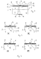
- Figures 1 - 3 are schematic cross-sectional views of electronic devices 1 having a semiconductor substrate 3.
- the semiconductor substrate 3 comprises a first zone 4, which is doped with n-type impurities, and a second zone 5, which is doped with p-type impurities. Only the first zone 4 of the substrate 3 is shown in figures 2 and 3 .
- the first and the second electrodes 8, 9 each comprise at least one epitaxial graphene monolayer 10.
- the at least one epitaxial graphene monolayer 10 of the first electrodes 8 is forming an ohmic contact with the substrate 3.
- a carbon buffer layer 12 is exhibited between the epitaxial graphene monolayer 10 of the first electrode 8 and the surface 7 of the substrate 3 .
- the at least one epitaxial graphene monolayer 10 of the second electrode 9 and the substrate 3 are forming a Schottky diode.
- a hydrogen layer 13 is shown between the epitaxial graphene monolayer 10 of the second electrode 9 and the surface 7 of the substrate 3 .
- the substrate 3 for example is a silicon carbide, in particular a mono crystal silicon carbide.
- the front surface 7 for example is a silicon terminated surface of the silicon carbide crystal, especially the (0001)-surface.
- the Invention however Is not limited to a silicon carbide as substrate 3 and also other surfaces can be used as front surfaces 7 of the substrate 3.
- the graphene layers 10 of the first electrodes 8 comprise so-called contact graphene layers.
- Contact graphene for example is prepared by thermal decomposition of a silicon terminated surface of silicon carbide.
- the graphene layer of the second electrode 9 comprises a so-called gate graphene layer.
- Gate graphene for example is prepared by hydrogen intercalation of contact graphene. Hydrogen saturates the dangling bonds of the surface 7 of the substrate 3.
- the carbon buffer layer 12 of a contact graphene Is converted to a quasi free-standing graphene monolayer. Therefore, the gate graphene of the second electrode 9 is shown with two graphene monolayers 10 in figures 1 to 3 .
- the shown devices 1 according to figures 1 to 3 are transistor elements T.
- the first electrodes 8 act as source electrode and as drain electrode.
- the second electrode 9 is acting as gate electrode of the transistor element T.
- a depletion layer or space charge region is formed within the substrate 3.
- the vertical width of the space charge region varies and the vertical depth of an n-type conductive layer 18 underneath the surface 7 of the substrate 3 increases or decreases with a decreasing or increasing space charge region of the n-p-junction.
- the electronic device 1 according to figure 2 is constructed as a "normally on"-device.
- the vertical depth of the n-type conductive layer 18 is large enough that the Schottky depletion layer 18 below the second gate graphene electrode 9 is not able to block the carrier transport within the conductive layer 18 between the first electrodes 8 ( figure 2a ).
- the Schottky depletion layer 19 expands spatially and is blocking the carrier transport within the conductive layer 18 between the first electrodes 8.
- the current path between the first electrodes 8 is completely narrowed down ( figure 2b ).
- the electronic device 1 according to figure 3 is constructed as a "normally off-device.
- the concentrations of the n-type and p-type impurities are chosen to get the space charge region at the n-p-junction within the substrate 3 broader towards the surface 7.
- the concentration of the n-type impurities is for example smaller than the concentration of the p-type impurities.
- the Schottky depletion layer 19 blocks the carrier transport within the thin conductive layer 18 between the first electrodes 8. Applying a slightly positive voltage to the second electrode 9, the Schottky depletion layer 19 becomes removed. Between the first electrodes 8 a current flows within the n-type conductive layer 18 of the substrate 3.
- an additional (back) electrode 16 is mounted in electrical contact with the second zone 5 of the substrate 3 one single electronic device 1 can be switched between a "normally on”-and a "normally-off”-device. Applying a voltage to the back electrode 16 will move the space charge region at the n-p-juncfion within the substrate 3 in/along a vertical direction.
- Figure 4 shows a top view of an exemplary embodiment of the electronic devices 1 as shown in figures 1 to 3 .
- the two first electrodes 8 are substantially sur rounded by strips of the second electrode 9.
- the second electrode 9 is a gate graphene electrode, these strips of the second electrode 9 block a carrier transport through the conductive layer within the substrate 3 away from the first electrodes 8.
- a locally decreased concentration of n-type Impurities below the strip of the second electrode 9 between the first electrodes 8 is preferred.
- the square formed contact pad of the second electrode 9 comprises a plurality of holes 20.
- the patterns of the electrodes 8, 9 including the holes are optimized to prepare all electrodes 8, 9 as contact graphene in a firstz step and to convert the second electrode 9 by hydrogen intercalation to gate graphene in a second step. Due to the diffusion controlled conversion of contact graphene into gate graphene by hydrogen intercalation the small strips of the second electrode 9 and also the contact pad of electrode 9 having holes are converted earller than the large areas of first electrodes 8. Stopping the hydrogen intercalation at this point of time, only the second electrode 9 and its corresponding strips are converted into gate graphene.
- FIG. 5 shows a top view of another exemplary embodiment of an electronic device 1 as shown in figures 1 to 3 .
- All electrodes 8, 9 have broad contact pads.
- the first electrode 8, acting as source electrode S, is completely surrounded by a ring shaped strip of the second electrode 9, which acts as a gate electrode G.
- the ring shaped strip of the second electrode 9 Is surrounded by another ring shaped strip of the other first electrode 8, which acts as drain electrode D.
- the current flow between the two first electrodes 8 is controlled by applying a voltage to the second gate electrode 9.
- the electrode pattern as shown in figure 5 is prepared by conversion of all electrodes 8. 9 from contact graphene to gate graphene (for example by hydrogen intercalation). Then, in a second step the first electrodes 8 are converted back into contact graphene by local laser heating.
- Figure 6 is a schematic cross-sectional view of an electronic device 1, acting as a single diode element DI.
- a first contact graphene electrode 8 is disposed adjoining a second gate graphene electrode 9. Both electrodes 8, 9 are separated from each other by a graphene free gap 15.
- the electronic device 1 as shown in figure 6 has the function of a unidirectional diode.
- the Schottky depletion layer 19 below the second electrode 9 allows current flow only in one direction.
- Figure 7 is a top view of an exemplary embodiment of a diode device 1 according to figure 6 .
- the first electrode 8 is surrounded by strips of the second electrode 9.
- the contact pad of the second electrode 9 comprises holes 20 to allow converting contact graphene into gate graphene by hydrogen intercalation. Additionally, the two adjoined electrodes 8, 9 form a capacitance. It is therefore possible to use to adjoined electrodes 8, 9 as a capacitor element C.
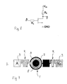
- Figure 8 is a circuit diagram of an electronic inverter. When a voltage V dd is applied to A. Y will be connected to ground. When applying ground to A, Y shows the voltage V dd .
- Figure 9 shows a top view of an exemplary embodiment for implementing the cir cuit as shown in figure 8 by using graphene electrodes on a semiconductor substrate.
- Two first electrodes 8 and a second electrode 9 in the middle are forming a transistor element T as shown in figure 5 .
- the ring shaped gate electrode 9 is connected to contact pad A via a resistor element R.
- the resistor element R is constructed by a strip having a meandering pattern.
- the ring shaped drain electrode 8 of the transistor element T is connected to a contact pad Y. This contact pad Y is connected to a second electrode pad V dd via a second resistor element R, also formed by a meandering pattern.
- the doping profile of the substrate is chosen such that the transistor element T is "normally off".
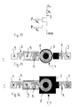
- Figure 10 shows a circuit diagram of a logical NAND-gate. Only in case of applying V dd to A and B, Y will be connected to ground.
- FIGs 11 to 14 show top views of exemplary embodiments for implementing the circuit as shown in figure 10 with graphene electrodes on the surface of a semiconductor substrate.
- the transistor elements T, T in the middle of all shown electrode patterns are drain-source-connected having two adjoined ring shaped second electrodes 9 between two first electrodes 8.
- the doping profile of the substrate is chosen such that the transistor element T, T is "normally off”.
- the electrode patterns according to figures 13 and 14 are space optimized.
- the electrode patterns of figures 12 and 14 are optimized to prepare the electrodes 8, 9 all as contact graphene electrodes in a first step and to convert the second electrodes 9 to gate graphene electrodes by hydrogen intercalation in a second step.
- the contact pad of the second electrodes 9, having a larger area than the strips, do comprise holes, which are not shown.
- the electrode patterns according to figures 11 and 13 are optimized to prepare the electrodes 8, 9 all as gate graphene electrodes, for example by hydrogen intercalation of contact graphene, and then to convert the first electrodes 8 by local heating back to contact graphene electrodes.
- Figure 15 shows a circuit diagram of a ring oscillator.
- a plurality of inverters such as shown in figures 8 and 9 is cascaded.
- the first inverter switches the second inverter.
- the last inverter in the chain switches back the first inverter. This results in an oscillation of the output Cl between V dd and ground with a specific measureable time constant.
- Figure 16 shows a top view of an exemplary embodiment of an implementation of the circuit according to figure 15 with a graphene electrode pattern on a semiconductor substrate.
- the broad contact pad for connecting ground to a first contact graphene electrode 8 and the broad contact pad for connecting V dd to a second gate graphene electrode 9 both are clearly shown.
- the square formed first electrodes 8 forming together with the ground electrode the source and drain electrodes of the cascaded transistors are clearly disclosed.
- the fingers 21 of the second electrodes 9 are forming the gate electrodes of the transistor elements T.
- the gate fingers 21 are disposed between two first contact graphene electrodes 8.
- the fingers 22 of the gate graphene electrodes 9 suppress unwanted cross-talk between the single transistor elements T.
- the source electrodes of the transistor elements T are connected with a small strip 23 adjoining the finger 22. Thereby, a defined resistance is created.
- the doping profile of the substrate is chosen such that the transistor elements T are "normally off”.
- Figure 17 displays a circuit diagram of a current regulation diode (CRD) or current limiting diode (CLD), which can be used as a constant current source for a load, which is connected between the anode connector A and the power supply V DD , while the cathode connector C is grounded.
- CCD current regulation diode
- CLD current limiting diode
- Figure 18 shows a top view of an exemplary embodiment of an implementation of the circuit according to figure 17 with a graphene electrode pattern on a semiconductor substrate.
- Two first electrodes 8 and a second electrode 9 In the middle are forming a transistor element T as shown in figure 5 .
- the ring shaped gate electrode is connected to contact pad C (cathode).
- the inner first electrode 8 (source electrode) is connected to contact pad C via a resistor element R.
- the resistor element R is constructed by a strip having a meandering pattern.
- the outer first electrode 8 (drain electrode) of the transistor element T Is connected to a contact pad A (anode).
- the doping profile of the substrate is chosen such that the transistor element T is "normally on”.
Landscapes
- Electrodes Of Semiconductors (AREA)
- Engineering & Computer Science (AREA)
- Power Engineering (AREA)
Abstract
Description
- The present invention relates to an electronic device having a first electrode and a second electrode disposed on the front surface of a semiconductor substrate, wherein the first electrode and the second electrode each comprises at least one epitaxial graphene monolayer. More specifically, the invention relates to an integrated circuit with silicon carbide (SiC) as semiconductor substrate and graphene layers on that substrate.
- Monolithic integrated circuits are electronic circults manufactured on one semiconductor substrate, comprising connected electronic devices like transistors, diodes, capacitors and resistors. Today, integrated circuits are mainly manufactured on the basis of Silicon (Si). However, other semiconductor materials may have advantages for specific application areas like high frequency or high power applications.
- Silicon carbide for example with a band gap of approximately 3eV has advantages for switching and controlling high power. Current technical applications of Silicon carbide are based on the principle of MOSFET's, JFET's or bipolar transistors. For such devices the silicon carbide substrate is doped with p-type and with n-type impurities.
- In the
WO 2005/001895 A2 an electronic device is disclosed, having a silicon carbide substrate and at least two graphene electrodes disposed on the surface of the substrate. In particular a transistor element is shown constructed by a graphene source electrode, a graphene drain electrode and a graphene gate electrode. These electrodes are disposed on the surface of the silicon carbide substrate. The drain electrode and the source electrode are bridged by a thin graphene strip. The gate electrode adjoins the thin graphene strip. Using the field effect the graphene In the thin strip is gated by applying a voltage to the graphene gate electrode. - In addition, the
WO 2009/158552 A2 discloses an electronic device constructed by graphene electrodes disposed on the surface of a silicon carbide substrate. The graphene of the electrodes is chemically modified. Graphene itself is gated as a thin strip also using the field effect. - Graphene as a single layer or monolayer of graphite shows an excellent carrier mobility as well as an excellent ampaclty. However, graphene exhibits no band gap; graphene is not a semiconductor. Graphene shows metallic conductivity. Due to the lack of a sufficiently large band gap, gating the graphene will therefore not result in an acceptable on/off-ratio of respective active devices. The on/off-ratio is Increased when using a thin graphene strip or by chemical modification of the graphene layers, where both methods result in disadvantages like the requirement of cryogenic operation temperatures or slow switching frequencies.
- Therefore, there is a need for an electronic device using graphene electrodes, which overcomes the mentioned disadvantages and is easy to fabricate.
- According to the invention the addressed problem is solved by an electronic device comprising a semiconductor substrate with a front surface, a first electrode and a second electrode both disposed on the front surface of the substrate. The first electrode and the second electrode each comprises at least one epitaxial graphene monolayer, wherein the at least one epitaxial graphene monolayer of the first electrode is forming an ohmic contact with the substrate and the at least one epitaxial graphene monolayer of the second electrode is forming a Schottky barrier with the substrate.
- The invention in a first step notices that based on the excellent electrical transport properties of graphene in active electronic devices graphene itself is used for the gated current path. Surprisingly, the invention is leaving this way and is using graphene electrodes for a current injection into the substrate. The current between the graphene electrodes is not flowing through graphene; the current between the graphene electrodes flows through the substrate.
- The new surprising concept or the invention allows using the excellent electrical properties of graphene without having the disadvantages of a low on/off-ratio due to the missing or small band gap of graphene. Instead the large band gap of the semiconducting substrate is employed. The current flow between two graphene electrodes is gated or controlled by changing the physical properties of the interface between the graphene and the substrate.
- For controlling the substrate current between graphene electrodes, the invention is using two types of graphene. The first type of graphene, the so-called "contact graphene", shows an ohmic contact with or into the substrate. The second type of graphene, the so-called "gate graphene", exhibits a Schottky barrier with or into the substrate. The first type of graphene allows a current flow between the graphene and the substrate as well as within the graphene Itself. The second type of graphene allows a current flow within the graphene but a current flow between the graphene and the substrate only is allowed in case of a respective voltage having applied to the graphene. The Schottky barrier between the second type of graphene and the substrate acts as a unidirectional diode. In addition, the Schottky barrier between the second type of graphene and the substrate according to the invention is used for controlling or gating the current path through the substrate. Depending on the applied voltage, the depletion layer of the Schottky diode underneath the second type of graphene is increased or decreased, thereby spatially varying the current path through a oonductive layer within the substrate.
- The first type of graphene or contact graphene is already known. This type of graphene for example is prepared by thermal decomposition of silicon carbide. However, also other preparation methods of contact graphene are conceivable. Heating a silicon carbide substrate to temperatures above the sublimation temperature of silicon (for example to 1700 °C In an Argon atmosphere) will result in the sublimation of silicon due to the lower vapor pressure of carbon as compared to silicon. After heating, the surface of the silicon carbide substrate exhibits one or few monolayers of epitaxial graphene. Preparation of contact graphene on the surface of silicon carbide for example is known from Nature Materials, Konstantin V. Emtsev, "Towards wafer-size Graphene Layers by Atmospheric Pressure Graphitization of Silicon carbide", Vol. 8, March 2009, p. 2003 to 2007. Epitaxial contact graphene preferably is prepared on the hexagonal (0001)-surface of the 6H-polytype of silicon carbide. However, other polytypes of silicon carbide and other surface orientations are also useable for the preparation of contact graphene layers. Also multi crystalline silicon carbide may be used. Since defects in the crystal would increase leakage currents, low grain sizes are not preferred.
- According to own investigations epitaxial contact graphene on silicon carbide shows a carrier mobility of 29.000 cm2/Vs and a carrier density of 1*1013 cm-2. Defects in the substrate will not considerably change these electrical properties. The ampacity of epitaxial graphene is around j = 4mA/µm. The conductivity of the graphene layer will increase when using more than one graphene layer stacked up to a graphitic layer. The injection barrier of contact graphene on silicon carbide is low.
- According to one embodiment of the invention the second type of epitaxial graphene or gate graphene is prepared from the first type of epitaxial graphene with atomic Intercalation. Allowing an appropriate atom or molecule to diffuse between the contact epitaxial graphene layer and the substrate might result in a graphene layer, which is quasi free standing on the surface of the substrate. The interface between the quasi free standing graphene layer and the semiconductor substrate exhibits a Schottky barrier according to a metal-semiconductor-junction,
- It is the main concept of the invention to have at least two electrodes on the surface of the substrate, wherein one of these electrodes comprises at least one epitaxial contact graphene monolayer, and the other electrode comprises at least one epitaxial gate graphene monolayer. The contact graphene layer shows an ohmic contact with the substrate. The gate graphene layer and the substrate are forming a Schottky diode. For preparation of the graphene layer showing an ohmic contact with the substrate and of a graphene layer forming a Schottky barrier with the substrate the use of other methods as currently known and described are possible; the invention is not limited to specific preparation methods. It is the ohmic contact and the Schottky barrier, which characterize the two types of graphene on the surface of the substrate.
- In case of preparing a contact graphene by thermal decomposition of silicon carbide, a structural analysis shows a carbon buffer layer between the first epitaxial graphene monolayer and the substrate. Part of the carbon atoms of the carbon buffer layer are chemically connected to silicon carbide by sp3 bonds, while the majority of carbon atoms of the carbon buffer layer are sp2 bonded within the layer, Within the epitaxial graphene monolayer the carbon atoms are arranged in a hexagonal pattern where each atom is chemically connected to its three neighbors by sp2 bonds. Crystalline graphite consists of stacked graphene layers. Some of the sp3 bonds of the surface of the substrate are so-called unsaturated dangling bonds. The electron in the valence shell is not shared with a carbon atom. Again it Is pointed out, that the buffer layer and the dangling bonds are features according to a preferred embodiment of the invention. Also other structural features of the interface between a graphene monolayer and a substrate may result in an ohmic contact between the graphene layer and the substrate.
- Preferably gate graphene is prepared by atomic intercalation of contact graphene. Useful atoms or molecules may saturate thereby the dangling bonds of the surface of the substrate. However, the carbon buffer layer changes by atomic Intercalation into a graphene monolayer, where the carbon atoms are connected with sp2 bonds with their three neighbors. This converted graphene monolayer is quasi free standing on the surface of the substrate. When preparing gate graphene by atomIc intercalation of contact graphene an intercalated atomic layer is disposed between the first epitaxial graphene monolayer and the surface of the substrate. At the interface between the gate graphene layer and the substrate a Schottky barrier will result.
- Own investigations show that diffusion controlled hydrogen intercalation of contact graphene by disposing the substrate for approximately 75 min in a hydrogen atmosphere at approximately 900 mbar at a temperature between 300°C and 600°C will result in a conversion of approximately 0.5 µm wide graphene strips to gate graphene. Larger areas of contact graphene will not be converted. Recently it has been investigated, that also atomic intercalation with Fluor and Gold will convert contact graphene Into gate graphene. And also appropriate other metals might be able to convert contact graphene.
- One possible preparation method of gate graphene is to convert contact graphene for example by hydrogen intercalation. However, it should be noted that it is also possible to convert gate graphene back into contact graphene. This is done for example by heating the quasi free-standing gate graphene and converting it back to a carbon buffer layer. If gate graphene has been prepared by hydrogen intercalation, the hydrogen will evaporate by local annealing above 900 °C. For the preparation of patterned contact graphene local laser heating of gate graphene is preferred.
- It is therefore possible to prepare patterned graphene layers on the semiconductor substrate by converting contact graphene to gate graphene or gate graphene to contact graphene locally. The manufacturing of these semiconductor devices is therefore simplified.
- The proposed semiconductor device is fully compatible with other semiconductor devices based on silicon carbide using the field effect for gating graphene and also with pure silicon carbide electronics and pure graphene electronics for high frequency applications. Integrated electronics based on a semiconductor device according to the invention have further several advantages over prior art, these include: Integrated electronic device structures can be prepared parallel on a single waver; preparation of Integrated electronic devices is possible using standard micro electronics lithography methods; preparation is possible with at least one single lithography step; graphene acts as a diffusion barrier blocking defects from the semiconductor substrate; high field strength's at edges are avoided due to the flat graphene layers; feature sizes as small as 1 µm scale are possible; there is no fundamental upper limitation of the feature size; operation under high temperature conditions and under harsh chemical and radiant environment is possible.
- Preferably the semiconductor substrate Is doped with impurities, wherein the impurity concentration within the semiconductor substrate varies in/along a vertical direction. In order to gate or to control the current flow through the substrate by applying a voltage to the second electrode, a current path near the surface of the substrate is preferred. A spatial expansion of the current path or a conductive layer Into the bulk is avoided by varying the concentration of the impurities in a/along vertical direction.
- According to one embodiment of the invention, the substrate is doped alternating with n-type and p-type impurities along the vertical direction. On each n-p-junction a depletion layer or space charge region is formed thereby limiting the horizontal depth of a conductive layer within the substrate. By applying a voltage to the second electrode the deletion layer will be changed allowing gating of the horizontal current flow through the substrate.
- According to another preferred embodiment of the invention along the vertical direction the semiconductor substrate comprises at least a first zone adjoining the front surface and a second zone at a distance from the front surface, wherein the substrate in the first zone and in the second zone is differently doped with impurities. Choosing the concentration of the impurities in the first zone different from the concentration of the impurities in the second zone moves the position of the depletion layer (along a vertical direction). If the concentration of the impurities in the first zone is lower as compared to the concentration of the impurities In the second zone, the depletion layer is moved towards the surface of the substrate. The n-type conductive layer in the first zone of the substrate is therefore narrowed in vertical direction.
- The invention allows constructing "normally on"-devices as well as "normally-off"-devices. If the conductive layer according to the depletion zone of a vertical n-p-junction is sufficiently narrowed in vertical direction, the Schottky barrier of a gate graphene layer on the surface may completely narrow down the current path and a "normally-off"-device results. Applying a slightly positive voltage on the gate graphene layer reduces the depth of the Schottky depletion layer and a horizontal current flow becomes allowed.
- Having a smaller depletion layer of the vertical n-p-junction within the substrate will result in a broader conductive layer underneath the surface of the substrate. The Schottky barrier of a gate graphene layer disposed on the surface is not able to stop a horizontal current flow through the conductive layer. However, if a negative voltage is applied to the gate graphene layer the depth of the Schottky depletion layer will increase and the current flow within the horizontal current path will be narrowed down. Having designed a smaller depletion layer will therefore result in a "normally-on"-devlce.
- According to a further embodiment of the invention the substrate In the first zone is doped with n-type impurities and is doped in the second zone with p-type impurities. This embodiment takes the advantage that a contact graphene layer shows the lowest injection barrier with regard to n-type silicon carbide. Alternatively, the substrate in the second zone is not doped with p-type impurities but is prepared to become semi-insulating. N-type doped silicon carbide (naturally due to the presence of N-atoms) for example is doped with vanadium, which traps electrons as major carriers in the n-type silicon carbide.
- Yet according to another embodiment of the invention the substrate comprises an additional electrode (for example a back electrode), which is connected to the second zone. Applying a voltage to the back electrode allows moving the depletion layer of the vertical n-p-junctton In the substrate vertically. With an additional (back) electrode it is therefore possible to switch one single device according to the invention between a "normally on" and a "normally off' state.
- It is not necessary to have an impurity concentration varying in the substrate in/along a horizontal direction. However, a horizontal variation of the impurity concentration allows a local variation of the depletion layer of an n-p-junction within the substrate. Thereby, the electrical transport properties of local positioned graphene elements could be changed and adapted. For example, depending on its lateral position, the same graphene structure is changed between a "normally on" and a "normally off" device by varying the impurity concentration in lateral direction. Also crossings of a graphene layer and a current path within the substrate are imaginable, increasing the impurity concentration in the substrate locally at the crossing point for example will decrease the gate effect of a crossing gate graphene thereby allowing a defined "cross-talk" between the graphene electrode and the current path below. According to a preferred embodiment of the invention the impurity concentration varies locally and laterally with the at least first and second electrodes.
- According to another preferred embodiment of the invention, the second electrode comprises a plurality of openings. When atomic, preferably hydrogen, intercalation is used for the preparation of gate graphene, these openings allow the atoms or hydrogen local penetration in addition to penetration at the edges of the graphene layer. Therefore, it is possible to convert large areas of contact graphene to gate graphene selectively. Large areas of contact graphene layers without holes/openings cannot be converted at same time, only small portions at the edges will be converted to gate graphene.
- According to another embodiment of the invention, a third electrode is disposed on the front surface of the substrate, the third electrode also being comprised of at least one epitaxial graphene monolayer. This allows the construction of active devices where for example one of these three electrodes is used for gating or controlling a current between the other two electrodes.
- The invention allows integrated construction of active and passive electronic devices. According to one embodiment of the invention a transistor element is comprised, the transistor element having at least the first electrode, the second electrode and the third electrode, wherein the second electrode is disposed between the first and the third electrode on the front surface of the substrate. Preferably, the at least one epitaxial graphene monolayer of the second electrode is a gate graphene forming a Schottky barrier with the substrate. The first and the third electrode act as source and drain electrode. The current flow between the first and the third electrode through the substrate is controlled by the second (gate) electrode. Applying a voltage to the gate electrode changes the Schottky depletion layer in the substrate and therefore changes the current flow.
- According to another preferred embodiment of the invention, a capacitor element is comprised. The capacitor element is constructed by at least one single second electrode and the substrate, having the capacitance of the Schottky depletion layer between the at least one epitaxial graphene layer of the second electrode and the substrate, or is constructed by at least two separated second electrodes, the two second electrodes adjoining each other, or is constructed by at least one single second electrode, a dielectric medium and a metal electrode, the dielectric medium being sandwiched between the second electrode and the metal electrode,
- Preferably the electronic device comprises a resistor element, which is constructed by at least one strip of the at least one first or second electrode. The resistance of such a graphene strip is calculated from the known resistance of the graphene layer and the given length or geometry of the strip. One additional advantage of the invention in that context is that there is no contact resistance at a contact-gate-graphene junction. Therefore, gate graphene and contact graphene therefore may be connected to each other without considering electric transport properties of a junction of both graphene types. Alternatively or additionally the resistance of the conductive layer within the substrate is used. To yield a defined resistance of the conductive layer the current path for example is spatially narrowed by a second electrode having a gate graphene layer or by a appropriate lateral doping profile.
- In a preferred embodiment of the invention, the resistor strip has a meandering pattern. This allows a packed construction of the resistor element.
- According to another embodiment of the invention the first electrode is substantially surrounded by the second electrode. The surrounding second electrode confines the current paths to and from the first electrode through the conductive layer of the substrate. A ring shaped second electrode for example is preferred when all possible current paths to and from the first electrode should be narrowed down in an off state of the device. The surrounding second electrode is also used to align the current flow within the conductive layer of the substrate.
- Advantageously the electronic device comprises at least one conductor strip, which is formed by a second electrode strip or by a first electrode strip which is surrounded by a second electrode strip. Both embodiments avoid leakage currents through the substrate when connecting the graphene electrodes to said conductor strips electrically. Alternatively other metal strips may be used for the electrical connection of the graphene layers.
- According to another preferred embodiment of the invention, the electronic device is an integrated circuit, wherein a plurality of first and second electrodes is comprised, at least two of these electrodes being electrically connected by a current path through the substrate.
- These and various other features of the present invention will become better understood upon reading of the following description of preferred embodiments in conjunction with the accompanying drawings.
- Fig. 1-3
- are schematic cross-sectional views of electronic devices with a gate graphene electrode disposed between two contact graphene electrodes on the front surface of a semiconductor substrate,
- Fig. 4-5
- are schematic top views of electronic devices according to
Fig. 1-3 , - Fig. 6
- Is a schematic cross-sectional view of an electronic device with a gate graphene electrode and a contact graphene electrode disposed on the front surface of a semiconductor substrate.
- Fig. 7
- Is a schematic top view of an electronic device according to
Fig. 6 , - Fig. 8
- is a circuit diagram of an Inverter,
- Fig. 9
- is a schematic top view of an electronic device with a plurality of gate and contact graphene electrodes on the front surface of a substrate implementing the circuit diagram of
Fig. 8 , - Fig. 10
- is a circuit diagram of an electronic NAND-gate,
- Fig. 11-14
- are schematic top views of electronic devices with a plurality of gate and contact graphene electrodes on the front surface of a substrate implementing the circuit diagram of
Fig. 10 , - Fig. 15
- is a circuit diagram of an electronic ring oscillator,
- Fig. 16
- is a schematic top view of an electronic device with a plurality of gate and contact graphene electrodes on the front surface of a substrate implementing the circuit diagram of
Fig. 15 . - Fig. 17
- is a circuit diagram of a current regulation diode (CRD) or current limiting diode (CLD), and
- Fig. 18
- is a schematic top view of an electronic device with a plurality of gate and contact graphene electrodes on the front surface of a substrate implementing the circuit diagram of
Fig. 17 . -
Figures 1 - 3 are schematic cross-sectional views ofelectronic devices 1 having asemiconductor substrate 3. Thesemiconductor substrate 3 comprises afirst zone 4, which is doped with n-type impurities, and asecond zone 5, which is doped with p-type impurities. Only thefirst zone 4 of thesubstrate 3 is shown infigures 2 and 3 . - On the
front surface 7 of thesubstrate 3 twofirst electrodes 8 and asecond electrode 9 are disposed. Thesecond electrode 9 Is disposed between the twofirst electrodes 8. The first and thesecond electrodes epitaxial graphene monolayer 10. The at least oneepitaxial graphene monolayer 10 of thefirst electrodes 8 is forming an ohmic contact with thesubstrate 3. Between theepitaxial graphene monolayer 10 of thefirst electrode 8 and thesurface 7 of the substrate 3 acarbon buffer layer 12 is exhibited. The at least oneepitaxial graphene monolayer 10 of thesecond electrode 9 and thesubstrate 3 are forming a Schottky diode. Between theepitaxial graphene monolayer 10 of thesecond electrode 9 and thesurface 7 of the substrate 3 ahydrogen layer 13 is shown. - The
substrate 3 for example is a silicon carbide, in particular a mono crystal silicon carbide. Thefront surface 7 for example is a silicon terminated surface of the silicon carbide crystal, especially the (0001)-surface. The Invention however Is not limited to a silicon carbide assubstrate 3 and also other surfaces can be used asfront surfaces 7 of thesubstrate 3. - The graphene layers 10 of the
first electrodes 8 comprise so-called contact graphene layers. Contact graphene for example is prepared by thermal decomposition of a silicon terminated surface of silicon carbide. The graphene layer of thesecond electrode 9 comprises a so-called gate graphene layer. Gate graphene for example is prepared by hydrogen intercalation of contact graphene. Hydrogen saturates the dangling bonds of thesurface 7 of thesubstrate 3. Thecarbon buffer layer 12 of a contact graphene Is converted to a quasi free-standing graphene monolayer. Therefore, the gate graphene of thesecond electrode 9 is shown with twographene monolayers 10 infigures 1 to 3 . - The shown
devices 1 according tofigures 1 to 3 are transistor elements T. Thefirst electrodes 8 act as source electrode and as drain electrode. Thesecond electrode 9 is acting as gate electrode of the transistor element T. - At the boundary between the first n-
type zone 4 and the second p-type zone 5 a depletion layer or space charge region is formed within thesubstrate 3. Depending on the concentration of the n-type and p-type impurities the vertical width of the space charge region varies and the vertical depth of an n-type conductive layer 18 underneath thesurface 7 of thesubstrate 3 increases or decreases with a decreasing or increasing space charge region of the n-p-junction. - The
electronic device 1 according tofigure 2 is constructed as a "normally on"-device. The vertical depth of the n-type conductive layer 18 is large enough that theSchottky depletion layer 18 below the secondgate graphene electrode 9 is not able to block the carrier transport within theconductive layer 18 between the first electrodes 8 (figure 2a ). - If a negative voltage is applied to the
second electrode 9, theSchottky depletion layer 19 expands spatially and is blocking the carrier transport within theconductive layer 18 between thefirst electrodes 8. The current path between thefirst electrodes 8 is completely narrowed down (figure 2b ). - The
electronic device 1 according tofigure 3 is constructed as a "normally off-device. The concentrations of the n-type and p-type impurities are chosen to get the space charge region at the n-p-junction within thesubstrate 3 broader towards thesurface 7. The concentration of the n-type impurities is for example smaller than the concentration of the p-type impurities. - Having no voltage applied to the second electrode 9 (
figure 3b ), theSchottky depletion layer 19 blocks the carrier transport within the thinconductive layer 18 between thefirst electrodes 8. Applying a slightly positive voltage to thesecond electrode 9, theSchottky depletion layer 19 becomes removed. Between the first electrodes 8 a current flows within the n-type conductive layer 18 of thesubstrate 3. - If an additional (back)
electrode 16 is mounted in electrical contact with thesecond zone 5 of thesubstrate 3 one singleelectronic device 1 can be switched between a "normally on"-and a "normally-off"-device. Applying a voltage to theback electrode 16 will move the space charge region at the n-p-juncfion within thesubstrate 3 in/along a vertical direction. -
Figure 4 shows a top view of an exemplary embodiment of theelectronic devices 1 as shown infigures 1 to 3 . The twofirst electrodes 8 are substantially sur rounded by strips of thesecond electrode 9. As thesecond electrode 9 is a gate graphene electrode, these strips of thesecond electrode 9 block a carrier transport through the conductive layer within thesubstrate 3 away from thefirst electrodes 8. In case of a "normally off'-device a locally decreased concentration of n-type Impurities below the strip of thesecond electrode 9 between thefirst electrodes 8 is preferred. The square formed contact pad of thesecond electrode 9 comprises a plurality ofholes 20. The patterns of theelectrodes electrodes second electrode 9 by hydrogen intercalation to gate graphene in a second step. Due to the diffusion controlled conversion of contact graphene into gate graphene by hydrogen intercalation the small strips of thesecond electrode 9 and also the contact pad ofelectrode 9 having holes are converted earller than the large areas offirst electrodes 8. Stopping the hydrogen intercalation at this point of time, only thesecond electrode 9 and its corresponding strips are converted into gate graphene. -
Figure 5 shows a top view of another exemplary embodiment of anelectronic device 1 as shown infigures 1 to 3 . Allelectrodes first electrode 8, acting as source electrode S, is completely surrounded by a ring shaped strip of thesecond electrode 9, which acts as a gate electrode G. The ring shaped strip of thesecond electrode 9 Is surrounded by another ring shaped strip of the otherfirst electrode 8, which acts as drain electrode D. As explained with regard tofigures 1 - 4 the current flow between the twofirst electrodes 8 is controlled by applying a voltage to thesecond gate electrode 9. - The electrode pattern as shown in
figure 5 is prepared by conversion of allelectrodes 8. 9 from contact graphene to gate graphene (for example by hydrogen intercalation). Then, in a second step thefirst electrodes 8 are converted back into contact graphene by local laser heating. -
Figure 6 is a schematic cross-sectional view of anelectronic device 1, acting as a single diode element DI. On thefront surface 7 of the substrate 3 a firstcontact graphene electrode 8 is disposed adjoining a secondgate graphene electrode 9. Bothelectrodes free gap 15. - The
electronic device 1 as shown infigure 6 has the function of a unidirectional diode. TheSchottky depletion layer 19 below thesecond electrode 9 allows current flow only in one direction. -
Figure 7 is a top view of an exemplary embodiment of adiode device 1 according tofigure 6 . Thefirst electrode 8 is surrounded by strips of thesecond electrode 9. The contact pad of thesecond electrode 9 comprisesholes 20 to allow converting contact graphene into gate graphene by hydrogen intercalation. Additionally, the two adjoinedelectrodes electrodes -
Figure 8 is a circuit diagram of an electronic inverter. When a voltage Vdd is applied to A. Y will be connected to ground. When applying ground to A, Y shows the voltage Vdd. -
Figure 9 shows a top view of an exemplary embodiment for implementing the cir cuit as shown infigure 8 by using graphene electrodes on a semiconductor substrate. Twofirst electrodes 8 and asecond electrode 9 in the middle are forming a transistor element T as shown infigure 5 . The ring shapedgate electrode 9 is connected to contact pad A via a resistor element R. The resistor element R is constructed by a strip having a meandering pattern. The ring shapeddrain electrode 8 of the transistor element T is connected to a contact pad Y. This contact pad Y is connected to a second electrode pad Vdd via a second resistor element R, also formed by a meandering pattern. The doping profile of the substrate is chosen such that the transistor element T is "normally off". -
Figure 10 shows a circuit diagram of a logical NAND-gate. Only in case of applying Vdd to A and B, Y will be connected to ground. -
Figures 11 to 14 show top views of exemplary embodiments for implementing the circuit as shown infigure 10 with graphene electrodes on the surface of a semiconductor substrate. The transistor elements T, T in the middle of all shown electrode patterns are drain-source-connected having two adjoined ring shapedsecond electrodes 9 between twofirst electrodes 8. The doping profile of the substrate is chosen such that the transistor element T, T is "normally off". - The electrode patterns according to
figures 13 and14 are space optimized. The electrode patterns offigures 12 and14 are optimized to prepare theelectrodes second electrodes 9 to gate graphene electrodes by hydrogen intercalation in a second step. For this purpose the contact pad of thesecond electrodes 9, having a larger area than the strips, do comprise holes, which are not shown. - The electrode patterns according to
figures 11 and13 are optimized to prepare theelectrodes first electrodes 8 by local heating back to contact graphene electrodes. -
Figure 15 shows a circuit diagram of a ring oscillator. A plurality of inverters such as shown infigures 8 and 9 is cascaded. The first inverter switches the second inverter. The last inverter in the chain switches back the first inverter. This results in an oscillation of the output Cl between Vdd and ground with a specific measureable time constant. -
Figure 16 shows a top view of an exemplary embodiment of an implementation of the circuit according tofigure 15 with a graphene electrode pattern on a semiconductor substrate. The broad contact pad for connecting ground to a firstcontact graphene electrode 8 and the broad contact pad for connecting Vdd to a secondgate graphene electrode 9 both are clearly shown. Also the square formedfirst electrodes 8 forming together with the ground electrode the source and drain electrodes of the cascaded transistors are clearly disclosed. Thefingers 21 of thesecond electrodes 9 are forming the gate electrodes of the transistor elements T. Thegate fingers 21 are disposed between two firstcontact graphene electrodes 8. Thefingers 22 of thegate graphene electrodes 9 suppress unwanted cross-talk between the single transistor elements T. The source electrodes of the transistor elements T are connected with asmall strip 23 adjoining thefinger 22. Thereby, a defined resistance is created. The doping profile of the substrate is chosen such that the transistor elements T are "normally off". -
Figure 17 displays a circuit diagram of a current regulation diode (CRD) or current limiting diode (CLD), which can be used as a constant current source for a load, which is connected between the anode connector A and the power supply VDD, while the cathode connector C is grounded. -
Figure 18 shows a top view of an exemplary embodiment of an implementation of the circuit according tofigure 17 with a graphene electrode pattern on a semiconductor substrate. Twofirst electrodes 8 and asecond electrode 9 In the middle are forming a transistor element T as shown infigure 5 . The ring shaped gate electrode is connected to contact pad C (cathode). The inner first electrode 8 (source electrode) is connected to contact pad C via a resistor element R. The resistor element R is constructed by a strip having a meandering pattern. The outer first electrode 8 (drain electrode) of the transistor element T Is connected to a contact pad A (anode). The doping profile of the substrate is chosen such that the transistor element T is "normally on".
Claims (21)
- An electronic device (1) comprising:- a semiconductor substrate (3) having a front surface (7).- a first electrode (8) and a second electrode (9) disposed on the front surface (7) of the substrate (3), wherein the first electrode (8) and the second electrode (9) each comprises at least one epitaxial graphene monolayer (10),characterized In that- the at least one epitaxial graphene monolayer (10) of the first electrode (8) is forming an ohmic contact with the substrate (3) and- the at least one epitaxial graphene monolayer (10) of the second electrode (9) Is forming a Schottky barrier with the substrate (3).
- The electronic device (1) according to claim 1, wherein a carbon buffer layer (12) is disposed between the at least one epitaxial graphene monolayer (10) of the first electrode (8) and the substrate (3), and wherein the surface (7) of the substrate (3) comprises a plurality of dangling bonds.
- The electronic device (1) according to claim 1 or 2, wherein an intercalated atomic layer (13) is disposed between the at least one epitaxial graphene monolayer (10) of the second electrode (9) and the substrate (3).
- The electronic device (1) according to claim 3, wherein the intercalated atomic layer(13) is a Hydrogen layer, a Fluor layer and/or a Gold layer,
- The electronic device (1) according to any of the preceding claims, wherein the semiconductor substrate (3) is doped with impurities, and wherein the impurity concentration within the semiconductor substrate (3) varies in/along a vertical direction.
- The electronic device (1) according to claim 5, wherein along the vertical direction the semiconductor substrate (3) comprises at least a first zone (4) adjoining the front surface and a second zone (5) at a distance from the front surface (7), and wherein the substrate (3) in the first zone (4) and in the second zone (5) is differently doped with impurities.
- The electronic device (1) according to claim 6, wherein the substrate (3) is doped in the first zone (4) with n-type impurities, and wherein the substrate (3) is doped with p-type impurities or is semi-insulating In the second zone (5).
- The electronic device (1) according to claim 6 or 7, wherein the substrate (3) comprises an additional electrode (16), which is electrically connected with the second zone (5).
- The electronic device (1) according to any of the preceding claims, wherein the semiconductor substrate (3) is doped with impurities, and wherein the impurity concentration within the semiconductor substrate (3) varies in/along a horizontal direction.
- The electronic device (1) according to claim 9, wherein the impurity concentration varies in/along at least one horizontal direction with the at least first and second electrode (8, 9).
- The electronic device (1) according to any of the preceding claims, wherein the semiconductor substrate (3) is a silicon carbide (SIC).
- The electronic device (1) according to claim 11, wherein the silicon carbide is a single crystal silicon carbide, and wherein the surface region is on the Si terminated (0001) surface of the single crystal silicon carbide.
- The electronic device (1) according to any of the preceding claims, wherein the second electrode (9) comprises a plurality of openings (20).
- The electronic device (1) according to any of the preceding claims, wherein the first electrode (8) is substantially surrounded by the second electrode (9).
- The electronic device (1) according to any of the preceding claims, wherein a third electrode is disposed on the front surface (7) of the substrate (3), the third electrode also being comprised of at least one epitaxial graphene monolayer (10).
- The electronic device (1) according to claim 15, wherein a transistor element (T) is comprised, the transistor element (T) having at least the first electrode (8), the third electrode and the second electrode (9), wherein the second electrode (9) is disposed between the first (8) and the third electrode on the front surface (7) of the surface (3).
- The electronic device (1) according to any of the preceding claims, wherein a capacitor element (C) is comprised, the capacitor element (C) being constructed by:- at least one single second electrode (9) and the substrate (3), having the capacitance of the Schottky barrier between the at least one epitaxial graphene layer of the second electrode (9) and the substrate (3),- at least two separated second electrodes (9), the two second electrodes (9) adjoining each other, and/or- at least one single second electrode (9), a dielectric medium and a metal electrode, the dielectric medium being sandwiched between the second electrode (9) and the metal electrode,
- The electronic device (1) according to any of the preceding claims, wherein a resistor element (R) is comprised, the resistor element (R) being formed by at least one strip of the at least one first electrode (8) or second electrode (9).
- The electronic device (1) according to claim 18, wherein the strip has a meandering pattern.
- The electronic device (1) according to any of the preceding claims, wherein at least one conductor strip is comprised, the conductor strip being formed by a second electrode strip (9) or by a first electrode strip (8) which Is surrounded by a second electrode strip (9).
- The electronic device (1) according to any of the preceding claims, wherein a plurality of first and second electrodes (8, 9) is comprised, at least two of these electrodes (8, 9) being electrically connected by a current path through the substrate (3).
Priority Applications (4)
| Application Number | Priority Date | Filing Date | Title |
|---|---|---|---|
| EP11004981.4A EP2535937B1 (en) | 2011-06-17 | 2011-06-17 | Electronic device |
| US14/124,274 US9269774B2 (en) | 2011-06-17 | 2012-06-18 | Electronic device |
| PCT/EP2012/002572 WO2012171665A1 (en) | 2011-06-17 | 2012-06-18 | Electronic device |
| EP12733591.7A EP2721639A1 (en) | 2011-06-17 | 2012-06-18 | Electronic device |
Applications Claiming Priority (1)
| Application Number | Priority Date | Filing Date | Title |
|---|---|---|---|
| EP11004981.4A EP2535937B1 (en) | 2011-06-17 | 2011-06-17 | Electronic device |
Publications (2)
| Publication Number | Publication Date |
|---|---|
| EP2535937A1 true EP2535937A1 (en) | 2012-12-19 |
| EP2535937B1 EP2535937B1 (en) | 2015-03-11 |
Family
ID=45350567
Family Applications (2)
| Application Number | Title | Priority Date | Filing Date |
|---|---|---|---|
| EP11004981.4A Not-in-force EP2535937B1 (en) | 2011-06-17 | 2011-06-17 | Electronic device |
| EP12733591.7A Withdrawn EP2721639A1 (en) | 2011-06-17 | 2012-06-18 | Electronic device |
Family Applications After (1)
| Application Number | Title | Priority Date | Filing Date |
|---|---|---|---|
| EP12733591.7A Withdrawn EP2721639A1 (en) | 2011-06-17 | 2012-06-18 | Electronic device |
Country Status (3)
| Country | Link |
|---|---|
| US (1) | US9269774B2 (en) |
| EP (2) | EP2535937B1 (en) |
| WO (1) | WO2012171665A1 (en) |
Families Citing this family (9)
| Publication number | Priority date | Publication date | Assignee | Title |
|---|---|---|---|---|
| DE102011016900A1 (en) * | 2011-04-13 | 2012-10-18 | Friedrich-Alexander-Universität Erlangen-Nürnberg | Semiconductor device |
| US8969154B2 (en) * | 2011-08-23 | 2015-03-03 | Micron Technology, Inc. | Methods for fabricating semiconductor device structures and arrays of vertical transistor devices |
| US10217819B2 (en) * | 2015-05-20 | 2019-02-26 | Samsung Electronics Co., Ltd. | Semiconductor device including metal-2 dimensional material-semiconductor contact |
| US10586864B2 (en) | 2018-08-05 | 2020-03-10 | International Business Machines Corporation | Vertical transistor with one-dimensional edge contacts |
| US10593798B2 (en) * | 2018-08-05 | 2020-03-17 | International Business Machines Corporation | Vertical transistor with one atomic layer gate length |
| US12247923B2 (en) * | 2019-04-25 | 2025-03-11 | The Penn State Research Foundation | Graphene hybrids for biological and chemical sensing |
| DE102019123248B4 (en) | 2019-08-29 | 2025-04-24 | Friedrich-Alexander-Universität Erlangen-Nürnberg | Electron source for generating an electron beam |
| US20240234588A1 (en) * | 2023-01-11 | 2024-07-11 | University Of South Carolina | Self-biased mo/n-4h-sic schottky barriers as high-performance ultraviolet photodetectors |
| CN118198064B (en) * | 2024-05-20 | 2024-09-17 | 天津大学 | Graphene-based all-carbon logic circuit and preparation method thereof |
Family Cites Families (8)
| Publication number | Priority date | Publication date | Assignee | Title |
|---|---|---|---|---|
| US3780320A (en) * | 1971-12-20 | 1973-12-18 | Ibm | Schottky barrier diode read-only memory |
| US3849789A (en) * | 1972-11-01 | 1974-11-19 | Gen Electric | Schottky barrier diodes |
| DE2755433C2 (en) * | 1977-12-13 | 1986-09-25 | Telefunken electronic GmbH, 7100 Heilbronn | Radiation-emitting semiconductor diode |
| JPS57166068A (en) * | 1981-04-07 | 1982-10-13 | Toshiba Corp | Semiconductor device |
| US5047826A (en) * | 1989-06-30 | 1991-09-10 | Texas Instruments Incorporated | Gigaohm load resistor for BICMOS process |
| JPH09205198A (en) * | 1996-01-24 | 1997-08-05 | Toyota Motor Corp | Field effect semiconductor device and method of manufacturing semiconductor device |
| US7015142B2 (en) | 2003-06-12 | 2006-03-21 | Georgia Tech Research Corporation | Patterned thin film graphite devices and method for making same |
| EP2311078A4 (en) | 2008-06-26 | 2012-11-21 | Carben Semicon Ltd | INTEGRATED PATTERNED CIRCUIT AND METHOD FOR PRODUCING THE SAME |
-
2011
- 2011-06-17 EP EP11004981.4A patent/EP2535937B1/en not_active Not-in-force
-
2012
- 2012-06-18 EP EP12733591.7A patent/EP2721639A1/en not_active Withdrawn
- 2012-06-18 WO PCT/EP2012/002572 patent/WO2012171665A1/en not_active Ceased
- 2012-06-18 US US14/124,274 patent/US9269774B2/en not_active Expired - Fee Related
Non-Patent Citations (3)
| Title |
|---|
| GIANNAZZO F ET AL: "Lateral uniformity of the transport properties of graphene/4H-SiC (0001) interface by nanoscale current measurements", MATERIALS RESEARCH SOCIETY SYMPOSIUM PROCEEDINGS - LARGE-AREA ELECTRONICS FROM CARBON NANOTUBES, GRAPHENE, AND RELATED NONCARBON NANOSTRUCTURES 2010 MATERIALS RESEARCH SOCIETY USA, vol. 1205, 30 November 2009 (2009-11-30), pages 20 - 25, XP002667517 * |
| TONGAY S ET AL: "Tuning Schottky diodes at the many-layer-graphene/semiconductor interface by doping", CARBON ELSEVIER SCIENCE LTD. UK, vol. 49, no. 6, May 2011 (2011-05-01), pages 2033 - 2038, XP002667516, ISSN: 0008-6223 * |
| XIAOSONG WU ET AL: "Epitaxial-graphene/graphene-oxide junction: an essential step towards epitaxial graphene electronics", PHYSICAL REVIEW LETTERS, AMERICAN PHYSICAL SOCIETY, NEW YORK, US, vol. 101, no. 2, 11 July 2008 (2008-07-11), pages 26801/1 - 4, XP009138386, ISSN: 0031-9007, [retrieved on 20080707], DOI: 10.1103/PHYSREVLETT.101.026801 * |
Also Published As
| Publication number | Publication date |
|---|---|
| EP2721639A1 (en) | 2014-04-23 |
| US20140225066A1 (en) | 2014-08-14 |
| WO2012171665A1 (en) | 2012-12-20 |
| EP2535937B1 (en) | 2015-03-11 |
| US9269774B2 (en) | 2016-02-23 |
Similar Documents
| Publication | Publication Date | Title |
|---|---|---|
| EP2535937B1 (en) | Electronic device | |
| Hertel et al. | Tailoring the graphene/silicon carbide interface for monolithic wafer-scale electronics | |
| Oh et al. | Electrical characteristics of vertical Ni/β-Ga2O3 Schottky barrier diodes at high temperatures | |
| US6524900B2 (en) | Method concerning a junction barrier Schottky diode, such a diode and use thereof | |
| Umezawa et al. | High temperature application of diamond power device | |
| JP6855700B2 (en) | Semiconductor devices and their manufacturing methods | |
| KR102216543B1 (en) | Graphene-Metal bonding structure and method of manufacturing the same, and semiconductor device having graphene-Metal bonding structure | |
| CN102738227B (en) | Sic semiconductor power device | |
| TW201117379A (en) | Semiconductor devices including electrodes with integrated resistances and related methods | |
| JP2002203967A (en) | Semiconductor element | |
| JP2015115373A (en) | Semiconductor apparatus, and manufacturing method of semiconductor apparatus | |
| CN104979395A (en) | Semiconductor structure | |
| US9722029B2 (en) | Semiconductor device and method of manufacturing semiconductor device | |
| CN108899369B (en) | Graphene channel silicon carbide power semiconductor transistor | |
| WO2017183375A1 (en) | Semiconductor device | |
| JP2022003711A (en) | Semiconductor device | |
| JP2019029501A (en) | Semiconductor device and manufacturing method of semiconductor device | |
| WO2014002597A1 (en) | Silicon carbide semiconductor device | |
| US20230079069A1 (en) | Electronic device | |
| US9263526B2 (en) | Semiconductor component | |
| JP7411465B2 (en) | semiconductor equipment | |
| JP4045893B2 (en) | Vertical junction field effect transistor | |
| CN106158943A (en) | N ditch carborundum SITH and manufacture method thereof | |
| Zhang et al. | VdW Heterostructure Electronics | |
| CN108565294A (en) | A kind of silicon carbide diode and preparation method thereof of epitaxial layer varying doping concentration |
Legal Events
| Date | Code | Title | Description |
|---|---|---|---|
| PUAI | Public reference made under article 153(3) epc to a published international application that has entered the european phase |
Free format text: ORIGINAL CODE: 0009012 |
|
| 17P | Request for examination filed |
Effective date: 20120313 |
|
| AK | Designated contracting states |
Kind code of ref document: A1 Designated state(s): AL AT BE BG CH CY CZ DE DK EE ES FI FR GB GR HR HU IE IS IT LI LT LU LV MC MK MT NL NO PL PT RO RS SE SI SK SM TR |
|
| AX | Request for extension of the european patent |
Extension state: BA ME |
|
| RIN1 | Information on inventor provided before grant (corrected) |
Inventor name: WALDMANN, DANIEL Inventor name: KRIEGER, MICHAEL Inventor name: JOBST, JOHANNES Inventor name: KRACH, FLORIAN Inventor name: HERTEL, STEFAN Inventor name: WEBER, HEIKO B. |
|
| RIC1 | Information provided on ipc code assigned before grant |
Ipc: H01L 29/47 20060101AFI20140815BHEP Ipc: H01L 21/329 20060101ALI20140815BHEP Ipc: H01L 21/338 20060101ALI20140815BHEP Ipc: H01L 29/872 20060101ALI20140815BHEP Ipc: H01L 27/12 20060101ALI20140815BHEP Ipc: H01L 21/84 20060101ALI20140815BHEP Ipc: H01L 27/105 20060101ALI20140815BHEP Ipc: H01L 29/423 20060101ALI20140815BHEP Ipc: H01L 29/417 20060101ALI20140815BHEP Ipc: H01L 21/02 20060101ALI20140815BHEP Ipc: H01L 27/06 20060101ALI20140815BHEP Ipc: H01L 29/16 20060101ALN20140815BHEP Ipc: H01L 29/812 20060101ALI20140815BHEP Ipc: H01L 29/45 20060101ALI20140815BHEP Ipc: H01L 21/82 20060101ALI20140815BHEP |
|
| RIC1 | Information provided on ipc code assigned before grant |
Ipc: H01L 29/16 20060101ALN20140826BHEP Ipc: H01L 29/872 20060101ALI20140826BHEP Ipc: H01L 29/812 20060101ALI20140826BHEP Ipc: H01L 29/47 20060101AFI20140826BHEP Ipc: H01L 27/12 20060101ALI20140826BHEP Ipc: H01L 21/338 20060101ALI20140826BHEP Ipc: H01L 29/417 20060101ALI20140826BHEP Ipc: H01L 29/423 20060101ALI20140826BHEP Ipc: H01L 21/82 20060101ALI20140826BHEP Ipc: H01L 29/45 20060101ALI20140826BHEP Ipc: H01L 27/06 20060101ALI20140826BHEP Ipc: H01L 27/105 20060101ALI20140826BHEP Ipc: H01L 21/329 20060101ALI20140826BHEP Ipc: H01L 21/84 20060101ALI20140826BHEP Ipc: H01L 21/02 20060101ALI20140826BHEP |
|
| GRAP | Despatch of communication of intention to grant a patent |
Free format text: ORIGINAL CODE: EPIDOSNIGR1 |
|
| INTG | Intention to grant announced |
Effective date: 20141006 |
|
| GRAS | Grant fee paid |
Free format text: ORIGINAL CODE: EPIDOSNIGR3 |
|
| GRAA | (expected) grant |
Free format text: ORIGINAL CODE: 0009210 |
|
| AK | Designated contracting states |
Kind code of ref document: B1 Designated state(s): AL AT BE BG CH CY CZ DE DK EE ES FI FR GB GR HR HU IE IS IT LI LT LU LV MC MK MT NL NO PL PT RO RS SE SI SK SM TR |
|
| REG | Reference to a national code |
Ref country code: GB Ref legal event code: FG4D |
|
| REG | Reference to a national code |
Ref country code: CH Ref legal event code: EP |
|
| REG | Reference to a national code |
Ref country code: IE Ref legal event code: FG4D |
|
| REG | Reference to a national code |
Ref country code: AT Ref legal event code: REF Ref document number: 715734 Country of ref document: AT Kind code of ref document: T Effective date: 20150415 |
|
| REG | Reference to a national code |
Ref country code: DE Ref legal event code: R096 Ref document number: 602011014518 Country of ref document: DE Effective date: 20150423 |
|
| REG | Reference to a national code |
Ref country code: NL Ref legal event code: VDEP Effective date: 20150311 |
|
| REG | Reference to a national code |
Ref country code: NL Ref legal event code: VDEP Effective date: 20150311 |
|
| PG25 | Lapsed in a contracting state [announced via postgrant information from national office to epo] |
Ref country code: HR Free format text: LAPSE BECAUSE OF FAILURE TO SUBMIT A TRANSLATION OF THE DESCRIPTION OR TO PAY THE FEE WITHIN THE PRESCRIBED TIME-LIMIT Effective date: 20150311 Ref country code: FI Free format text: LAPSE BECAUSE OF FAILURE TO SUBMIT A TRANSLATION OF THE DESCRIPTION OR TO PAY THE FEE WITHIN THE PRESCRIBED TIME-LIMIT Effective date: 20150311 Ref country code: ES Free format text: LAPSE BECAUSE OF FAILURE TO SUBMIT A TRANSLATION OF THE DESCRIPTION OR TO PAY THE FEE WITHIN THE PRESCRIBED TIME-LIMIT Effective date: 20150311 Ref country code: SE Free format text: LAPSE BECAUSE OF FAILURE TO SUBMIT A TRANSLATION OF THE DESCRIPTION OR TO PAY THE FEE WITHIN THE PRESCRIBED TIME-LIMIT Effective date: 20150311 Ref country code: NO Free format text: LAPSE BECAUSE OF FAILURE TO SUBMIT A TRANSLATION OF THE DESCRIPTION OR TO PAY THE FEE WITHIN THE PRESCRIBED TIME-LIMIT Effective date: 20150611 Ref country code: LT Free format text: LAPSE BECAUSE OF FAILURE TO SUBMIT A TRANSLATION OF THE DESCRIPTION OR TO PAY THE FEE WITHIN THE PRESCRIBED TIME-LIMIT Effective date: 20150311 |
|
| REG | Reference to a national code |
Ref country code: AT Ref legal event code: MK05 Ref document number: 715734 Country of ref document: AT Kind code of ref document: T Effective date: 20150311 |
|
| REG | Reference to a national code |
Ref country code: LT Ref legal event code: MG4D |
|
| PG25 | Lapsed in a contracting state [announced via postgrant information from national office to epo] |
Ref country code: LV Free format text: LAPSE BECAUSE OF FAILURE TO SUBMIT A TRANSLATION OF THE DESCRIPTION OR TO PAY THE FEE WITHIN THE PRESCRIBED TIME-LIMIT Effective date: 20150311 Ref country code: RS Free format text: LAPSE BECAUSE OF FAILURE TO SUBMIT A TRANSLATION OF THE DESCRIPTION OR TO PAY THE FEE WITHIN THE PRESCRIBED TIME-LIMIT Effective date: 20150311 Ref country code: GR Free format text: LAPSE BECAUSE OF FAILURE TO SUBMIT A TRANSLATION OF THE DESCRIPTION OR TO PAY THE FEE WITHIN THE PRESCRIBED TIME-LIMIT Effective date: 20150612 |
|
| PG25 | Lapsed in a contracting state [announced via postgrant information from national office to epo] |
Ref country code: NL Free format text: LAPSE BECAUSE OF FAILURE TO SUBMIT A TRANSLATION OF THE DESCRIPTION OR TO PAY THE FEE WITHIN THE PRESCRIBED TIME-LIMIT Effective date: 20150311 |
|
| PG25 | Lapsed in a contracting state [announced via postgrant information from national office to epo] |
Ref country code: RO Free format text: LAPSE BECAUSE OF FAILURE TO SUBMIT A TRANSLATION OF THE DESCRIPTION OR TO PAY THE FEE WITHIN THE PRESCRIBED TIME-LIMIT Effective date: 20150311 Ref country code: CZ Free format text: LAPSE BECAUSE OF FAILURE TO SUBMIT A TRANSLATION OF THE DESCRIPTION OR TO PAY THE FEE WITHIN THE PRESCRIBED TIME-LIMIT Effective date: 20150311 Ref country code: PT Free format text: LAPSE BECAUSE OF FAILURE TO SUBMIT A TRANSLATION OF THE DESCRIPTION OR TO PAY THE FEE WITHIN THE PRESCRIBED TIME-LIMIT Effective date: 20150713 Ref country code: SK Free format text: LAPSE BECAUSE OF FAILURE TO SUBMIT A TRANSLATION OF THE DESCRIPTION OR TO PAY THE FEE WITHIN THE PRESCRIBED TIME-LIMIT Effective date: 20150311 Ref country code: EE Free format text: LAPSE BECAUSE OF FAILURE TO SUBMIT A TRANSLATION OF THE DESCRIPTION OR TO PAY THE FEE WITHIN THE PRESCRIBED TIME-LIMIT Effective date: 20150311 |
|
| PG25 | Lapsed in a contracting state [announced via postgrant information from national office to epo] |
Ref country code: PL Free format text: LAPSE BECAUSE OF FAILURE TO SUBMIT A TRANSLATION OF THE DESCRIPTION OR TO PAY THE FEE WITHIN THE PRESCRIBED TIME-LIMIT Effective date: 20150311 Ref country code: IS Free format text: LAPSE BECAUSE OF FAILURE TO SUBMIT A TRANSLATION OF THE DESCRIPTION OR TO PAY THE FEE WITHIN THE PRESCRIBED TIME-LIMIT Effective date: 20150711 Ref country code: AT Free format text: LAPSE BECAUSE OF FAILURE TO SUBMIT A TRANSLATION OF THE DESCRIPTION OR TO PAY THE FEE WITHIN THE PRESCRIBED TIME-LIMIT Effective date: 20150311 |
|
| REG | Reference to a national code |
Ref country code: DE Ref legal event code: R097 Ref document number: 602011014518 Country of ref document: DE |
|
| PG25 | Lapsed in a contracting state [announced via postgrant information from national office to epo] |
Ref country code: IT Free format text: LAPSE BECAUSE OF FAILURE TO SUBMIT A TRANSLATION OF THE DESCRIPTION OR TO PAY THE FEE WITHIN THE PRESCRIBED TIME-LIMIT Effective date: 20150311 |
|
| PLBE | No opposition filed within time limit |
Free format text: ORIGINAL CODE: 0009261 |
|
| STAA | Information on the status of an ep patent application or granted ep patent |
Free format text: STATUS: NO OPPOSITION FILED WITHIN TIME LIMIT |
|
| PG25 | Lapsed in a contracting state [announced via postgrant information from national office to epo] |
Ref country code: DK Free format text: LAPSE BECAUSE OF FAILURE TO SUBMIT A TRANSLATION OF THE DESCRIPTION OR TO PAY THE FEE WITHIN THE PRESCRIBED TIME-LIMIT Effective date: 20150311 Ref country code: MC Free format text: LAPSE BECAUSE OF FAILURE TO SUBMIT A TRANSLATION OF THE DESCRIPTION OR TO PAY THE FEE WITHIN THE PRESCRIBED TIME-LIMIT Effective date: 20150311 |
|
| REG | Reference to a national code |
Ref country code: CH Ref legal event code: PL |
|
| 26N | No opposition filed |
Effective date: 20151214 |
|
| PG25 | Lapsed in a contracting state [announced via postgrant information from national office to epo] |
Ref country code: SI Free format text: LAPSE BECAUSE OF FAILURE TO SUBMIT A TRANSLATION OF THE DESCRIPTION OR TO PAY THE FEE WITHIN THE PRESCRIBED TIME-LIMIT Effective date: 20150311 Ref country code: LU Free format text: LAPSE BECAUSE OF FAILURE TO SUBMIT A TRANSLATION OF THE DESCRIPTION OR TO PAY THE FEE WITHIN THE PRESCRIBED TIME-LIMIT Effective date: 20150617 |
|
| REG | Reference to a national code |
Ref country code: IE Ref legal event code: MM4A |
|
| PG25 | Lapsed in a contracting state [announced via postgrant information from national office to epo] |
Ref country code: LI Free format text: LAPSE BECAUSE OF NON-PAYMENT OF DUE FEES Effective date: 20150630 Ref country code: CH Free format text: LAPSE BECAUSE OF NON-PAYMENT OF DUE FEES Effective date: 20150630 Ref country code: IE Free format text: LAPSE BECAUSE OF NON-PAYMENT OF DUE FEES Effective date: 20150617 |
|
| REG | Reference to a national code |
Ref country code: FR Ref legal event code: PLFP Year of fee payment: 6 |
|
| PG25 | Lapsed in a contracting state [announced via postgrant information from national office to epo] |
Ref country code: BE Free format text: LAPSE BECAUSE OF FAILURE TO SUBMIT A TRANSLATION OF THE DESCRIPTION OR TO PAY THE FEE WITHIN THE PRESCRIBED TIME-LIMIT Effective date: 20150311 |
|
| PG25 | Lapsed in a contracting state [announced via postgrant information from national office to epo] |
Ref country code: MT Free format text: LAPSE BECAUSE OF FAILURE TO SUBMIT A TRANSLATION OF THE DESCRIPTION OR TO PAY THE FEE WITHIN THE PRESCRIBED TIME-LIMIT Effective date: 20150311 |
|
| PG25 | Lapsed in a contracting state [announced via postgrant information from national office to epo] |
Ref country code: BG Free format text: LAPSE BECAUSE OF FAILURE TO SUBMIT A TRANSLATION OF THE DESCRIPTION OR TO PAY THE FEE WITHIN THE PRESCRIBED TIME-LIMIT Effective date: 20150311 Ref country code: HU Free format text: LAPSE BECAUSE OF FAILURE TO SUBMIT A TRANSLATION OF THE DESCRIPTION OR TO PAY THE FEE WITHIN THE PRESCRIBED TIME-LIMIT; INVALID AB INITIO Effective date: 20110617 Ref country code: SM Free format text: LAPSE BECAUSE OF FAILURE TO SUBMIT A TRANSLATION OF THE DESCRIPTION OR TO PAY THE FEE WITHIN THE PRESCRIBED TIME-LIMIT Effective date: 20150311 |
|
| REG | Reference to a national code |
Ref country code: FR Ref legal event code: PLFP Year of fee payment: 7 |
|
| PG25 | Lapsed in a contracting state [announced via postgrant information from national office to epo] |
Ref country code: CY Free format text: LAPSE BECAUSE OF FAILURE TO SUBMIT A TRANSLATION OF THE DESCRIPTION OR TO PAY THE FEE WITHIN THE PRESCRIBED TIME-LIMIT Effective date: 20150311 |
|
| PG25 | Lapsed in a contracting state [announced via postgrant information from national office to epo] |
Ref country code: TR Free format text: LAPSE BECAUSE OF FAILURE TO SUBMIT A TRANSLATION OF THE DESCRIPTION OR TO PAY THE FEE WITHIN THE PRESCRIBED TIME-LIMIT Effective date: 20150311 |
|
| REG | Reference to a national code |
Ref country code: FR Ref legal event code: PLFP Year of fee payment: 8 |
|
| PG25 | Lapsed in a contracting state [announced via postgrant information from national office to epo] |
Ref country code: MK Free format text: LAPSE BECAUSE OF FAILURE TO SUBMIT A TRANSLATION OF THE DESCRIPTION OR TO PAY THE FEE WITHIN THE PRESCRIBED TIME-LIMIT Effective date: 20150311 |
|
| PGFP | Annual fee paid to national office [announced via postgrant information from national office to epo] |
Ref country code: FR Payment date: 20180625 Year of fee payment: 8 |
|
| PG25 | Lapsed in a contracting state [announced via postgrant information from national office to epo] |
Ref country code: AL Free format text: LAPSE BECAUSE OF FAILURE TO SUBMIT A TRANSLATION OF THE DESCRIPTION OR TO PAY THE FEE WITHIN THE PRESCRIBED TIME-LIMIT Effective date: 20150311 |
|
| PGFP | Annual fee paid to national office [announced via postgrant information from national office to epo] |
Ref country code: DE Payment date: 20180627 Year of fee payment: 8 Ref country code: GB Payment date: 20180626 Year of fee payment: 8 |
|
| REG | Reference to a national code |
Ref country code: DE Ref legal event code: R119 Ref document number: 602011014518 Country of ref document: DE |
|
| GBPC | Gb: european patent ceased through non-payment of renewal fee |
Effective date: 20190617 |
|
| PG25 | Lapsed in a contracting state [announced via postgrant information from national office to epo] |
Ref country code: GB Free format text: LAPSE BECAUSE OF NON-PAYMENT OF DUE FEES Effective date: 20190617 Ref country code: DE Free format text: LAPSE BECAUSE OF NON-PAYMENT OF DUE FEES Effective date: 20200101 |
|
| PG25 | Lapsed in a contracting state [announced via postgrant information from national office to epo] |
Ref country code: FR Free format text: LAPSE BECAUSE OF NON-PAYMENT OF DUE FEES Effective date: 20190630 |