EP2535925A1 - Back-side contact formation - Google Patents
Back-side contact formation Download PDFInfo
- Publication number
- EP2535925A1 EP2535925A1 EP12170469A EP12170469A EP2535925A1 EP 2535925 A1 EP2535925 A1 EP 2535925A1 EP 12170469 A EP12170469 A EP 12170469A EP 12170469 A EP12170469 A EP 12170469A EP 2535925 A1 EP2535925 A1 EP 2535925A1
- Authority
- EP
- European Patent Office
- Prior art keywords
- passivation layer
- substrate
- wiring layers
- contact pad
- forming
- Prior art date
- Legal status (The legal status is an assumption and is not a legal conclusion. Google has not performed a legal analysis and makes no representation as to the accuracy of the status listed.)
- Granted
Links
Images




Classifications
-
- H—ELECTRICITY
- H10—SEMICONDUCTOR DEVICES; ELECTRIC SOLID-STATE DEVICES NOT OTHERWISE PROVIDED FOR
- H10W—GENERIC PACKAGES, INTERCONNECTIONS, CONNECTORS OR OTHER CONSTRUCTIONAL DETAILS OF DEVICES COVERED BY CLASS H10
- H10W20/00—Interconnections in chips, wafers or substrates
- H10W20/20—Interconnections within wafers or substrates, e.g. through-silicon vias [TSV]
-
- H—ELECTRICITY
- H10—SEMICONDUCTOR DEVICES; ELECTRIC SOLID-STATE DEVICES NOT OTHERWISE PROVIDED FOR
- H10W—GENERIC PACKAGES, INTERCONNECTIONS, CONNECTORS OR OTHER CONSTRUCTIONAL DETAILS OF DEVICES COVERED BY CLASS H10
- H10W20/00—Interconnections in chips, wafers or substrates
- H10W20/01—Manufacture or treatment
- H10W20/021—Manufacture or treatment of interconnections within wafers or substrates
- H10W20/023—Manufacture or treatment of interconnections within wafers or substrates the interconnections being through-semiconductor vias
-
- H—ELECTRICITY
- H10—SEMICONDUCTOR DEVICES; ELECTRIC SOLID-STATE DEVICES NOT OTHERWISE PROVIDED FOR
- H10W—GENERIC PACKAGES, INTERCONNECTIONS, CONNECTORS OR OTHER CONSTRUCTIONAL DETAILS OF DEVICES COVERED BY CLASS H10
- H10W20/00—Interconnections in chips, wafers or substrates
- H10W20/01—Manufacture or treatment
- H10W20/021—Manufacture or treatment of interconnections within wafers or substrates
- H10W20/023—Manufacture or treatment of interconnections within wafers or substrates the interconnections being through-semiconductor vias
- H10W20/0234—Manufacture or treatment of interconnections within wafers or substrates the interconnections being through-semiconductor vias comprising etching via holes that stop on pads or on electrodes
-
- H—ELECTRICITY
- H10—SEMICONDUCTOR DEVICES; ELECTRIC SOLID-STATE DEVICES NOT OTHERWISE PROVIDED FOR
- H10W—GENERIC PACKAGES, INTERCONNECTIONS, CONNECTORS OR OTHER CONSTRUCTIONAL DETAILS OF DEVICES COVERED BY CLASS H10
- H10W20/00—Interconnections in chips, wafers or substrates
- H10W20/01—Manufacture or treatment
- H10W20/021—Manufacture or treatment of interconnections within wafers or substrates
- H10W20/023—Manufacture or treatment of interconnections within wafers or substrates the interconnections being through-semiconductor vias
- H10W20/0242—Manufacture or treatment of interconnections within wafers or substrates the interconnections being through-semiconductor vias comprising etching via holes from the back sides of the chips, wafers or substrates
-
- H—ELECTRICITY
- H10—SEMICONDUCTOR DEVICES; ELECTRIC SOLID-STATE DEVICES NOT OTHERWISE PROVIDED FOR
- H10W—GENERIC PACKAGES, INTERCONNECTIONS, CONNECTORS OR OTHER CONSTRUCTIONAL DETAILS OF DEVICES COVERED BY CLASS H10
- H10W72/00—Interconnections or connectors in packages
- H10W72/01—Manufacture or treatment
- H10W72/019—Manufacture or treatment of bond pads
-
- H—ELECTRICITY
- H10—SEMICONDUCTOR DEVICES; ELECTRIC SOLID-STATE DEVICES NOT OTHERWISE PROVIDED FOR
- H10W—GENERIC PACKAGES, INTERCONNECTIONS, CONNECTORS OR OTHER CONSTRUCTIONAL DETAILS OF DEVICES COVERED BY CLASS H10
- H10W70/00—Package substrates; Interposers; Redistribution layers [RDL]
- H10W70/60—Insulating or insulated package substrates; Interposers; Redistribution layers
- H10W70/62—Insulating or insulated package substrates; Interposers; Redistribution layers characterised by their interconnections
- H10W70/65—Shapes or dispositions of interconnections
-
- H—ELECTRICITY
- H10—SEMICONDUCTOR DEVICES; ELECTRIC SOLID-STATE DEVICES NOT OTHERWISE PROVIDED FOR
- H10W—GENERIC PACKAGES, INTERCONNECTIONS, CONNECTORS OR OTHER CONSTRUCTIONAL DETAILS OF DEVICES COVERED BY CLASS H10
- H10W72/00—Interconnections or connectors in packages
- H10W72/90—Bond pads, in general
- H10W72/921—Structures or relative sizes of bond pads
- H10W72/922—Bond pads being integral with underlying chip-level interconnections
-
- H—ELECTRICITY
- H10—SEMICONDUCTOR DEVICES; ELECTRIC SOLID-STATE DEVICES NOT OTHERWISE PROVIDED FOR
- H10W—GENERIC PACKAGES, INTERCONNECTIONS, CONNECTORS OR OTHER CONSTRUCTIONAL DETAILS OF DEVICES COVERED BY CLASS H10
- H10W72/00—Interconnections or connectors in packages
- H10W72/90—Bond pads, in general
- H10W72/941—Dispositions of bond pads
- H10W72/942—Dispositions of bond pads relative to underlying supporting features, e.g. bond pads, RDLs or vias
-
- H—ELECTRICITY
- H10—SEMICONDUCTOR DEVICES; ELECTRIC SOLID-STATE DEVICES NOT OTHERWISE PROVIDED FOR
- H10W—GENERIC PACKAGES, INTERCONNECTIONS, CONNECTORS OR OTHER CONSTRUCTIONAL DETAILS OF DEVICES COVERED BY CLASS H10
- H10W72/00—Interconnections or connectors in packages
- H10W72/90—Bond pads, in general
- H10W72/941—Dispositions of bond pads
- H10W72/944—Dispositions of multiple bond pads
Definitions
- SMT surface-mount technology
- PTH plated-through-hole
- SMT offers several distinct advantages over PTH technology, such as greater packaging density, higher lead counts with shorter interconnection lengths and easier automation. Since SMT requires electronic devices and components to be mountable on the surface of a printed circuit board (PCB) or substrate, the materials and structure of traditional through-hole components including capacitors, resistors, and inductors have to be redesigned to meet the modern-day demand for short, thin, light, and small electronic devices. Examples of semiconductor devices accomplishing these objects include quad-flat, non-leaded packages.
- Quad-flat, non-leaded packages have a package structure in which space-consuming outer leads protruding laterally out of a package are eliminated. Instead, external electrode pads, which are to eventually be electrically connected to a circuit board, are provided on the bottom surface of the quad-flat, non-leaded package.
- the bottom surface of the package that connects to the circuit board may be referred to as the back-side of the package as used herein.
- One or more embodiments may address one or more of the above issues.
- a semiconductor comprising a substrate and a plurality of wiring layers and dielectric layers formed on the substrate, the wiring layers implementing a circuit.
- the dielectric layers separate adjacent ones of the plurality of wiring layers.
- a first passivation layer is formed on the plurality of wiring layers.
- a first contact pad is formed in the passivation layer and electrically coupled to the circuit.
- a wire is formed on the passivation layer and connected to the contact pad.
- a through silicon via (TSV) is formed through the substrate, the plurality of wiring and dielectric layers, and the passivation layer.
- the TSV is electrically connected to the wire formed on the passivation layer.
- the TSV is electrically isolated from the wiring layers except for the connection provided by the metal wire formed on the passivation layer.
- a method of forming a plurality of semiconductors is provided.
- a plurality of identical semiconductor dice is formed.
- Each die includes a substrate and a plurality of wiring layers and dielectric layers.
- the dielectric layers separate adjacent ones of the wiring layers and the wiring layers implement a circuit.
- a passivation layer is formed on the plurality of wiring layers.
- a front-side contact pad is formed in the passivation layer and electrically coupled to the circuit.
- a via stack is formed through the plurality of wiring and dielectric layers, the via stack is electrically isolated from the circuit implemented by the wiring layers. For each of a first subset of the plurality of identical semiconductor dice including at least one die, the circuit is left electrically isolated from the via stack.
- a back-side contact is formed.
- the back-side contact is formed by forming a first via through the passivation layer and electrically coupled to the via stack, forming a wire on the passivation layer to electrically couple the front-side contact pad to the first via, and forming a second via extending from a back-side of the substrate and through the substrate.
- a method of forming a semiconductor with a back-side contact is provided.
- a semiconductor die including a substrate and a plurality of wiring layers and dielectric layers is formed. The dielectric layers separate adjacent ones of the wiring layers, and the wiring layers implement a circuit.
- a passivation layer is formed on the plurality of wiring layers.
- a front-side contact pad is formed in the passivation layer and electrically coupled to the circuit.
- a via stack is formed through the plurality of wiring and dielectric layers. The via stack is electrically isolated from the circuit implemented by the wiring layers.
- the die is reconfigured to have a back-side contact by performing the steps including: forming a first via through the passivation layer. The first via is electrically coupled to the via stack. A wire electrically coupling the front-side contact pad to the first via is formed on the passivation layer.
- a second via electrically coupled to the via stack is formed. The second via extends from a back-side of the substrate and through the substrate.
- a semiconductor die is provided that may be easily reconfigured, via post fabrication processes, to implement back-side contacts. Such capability allows a batch of identical semiconductor dice to be used for a wider variety of applications. Some of the dice may be used in packages in which front-side contacts are used, and others of the dice may be used in packages in which the back-side contacts are used. Due to this increase versatility and simplified fabrication, manufacturing costs can be reduced and various combinations of different integrated circuit dice can be combined, e.g., for fast prototyping.
- a die having one or more front-side contacts may be reconfigured to use back-side contacts.
- FIG. 1 shows a semiconductor reconfigured in post-fabrication processing to have a back-side contact.
- a plurality of wiring layers 104 and dielectric layers 106 are formed on a substrate layer 102.
- the dielectric layers 106 separate adjacent ones of the plurality of wiring layers 104.
- a number of stacked vias and metal plates together implement a through silicon via (TSV) 112 passing through the wiring 104, dielectric 106, and substrate 102 layers.
- TSV through silicon via
- the die Prior to post-fabrication configuration, the die may be used in a number of applications which use the front-side contact pad. In such applications, the TSV 112 remains electrically isolated from the circuit 110. To configure the die to have a back-side contact, a wire 122 is formed over the passivation layer 120 to couple the TSV 112 to the front-side contact. As a result, a path is formed between the circuit 110 and the back-side of the die.
- FIGs. 2-4 illustrate the fabrication of a reconfigurable semiconductor.
- FIG. 2 shows a substrate 202 and dielectric isolation layer 204 on which metal semiconductor circuits may be formed.
- FIG. 3 illustrates formation of a plurality of wiring layers 302 and dielectric layers 304 on the silicon substrate and dielectric shown in FIG. 2 .
- the dielectric layers 304 separate adjacent ones of the plurality of wiring layers 310.
- the wiring layers are patterned to implement at least one circuit 310 and at least one via stack 312 that are electrically isolated from each other.
- the via stack is implemented by forming a metal plate 320 in each of the wiring layers.
- the metal plates of adjacent wiring layers are vertically aligned and electrically connected to each other by means of vias 322 formed in the dielectric layer that separates the adjacent wiring layers.
- the metal plate size within the metal layers can be designed with respect to metal tiling design rules.
- the metal plate size within the metal layers can be minimized with respect to the required sheet resistance.
- the size and distribution of metal vias 322 can be designed with respect to metal tiling design rules and electrical requirements.
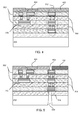
- FIG. 4 illustrates formation of a passivation layer and front-side contact pad in the die shown in FIG. 3 .
- An additional passivation layer 402 is formed over the metal wiring layers.
- the passivation layer 402 is a non-reactive surface film, such as an oxide or a nitride, that inhibits corrosion of the wiring layers 302.
- a front-side contact pad 404 is formed in the passivation layer 402. As described above, some applications may use the front side contact pad of the die configuration shown in FIG. 4 . In other applications, post-fabrication processes may further configure the die to implement one or more backside contacts.
- FIGs. 5 and 6 illustrate post-fabrication configuration of the reconfigurable semiconductor shown in FIG. 4 .
- the die may be reconfigured to implement a TSV, as shown in FIG. 1 , that can electrically couple a front-side contact to a back-side contact pad.
- Through silicon vias can be difficult to implement because etching often requires etching through several different materials. Because different materials etch at different rates, side walls of the etched via trench can be uneven. As a result, deposition of conductive and/or isolative materials in the via can be difficult. The uneven shape may also adversely affect electrical properties of the via such as inductance and capacitance. Deposition of conductive material in a TSV is also difficult due to higher aspect ratio of height to width in comparison to standard vias. The formation of a TSV entails deep etching through the majority of a die, forming a dielectric oxide layer along the sides of the TSV, and filling or plating of the TSV with a conductive material.
- a through silicon via may be implemented post-fabrication with the formation of a via through the passivation layer and a via through the substrate.
- FIG. 5 illustrates formation of vias on the front and back-sides of the die shown in FIG. 4 allowing access to the via stack 312.
- a first via 502 is formed in the passivation layer and a second via 504 is formed through the silicon substrate 202.
- FIG. 6 illustrates filling of the vias 502 and 504 and reconfiguration of the die to connect the circuit 310 to a back-side contact 606.
- an insulating material may be deposited to isolate the TSV from the substrate.
- a back-side contact is formed on the back-side of the die.
- the back-side contact is electrically coupled to via stack 312 through plated via 502.
- Post fabrication wiring 610 is formed over the passivation layer to electrically couple the back-side contact 606 to the circuit 310 through vias 502 and 504, via stack 312, and front-side contact 404.
- some embodiments may form a second passivation layer 608 on the backside of the substrate 202.
- a third passivation layer (not shown) may also be formed over the wire 610 and front-side contact 404 to prevent corrosion.
- the back-side via through the substrate 202 may be formed using a variety of via formation methods.
- vias 502 and 504 are illustrated as having a taper angle close to 90 degrees and being completely filled with conductive metal.
- other vias may be metal plated and/or tapered at other angles.
- FIGs. 7 and 8 illustrate a second method for formation of a back-side via and contact connected to the stacked via of FIG. 4 .
- FIG. 7 illustrates the formation of a conically shaped tapered via trench in substrate 202.
- FIG. 8 illustrates plating of the conically shaped tapered via. Because of the surface area of the conically shaped via, the via 702 may be plated with a thin metal plating 802. A passivation layer 804 is formed over the via plating 802. A back-side contact pad 806 is formed in the passivation layer and is electrically coupled to the metal plating 802.
Landscapes
- Internal Circuitry In Semiconductor Integrated Circuit Devices (AREA)
- Semiconductor Integrated Circuits (AREA)
- Engineering & Computer Science (AREA)
- Manufacturing & Machinery (AREA)
Abstract
Description
- One of the major trends in the semiconductor packaging industry is to use surface-mount technology (SMT) as a replacement for conventional plated-through-hole (PTH) technology. SMT offers several distinct advantages over PTH technology, such as greater packaging density, higher lead counts with shorter interconnection lengths and easier automation. Since SMT requires electronic devices and components to be mountable on the surface of a printed circuit board (PCB) or substrate, the materials and structure of traditional through-hole components including capacitors, resistors, and inductors have to be redesigned to meet the modern-day demand for short, thin, light, and small electronic devices. Examples of semiconductor devices accomplishing these objects include quad-flat, non-leaded packages. Quad-flat, non-leaded packages have a package structure in which space-consuming outer leads protruding laterally out of a package are eliminated. Instead, external electrode pads, which are to eventually be electrically connected to a circuit board, are provided on the bottom surface of the quad-flat, non-leaded package. The bottom surface of the package that connects to the circuit board may be referred to as the back-side of the package as used herein.
- Depending on the packaging and stacking of semiconductor dice for an application, it may be more desirable to implement a die with either front-side or back-side contacts. Ultimately, it may be necessary to implement different die layouts with different contacts for several applications. However, fabricating different die layouts for different packages and/or applications increases production complexity and costs.
- Aspects of the invention are defined in the accompanying claims.
- One or more embodiments may address one or more of the above issues.
- In one embodiment, a semiconductor is provided comprising a substrate and a plurality of wiring layers and dielectric layers formed on the substrate, the wiring layers implementing a circuit. The dielectric layers separate adjacent ones of the plurality of wiring layers. A first passivation layer is formed on the plurality of wiring layers. A first contact pad is formed in the passivation layer and electrically coupled to the circuit. A wire is formed on the passivation layer and connected to the contact pad. A through silicon via (TSV) is formed through the substrate, the plurality of wiring and dielectric layers, and the passivation layer. The TSV is electrically connected to the wire formed on the passivation layer. The TSV is electrically isolated from the wiring layers except for the connection provided by the metal wire formed on the passivation layer.
- In another embodiment, a method of forming a plurality of semiconductors is provided. A plurality of identical semiconductor dice is formed. Each die includes a substrate and a plurality of wiring layers and dielectric layers. The dielectric layers separate adjacent ones of the wiring layers and the wiring layers implement a circuit. A passivation layer is formed on the plurality of wiring layers. A front-side contact pad is formed in the passivation layer and electrically coupled to the circuit. A via stack is formed through the plurality of wiring and dielectric layers, the via stack is electrically isolated from the circuit implemented by the wiring layers. For each of a first subset of the plurality of identical semiconductor dice including at least one die, the circuit is left electrically isolated from the via stack. For each of a second subset of the plurality of identical semiconductor dice, the second subset is mutually exclusive from the first subset and includes at least one die, a back-side contact is formed. The back-side contact is formed by forming a first via through the passivation layer and electrically coupled to the via stack, forming a wire on the passivation layer to electrically couple the front-side contact pad to the first via, and forming a second via extending from a back-side of the substrate and through the substrate.
- In yet another embodiment, a method of forming a semiconductor with a back-side contact is provided. A semiconductor die including a substrate and a plurality of wiring layers and dielectric layers is formed. The dielectric layers separate adjacent ones of the wiring layers, and the wiring layers implement a circuit. A passivation layer is formed on the plurality of wiring layers. A front-side contact pad is formed in the passivation layer and electrically coupled to the circuit. A via stack is formed through the plurality of wiring and dielectric layers. The via stack is electrically isolated from the circuit implemented by the wiring layers. The die is reconfigured to have a back-side contact by performing the steps including: forming a first via through the passivation layer. The first via is electrically coupled to the via stack. A wire electrically coupling the front-side contact pad to the first via is formed on the passivation layer. A second via electrically coupled to the via stack is formed. The second via extends from a back-side of the substrate and through the substrate.
- The above discussion is not intended to describe each embodiment or every implementation. Various example embodiments may be more completely understood in consideration of the following detailed description in connection with the accompanying drawings, in which:
-
FIG. 1 shows a semiconductor reconfigured in post-fabrication processing to have a back-side contact; -
FIGs. 2 through 4 illustrate the fabrication of a reconfigurable semiconductor; -
FIGs. 5 and6 illustrate post-fabrication reconfiguration of the reconfigurable semiconductor shown inFIG. 4 ; and -
FIGs. 7 and 8 illustrate a second method for formation of a back-side via and contact connected to the stacked via. - While the disclosure is amenable to various modifications and alternative forms, examples thereof have been shown by way of example in the drawings and will be described in detail. It should be understood, however, that the intention is not to limit the disclosure to the particular embodiments shown and/or described. On the contrary, the intention is to cover all modifications, equivalents, and alternatives falling within the scope of the disclosure.
- In one or more embodiments, a semiconductor die is provided that may be easily reconfigured, via post fabrication processes, to implement back-side contacts. Such capability allows a batch of identical semiconductor dice to be used for a wider variety of applications. Some of the dice may be used in packages in which front-side contacts are used, and others of the dice may be used in packages in which the back-side contacts are used. Due to this increase versatility and simplified fabrication, manufacturing costs can be reduced and various combinations of different integrated circuit dice can be combined, e.g., for fast prototyping.
- In one embodiment, a die having one or more front-side contacts may be reconfigured to use back-side contacts.
FIG. 1 shows a semiconductor reconfigured in post-fabrication processing to have a back-side contact. A plurality ofwiring layers 104 anddielectric layers 106 are formed on asubstrate layer 102. Thedielectric layers 106 separate adjacent ones of the plurality ofwiring layers 104. A number of stacked vias and metal plates together implement a through silicon via (TSV) 112 passing through thewiring 104, dielectric 106, andsubstrate 102 layers. The wiring layers are patterned to implement acircuit 110 coupled to a front-side contact pad 114 and a portion of the TSV. - Prior to post-fabrication configuration, the die may be used in a number of applications which use the front-side contact pad. In such applications, the
TSV 112 remains electrically isolated from thecircuit 110. To configure the die to have a back-side contact, awire 122 is formed over thepassivation layer 120 to couple theTSV 112 to the front-side contact. As a result, a path is formed between thecircuit 110 and the back-side of the die. -
FIGs. 2-4 illustrate the fabrication of a reconfigurable semiconductor.FIG. 2 shows asubstrate 202 anddielectric isolation layer 204 on which metal semiconductor circuits may be formed.FIG. 3 illustrates formation of a plurality ofwiring layers 302 anddielectric layers 304 on the silicon substrate and dielectric shown inFIG. 2 . Thedielectric layers 304 separate adjacent ones of the plurality of wiring layers 310. The wiring layers are patterned to implement at least onecircuit 310 and at least one viastack 312 that are electrically isolated from each other. - The via stack is implemented by forming a
metal plate 320 in each of the wiring layers. The metal plates of adjacent wiring layers are vertically aligned and electrically connected to each other by means ofvias 322 formed in the dielectric layer that separates the adjacent wiring layers. The metal plate size within the metal layers can be designed with respect to metal tiling design rules. The metal plate size within the metal layers can be minimized with respect to the required sheet resistance. The size and distribution ofmetal vias 322 can be designed with respect to metal tiling design rules and electrical requirements. -
FIG. 4 illustrates formation of a passivation layer and front-side contact pad in the die shown inFIG. 3 . Anadditional passivation layer 402 is formed over the metal wiring layers. Thepassivation layer 402 is a non-reactive surface film, such as an oxide or a nitride, that inhibits corrosion of the wiring layers 302. To provide an external contact for the circuit, a front-side contact pad 404 is formed in thepassivation layer 402. As described above, some applications may use the front side contact pad of the die configuration shown inFIG. 4 . In other applications, post-fabrication processes may further configure the die to implement one or more backside contacts. -
FIGs. 5 and6 illustrate post-fabrication configuration of the reconfigurable semiconductor shown inFIG. 4 . The die may be reconfigured to implement a TSV, as shown inFIG. 1 , that can electrically couple a front-side contact to a back-side contact pad. - Through silicon vias can be difficult to implement because etching often requires etching through several different materials. Because different materials etch at different rates, side walls of the etched via trench can be uneven. As a result, deposition of conductive and/or isolative materials in the via can be difficult. The uneven shape may also adversely affect electrical properties of the via such as inductance and capacitance. Deposition of conductive material in a TSV is also difficult due to higher aspect ratio of height to width in comparison to standard vias. The formation of a TSV entails deep etching through the majority of a die, forming a dielectric oxide layer along the sides of the TSV, and filling or plating of the TSV with a conductive material. However, at high aspect ratios, current methods of via formation may cause oxide or metal plating of the via to form significantly faster at the top of the via than at the bottom. In addition to non-uniformity caused by the uneven deposition rates, the rapid growth at the top of the TSV may cause voids to become trapped in the TSV. Such variation and defects may be avoided by implementing the TSV with the via
stack 322 because the via stack is formed using a number of smaller vias which have a smaller aspect ratio. - By configuration the wiring layers to implement the via
stack 312 during fabrication of the circuit, a through silicon via may be implemented post-fabrication with the formation of a via through the passivation layer and a via through the substrate. -
FIG. 5 illustrates formation of vias on the front and back-sides of the die shown inFIG. 4 allowing access to the viastack 312. A first via 502 is formed in the passivation layer and a second via 504 is formed through thesilicon substrate 202. -
FIG. 6 illustrates filling of thevias circuit 310 to a back-side contact 606. In some embodiments, an insulating material may be deposited to isolate the TSV from the substrate. After vias 502 and 504 are filled or plated, a back-side contact is formed on the back-side of the die. The back-side contact is electrically coupled to viastack 312 through plated via 502.Post fabrication wiring 610 is formed over the passivation layer to electrically couple the back-side contact 606 to thecircuit 310 throughvias stack 312, and front-side contact 404. After reconfiguration, some embodiments may form asecond passivation layer 608 on the backside of thesubstrate 202. A third passivation layer (not shown) may also be formed over thewire 610 and front-side contact 404 to prevent corrosion. - It is recognized that the back-side via through the
substrate 202 may be formed using a variety of via formation methods. InFIG. 6 ,vias FIGs. 7 and 8 illustrate a second method for formation of a back-side via and contact connected to the stacked via ofFIG. 4 . -
FIG. 7 illustrates the formation of a conically shaped tapered via trench insubstrate 202.
FIG. 8 illustrates plating of the conically shaped tapered via. Because of the surface area of the conically shaped via, the via 702 may be plated with athin metal plating 802. Apassivation layer 804 is formed over the via plating 802. A back-side contact pad 806 is formed in the passivation layer and is electrically coupled to themetal plating 802. - Based upon the above discussion and illustrations, those skilled in the art will readily recognize that various modifications and changes may be made without strictly following the exemplary embodiments and applications illustrated and described herein. Such modifications do not depart from the scope of the present disclosure, including that set forth in the following claims.
Claims (15)
- A semiconductor comprising
a substrate;
a plurality of wiring layers and dielectric layers formed on the substrate, the dielectric layers separating adjacent ones of the plurality of wiring layers, and the wiring layers implementing a circuit;
a first passivation layer formed on the plurality of wiring layers;
a first contact pad formed in the passivation layer and electrically coupled to the circuit;
a wire formed on the passivation layer and connected to the contact pad; and
a through silicon via (TSV) formed through the substrate, the plurality of wiring and dielectric layers, and the passivation layer, the TSV electrically connected to the wire formed on the passivation layer, and the TSV being electrically isolated from the wiring layers except for the connection provided by the metal wire formed on the passivation layer. - The semiconductor of claim 1, further comprising a second contact pad formed below the substrate and electrically coupled to the TSV.
- The semiconductor of claim 1 or claim 2, wherein the TSV includes:a metal plate formed in each of the plurality of wiring layers; anda respective via through each dielectric layer separating adjacent ones of the plurality of wiring layers, each via connecting the metal plates in adjacent ones of the plurality of wiring layers.
- The semiconductor of claim 3, wherein the TSV further includes, a via formed through the substrate and electrically coupled to the metal plate formed in a bottom one of the plurality of wiring layers.
- The semiconductor of claim 4, wherein the via formed through the substrate and electrically coupled to the metal plate formed in a bottom one of the plurality of wiring layers is conical.
- The semiconductor of any preceding claim, further comprising a second passivation layer formed over the metal contact pad and over the wire formed on the first passivation layer.
- The semiconductor of any preceding claim, wherein the TSV formed through the substrate is electrically isolated from the substrate.
- A method of forming a plurality of semiconductors, the method comprising:forming a plurality of identical semiconductor dice, each die including:a substrate;a plurality of wiring layers and dielectric layers, the dielectric layers separating adjacent ones of the wiring layers, and the wiring layers implementing a circuit;a passivation layer formed on the plurality of wiring layers;a front-side contact pad formed in the passivation layer and electrically coupled to the circuit; anda via stack formed through the plurality of wiring and dielectric layers, the via stack electrically isolated from the circuit implemented by the wiring layers; andfor each of a first subset of the plurality of identical semiconductor dice including at least one die, leaving the circuit electrically isolated from the via stack; andfor each of a second subset of the plurality of identical semiconductor dice, the second subset being mutually exclusive from the first subset and including at least one die, forming a back-side contact by performing the steps including:forming a first via through the passivation layer and electrically coupled to the via stack;forming a wire on the passivation layer, the wire electrically coupling the front-side contact pad to the first via; andforming a second via extending from a back-side of the substrate and through the substrate, the second via electrically coupled to the via stack.
- A method of forming a semiconductor with a back-side contact, the method comprising:forming a semiconductor die including:a substrate;a plurality of wiring layers and dielectric layers, the dielectric layers separating adjacent ones of the wiring layers, and the wiring layers implementing a circuit;a passivation layer formed on the plurality of wiring layers;a front-side contact pad formed in the passivation layer and electrically coupled to the circuit; anda via stack formed through the plurality of wiring and dielectric layers, the via stack electrically isolated from the circuit implemented by the wiring layers; and reconfiguring the die to have a back-side contact by performing the steps including:forming a first via through the passivation layer and electrically coupled to the via stack;forming a wire on the passivation layer, the wire electrically coupling the front-side contact pad to the first via; andforming a second via extending from a back-side of the substrate and through the substrate, the second via electrically coupled to the via stack.
- The method of claim 8, further comprising, for each die in the second subset, forming a second passivation layer over the front-side contact pad and over the wire formed on top of the passivation layer of the at least one of the dice.
- The method of claim 8, further comprising, for each die in the second subset, forming a back-side contact pad on a back-side of the substrate of the at least one of the dice, the contact pad electrically coupled to the second via.
- The method of claim 11, further comprising:packaging each die of the first subset in a respective first semiconductor package, the first semiconductor package having an external contact wirebonded to the front-side contact pad; andpackaging each die of the second subset in a respective second semiconductor package, the second semiconductor package having an external contact wirebonded to the back-side contact pad.
- The method of claim 9, further comprising, forming a second passivation layer over the front-side contact pad and over the wire formed on top of the passivation layer of the at least one of the dice.
- The method of claim 9, further comprising forming a back-side contact pad electrically coupled to the second via on a back-side of the substrate of the die.
- The method of any of claims 8 to 14, wherein the via stack formed through the plurality of wiring and dielectric layers is electrically isolated from the substrate.
Applications Claiming Priority (1)
| Application Number | Priority Date | Filing Date | Title |
|---|---|---|---|
| US13/159,852 US8551882B2 (en) | 2011-06-14 | 2011-06-14 | Back-side contact formation |
Publications (2)
| Publication Number | Publication Date |
|---|---|
| EP2535925A1 true EP2535925A1 (en) | 2012-12-19 |
| EP2535925B1 EP2535925B1 (en) | 2019-02-06 |
Family
ID=46582526
Family Applications (1)
| Application Number | Title | Priority Date | Filing Date |
|---|---|---|---|
| EP12170469.6A Active EP2535925B1 (en) | 2011-06-14 | 2012-06-01 | Back-side contact formation |
Country Status (3)
| Country | Link |
|---|---|
| US (2) | US8551882B2 (en) |
| EP (1) | EP2535925B1 (en) |
| CN (1) | CN102832192B (en) |
Families Citing this family (8)
| Publication number | Priority date | Publication date | Assignee | Title |
|---|---|---|---|---|
| US9161461B2 (en) * | 2012-06-14 | 2015-10-13 | Zhuhai Advanced Chip Carriers & Electronic Substrate Solutions Technologies Co. Ltd. | Multilayer electronic structure with stepped holes |
| TWI496256B (en) * | 2012-12-28 | 2015-08-11 | 財團法人工業技術研究院 | Biaxial perforation bidirectional repair circuit for semiconductor device |
| US8912091B2 (en) | 2013-01-10 | 2014-12-16 | International Business Machines Corporation | Backside metal ground plane with improved metal adhesion and design structures |
| US9123789B2 (en) * | 2013-01-23 | 2015-09-01 | United Microelectronics Corp. | Chip with through silicon via electrode and method of forming the same |
| KR102320821B1 (en) | 2014-09-11 | 2021-11-02 | 삼성전자주식회사 | Semiconductor package |
| US20170061992A1 (en) * | 2015-08-31 | 2017-03-02 | HGST Netherlands B.V. | Multi-layer studs for advanced magnetic heads and high head density wafers |
| US9892970B2 (en) | 2016-06-02 | 2018-02-13 | Globalfoundries Inc. | Integrated circuit structure having deep trench capacitor and through-silicon via and method of forming same |
| US9929085B2 (en) | 2016-06-02 | 2018-03-27 | Globalfoundries Inc. | Integrated circuit structure having deep trench capacitor and through-silicon via and method of forming same |
Citations (5)
| Publication number | Priority date | Publication date | Assignee | Title |
|---|---|---|---|---|
| US20090014888A1 (en) * | 2007-07-12 | 2009-01-15 | Min-Hyung Lee | Semiconductor chip, method of fabricating the same and stack package having the same |
| US20090020842A1 (en) * | 2007-07-16 | 2009-01-22 | Taiwan Semiconductor Manufacturing Company, Ltd. | Embedded bonding pad for backside illuminated image sensor |
| US20100182041A1 (en) * | 2009-01-22 | 2010-07-22 | International Business Machines Corporation | 3d chip-stack with fuse-type through silicon via |
| US20110068456A1 (en) * | 2009-09-24 | 2011-03-24 | Headway Technologies, Inc. | Layered chip package and method of manufacturing same |
| US20110084385A1 (en) * | 2009-10-09 | 2011-04-14 | Elpida Memeory, Inc. | Semiconductor device and information processing system including the same |
Family Cites Families (3)
| Publication number | Priority date | Publication date | Assignee | Title |
|---|---|---|---|---|
| US6960837B2 (en) | 2002-02-26 | 2005-11-01 | International Business Machines Corporation | Method of connecting core I/O pins to backside chip I/O pads |
| JP3925378B2 (en) * | 2002-09-30 | 2007-06-06 | ソニー株式会社 | A method for manufacturing a high-frequency module device. |
| JP2007087975A (en) * | 2005-09-16 | 2007-04-05 | Ricoh Co Ltd | Semiconductor device |
-
2011
- 2011-06-14 US US13/159,852 patent/US8551882B2/en active Active
-
2012
- 2012-06-01 EP EP12170469.6A patent/EP2535925B1/en active Active
- 2012-06-11 CN CN201210190856.0A patent/CN102832192B/en active Active
-
2013
- 2013-08-07 US US13/961,129 patent/US8860230B2/en active Active
Patent Citations (5)
| Publication number | Priority date | Publication date | Assignee | Title |
|---|---|---|---|---|
| US20090014888A1 (en) * | 2007-07-12 | 2009-01-15 | Min-Hyung Lee | Semiconductor chip, method of fabricating the same and stack package having the same |
| US20090020842A1 (en) * | 2007-07-16 | 2009-01-22 | Taiwan Semiconductor Manufacturing Company, Ltd. | Embedded bonding pad for backside illuminated image sensor |
| US20100182041A1 (en) * | 2009-01-22 | 2010-07-22 | International Business Machines Corporation | 3d chip-stack with fuse-type through silicon via |
| US20110068456A1 (en) * | 2009-09-24 | 2011-03-24 | Headway Technologies, Inc. | Layered chip package and method of manufacturing same |
| US20110084385A1 (en) * | 2009-10-09 | 2011-04-14 | Elpida Memeory, Inc. | Semiconductor device and information processing system including the same |
Also Published As
| Publication number | Publication date |
|---|---|
| CN102832192B (en) | 2015-03-25 |
| EP2535925B1 (en) | 2019-02-06 |
| US20130320506A1 (en) | 2013-12-05 |
| US20120319250A1 (en) | 2012-12-20 |
| CN102832192A (en) | 2012-12-19 |
| US8551882B2 (en) | 2013-10-08 |
| US8860230B2 (en) | 2014-10-14 |
Similar Documents
| Publication | Publication Date | Title |
|---|---|---|
| US8860230B2 (en) | Back-side contact formation | |
| US12009289B2 (en) | Semiconductor package and manufacturing method thereof | |
| US9318465B2 (en) | Methods for forming a semiconductor device package | |
| US9721920B2 (en) | Embedded chip packages and methods for manufacturing an embedded chip package | |
| US8937389B2 (en) | Semiconductor devices comprising GSG interconnect structures | |
| CN104882417B (en) | Integrating passive Flip-Chip Using | |
| KR101107858B1 (en) | A conductive filler structure for a semiconductor substrate and a method of manufacturing the same | |
| CN110060982B (en) | Capacitor for interposer and method of making the same | |
| CN104916623B (en) | Semiconductor package and method of manufacturing semiconductor package substrate | |
| TW201630008A (en) | Polymer frame for chips having at least one through hole in series with a capacitor | |
| CN114946023A (en) | Integrated inductor with stacked metal lines | |
| CN106935563A (en) | Electronic package and its manufacturing method and substrate structure | |
| CN101312181B (en) | semiconductor chip, integrated circuit structure and semiconductor wafer | |
| CN102790030B (en) | Semiconductor structure having offset passivation to reduce electromigration | |
| CN105575915A (en) | Packaging structure and its manufacturing method | |
| CN112397497A (en) | Semiconductor package | |
| US20250079282A1 (en) | Packages with notched, interdigitated, and retracted metal layers | |
| CN115719738B (en) | substrate structure | |
| CN117727721A (en) | Wafer-based molded flip-chip routable IC packages | |
| US20180122721A1 (en) | Plug structure of a semiconductor chip and method of manufacturing the same | |
| TWI615933B (en) | Semiconductor device and method of manufacturing same | |
| TWI858603B (en) | Semiconductor device and forming method of semiconductor package | |
| US20250349768A1 (en) | Module containing fan-out wafer-level packaging unit connected to electronic by wire bonding | |
| US20250372562A1 (en) | Fan-out wafer-level packaging unit | |
| CN115621213A (en) | Semiconductor package structure and method for forming the same |
Legal Events
| Date | Code | Title | Description |
|---|---|---|---|
| PUAI | Public reference made under article 153(3) epc to a published international application that has entered the european phase |
Free format text: ORIGINAL CODE: 0009012 |
|
| AK | Designated contracting states |
Kind code of ref document: A1 Designated state(s): AL AT BE BG CH CY CZ DE DK EE ES FI FR GB GR HR HU IE IS IT LI LT LU LV MC MK MT NL NO PL PT RO RS SE SI SK SM TR |
|
| AX | Request for extension of the european patent |
Extension state: BA ME |
|
| 17P | Request for examination filed |
Effective date: 20130619 |
|
| RBV | Designated contracting states (corrected) |
Designated state(s): AL AT BE BG CH CY CZ DE DK EE ES FI FR GB GR HR HU IE IS IT LI LT LU LV MC MK MT NL NO PL PT RO RS SE SI SK SM TR |
|
| GRAP | Despatch of communication of intention to grant a patent |
Free format text: ORIGINAL CODE: EPIDOSNIGR1 |
|
| STAA | Information on the status of an ep patent application or granted ep patent |
Free format text: STATUS: GRANT OF PATENT IS INTENDED |
|
| INTG | Intention to grant announced |
Effective date: 20180925 |
|
| GRAS | Grant fee paid |
Free format text: ORIGINAL CODE: EPIDOSNIGR3 |
|
| GRAA | (expected) grant |
Free format text: ORIGINAL CODE: 0009210 |
|
| STAA | Information on the status of an ep patent application or granted ep patent |
Free format text: STATUS: THE PATENT HAS BEEN GRANTED |
|
| AK | Designated contracting states |
Kind code of ref document: B1 Designated state(s): AL AT BE BG CH CY CZ DE DK EE ES FI FR GB GR HR HU IE IS IT LI LT LU LV MC MK MT NL NO PL PT RO RS SE SI SK SM TR |
|
| REG | Reference to a national code |
Ref country code: GB Ref legal event code: FG4D |
|
| REG | Reference to a national code |
Ref country code: CH Ref legal event code: EP Ref country code: AT Ref legal event code: REF Ref document number: 1095418 Country of ref document: AT Kind code of ref document: T Effective date: 20190215 |
|
| REG | Reference to a national code |
Ref country code: IE Ref legal event code: FG4D |
|
| REG | Reference to a national code |
Ref country code: DE Ref legal event code: R096 Ref document number: 602012056428 Country of ref document: DE |
|
| REG | Reference to a national code |
Ref country code: NL Ref legal event code: MP Effective date: 20190206 |
|
| REG | Reference to a national code |
Ref country code: LT Ref legal event code: MG4D |
|
| PG25 | Lapsed in a contracting state [announced via postgrant information from national office to epo] |
Ref country code: NL Free format text: LAPSE BECAUSE OF FAILURE TO SUBMIT A TRANSLATION OF THE DESCRIPTION OR TO PAY THE FEE WITHIN THE PRESCRIBED TIME-LIMIT Effective date: 20190206 Ref country code: LT Free format text: LAPSE BECAUSE OF FAILURE TO SUBMIT A TRANSLATION OF THE DESCRIPTION OR TO PAY THE FEE WITHIN THE PRESCRIBED TIME-LIMIT Effective date: 20190206 Ref country code: FI Free format text: LAPSE BECAUSE OF FAILURE TO SUBMIT A TRANSLATION OF THE DESCRIPTION OR TO PAY THE FEE WITHIN THE PRESCRIBED TIME-LIMIT Effective date: 20190206 Ref country code: PT Free format text: LAPSE BECAUSE OF FAILURE TO SUBMIT A TRANSLATION OF THE DESCRIPTION OR TO PAY THE FEE WITHIN THE PRESCRIBED TIME-LIMIT Effective date: 20190606 Ref country code: NO Free format text: LAPSE BECAUSE OF FAILURE TO SUBMIT A TRANSLATION OF THE DESCRIPTION OR TO PAY THE FEE WITHIN THE PRESCRIBED TIME-LIMIT Effective date: 20190506 Ref country code: SE Free format text: LAPSE BECAUSE OF FAILURE TO SUBMIT A TRANSLATION OF THE DESCRIPTION OR TO PAY THE FEE WITHIN THE PRESCRIBED TIME-LIMIT Effective date: 20190206 |
|
| REG | Reference to a national code |
Ref country code: AT Ref legal event code: MK05 Ref document number: 1095418 Country of ref document: AT Kind code of ref document: T Effective date: 20190206 |
|
| PG25 | Lapsed in a contracting state [announced via postgrant information from national office to epo] |
Ref country code: HR Free format text: LAPSE BECAUSE OF FAILURE TO SUBMIT A TRANSLATION OF THE DESCRIPTION OR TO PAY THE FEE WITHIN THE PRESCRIBED TIME-LIMIT Effective date: 20190206 Ref country code: RS Free format text: LAPSE BECAUSE OF FAILURE TO SUBMIT A TRANSLATION OF THE DESCRIPTION OR TO PAY THE FEE WITHIN THE PRESCRIBED TIME-LIMIT Effective date: 20190206 Ref country code: BG Free format text: LAPSE BECAUSE OF FAILURE TO SUBMIT A TRANSLATION OF THE DESCRIPTION OR TO PAY THE FEE WITHIN THE PRESCRIBED TIME-LIMIT Effective date: 20190506 Ref country code: GR Free format text: LAPSE BECAUSE OF FAILURE TO SUBMIT A TRANSLATION OF THE DESCRIPTION OR TO PAY THE FEE WITHIN THE PRESCRIBED TIME-LIMIT Effective date: 20190507 Ref country code: IS Free format text: LAPSE BECAUSE OF FAILURE TO SUBMIT A TRANSLATION OF THE DESCRIPTION OR TO PAY THE FEE WITHIN THE PRESCRIBED TIME-LIMIT Effective date: 20190606 Ref country code: LV Free format text: LAPSE BECAUSE OF FAILURE TO SUBMIT A TRANSLATION OF THE DESCRIPTION OR TO PAY THE FEE WITHIN THE PRESCRIBED TIME-LIMIT Effective date: 20190206 |
|
| PG25 | Lapsed in a contracting state [announced via postgrant information from national office to epo] |
Ref country code: SK Free format text: LAPSE BECAUSE OF FAILURE TO SUBMIT A TRANSLATION OF THE DESCRIPTION OR TO PAY THE FEE WITHIN THE PRESCRIBED TIME-LIMIT Effective date: 20190206 Ref country code: EE Free format text: LAPSE BECAUSE OF FAILURE TO SUBMIT A TRANSLATION OF THE DESCRIPTION OR TO PAY THE FEE WITHIN THE PRESCRIBED TIME-LIMIT Effective date: 20190206 Ref country code: RO Free format text: LAPSE BECAUSE OF FAILURE TO SUBMIT A TRANSLATION OF THE DESCRIPTION OR TO PAY THE FEE WITHIN THE PRESCRIBED TIME-LIMIT Effective date: 20190206 Ref country code: CZ Free format text: LAPSE BECAUSE OF FAILURE TO SUBMIT A TRANSLATION OF THE DESCRIPTION OR TO PAY THE FEE WITHIN THE PRESCRIBED TIME-LIMIT Effective date: 20190206 Ref country code: ES Free format text: LAPSE BECAUSE OF FAILURE TO SUBMIT A TRANSLATION OF THE DESCRIPTION OR TO PAY THE FEE WITHIN THE PRESCRIBED TIME-LIMIT Effective date: 20190206 Ref country code: AL Free format text: LAPSE BECAUSE OF FAILURE TO SUBMIT A TRANSLATION OF THE DESCRIPTION OR TO PAY THE FEE WITHIN THE PRESCRIBED TIME-LIMIT Effective date: 20190206 Ref country code: DK Free format text: LAPSE BECAUSE OF FAILURE TO SUBMIT A TRANSLATION OF THE DESCRIPTION OR TO PAY THE FEE WITHIN THE PRESCRIBED TIME-LIMIT Effective date: 20190206 Ref country code: IT Free format text: LAPSE BECAUSE OF FAILURE TO SUBMIT A TRANSLATION OF THE DESCRIPTION OR TO PAY THE FEE WITHIN THE PRESCRIBED TIME-LIMIT Effective date: 20190206 |
|
| REG | Reference to a national code |
Ref country code: DE Ref legal event code: R097 Ref document number: 602012056428 Country of ref document: DE |
|
| PG25 | Lapsed in a contracting state [announced via postgrant information from national office to epo] |
Ref country code: PL Free format text: LAPSE BECAUSE OF FAILURE TO SUBMIT A TRANSLATION OF THE DESCRIPTION OR TO PAY THE FEE WITHIN THE PRESCRIBED TIME-LIMIT Effective date: 20190206 Ref country code: SM Free format text: LAPSE BECAUSE OF FAILURE TO SUBMIT A TRANSLATION OF THE DESCRIPTION OR TO PAY THE FEE WITHIN THE PRESCRIBED TIME-LIMIT Effective date: 20190206 |
|
| PLBE | No opposition filed within time limit |
Free format text: ORIGINAL CODE: 0009261 |
|
| STAA | Information on the status of an ep patent application or granted ep patent |
Free format text: STATUS: NO OPPOSITION FILED WITHIN TIME LIMIT |
|
| PG25 | Lapsed in a contracting state [announced via postgrant information from national office to epo] |
Ref country code: AT Free format text: LAPSE BECAUSE OF FAILURE TO SUBMIT A TRANSLATION OF THE DESCRIPTION OR TO PAY THE FEE WITHIN THE PRESCRIBED TIME-LIMIT Effective date: 20190206 |
|
| 26N | No opposition filed |
Effective date: 20191107 |
|
| PG25 | Lapsed in a contracting state [announced via postgrant information from national office to epo] |
Ref country code: MC Free format text: LAPSE BECAUSE OF FAILURE TO SUBMIT A TRANSLATION OF THE DESCRIPTION OR TO PAY THE FEE WITHIN THE PRESCRIBED TIME-LIMIT Effective date: 20190206 |
|
| REG | Reference to a national code |
Ref country code: CH Ref legal event code: PL |
|
| GBPC | Gb: european patent ceased through non-payment of renewal fee |
Effective date: 20190601 |
|
| PG25 | Lapsed in a contracting state [announced via postgrant information from national office to epo] |
Ref country code: SI Free format text: LAPSE BECAUSE OF FAILURE TO SUBMIT A TRANSLATION OF THE DESCRIPTION OR TO PAY THE FEE WITHIN THE PRESCRIBED TIME-LIMIT Effective date: 20190206 |
|
| REG | Reference to a national code |
Ref country code: BE Ref legal event code: MM Effective date: 20190630 |
|
| PG25 | Lapsed in a contracting state [announced via postgrant information from national office to epo] |
Ref country code: TR Free format text: LAPSE BECAUSE OF FAILURE TO SUBMIT A TRANSLATION OF THE DESCRIPTION OR TO PAY THE FEE WITHIN THE PRESCRIBED TIME-LIMIT Effective date: 20190206 |
|
| PG25 | Lapsed in a contracting state [announced via postgrant information from national office to epo] |
Ref country code: IE Free format text: LAPSE BECAUSE OF NON-PAYMENT OF DUE FEES Effective date: 20190601 Ref country code: GB Free format text: LAPSE BECAUSE OF NON-PAYMENT OF DUE FEES Effective date: 20190601 |
|
| PG25 | Lapsed in a contracting state [announced via postgrant information from national office to epo] |
Ref country code: LI Free format text: LAPSE BECAUSE OF NON-PAYMENT OF DUE FEES Effective date: 20190630 Ref country code: CH Free format text: LAPSE BECAUSE OF NON-PAYMENT OF DUE FEES Effective date: 20190630 Ref country code: BE Free format text: LAPSE BECAUSE OF NON-PAYMENT OF DUE FEES Effective date: 20190630 Ref country code: LU Free format text: LAPSE BECAUSE OF NON-PAYMENT OF DUE FEES Effective date: 20190601 |
|
| PG25 | Lapsed in a contracting state [announced via postgrant information from national office to epo] |
Ref country code: FR Free format text: LAPSE BECAUSE OF NON-PAYMENT OF DUE FEES Effective date: 20190630 |
|
| PG25 | Lapsed in a contracting state [announced via postgrant information from national office to epo] |
Ref country code: CY Free format text: LAPSE BECAUSE OF FAILURE TO SUBMIT A TRANSLATION OF THE DESCRIPTION OR TO PAY THE FEE WITHIN THE PRESCRIBED TIME-LIMIT Effective date: 20190206 |
|
| PG25 | Lapsed in a contracting state [announced via postgrant information from national office to epo] |
Ref country code: HU Free format text: LAPSE BECAUSE OF FAILURE TO SUBMIT A TRANSLATION OF THE DESCRIPTION OR TO PAY THE FEE WITHIN THE PRESCRIBED TIME-LIMIT; INVALID AB INITIO Effective date: 20120601 Ref country code: MT Free format text: LAPSE BECAUSE OF FAILURE TO SUBMIT A TRANSLATION OF THE DESCRIPTION OR TO PAY THE FEE WITHIN THE PRESCRIBED TIME-LIMIT Effective date: 20190206 |
|
| PG25 | Lapsed in a contracting state [announced via postgrant information from national office to epo] |
Ref country code: MK Free format text: LAPSE BECAUSE OF FAILURE TO SUBMIT A TRANSLATION OF THE DESCRIPTION OR TO PAY THE FEE WITHIN THE PRESCRIBED TIME-LIMIT Effective date: 20190206 |
|
| P01 | Opt-out of the competence of the unified patent court (upc) registered |
Effective date: 20230517 |
|
| PGFP | Annual fee paid to national office [announced via postgrant information from national office to epo] |
Ref country code: DE Payment date: 20250520 Year of fee payment: 14 |
|
| REG | Reference to a national code |
Ref country code: DE Ref legal event code: R079 Ref document number: 602012056428 Country of ref document: DE Free format text: PREVIOUS MAIN CLASS: H01L0021768000 Ipc: H10W0020000000 |