EP2533410A2 - High yield AC - AC power converter and method therefor - Google Patents
High yield AC - AC power converter and method therefor Download PDFInfo
- Publication number
- EP2533410A2 EP2533410A2 EP12171090A EP12171090A EP2533410A2 EP 2533410 A2 EP2533410 A2 EP 2533410A2 EP 12171090 A EP12171090 A EP 12171090A EP 12171090 A EP12171090 A EP 12171090A EP 2533410 A2 EP2533410 A2 EP 2533410A2
- Authority
- EP
- European Patent Office
- Prior art keywords
- signal
- bridge
- processor
- coupled
- output
- Prior art date
- Legal status (The legal status is an assumption and is not a legal conclusion. Google has not performed a legal analysis and makes no representation as to the accuracy of the status listed.)
- Granted
Links
Images



Classifications
-
- H—ELECTRICITY
- H02—GENERATION; CONVERSION OR DISTRIBUTION OF ELECTRIC POWER
- H02M—APPARATUS FOR CONVERSION BETWEEN AC AND AC, BETWEEN AC AND DC, OR BETWEEN DC AND DC, AND FOR USE WITH MAINS OR SIMILAR POWER SUPPLY SYSTEMS; CONVERSION OF DC OR AC INPUT POWER INTO SURGE OUTPUT POWER; CONTROL OR REGULATION THEREOF
- H02M5/00—Conversion of AC power input into AC power output, e.g. for change of voltage, for change of frequency, for change of number of phases
- H02M5/40—Conversion of AC power input into AC power output, e.g. for change of voltage, for change of frequency, for change of number of phases with intermediate conversion into DC
- H02M5/42—Conversion of AC power input into AC power output, e.g. for change of voltage, for change of frequency, for change of number of phases with intermediate conversion into DC by static converters
- H02M5/44—Conversion of AC power input into AC power output, e.g. for change of voltage, for change of frequency, for change of number of phases with intermediate conversion into DC by static converters using discharge tubes or semiconductor devices to convert the intermediate DC into AC
- H02M5/453—Conversion of AC power input into AC power output, e.g. for change of voltage, for change of frequency, for change of number of phases with intermediate conversion into DC by static converters using discharge tubes or semiconductor devices to convert the intermediate DC into AC using devices of a triode or transistor type requiring continuous application of a control signal
- H02M5/458—Conversion of AC power input into AC power output, e.g. for change of voltage, for change of frequency, for change of number of phases with intermediate conversion into DC by static converters using discharge tubes or semiconductor devices to convert the intermediate DC into AC using devices of a triode or transistor type requiring continuous application of a control signal using semiconductor devices only
- H02M5/4585—Conversion of AC power input into AC power output, e.g. for change of voltage, for change of frequency, for change of number of phases with intermediate conversion into DC by static converters using discharge tubes or semiconductor devices to convert the intermediate DC into AC using devices of a triode or transistor type requiring continuous application of a control signal using semiconductor devices only having a rectifier with controlled elements
-
- H—ELECTRICITY
- H02—GENERATION; CONVERSION OR DISTRIBUTION OF ELECTRIC POWER
- H02M—APPARATUS FOR CONVERSION BETWEEN AC AND AC, BETWEEN AC AND DC, OR BETWEEN DC AND DC, AND FOR USE WITH MAINS OR SIMILAR POWER SUPPLY SYSTEMS; CONVERSION OF DC OR AC INPUT POWER INTO SURGE OUTPUT POWER; CONTROL OR REGULATION THEREOF
- H02M5/00—Conversion of AC power input into AC power output, e.g. for change of voltage, for change of frequency, for change of number of phases
- H02M5/40—Conversion of AC power input into AC power output, e.g. for change of voltage, for change of frequency, for change of number of phases with intermediate conversion into DC
- H02M5/42—Conversion of AC power input into AC power output, e.g. for change of voltage, for change of frequency, for change of number of phases with intermediate conversion into DC by static converters
- H02M5/44—Conversion of AC power input into AC power output, e.g. for change of voltage, for change of frequency, for change of number of phases with intermediate conversion into DC by static converters using discharge tubes or semiconductor devices to convert the intermediate DC into AC
- H02M5/443—Conversion of AC power input into AC power output, e.g. for change of voltage, for change of frequency, for change of number of phases with intermediate conversion into DC by static converters using discharge tubes or semiconductor devices to convert the intermediate DC into AC using devices of a thyratron or thyristor type requiring extinguishing means
- H02M5/45—Conversion of AC power input into AC power output, e.g. for change of voltage, for change of frequency, for change of number of phases with intermediate conversion into DC by static converters using discharge tubes or semiconductor devices to convert the intermediate DC into AC using devices of a thyratron or thyristor type requiring extinguishing means using semiconductor devices only
- H02M5/452—Conversion of AC power input into AC power output, e.g. for change of voltage, for change of frequency, for change of number of phases with intermediate conversion into DC by static converters using discharge tubes or semiconductor devices to convert the intermediate DC into AC using devices of a thyratron or thyristor type requiring extinguishing means using semiconductor devices only with automatic control of output waveform
Definitions
- Embodiments of this disclosure relate generally to power converters, and more particularly, to an Alternating Current (AC) to AC power converter that does not require a Direct Current (DC) link or storage devices.
- AC Alternating Current
- DC Direct Current
- Wind turbines and flywheels are types of renewable energy devices that output variable frequency, variable voltage, AC electric power. Therefore, power converters may be used to convert the variable-frequency, variable-voltage, AC electric power to fixed-frequency, fixed-voltage, AC power.
- Wind turbine power systems spend a lot of time operating at light loads or fractions of their rated power capacities.
- These variable frequency drives typically employ dc voltage or current links for power distribution between the input and output converters and as a means to temporarily store energy.
- conventional power converters convert the generated AC power to DC power then to the required AC power.
- this method renders a low yield conversion.
- Standard, state-of-the-art, power converters are designed to operate most efficiently at full power all, or nearly all, of the time. Therefore, when wind turbine-driven generators are operating in low wind, light load, conditions, standard power converters are inefficient.
- An AC to AC power converter may have a rectifier configured to receive an AC signal.
- An H-Bridge may be coupled to the rectifier.
- a processor may be coupled to the rectifier and to the H-Bridge, wherein the processor may be configured to produce a pulse to modulate a rectified DC input to the H-Bridge.
- a wave filter may be coupled to the H-Bridge and configured to modulate an output of the H-Bridge to an AC voltage of a desired frequency, wherein an output of the wave filter may be coupled to the processor.
- An AC to AC power converter may have a rectifier configured to receive an AC signal.
- An H-Bridge may be coupled to the rectifier.
- a DC filter may be coupled to the rectifier and the H-Bridge.
- a processor may be coupled to the rectifier and to the H-Bridge, wherein the processor is configured to produce a pulse to modulate a rectified DC input to the H-Bridge.
- An H-Bridge driver may be coupled to the H-Bridge and the processor.
- a sine wave filter may be coupled to the H-Bridge and configured to modulate an output of the H-Bridge to an AC voltage of a desired frequency, wherein an output of the wave filter may be coupled to the processor.
- a method for converting AC power may include receiving an input AC signal, converting the input AC signal into a full wave rectified signal, producing a pulse to modulate the full wave rectified signal, sending the modulated full wave rectified signal to an H-Bridge, filtering an output signal of the H-Bridge to an AC voltage signal of a desired frequency.
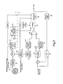
- an AC-to-AC power conversion system 10 (hereinafter system 10) is shown.
- the system 10 may provide direct AC-AC power conversion without a DC link or storage devices that produces a high efficiency conversion.
- the system 10 may convert variable-frequency, variable-voltage, AC electric power to fixed-frequency, fixed-voltage, AC power.
- the system 10 may receive an AC input (AC-In) via signal line 11.
- the AC input AC-In may be variable-frequency, variable-voltage, AC signal.
- the AC input AC-In may be a signal generated by a wind turbine, a flywheel or the like. The above is given as an example and should not be seen in a limiting manner.
- the AC input AC-In may be sent to an input power rectifier 12 (hereinafter rectifier 12).
- the rectifier 12 may be used to convert the AC input AC-In into a full wave rectified signal to one of constant polarity at its output. This may be done to extract a frequency content of the AC input AC-In for processing by a processor 16.
- the processor 16 is a Digital Signal Processor (DSP). However, this should not be seen in a limiting manner.
- DSP Digital Signal Processor
- the rectified signal from the rectifier 12 may have a peak voltage that is not compatible with the processor 16. Therefore, a step down transformer 18A may be used to lower the voltage level of the rectified signal to one compatible with the processor 16.
- the processor 16 may be used to produce a pulse to modulate the rectified signal from the rectifier 12 or the constant DC voltage(s) DC from the DC Filter 22 to an H-Bridge component 20.
- a device driver 14 may be used to allow the processor 16 to interact with the H-Bridge component 20.
- the device 14 may be a driver circuit or the like.
- the rectified DC signal DC may also be sent to a DC filter 22.
- the rectified DC signal DC may not be a steady signal.
- a DC filter 22 may be used to smooth the rectified DC signal DC to the H-Bridge component 20.
- the H-Bridge component 20 may enable a voltage to be applied across an output AC-Out in either direction.
- the output signal of the H-Bridge component 20 may be sent to a transformer 24.
- the transformer 24 maybe used to step down or to step up the peak voltages of the output of the H-Bridge component 20 to desired levels.
- the output of the transformer 24 may pass through a filter 26.
- the filter 26 may be used to produce a clean AC signal at the output AC-Out (See Figure 2).
- Figure 2 shows the output signal AC-Out from the system 10 for a specific input single AC-In on signal line 11.
- the filter 26 may be used to average the modulated voltages into an AC voltage signal of a desired frequency.
- the filter 26 is, for example, a 60Hz Sine Wave Filter.
- the filter 26 is a low pass filter that averages the modulated voltages into, for example, a 60 Hz AC voltage signal at the output AC-Out.
- the filter 26 may also be used to removes transients and noise at the output. The filter 26 makes sure that the system 10 is stable at varying loads.
- a feedback loop may be needed to control the AC voltage signal at the output AC-Out.
- the AC voltage signal at the output AC-Out may be sent back to the processor 16. Since the AC voltage signal at the output AC-Out may have a peak voltage that is not compatible with the processor 16, a step down transformer 28 may be used to lower the voltage level to one compatible with the processor 16.
- a reference sine wave generator 30 may send an output to the processor 16.
- the processor 16 may compare the frequency of the AC voltage signal at the output AC-Out to the output of the reference sine wave generator 30.
- the reference sine wave generator 30 may have a value of 60Hz.
- the processor 16 may then adjust the pulse signal used to modulate the rectified DC input to the H-Bridge component 20 and thus adjust the frequency of the AC voltage signal at the output AC-Out.
- the processor 16 may be used to stabilize the AC voltage signal at the output AC-Out for the AC-In signal which may be at varying frequencies.
- the processor 16 operates differently for transient inputs (TS) and for steady state and low frequency inputs (SS), i.e. less than 1 KHz.
- the TS AC conversion may be used to convert the transient or the first few cycles of the AC-In signal into the AC voltage signal of the desired frequency (for example, 60-Hz in the embodiment shown in Figure 1 ) .
- the AC-In signal may be sent to a step-down signal transformer 18B to interface the signal to the processor 16.
- the processor 16 may sample the signal and determines its periodic cycles. If the frequency is 1 KHz or above, for example, the processor 16 may derive a control signal to be used for carrier generation.
- the processor 16 may derive the density of full wave cycles or the rectified signal from the rectifier 12 to generate the desired output sine wave voltage.
- the processor 16 may utilizes the feedback from the AC voltage signal at the output AC-Out to add or subtract the density of the full wave cycles. Also, the processor 16 may sends a control signal to the filter 26 to select the ac-ac output topology.
- the AC-In signal may be a full wave rectified signal with plus/minus voltage V.
- the filter 22 may be used to produce constant DC voltages DC at the input of the H-Bridge component 20.
- the output of the rectifier 12 may be connected to a step-down signal transformer 18 to make the signal available to the processor 16.
- the processor 16 may sample the signal and determines its frequency. If the frequency is less than 1 KHz, for example) or if the rectifier is generating the +Vdc (SS), the processor 16 may derive a square wave signal for carrier generation. Also, the processor 16 may send a control signal to the filter 26 to select the ac-ac output topology to compensate for the input peak signal attenuation.
- the upper portion A depicted operation during the TS AC conversion process.
- the lower portion B depicts operation during the SS AC conversion process.
- a frequency qualifier 32 may be used to determine the frequency of the signal 33 from the step-down signal transformer 18. If the frequency of the signal from the step-down signal transformer 18 is greater than 1 KHz, for example, the signal may be sent to a boost topology 34.
- the boost topology 34 may be used to increase the voltage level of the signal at the output of the H-Bridge to a desired application.
- the signal may then be sent to a Pulse Density Modulator (PDM) generator 36.
- PDM Pulse Density Modulator
- the PDM generator 36 may be used to produce a pulse to modulate the rectified DC signal to the H-bridge 20 to generate the desired AC voltage signal at the output AC-Out.
- the PDM generator 36 may utilized a DSP processor to estimate the periodic cycle of the input to generate the clocking of the input through the H-Bridge AC interface.
- the output of a control clock may be continually synchronized with each input cycle.
- the DSP of the PDM generator 36 may use an adaptive PDM algorithm to adjust the pulse frequency of the control clock from the estimated amplitude, phase, and frequency of the referenced sine wave.
- the PDM generator 36 may have a feedback loop from the output AC-Out to add or subtract the density of the full wave cycles.
- a square wave signal may be produced for carrier generation.
- a signal from a bipolar half wave unit 40 may be sent to a square wave generator 42.
- An output of the square wave generator 42 may be coupled to an integrator carrier generator 44.
- the integrator carrier generator 44 may be the pulse width carrier modulator.
- input signals AC-In i.e., greater than 1KHz
- the integrated signal may be a continuation of pulses to control the number of AC cycles that generates the desired AC voltage signal at the output AC-Out.
- the integrated signal may be a continuation of ramp signals that may be used to modulate the output of the DC rectifier to generate the desired AC voltage signal at the output AC-Out.
- An output of the integrator carrier generator 44 may be sent to a comparator 46.
- the signal from the integrator carrier generator 44 is used as a reference for the comparator 46 to control the signal at the output AC-Out.
- a feedback loop may be formed back to the comparator 46.
- An output of the step down transformer 28 may be sent to a synchronizer 48.
- the synchronizer 48 may be used to synchronize the output of the step down transformer 28 with the sine wave reference signal.
- An error amplifier 50 may be used to generate the difference between the sine wave reference signal and the signal at the output AC-Out.
- a modified sine wave reference signal generator 52 may be used to generate a modified 60Hz reference signal, for example, which is sent to the comparator 46. Thus, if the amplitude of the signal at the output AC-Out is lower, the error generated may be positive to increase the output peak until it is equal or greater than the reference.
- the system 10 may provide a stabilized signal at the output AC-Out that may be equal to, for example, the 60Hz reference.
- the output of the error amplifier 50 may be the error between the example 60Hz Reference source and the signal at the output AC-Out.
- the output of the error amplifier 50 may be sent to a calibrating device 52 to adjust the signal at the output AC-Out.
- the PDM clock generator 54 may be used to clock the periodic input voltages through the H-Bridge 20 to generate the desired signal at the output AC-Out.
- the inverse of the clocks may be used to generate the SS rectified dc voltage. When the rectified DC voltage reaches steady-state; the system 10 transfers the mode of operation from TS to SS mode.
- the system 10 may provide direct AC-AC power conversion without a DC link or storage devices that produces a high efficiency conversion.
- the system 10 may provide a direct AC-AC power conversion principle that leads to the distinct conversion system with no dc-link energy storage components. This direct AC-AC conversion may be achieved by schemes that use pulse density modulation.
- the carrier signal may be derived from the periodic cycling of the input signal AC-In. Each cycle may be sampled by the processor 16 ( Figure 1 ) to supply the required energy to transform the input periodic cycle into the desired frequency at the output AC-Out (for example, 60-Hz as shown in Figure 5 ). This may be necessary for high speed modulation to null the effects of the RC time constant of the DC filter 22.
- the modulating signal may be synchronized with the input signal AC-In and the continuation of pulses to estimate a 60-Hz, ac output for example.
- the efficiency of this modulation scheme may be a function of the input frequency; the higher the frequency, the higher the efficiency of the ac-ac conversion. Also, the null cycles of the modulated signal may be used to clock the rest of the ac input cycles to the rectifier 12 ( Figure 1 ).
- the PWM scheme may utilize a voltage DC link to convert the AC output. This method may be used to maximize power efficiency by storing the input energy in the form of DC voltage conversion.
Landscapes
- Engineering & Computer Science (AREA)
- Power Engineering (AREA)
- Rectifiers (AREA)
- Ac-Ac Conversion (AREA)
- Inverter Devices (AREA)
- Dc-Dc Converters (AREA)
Abstract
Description
- Embodiments of this disclosure relate generally to power converters, and more particularly, to an Alternating Current (AC) to AC power converter that does not require a Direct Current (DC) link or storage devices.
- Wind turbines and flywheels are types of renewable energy devices that output variable frequency, variable voltage, AC electric power. Therefore, power converters may be used to convert the variable-frequency, variable-voltage, AC electric power to fixed-frequency, fixed-voltage, AC power.
- Wind turbine power systems spend a lot of time operating at light loads or fractions of their rated power capacities. These variable frequency drives typically employ dc voltage or current links for power distribution between the input and output converters and as a means to temporarily store energy. Thus, conventional power converters convert the generated AC power to DC power then to the required AC power. Unfortunately, this method renders a low yield conversion. Standard, state-of-the-art, power converters are designed to operate most efficiently at full power all, or nearly all, of the time. Therefore, when wind turbine-driven generators are operating in low wind, light load, conditions, standard power converters are inefficient.
- Therefore, it would be desirable to provide a system and method that overcomes the above problems.
- An AC to AC power converter may have a rectifier configured to receive an AC signal. An H-Bridge may be coupled to the rectifier. A processor may be coupled to the rectifier and to the H-Bridge, wherein the processor may be configured to produce a pulse to modulate a rectified DC input to the H-Bridge. A wave filter may be coupled to the H-Bridge and configured to modulate an output of the H-Bridge to an AC voltage of a desired frequency, wherein an output of the wave filter may be coupled to the processor.
- An AC to AC power converter may have a rectifier configured to receive an AC signal. An H-Bridge may be coupled to the rectifier. A DC filter may be coupled to the rectifier and the H-Bridge. A processor may be coupled to the rectifier and to the H-Bridge, wherein the processor is configured to produce a pulse to modulate a rectified DC input to the H-Bridge. An H-Bridge driver may be coupled to the H-Bridge and the processor. A sine wave filter may be coupled to the H-Bridge and configured to modulate an output of the H-Bridge to an AC voltage of a desired frequency, wherein an output of the wave filter may be coupled to the processor.
- A method for converting AC power, may include receiving an input AC signal, converting the input AC signal into a full wave rectified signal, producing a pulse to modulate the full wave rectified signal, sending the modulated full wave rectified signal to an H-Bridge, filtering an output signal of the H-Bridge to an AC voltage signal of a desired frequency. The features, functions, and advantages can be achieved independently in various embodiments of the disclosure or may be combined in yet other embodiments.
- Embodiments of the disclosure will become more fully understood from the detailed description and the accompanying drawings, wherein:
-
Figure 1 is a simplified block diagram of a high yield AC-AC Power conversion system; -
Figure 2 is a diagram showing the power conversion output of the system ofFigure 1 ; -
Figure 3 is a flow chart showing operation of a processor used inFigure 1 ; -
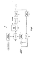
Figure 4 is a simplified block diagram of a Pulse Density Modulator (PDM) control signal generator used inFigure 3 ; -
Figure 5A depicts transient state PWM scheme to achieve direct AC-AC high efficient power conversion; and -
Figure 5B depicts a steady state modulation scheme PWM scheme to achieve direct AC-AC high efficient power conversion. - Referring to
Figure 1 , an AC-to-AC power conversion system 10 (hereinafter system 10) is shown. Thesystem 10 may provide direct AC-AC power conversion without a DC link or storage devices that produces a high efficiency conversion. Thesystem 10 may convert variable-frequency, variable-voltage, AC electric power to fixed-frequency, fixed-voltage, AC power. - The
system 10 may receive an AC input (AC-In) viasignal line 11. The AC input AC-In may be variable-frequency, variable-voltage, AC signal. The AC input AC-In may be a signal generated by a wind turbine, a flywheel or the like. The above is given as an example and should not be seen in a limiting manner. During steady state operation, the AC input AC-In may be sent to an input power rectifier 12 (hereinafter rectifier 12). Therectifier 12 may be used to convert the AC input AC-In into a full wave rectified signal to one of constant polarity at its output. This may be done to extract a frequency content of the AC input AC-In for processing by aprocessor 16. In the embodiment shown inFigure 1 , theprocessor 16 is a Digital Signal Processor (DSP). However, this should not be seen in a limiting manner. - The rectified signal from the
rectifier 12 may have a peak voltage that is not compatible with theprocessor 16. Therefore, a step downtransformer 18A may be used to lower the voltage level of the rectified signal to one compatible with theprocessor 16. - The
processor 16 may be used to produce a pulse to modulate the rectified signal from therectifier 12 or the constant DC voltage(s) DC from theDC Filter 22 to an H-Bridge component 20. Adevice driver 14 may be used to allow theprocessor 16 to interact with the H-Bridge component 20. Thedevice 14 may be a driver circuit or the like. - As shown in
Figure 1 , the rectified DC signal DC may also be sent to aDC filter 22. The rectified DC signal DC may not be a steady signal. Thus, aDC filter 22 may be used to smooth the rectified DC signal DC to the H-Bridge component 20. The H-Bridge component 20 may enable a voltage to be applied across an output AC-Out in either direction. - The output signal of the H-
Bridge component 20 may be sent to atransformer 24. Thetransformer 24 maybe used to step down or to step up the peak voltages of the output of the H-Bridge component 20 to desired levels. The output of thetransformer 24 may pass through afilter 26. Thefilter 26 may be used to produce a clean AC signal at the output AC-Out (SeeFigure 2). Figure 2 shows the output signal AC-Out from thesystem 10 for a specific input single AC-In onsignal line 11. Thefilter 26 may be used to average the modulated voltages into an AC voltage signal of a desired frequency. In the embodiment ofFigure 1 , thefilter 26 is, for example, a 60Hz Sine Wave Filter. Thefilter 26 is a low pass filter that averages the modulated voltages into, for example, a 60 Hz AC voltage signal at the output AC-Out. Thefilter 26 may also be used to removes transients and noise at the output. Thefilter 26 makes sure that thesystem 10 is stable at varying loads. - A feedback loop may be needed to control the AC voltage signal at the output AC-Out. Thus, the AC voltage signal at the output AC-Out may be sent back to the
processor 16. Since the AC voltage signal at the output AC-Out may have a peak voltage that is not compatible with theprocessor 16, a step downtransformer 28 may be used to lower the voltage level to one compatible with theprocessor 16. - A reference
sine wave generator 30 may send an output to theprocessor 16. Theprocessor 16 may compare the frequency of the AC voltage signal at the output AC-Out to the output of the referencesine wave generator 30. The referencesine wave generator 30 may have a value of 60Hz. Theprocessor 16 may then adjust the pulse signal used to modulate the rectified DC input to the H-Bridge component 20 and thus adjust the frequency of the AC voltage signal at the output AC-Out. - The
processor 16 may be used to stabilize the AC voltage signal at the output AC-Out for the AC-In signal which may be at varying frequencies. Theprocessor 16 operates differently for transient inputs (TS) and for steady state and low frequency inputs (SS), i.e. less than 1 KHz. - The TS AC conversion may be used to convert the transient or the first few cycles of the AC-In signal into the AC voltage signal of the desired frequency (for example, 60-Hz in the embodiment shown in
Figure 1 ) . The AC-In signal may be sent to a step-downsignal transformer 18B to interface the signal to theprocessor 16. Theprocessor 16 may sample the signal and determines its periodic cycles. If the frequency is 1 KHz or above, for example, theprocessor 16 may derive a control signal to be used for carrier generation. Theprocessor 16 may derive the density of full wave cycles or the rectified signal from therectifier 12 to generate the desired output sine wave voltage. Theprocessor 16 may utilizes the feedback from the AC voltage signal at the output AC-Out to add or subtract the density of the full wave cycles. Also, theprocessor 16 may sends a control signal to thefilter 26 to select the ac-ac output topology. - In the low frequency AC conversion, the AC-In signal may be a full wave rectified signal with plus/minus voltage V. The
filter 22 may be used to produce constant DC voltages DC at the input of the H-Bridge component 20. The output of therectifier 12 may be connected to a step-down signal transformer 18 to make the signal available to theprocessor 16. Theprocessor 16 may sample the signal and determines its frequency. If the frequency is less than 1 KHz, for example) or if the rectifier is generating the +Vdc (SS), theprocessor 16 may derive a square wave signal for carrier generation. Also, theprocessor 16 may send a control signal to thefilter 26 to select the ac-ac output topology to compensate for the input peak signal attenuation. - Referring now to
Figure 3 , operation of theprocessor 16 can be described. The upper portion A depicted operation during the TS AC conversion process. The lower portion B depicts operation during the SS AC conversion process. - A
frequency qualifier 32 may be used to determine the frequency of thesignal 33 from the step-down signal transformer 18. If the frequency of the signal from the step-down signal transformer 18 is greater than 1 KHz, for example, the signal may be sent to aboost topology 34. Theboost topology 34 may be used to increase the voltage level of the signal at the output of the H-Bridge to a desired application. The signal may then be sent to a Pulse Density Modulator (PDM)generator 36. - The
PDM generator 36 may be used to produce a pulse to modulate the rectified DC signal to the H-bridge 20 to generate the desired AC voltage signal at the output AC-Out. ThePDM generator 36 may utilized a DSP processor to estimate the periodic cycle of the input to generate the clocking of the input through the H-Bridge AC interface. The output of a control clock may be continually synchronized with each input cycle. The DSP of thePDM generator 36 may use an adaptive PDM algorithm to adjust the pulse frequency of the control clock from the estimated amplitude, phase, and frequency of the referenced sine wave. ThePDM generator 36 may have a feedback loop from the output AC-Out to add or subtract the density of the full wave cycles. - If the input frequency of the signal from the step-down signal transformer 18 is less than 1 KHz, for example, a square wave signal may be produced for carrier generation. In
Figure 3 , a signal from a bipolar half wave unit 40 may be sent to a square wave generator 42. An output of the square wave generator 42 may be coupled to an integrator carrier generator 44. The integrator carrier generator 44 may be the pulse width carrier modulator. At high frequencies input signals AC-In (i.e., greater than 1KHz), the integrated signal may be a continuation of pulses to control the number of AC cycles that generates the desired AC voltage signal at the output AC-Out. At low frequency input signals AC-In, the integrated signal may be a continuation of ramp signals that may be used to modulate the output of the DC rectifier to generate the desired AC voltage signal at the output AC-Out. An output of the integrator carrier generator 44 may be sent to acomparator 46. The signal from the integrator carrier generator 44 is used as a reference for thecomparator 46 to control the signal at the output AC-Out. - A feedback loop may be formed back to the
comparator 46. An output of the step downtransformer 28 may be sent to a synchronizer 48. The synchronizer 48 may be used to synchronize the output of the step downtransformer 28 with the sine wave reference signal. Anerror amplifier 50 may be used to generate the difference between the sine wave reference signal and the signal at the output AC-Out. A modified sine wave reference signal generator 52 may be used to generate a modified 60Hz reference signal, for example, which is sent to thecomparator 46. Thus, if the amplitude of the signal at the output AC-Out is lower, the error generated may be positive to increase the output peak until it is equal or greater than the reference. If the signal at the output AC-Out is greater, then the error generated may be negative to lower the amplitude of the signal at the output AC-Out until it is equal or lower than the example 60Hz reference. Thus, thesystem 10 may provide a stabilized signal at the output AC-Out that may be equal to, for example, the 60Hz reference. - Referring now to
Figure 4 , an example of a block diagram of the PDMcontrol signal generator 36 is shown. The output of theerror amplifier 50 may be the error between the example 60Hz Reference source and the signal at the output AC-Out. The output of theerror amplifier 50 may be sent to a calibrating device 52 to adjust the signal at the output AC-Out. ThePDM clock generator 54 may be used to clock the periodic input voltages through the H-Bridge 20 to generate the desired signal at the output AC-Out. The inverse of the clocks may be used to generate the SS rectified dc voltage. When the rectified DC voltage reaches steady-state; thesystem 10 transfers the mode of operation from TS to SS mode. - The
system 10 may provide direct AC-AC power conversion without a DC link or storage devices that produces a high efficiency conversion. Thesystem 10 may provide a direct AC-AC power conversion principle that leads to the distinct conversion system with no dc-link energy storage components. This direct AC-AC conversion may be achieved by schemes that use pulse density modulation. - Referring now to
Figure 5 , two modulation schemes may be utilized. In a High Speed Modulation, for the 1st few milliseconds after null, the carrier signal may be derived from the periodic cycling of the input signal AC-In. Each cycle may be sampled by the processor 16 (Figure 1 ) to supply the required energy to transform the input periodic cycle into the desired frequency at the output AC-Out (for example, 60-Hz as shown inFigure 5 ). This may be necessary for high speed modulation to null the effects of the RC time constant of theDC filter 22. As shown inFigure 5 , the modulating signal may be synchronized with the input signal AC-In and the continuation of pulses to estimate a 60-Hz, ac output for example. The efficiency of this modulation scheme may be a function of the input frequency; the higher the frequency, the higher the efficiency of the ac-ac conversion. Also, the null cycles of the modulated signal may be used to clock the rest of the ac input cycles to the rectifier 12 (Figure 1 ). - In Steady-State Modulation (
Figure 5b ), after a few milliseconds when the Vdc has stabilized, traditional PWM scheme may be implemented. The PWM scheme may utilize a voltage DC link to convert the AC output. This method may be used to maximize power efficiency by storing the input energy in the form of DC voltage conversion. - While embodiments of the disclosure have been described in terms of various specific embodiments, those skilled in the art will recognize that the embodiments of the disclosure can be practiced with modifications within the spirit and scope of the claims.
- The present invention discloses subject matter in accordance with the following numbered clauses:
-
Clause 1. An AC to AC power converter comprising:- a
rectifier 12 configured to receive anAC signal source 11; - an H-
Bridge 20 coupled to the rectifier; - a
processor 16 coupled to therectifier 12 and to the H-Bridge, wherein theprocessor 16 is configured to produce a pulse to modulate a rectified DC input to the H-Bridge; and - a
wave filter 26 coupled to the H-Bridge 20 configured to modulate an output of the H-Bridge to an AC voltage of a desired frequency, wherein an output of the wave filter is coupled to theprocessor 16.
- a
-
Clause 2. An AC to AC power converter in accordance withClause 1, further comprising a DC filter coupled to the rectifier and the H-Bridge. - Clause 3. An AC to AC power converter in accordance with
Clause 1 orClause 2, further comprising a high frequency transformer coupled to the H-bridge and the wave filter. - Clause 4. An AC to AC power converter in accordance with
Clause 1, further comprising an H-Bridge driver coupled to the H-Bridge and the processor. - Clause 5. An AC to AC power converter in accordance with
Clause 1, further comprising a first step down transformer coupled to the rectifier and the processor. - Clause 6. An AC to AC power converter in accordance with
Clause 1, further comprising a second step down transformer coupled to the wave filter and the processor. - Clause 7. An AC to AC power converter in accordance with
Clause 1, further comprising a reference wave signal coupled to the processor. - Clause 8. An AC to AC power converter in accordance with
Clause 1, wherein the wave filter is a 60Hz Sine wave filter. - Clause 9. An AC to AC power converter in accordance with Clause 7, wherein the reference wave signal is a 60Hz sine wave reference wave signal.
-
Clause 10. An AC to AC power converter comprising:- a rectifier configured to receive an AC signal;
- an H-Bridge coupled to the rectifier;
- a DC filter coupled to the rectifier and the H-Bridge;
- a processor coupled to the rectifier and to the H-Bridge, wherein the processor is configured to produce a pulse to modulate a rectified DC input to the H-Bridge;
- an H-Bridge driver coupled to the H-Bridge and the processor; and
- a sine wave filter coupled to the H-Bridge configured to modulate an output of the H-Bridge to an AC voltage of a desired frequency, wherein an output of the wave filter is coupled to the processor.
-
Clause 11. An AC to AC power converter in accordance withClause 10, further comprising a high frequency transformer coupled to the H-bridge and the sine wave filter. -
Clause 12. An AC to AC power converter in accordance withClause 10, further comprising a first step down transformer coupled to the rectifier and the processor. - Clause 13. An AC to AC power converter in accordance with
Clause 10, further comprising a second step down transformer coupled to the sine wave filter and the processor. -
Clause 14. An AC to AC power converter in accordance withClause 10, further comprising a reference wave signal coupled to the processor. - Clause 15. An AC to AC power converter in accordance with
Clause 10, wherein the sine wave filter is a 60Hz Sine wave filter. -
Clause 16. An AC to AC power converter in accordance withClause 14, wherein the reference wave signal is a 60Hz sine wave reference wave signal. - Clause 17. A method for converting AC power, comprising:
- receiving an input AC signal;
- converting the input AC signal into a full wave rectified signal;
- producing a pulse to modulate the full wave rectified signal;
- sending the modulated full wave rectified signal to an H-Bridge;
- sending the modulated full wave rectified signal to a DC Filter;
- filtering an output signal of the H-Bridge to an AC voltage signal of a desired frequency.
- Clause 18. The method of Clause 17, further comprising stepping down a frequency of the output signal of the H-Bridge to said desired frequency.
- Clause 19. The method of Clause 17, further comprising stepping down a voltage of the full wave rectified signal to form a carrier reference signal for a processor unit.
-
Clause 20. The method of Clause 19, further comprising forming a control loop between the AC voltage signal of a desired frequency and the processor unit. - Clause 21. The method of Clause 17, wherein receiving an input AC signal further comprises receiving the AC signal from a power generating device.
-
Clause 22. The method of Clause 17, wherein receiving an input AC signal further comprises receiving the AC signal from a power generating device, the AC signal being of variable frequency. - Nonetheless, for the avoidance of doubt, please note that the scope of the invention is to be defined by the appended claims.
Claims (13)
- An AC to AC power converter comprising:a rectifier 12 configured to receive an AC signal source 11;an H-Bridge 20 coupled to the rectifier;a processor 16 coupled to the rectifier 12 and to the H-Bridge, wherein the processor 16 is configured to produce a pulse to modulate a rectified DC input to the H-Bridge; anda wave filter 26 coupled to the H-Bridge 20 configured to modulate an output of the H-Bridge to an AC voltage of a desired frequency, wherein an output of the wave filter is coupled to the processor 16.
- An AC to AC power converter in accordance with Claim 1, further comprising a DC filter coupled to the rectifier and the H-Bridge.
- An AC to AC power converter in accordance with Claim 1 or Claim 2, further comprising a high frequency transformer coupled to the H-bridge and the wave filter.
- An AC to AC power converter in accordance with any of the preceding claims, further comprising an H-Bridge driver coupled to the H-Bridge and the processor.
- An AC to AC power converter in accordance with any of the preceding claims, further comprising a first step down transformer coupled to the rectifier and the processor.
- An AC to AC power converter in accordance with any of the preceding claims, further comprising a second step down transformer coupled to the wave filter and the processor.
- An AC to AC power converter in accordance with any of the preceding claims, further comprising a reference wave signal coupled to the processor.
- An AC to AC power converter in accordance with any of the preceding claims, wherein the wave filter is a 60Hz Sine wave filter.
- A method for converting AC power, comprising:receiving an input AC signal;converting the input AC signal into a full wave rectified signal;producing a pulse to modulate the full wave rectified signal;sending the modulated full wave rectified signal to an H-Bridge;sending the modulated full wave rectified signal to a DC Filter;filtering an output signal of the H-Bridge to an AC voltage signal of a desired frequency.
- The method of Claim 9, further comprising stepping down a frequency of the output signal of the H-Bridge to said desired frequency.
- The method of Claim 9 or Claim 10, further comprising stepping down a voltage of the full wave rectified signal to form a carrier reference signal for a processor unit and forming a control loop between the AC voltage signal of a desired frequency and the processor unit.
- The method of any of Claims 9 through 11, wherein receiving an input AC signal further comprises receiving the AC signal from a power generating device.
- The method of any of Claims 10 through 12, wherein receiving an input AC signal further comprises receiving the AC signal from a power generating device, the AC signal being of variable frequency.
Applications Claiming Priority (1)
| Application Number | Priority Date | Filing Date | Title |
|---|---|---|---|
| US13/156,254 US8559198B2 (en) | 2011-06-08 | 2011-06-08 | High yield AC-AC power converter and method therefor |
Publications (3)
| Publication Number | Publication Date |
|---|---|
| EP2533410A2 true EP2533410A2 (en) | 2012-12-12 |
| EP2533410A3 EP2533410A3 (en) | 2017-06-21 |
| EP2533410B1 EP2533410B1 (en) | 2020-12-30 |
Family
ID=46384144
Family Applications (1)
| Application Number | Title | Priority Date | Filing Date |
|---|---|---|---|
| EP12171090.9A Active EP2533410B1 (en) | 2011-06-08 | 2012-06-06 | High yield AC - AC power converter and method therefor |
Country Status (5)
| Country | Link |
|---|---|
| US (1) | US8559198B2 (en) |
| EP (1) | EP2533410B1 (en) |
| JP (1) | JP6122584B2 (en) |
| CN (1) | CN102820790B (en) |
| ES (1) | ES2861426T3 (en) |
Families Citing this family (3)
| Publication number | Priority date | Publication date | Assignee | Title |
|---|---|---|---|---|
| US10218277B2 (en) | 2016-02-22 | 2019-02-26 | The Boeing Company | Adaptable high efficiency power inverter system |
| CN108092741B (en) * | 2017-12-12 | 2021-03-19 | 深圳和而泰数据资源与云技术有限公司 | Communication method, terminal and communication device based on audio interface |
| CN109194148B (en) * | 2018-10-11 | 2020-12-29 | 中国兵器装备集团自动化研究所 | Novel high-precision high-power alternating current constant current source design method |
Family Cites Families (22)
| Publication number | Priority date | Publication date | Assignee | Title |
|---|---|---|---|---|
| US4443759A (en) * | 1981-05-07 | 1984-04-17 | Magnaflux Corporation | Magnetizing current supply for magnetic particle inspection with SCR's connected to three-phase secondary windings for rectification and control |
| JPS61280773A (en) * | 1985-06-03 | 1986-12-11 | Nippon Electric Ind Co Ltd | Pulse-width control type inverter |
| US5018058A (en) * | 1990-07-05 | 1991-05-21 | Power Management International, Inc. | High frequency AC voltage control |
| US5367448A (en) * | 1992-08-07 | 1994-11-22 | Carroll Lawrence B | Three phase AC to DC power converter |
| US5451962A (en) * | 1994-08-26 | 1995-09-19 | Martin Marietta Corporation | Boost regulated capacitor multiplier for pulse load |
| JPH09117162A (en) * | 1995-10-14 | 1997-05-02 | Shigehiro Imoto | Electric adjusting equipment |
| US6021052A (en) * | 1997-09-22 | 2000-02-01 | Statpower Technologies Partnership | DC/AC power converter |
| US6034489A (en) * | 1997-12-04 | 2000-03-07 | Matsushita Electric Works R&D Laboratory, Inc. | Electronic ballast circuit |
| CA2382358C (en) * | 2001-04-18 | 2007-01-09 | Gennum Corporation | Digital quasi-rms detector |
| US6608401B1 (en) * | 2002-02-15 | 2003-08-19 | Black & Decker Inc. | Alternator/inverter with dual H-bridge |
| US6838856B2 (en) * | 2002-10-04 | 2005-01-04 | Spx Corporation | Apparatus and method for high-frequency operation in a battery charger |
| WO2006121425A2 (en) * | 2005-05-05 | 2006-11-16 | Atlas Marine Systems, Lp | System and method for electrical power conversion |
| EP1920515A4 (en) * | 2005-08-30 | 2016-09-28 | Abb Research Ltd | REGULATION OF WIND POWER LOAD POWER RATE AND ENERGY CONVERTER |
| US7679941B2 (en) * | 2007-06-06 | 2010-03-16 | General Electric Company | Power conversion system with galvanically isolated high frequency link |
| JP2009033800A (en) * | 2007-07-24 | 2009-02-12 | Toyota Industries Corp | Bidirectional dc/ac inverter |
| US8796884B2 (en) * | 2008-12-20 | 2014-08-05 | Solarbridge Technologies, Inc. | Energy conversion systems with power control |
| JP2009159670A (en) * | 2007-12-25 | 2009-07-16 | Fdk Corp | Inverter device |
| US8279648B2 (en) * | 2008-03-20 | 2012-10-02 | Pratt & Whitney Canada Corp. | Power inverter and method |
| US8009449B2 (en) * | 2009-06-05 | 2011-08-30 | NPhysics, Inc | DC-to-AC power inverter and methods |
| US8427123B2 (en) * | 2009-07-08 | 2013-04-23 | Microchip Technology Incorporated | System, method and apparatus to transition between pulse width modulation and pulse-frequency modulation in a switch mode power supply |
| CN101626163B (en) * | 2009-08-04 | 2012-09-05 | 清华大学 | Hybrid wind power generation system |
| US8476859B2 (en) * | 2010-09-30 | 2013-07-02 | Rockwell Automation Technologies, Inc. | DC power for SGCT devices using a high frequency current loop with multiple current transformers |
-
2011
- 2011-06-08 US US13/156,254 patent/US8559198B2/en active Active
-
2012
- 2012-06-06 EP EP12171090.9A patent/EP2533410B1/en active Active
- 2012-06-06 JP JP2012129202A patent/JP6122584B2/en active Active
- 2012-06-06 ES ES12171090T patent/ES2861426T3/en active Active
- 2012-06-08 CN CN201210188800.1A patent/CN102820790B/en active Active
Non-Patent Citations (1)
| Title |
|---|
| None |
Also Published As
| Publication number | Publication date |
|---|---|
| CN102820790B (en) | 2016-08-03 |
| ES2861426T3 (en) | 2021-10-06 |
| EP2533410B1 (en) | 2020-12-30 |
| EP2533410A3 (en) | 2017-06-21 |
| CN102820790A (en) | 2012-12-12 |
| JP6122584B2 (en) | 2017-04-26 |
| US20120314460A1 (en) | 2012-12-13 |
| JP2012257449A (en) | 2012-12-27 |
| US8559198B2 (en) | 2013-10-15 |
Similar Documents
| Publication | Publication Date | Title |
|---|---|---|
| US8310102B2 (en) | System and method for power conversion | |
| CN108923462B (en) | Photovoltaic power generation system virtual synchronous machine control method, device, converter and system | |
| CN102545671A (en) | Power-generating system, power converter system and method of converting power | |
| TW200941897A (en) | Systems and methods for uninterruptible power supply control | |
| US10135352B2 (en) | Controller for power converter with frequency modulated carrier | |
| KR101920469B1 (en) | Grid connected single-stage inverter based on cuk converter | |
| CA2648793C (en) | Power inverter and method | |
| Tayebi et al. | Mitigation of current distortion in a three-phase microinverter with phase skipping using a synchronous sampling DC-link voltage control | |
| US8559198B2 (en) | High yield AC-AC power converter and method therefor | |
| US9887643B2 (en) | Bidirectional electrical signal converter | |
| Sevilmiş et al. | An experimental study of grid tied inverter for renewable energy systems | |
| Mo et al. | Active damping of oscillations in LC-filter for line connected, current controlled, PWM voltage source converters | |
| WO2026040800A1 (en) | Synchronization method for implementing grid connection of flyback microinverter by means of square-wave harmonic decomposition | |
| Mirzahosseini et al. | A lifetime improved single phase grid connected photovoltaic inverter | |
| Kumar et al. | SEPIC converter with 3-level NPC multi-level inverter for wind energy system (WES) | |
| Bortis et al. | 25-kW three-phase unity power factor buck–boost rectifier with wide input and output range for pulse load applications | |
| Tayebi et al. | Implementing synchronous DC link voltage control with phase skipping on a three-phase microinverter using minimum DC link capacitance | |
| CN112534703B (en) | System and method for generating a high frequency switching signal for a power converter | |
| JP2023516797A (en) | Power converter for photovoltaic energy sources | |
| Vijayalakshmi et al. | Design and development of controller for PMSG based wind energy conversion system | |
| JP2011193704A (en) | Dc-ac power converter | |
| KR100964080B1 (en) | Power conversion device and pulse width modulation control method in dual excitation induction wind power generator | |
| Salmon et al. | A hybrid current controller for a 1-phase PWM rectifier combining hysteresis and carrier-based schemes to achieve a zero current error and unipolar PWM waveforms | |
| Zabihi et al. | A high voltage power converter with a frequency and voltage controller | |
| Han et al. | Hybrid-mode Cuk inverter with low-voltage ride-through capability under grid-faults |
Legal Events
| Date | Code | Title | Description |
|---|---|---|---|
| PUAI | Public reference made under article 153(3) epc to a published international application that has entered the european phase |
Free format text: ORIGINAL CODE: 0009012 |
|
| 17P | Request for examination filed |
Effective date: 20120606 |
|
| AK | Designated contracting states |
Kind code of ref document: A2 Designated state(s): AL AT BE BG CH CY CZ DE DK EE ES FI FR GB GR HR HU IE IS IT LI LT LU LV MC MK MT NL NO PL PT RO RS SE SI SK SM TR |
|
| AX | Request for extension of the european patent |
Extension state: BA ME |
|
| PUAL | Search report despatched |
Free format text: ORIGINAL CODE: 0009013 |
|
| AK | Designated contracting states |
Kind code of ref document: A3 Designated state(s): AL AT BE BG CH CY CZ DE DK EE ES FI FR GB GR HR HU IE IS IT LI LT LU LV MC MK MT NL NO PL PT RO RS SE SI SK SM TR |
|
| AX | Request for extension of the european patent |
Extension state: BA ME |
|
| RIC1 | Information provided on ipc code assigned before grant |
Ipc: H02M 5/458 20060101AFI20170518BHEP |
|
| STAA | Information on the status of an ep patent application or granted ep patent |
Free format text: STATUS: EXAMINATION IS IN PROGRESS |
|
| 17Q | First examination report despatched |
Effective date: 20180308 |
|
| REG | Reference to a national code |
Ref country code: DE Ref legal event code: R079 Ref document number: 602012073916 Country of ref document: DE Free format text: PREVIOUS MAIN CLASS: H02M0005458000 Ipc: H02M0005040000 |
|
| GRAP | Despatch of communication of intention to grant a patent |
Free format text: ORIGINAL CODE: EPIDOSNIGR1 |
|
| STAA | Information on the status of an ep patent application or granted ep patent |
Free format text: STATUS: GRANT OF PATENT IS INTENDED |
|
| RIC1 | Information provided on ipc code assigned before grant |
Ipc: H02M 5/04 20060101AFI20200113BHEP |
|
| INTG | Intention to grant announced |
Effective date: 20200205 |
|
| GRAJ | Information related to disapproval of communication of intention to grant by the applicant or resumption of examination proceedings by the epo deleted |
Free format text: ORIGINAL CODE: EPIDOSDIGR1 |
|
| STAA | Information on the status of an ep patent application or granted ep patent |
Free format text: STATUS: EXAMINATION IS IN PROGRESS |
|
| INTC | Intention to grant announced (deleted) | ||
| GRAP | Despatch of communication of intention to grant a patent |
Free format text: ORIGINAL CODE: EPIDOSNIGR1 |
|
| STAA | Information on the status of an ep patent application or granted ep patent |
Free format text: STATUS: GRANT OF PATENT IS INTENDED |
|
| INTG | Intention to grant announced |
Effective date: 20200722 |
|
| GRAS | Grant fee paid |
Free format text: ORIGINAL CODE: EPIDOSNIGR3 |
|
| GRAA | (expected) grant |
Free format text: ORIGINAL CODE: 0009210 |
|
| STAA | Information on the status of an ep patent application or granted ep patent |
Free format text: STATUS: THE PATENT HAS BEEN GRANTED |
|
| AK | Designated contracting states |
Kind code of ref document: B1 Designated state(s): AL AT BE BG CH CY CZ DE DK EE ES FI FR GB GR HR HU IE IS IT LI LT LU LV MC MK MT NL NO PL PT RO RS SE SI SK SM TR |
|
| REG | Reference to a national code |
Ref country code: GB Ref legal event code: FG4D |
|
| REG | Reference to a national code |
Ref country code: AT Ref legal event code: REF Ref document number: 1350922 Country of ref document: AT Kind code of ref document: T Effective date: 20210115 |
|
| REG | Reference to a national code |
Ref country code: DE Ref legal event code: R096 Ref document number: 602012073916 Country of ref document: DE |
|
| REG | Reference to a national code |
Ref country code: IE Ref legal event code: FG4D |
|
| PG25 | Lapsed in a contracting state [announced via postgrant information from national office to epo] |
Ref country code: GR Free format text: LAPSE BECAUSE OF FAILURE TO SUBMIT A TRANSLATION OF THE DESCRIPTION OR TO PAY THE FEE WITHIN THE PRESCRIBED TIME-LIMIT Effective date: 20210331 Ref country code: RS Free format text: LAPSE BECAUSE OF FAILURE TO SUBMIT A TRANSLATION OF THE DESCRIPTION OR TO PAY THE FEE WITHIN THE PRESCRIBED TIME-LIMIT Effective date: 20201230 Ref country code: FI Free format text: LAPSE BECAUSE OF FAILURE TO SUBMIT A TRANSLATION OF THE DESCRIPTION OR TO PAY THE FEE WITHIN THE PRESCRIBED TIME-LIMIT Effective date: 20201230 Ref country code: NO Free format text: LAPSE BECAUSE OF FAILURE TO SUBMIT A TRANSLATION OF THE DESCRIPTION OR TO PAY THE FEE WITHIN THE PRESCRIBED TIME-LIMIT Effective date: 20210330 |
|
| REG | Reference to a national code |
Ref country code: AT Ref legal event code: MK05 Ref document number: 1350922 Country of ref document: AT Kind code of ref document: T Effective date: 20201230 |
|
| PG25 | Lapsed in a contracting state [announced via postgrant information from national office to epo] |
Ref country code: SE Free format text: LAPSE BECAUSE OF FAILURE TO SUBMIT A TRANSLATION OF THE DESCRIPTION OR TO PAY THE FEE WITHIN THE PRESCRIBED TIME-LIMIT Effective date: 20201230 Ref country code: LV Free format text: LAPSE BECAUSE OF FAILURE TO SUBMIT A TRANSLATION OF THE DESCRIPTION OR TO PAY THE FEE WITHIN THE PRESCRIBED TIME-LIMIT Effective date: 20201230 Ref country code: BG Free format text: LAPSE BECAUSE OF FAILURE TO SUBMIT A TRANSLATION OF THE DESCRIPTION OR TO PAY THE FEE WITHIN THE PRESCRIBED TIME-LIMIT Effective date: 20210330 |
|
| REG | Reference to a national code |
Ref country code: NL Ref legal event code: MP Effective date: 20201230 |
|
| PG25 | Lapsed in a contracting state [announced via postgrant information from national office to epo] |
Ref country code: HR Free format text: LAPSE BECAUSE OF FAILURE TO SUBMIT A TRANSLATION OF THE DESCRIPTION OR TO PAY THE FEE WITHIN THE PRESCRIBED TIME-LIMIT Effective date: 20201230 |
|
| REG | Reference to a national code |
Ref country code: LT Ref legal event code: MG9D |
|
| PG25 | Lapsed in a contracting state [announced via postgrant information from national office to epo] |
Ref country code: PT Free format text: LAPSE BECAUSE OF FAILURE TO SUBMIT A TRANSLATION OF THE DESCRIPTION OR TO PAY THE FEE WITHIN THE PRESCRIBED TIME-LIMIT Effective date: 20210430 Ref country code: RO Free format text: LAPSE BECAUSE OF FAILURE TO SUBMIT A TRANSLATION OF THE DESCRIPTION OR TO PAY THE FEE WITHIN THE PRESCRIBED TIME-LIMIT Effective date: 20201230 Ref country code: SK Free format text: LAPSE BECAUSE OF FAILURE TO SUBMIT A TRANSLATION OF THE DESCRIPTION OR TO PAY THE FEE WITHIN THE PRESCRIBED TIME-LIMIT Effective date: 20201230 Ref country code: LT Free format text: LAPSE BECAUSE OF FAILURE TO SUBMIT A TRANSLATION OF THE DESCRIPTION OR TO PAY THE FEE WITHIN THE PRESCRIBED TIME-LIMIT Effective date: 20201230 Ref country code: CZ Free format text: LAPSE BECAUSE OF FAILURE TO SUBMIT A TRANSLATION OF THE DESCRIPTION OR TO PAY THE FEE WITHIN THE PRESCRIBED TIME-LIMIT Effective date: 20201230 Ref country code: EE Free format text: LAPSE BECAUSE OF FAILURE TO SUBMIT A TRANSLATION OF THE DESCRIPTION OR TO PAY THE FEE WITHIN THE PRESCRIBED TIME-LIMIT Effective date: 20201230 Ref country code: NL Free format text: LAPSE BECAUSE OF FAILURE TO SUBMIT A TRANSLATION OF THE DESCRIPTION OR TO PAY THE FEE WITHIN THE PRESCRIBED TIME-LIMIT Effective date: 20201230 |
|
| PG25 | Lapsed in a contracting state [announced via postgrant information from national office to epo] |
Ref country code: PL Free format text: LAPSE BECAUSE OF FAILURE TO SUBMIT A TRANSLATION OF THE DESCRIPTION OR TO PAY THE FEE WITHIN THE PRESCRIBED TIME-LIMIT Effective date: 20201230 Ref country code: AT Free format text: LAPSE BECAUSE OF FAILURE TO SUBMIT A TRANSLATION OF THE DESCRIPTION OR TO PAY THE FEE WITHIN THE PRESCRIBED TIME-LIMIT Effective date: 20201230 |
|
| PG25 | Lapsed in a contracting state [announced via postgrant information from national office to epo] |
Ref country code: IS Free format text: LAPSE BECAUSE OF FAILURE TO SUBMIT A TRANSLATION OF THE DESCRIPTION OR TO PAY THE FEE WITHIN THE PRESCRIBED TIME-LIMIT Effective date: 20210430 |
|
| REG | Reference to a national code |
Ref country code: DE Ref legal event code: R097 Ref document number: 602012073916 Country of ref document: DE |
|
| REG | Reference to a national code |
Ref country code: ES Ref legal event code: FG2A Ref document number: 2861426 Country of ref document: ES Kind code of ref document: T3 Effective date: 20211006 |
|
| PG25 | Lapsed in a contracting state [announced via postgrant information from national office to epo] |
Ref country code: AL Free format text: LAPSE BECAUSE OF FAILURE TO SUBMIT A TRANSLATION OF THE DESCRIPTION OR TO PAY THE FEE WITHIN THE PRESCRIBED TIME-LIMIT Effective date: 20201230 Ref country code: IT Free format text: LAPSE BECAUSE OF FAILURE TO SUBMIT A TRANSLATION OF THE DESCRIPTION OR TO PAY THE FEE WITHIN THE PRESCRIBED TIME-LIMIT Effective date: 20201230 |
|
| PLBE | No opposition filed within time limit |
Free format text: ORIGINAL CODE: 0009261 |
|
| STAA | Information on the status of an ep patent application or granted ep patent |
Free format text: STATUS: NO OPPOSITION FILED WITHIN TIME LIMIT |
|
| PG25 | Lapsed in a contracting state [announced via postgrant information from national office to epo] |
Ref country code: DK Free format text: LAPSE BECAUSE OF FAILURE TO SUBMIT A TRANSLATION OF THE DESCRIPTION OR TO PAY THE FEE WITHIN THE PRESCRIBED TIME-LIMIT Effective date: 20201230 |
|
| 26N | No opposition filed |
Effective date: 20211001 |
|
| PG25 | Lapsed in a contracting state [announced via postgrant information from national office to epo] |
Ref country code: MC Free format text: LAPSE BECAUSE OF FAILURE TO SUBMIT A TRANSLATION OF THE DESCRIPTION OR TO PAY THE FEE WITHIN THE PRESCRIBED TIME-LIMIT Effective date: 20201230 |
|
| REG | Reference to a national code |
Ref country code: CH Ref legal event code: PL |
|
| PG25 | Lapsed in a contracting state [announced via postgrant information from national office to epo] |
Ref country code: SI Free format text: LAPSE BECAUSE OF FAILURE TO SUBMIT A TRANSLATION OF THE DESCRIPTION OR TO PAY THE FEE WITHIN THE PRESCRIBED TIME-LIMIT Effective date: 20201230 |
|
| REG | Reference to a national code |
Ref country code: BE Ref legal event code: MM Effective date: 20210630 |
|
| PG25 | Lapsed in a contracting state [announced via postgrant information from national office to epo] |
Ref country code: LU Free format text: LAPSE BECAUSE OF NON-PAYMENT OF DUE FEES Effective date: 20210606 |
|
| PG25 | Lapsed in a contracting state [announced via postgrant information from national office to epo] |
Ref country code: LI Free format text: LAPSE BECAUSE OF NON-PAYMENT OF DUE FEES Effective date: 20210630 Ref country code: IE Free format text: LAPSE BECAUSE OF NON-PAYMENT OF DUE FEES Effective date: 20210606 Ref country code: CH Free format text: LAPSE BECAUSE OF NON-PAYMENT OF DUE FEES Effective date: 20210630 |
|
| PG25 | Lapsed in a contracting state [announced via postgrant information from national office to epo] |
Ref country code: IS Free format text: LAPSE BECAUSE OF FAILURE TO SUBMIT A TRANSLATION OF THE DESCRIPTION OR TO PAY THE FEE WITHIN THE PRESCRIBED TIME-LIMIT Effective date: 20210430 |
|
| PG25 | Lapsed in a contracting state [announced via postgrant information from national office to epo] |
Ref country code: BE Free format text: LAPSE BECAUSE OF NON-PAYMENT OF DUE FEES Effective date: 20210630 |
|
| PG25 | Lapsed in a contracting state [announced via postgrant information from national office to epo] |
Ref country code: HU Free format text: LAPSE BECAUSE OF FAILURE TO SUBMIT A TRANSLATION OF THE DESCRIPTION OR TO PAY THE FEE WITHIN THE PRESCRIBED TIME-LIMIT; INVALID AB INITIO Effective date: 20120606 Ref country code: CY Free format text: LAPSE BECAUSE OF FAILURE TO SUBMIT A TRANSLATION OF THE DESCRIPTION OR TO PAY THE FEE WITHIN THE PRESCRIBED TIME-LIMIT Effective date: 20201230 |
|
| P01 | Opt-out of the competence of the unified patent court (upc) registered |
Effective date: 20230516 |
|
| PG25 | Lapsed in a contracting state [announced via postgrant information from national office to epo] |
Ref country code: SM Free format text: LAPSE BECAUSE OF FAILURE TO SUBMIT A TRANSLATION OF THE DESCRIPTION OR TO PAY THE FEE WITHIN THE PRESCRIBED TIME-LIMIT Effective date: 20201230 |
|
| PG25 | Lapsed in a contracting state [announced via postgrant information from national office to epo] |
Ref country code: MK Free format text: LAPSE BECAUSE OF FAILURE TO SUBMIT A TRANSLATION OF THE DESCRIPTION OR TO PAY THE FEE WITHIN THE PRESCRIBED TIME-LIMIT Effective date: 20201230 |
|
| PG25 | Lapsed in a contracting state [announced via postgrant information from national office to epo] |
Ref country code: TR Free format text: LAPSE BECAUSE OF FAILURE TO SUBMIT A TRANSLATION OF THE DESCRIPTION OR TO PAY THE FEE WITHIN THE PRESCRIBED TIME-LIMIT Effective date: 20201230 |
|
| PG25 | Lapsed in a contracting state [announced via postgrant information from national office to epo] |
Ref country code: MT Free format text: LAPSE BECAUSE OF FAILURE TO SUBMIT A TRANSLATION OF THE DESCRIPTION OR TO PAY THE FEE WITHIN THE PRESCRIBED TIME-LIMIT Effective date: 20201230 |
|
| PGFP | Annual fee paid to national office [announced via postgrant information from national office to epo] |
Ref country code: DE Payment date: 20250627 Year of fee payment: 14 |
|
| PGFP | Annual fee paid to national office [announced via postgrant information from national office to epo] |
Ref country code: GB Payment date: 20250627 Year of fee payment: 14 |
|
| PGFP | Annual fee paid to national office [announced via postgrant information from national office to epo] |
Ref country code: FR Payment date: 20250625 Year of fee payment: 14 |
|
| PGFP | Annual fee paid to national office [announced via postgrant information from national office to epo] |
Ref country code: ES Payment date: 20250701 Year of fee payment: 14 |