EP2533317A2 - Laminate structure, method for manufacturing a laminate structure, electronic element array, image displaying medium, image displaying apparatus, diamine, polyamic acid, and polyimide - Google Patents
Laminate structure, method for manufacturing a laminate structure, electronic element array, image displaying medium, image displaying apparatus, diamine, polyamic acid, and polyimide Download PDFInfo
- Publication number
- EP2533317A2 EP2533317A2 EP20120170848 EP12170848A EP2533317A2 EP 2533317 A2 EP2533317 A2 EP 2533317A2 EP 20120170848 EP20120170848 EP 20120170848 EP 12170848 A EP12170848 A EP 12170848A EP 2533317 A2 EP2533317 A2 EP 2533317A2
- Authority
- EP
- European Patent Office
- Prior art keywords
- polyimide
- diamine
- polyamic acid
- less
- laminate structure
- Prior art date
- Legal status (The legal status is an assumption and is not a legal conclusion. Google has not performed a legal analysis and makes no representation as to the accuracy of the status listed.)
- Withdrawn
Links
- 239000004642 Polyimide Substances 0.000 title claims abstract description 99
- 229920001721 polyimide Polymers 0.000 title claims abstract description 99
- 150000004985 diamines Chemical class 0.000 title claims abstract description 78
- 229920005575 poly(amic acid) Polymers 0.000 title claims abstract description 73
- 238000000034 method Methods 0.000 title claims description 58
- 238000004519 manufacturing process Methods 0.000 title claims description 18
- -1 tetracarboxylic acid dianhydride Chemical class 0.000 claims abstract description 36
- 239000000758 substrate Substances 0.000 claims abstract description 34
- 239000004020 conductor Substances 0.000 claims abstract description 33
- 238000007142 ring opening reaction Methods 0.000 claims abstract description 31
- 150000001875 compounds Chemical class 0.000 claims abstract description 27
- OKTJSMMVPCPJKN-UHFFFAOYSA-N Carbon Chemical compound [C] OKTJSMMVPCPJKN-UHFFFAOYSA-N 0.000 claims description 42
- 229910052799 carbon Inorganic materials 0.000 claims description 41
- 125000003545 alkoxy group Chemical group 0.000 claims description 26
- 125000000217 alkyl group Chemical group 0.000 claims description 26
- GTDPSWPPOUPBNX-UHFFFAOYSA-N ac1mqpva Chemical compound CC12C(=O)OC(=O)C1(C)C1(C)C2(C)C(=O)OC1=O GTDPSWPPOUPBNX-UHFFFAOYSA-N 0.000 claims description 18
- 239000012530 fluid Substances 0.000 claims description 17
- 150000000000 tetracarboxylic acids Chemical class 0.000 claims description 10
- 125000002723 alicyclic group Chemical group 0.000 claims description 8
- 125000003118 aryl group Chemical group 0.000 claims description 8
- 230000001678 irradiating effect Effects 0.000 claims description 5
- 239000010409 thin film Substances 0.000 description 34
- SECXISVLQFMRJM-UHFFFAOYSA-N N-Methylpyrrolidone Chemical compound CN1CCCC1=O SECXISVLQFMRJM-UHFFFAOYSA-N 0.000 description 29
- 239000000243 solution Substances 0.000 description 29
- 239000000126 substance Substances 0.000 description 23
- BQCADISMDOOEFD-UHFFFAOYSA-N Silver Chemical compound [Ag] BQCADISMDOOEFD-UHFFFAOYSA-N 0.000 description 18
- 238000000059 patterning Methods 0.000 description 18
- 229910052709 silver Inorganic materials 0.000 description 18
- 239000004332 silver Substances 0.000 description 18
- 239000002609 medium Substances 0.000 description 17
- 230000015572 biosynthetic process Effects 0.000 description 15
- 239000004065 semiconductor Substances 0.000 description 15
- 230000000052 comparative effect Effects 0.000 description 14
- 238000003786 synthesis reaction Methods 0.000 description 14
- 230000008859 change Effects 0.000 description 12
- 239000010408 film Substances 0.000 description 11
- 239000012298 atmosphere Substances 0.000 description 10
- ZXVONLUNISGICL-UHFFFAOYSA-N 4,6-dinitro-o-cresol Chemical group CC1=CC([N+]([O-])=O)=CC([N+]([O-])=O)=C1O ZXVONLUNISGICL-UHFFFAOYSA-N 0.000 description 9
- ZMXDDKWLCZADIW-UHFFFAOYSA-N N,N-Dimethylformamide Chemical compound CN(C)C=O ZMXDDKWLCZADIW-UHFFFAOYSA-N 0.000 description 9
- 238000011156 evaluation Methods 0.000 description 9
- 239000011261 inert gas Substances 0.000 description 9
- 239000000463 material Substances 0.000 description 9
- 238000005259 measurement Methods 0.000 description 9
- RTZKZFJDLAIYFH-UHFFFAOYSA-N Diethyl ether Chemical compound CCOCC RTZKZFJDLAIYFH-UHFFFAOYSA-N 0.000 description 8
- 230000003247 decreasing effect Effects 0.000 description 7
- YEJRWHAVMIAJKC-UHFFFAOYSA-N 4-Butyrolactone Chemical compound O=C1CCCO1 YEJRWHAVMIAJKC-UHFFFAOYSA-N 0.000 description 6
- IAZDPXIOMUYVGZ-UHFFFAOYSA-N Dimethylsulphoxide Chemical compound CS(C)=O IAZDPXIOMUYVGZ-UHFFFAOYSA-N 0.000 description 6
- 239000000010 aprotic solvent Substances 0.000 description 6
- 238000006243 chemical reaction Methods 0.000 description 6
- 239000011521 glass Substances 0.000 description 6
- 239000004417 polycarbonate Substances 0.000 description 6
- LFQSCWFLJHTTHZ-UHFFFAOYSA-N Ethanol Chemical compound CCO LFQSCWFLJHTTHZ-UHFFFAOYSA-N 0.000 description 5
- QSHDDOUJBYECFT-UHFFFAOYSA-N mercury Chemical compound [Hg] QSHDDOUJBYECFT-UHFFFAOYSA-N 0.000 description 5
- 229910052753 mercury Inorganic materials 0.000 description 5
- 239000003495 polar organic solvent Substances 0.000 description 5
- 229920005989 resin Polymers 0.000 description 5
- 239000011347 resin Substances 0.000 description 5
- 238000003756 stirring Methods 0.000 description 5
- 230000002194 synthesizing effect Effects 0.000 description 5
- 0 *CCC1N=CC(C(/C2=C/C=*=CC=*=C2)=O)=CC=C1 Chemical compound *CCC1N=CC(C(/C2=C/C=*=CC=*=C2)=O)=CC=C1 0.000 description 4
- NNOHXABAQAGKRZ-UHFFFAOYSA-N 3,5-dinitrobenzoyl chloride Chemical compound [O-][N+](=O)C1=CC(C(Cl)=O)=CC([N+]([O-])=O)=C1 NNOHXABAQAGKRZ-UHFFFAOYSA-N 0.000 description 4
- QIGBRXMKCJKVMJ-UHFFFAOYSA-N Hydroquinone Chemical compound OC1=CC=C(O)C=C1 QIGBRXMKCJKVMJ-UHFFFAOYSA-N 0.000 description 4
- KDLHZDBZIXYQEI-UHFFFAOYSA-N Palladium Chemical compound [Pd] KDLHZDBZIXYQEI-UHFFFAOYSA-N 0.000 description 4
- WYURNTSHIVDZCO-UHFFFAOYSA-N Tetrahydrofuran Chemical compound C1CCOC1 WYURNTSHIVDZCO-UHFFFAOYSA-N 0.000 description 4
- VSCWAEJMTAWNJL-UHFFFAOYSA-K aluminium trichloride Chemical compound Cl[Al](Cl)Cl VSCWAEJMTAWNJL-UHFFFAOYSA-K 0.000 description 4
- 239000007864 aqueous solution Substances 0.000 description 4
- 238000010531 catalytic reduction reaction Methods 0.000 description 4
- 229920001940 conductive polymer Polymers 0.000 description 4
- KZTYYGOKRVBIMI-UHFFFAOYSA-N diphenyl sulfone Chemical compound C=1C=CC=CC=1S(=O)(=O)C1=CC=CC=C1 KZTYYGOKRVBIMI-UHFFFAOYSA-N 0.000 description 4
- 230000005685 electric field effect Effects 0.000 description 4
- 238000010438 heat treatment Methods 0.000 description 4
- 238000007641 inkjet printing Methods 0.000 description 4
- 239000012212 insulator Substances 0.000 description 4
- 239000004973 liquid crystal related substance Substances 0.000 description 4
- 229910052751 metal Inorganic materials 0.000 description 4
- 239000002184 metal Substances 0.000 description 4
- 239000003094 microcapsule Substances 0.000 description 4
- 229920000767 polyaniline Polymers 0.000 description 4
- 229920000515 polycarbonate Polymers 0.000 description 4
- 239000002243 precursor Substances 0.000 description 4
- 238000000425 proton nuclear magnetic resonance spectrum Methods 0.000 description 4
- 239000002904 solvent Substances 0.000 description 4
- XLYOFNOQVPJJNP-UHFFFAOYSA-N water Substances O XLYOFNOQVPJJNP-UHFFFAOYSA-N 0.000 description 4
- WFDIJRYMOXRFFG-UHFFFAOYSA-N Acetic anhydride Chemical compound CC(=O)OC(C)=O WFDIJRYMOXRFFG-UHFFFAOYSA-N 0.000 description 3
- QGJOPFRUJISHPQ-UHFFFAOYSA-N Carbon disulfide Chemical compound S=C=S QGJOPFRUJISHPQ-UHFFFAOYSA-N 0.000 description 3
- YMWUJEATGCHHMB-UHFFFAOYSA-N Dichloromethane Chemical compound ClCCl YMWUJEATGCHHMB-UHFFFAOYSA-N 0.000 description 3
- XEKOWRVHYACXOJ-UHFFFAOYSA-N Ethyl acetate Chemical compound CCOC(C)=O XEKOWRVHYACXOJ-UHFFFAOYSA-N 0.000 description 3
- OKKJLVBELUTLKV-UHFFFAOYSA-N Methanol Chemical compound OC OKKJLVBELUTLKV-UHFFFAOYSA-N 0.000 description 3
- HEMHJVSKTPXQMS-UHFFFAOYSA-M Sodium hydroxide Chemical compound [OH-].[Na+] HEMHJVSKTPXQMS-UHFFFAOYSA-M 0.000 description 3
- 239000003513 alkali Substances 0.000 description 3
- 239000012300 argon atmosphere Substances 0.000 description 3
- 230000001419 dependent effect Effects 0.000 description 3
- 239000006185 dispersion Substances 0.000 description 3
- 238000001035 drying Methods 0.000 description 3
- 239000005457 ice water Substances 0.000 description 3
- 239000007788 liquid Substances 0.000 description 3
- 239000002245 particle Substances 0.000 description 3
- 229920000052 poly(p-xylylene) Polymers 0.000 description 3
- 239000002244 precipitate Substances 0.000 description 3
- UDDNERKMSGPLJQ-UHFFFAOYSA-N 1,4-didodecylbenzene Chemical compound CCCCCCCCCCCCC1=CC=C(CCCCCCCCCCCC)C=C1 UDDNERKMSGPLJQ-UHFFFAOYSA-N 0.000 description 2
- HMUNWXXNJPVALC-UHFFFAOYSA-N 1-[4-[2-(2,3-dihydro-1H-inden-2-ylamino)pyrimidin-5-yl]piperazin-1-yl]-2-(2,4,6,7-tetrahydrotriazolo[4,5-c]pyridin-5-yl)ethanone Chemical compound C1C(CC2=CC=CC=C12)NC1=NC=C(C=N1)N1CCN(CC1)C(CN1CC2=C(CC1)NN=N2)=O HMUNWXXNJPVALC-UHFFFAOYSA-N 0.000 description 2
- PBLNBZIONSLZBU-UHFFFAOYSA-N 1-bromododecane Chemical compound CCCCCCCCCCCCBr PBLNBZIONSLZBU-UHFFFAOYSA-N 0.000 description 2
- RYGMFSIKBFXOCR-UHFFFAOYSA-N Copper Chemical compound [Cu] RYGMFSIKBFXOCR-UHFFFAOYSA-N 0.000 description 2
- VEXZGXHMUGYJMC-UHFFFAOYSA-N Hydrochloric acid Chemical compound Cl VEXZGXHMUGYJMC-UHFFFAOYSA-N 0.000 description 2
- FXHOOIRPVKKKFG-UHFFFAOYSA-N N,N-Dimethylacetamide Chemical compound CN(C)C(C)=O FXHOOIRPVKKKFG-UHFFFAOYSA-N 0.000 description 2
- PXHVJJICTQNCMI-UHFFFAOYSA-N Nickel Chemical compound [Ni] PXHVJJICTQNCMI-UHFFFAOYSA-N 0.000 description 2
- 229920001609 Poly(3,4-ethylenedioxythiophene) Polymers 0.000 description 2
- 229920001665 Poly-4-vinylphenol Polymers 0.000 description 2
- 239000004962 Polyamide-imide Substances 0.000 description 2
- 239000004372 Polyvinyl alcohol Substances 0.000 description 2
- JUJWROOIHBZHMG-UHFFFAOYSA-N Pyridine Chemical compound C1=CC=NC=C1 JUJWROOIHBZHMG-UHFFFAOYSA-N 0.000 description 2
- GWEVSGVZZGPLCZ-UHFFFAOYSA-N Titan oxide Chemical compound O=[Ti]=O GWEVSGVZZGPLCZ-UHFFFAOYSA-N 0.000 description 2
- 229910052782 aluminium Inorganic materials 0.000 description 2
- XAGFODPZIPBFFR-UHFFFAOYSA-N aluminium Chemical compound [Al] XAGFODPZIPBFFR-UHFFFAOYSA-N 0.000 description 2
- 150000001408 amides Chemical class 0.000 description 2
- MWPLVEDNUUSJAV-UHFFFAOYSA-N anthracene Chemical compound C1=CC=CC2=CC3=CC=CC=C3C=C21 MWPLVEDNUUSJAV-UHFFFAOYSA-N 0.000 description 2
- 230000008901 benefit Effects 0.000 description 2
- 238000001816 cooling Methods 0.000 description 2
- 229910052802 copper Inorganic materials 0.000 description 2
- 239000010949 copper Substances 0.000 description 2
- 230000002596 correlated effect Effects 0.000 description 2
- 125000004122 cyclic group Chemical group 0.000 description 2
- 239000008367 deionised water Substances 0.000 description 2
- 229910021641 deionized water Inorganic materials 0.000 description 2
- 238000010586 diagram Methods 0.000 description 2
- 238000001938 differential scanning calorimetry curve Methods 0.000 description 2
- 238000007336 electrophilic substitution reaction Methods 0.000 description 2
- 239000003822 epoxy resin Substances 0.000 description 2
- 238000005227 gel permeation chromatography Methods 0.000 description 2
- PCHJSUWPFVWCPO-UHFFFAOYSA-N gold Chemical compound [Au] PCHJSUWPFVWCPO-UHFFFAOYSA-N 0.000 description 2
- 229910052737 gold Inorganic materials 0.000 description 2
- 239000010931 gold Substances 0.000 description 2
- 238000002329 infrared spectrum Methods 0.000 description 2
- 239000011159 matrix material Substances 0.000 description 2
- 229920002312 polyamide-imide Polymers 0.000 description 2
- 229920000647 polyepoxide Polymers 0.000 description 2
- 229920000642 polymer Polymers 0.000 description 2
- 229920000128 polypyrrole Polymers 0.000 description 2
- 229920000123 polythiophene Polymers 0.000 description 2
- 229920002451 polyvinyl alcohol Polymers 0.000 description 2
- BWHMMNNQKKPAPP-UHFFFAOYSA-L potassium carbonate Chemical compound [K+].[K+].[O-]C([O-])=O BWHMMNNQKKPAPP-UHFFFAOYSA-L 0.000 description 2
- 230000008569 process Effects 0.000 description 2
- 239000000047 product Substances 0.000 description 2
- 238000010992 reflux Methods 0.000 description 2
- 239000007921 spray Substances 0.000 description 2
- YLQBMQCUIZJEEH-UHFFFAOYSA-N tetrahydrofuran Natural products C=1C=COC=1 YLQBMQCUIZJEEH-UHFFFAOYSA-N 0.000 description 2
- OGIDPMRJRNCKJF-UHFFFAOYSA-N titanium oxide Inorganic materials [Ti]=O OGIDPMRJRNCKJF-UHFFFAOYSA-N 0.000 description 2
- 238000010023 transfer printing Methods 0.000 description 2
- AVQQQNCBBIEMEU-UHFFFAOYSA-N 1,1,3,3-tetramethylurea Chemical compound CN(C)C(=O)N(C)C AVQQQNCBBIEMEU-UHFFFAOYSA-N 0.000 description 1
- CBCKQZAAMUWICA-UHFFFAOYSA-N 1,4-phenylenediamine Chemical compound NC1=CC=C(N)C=C1 CBCKQZAAMUWICA-UHFFFAOYSA-N 0.000 description 1
- 238000005160 1H NMR spectroscopy Methods 0.000 description 1
- MQZCBPWIFIEALZ-UHFFFAOYSA-N 2-[2-[2-[2-(2-aminophenoxy)phenyl]-1,1,1,3,3,3-hexafluoropropan-2-yl]phenoxy]aniline Chemical compound NC1=CC=CC=C1OC1=CC=CC=C1C(C(F)(F)F)(C(F)(F)F)C1=CC=CC=C1OC1=CC=CC=C1N MQZCBPWIFIEALZ-UHFFFAOYSA-N 0.000 description 1
- GNQHLRFTGRZHLH-UHFFFAOYSA-N 2-[2-[2-[2-(2-aminophenoxy)phenyl]propan-2-yl]phenoxy]aniline Chemical compound C=1C=CC=C(OC=2C(=CC=CC=2)N)C=1C(C)(C)C1=CC=CC=C1OC1=CC=CC=C1N GNQHLRFTGRZHLH-UHFFFAOYSA-N 0.000 description 1
- SMDGQEQWSSYZKX-UHFFFAOYSA-N 3-(2,3-dicarboxyphenoxy)phthalic acid Chemical compound OC(=O)C1=CC=CC(OC=2C(=C(C(O)=O)C=CC=2)C(O)=O)=C1C(O)=O SMDGQEQWSSYZKX-UHFFFAOYSA-N 0.000 description 1
- MMFBURLARZHJKF-UHFFFAOYSA-N 3-[2-(2,3-dicarboxy-4,5,6-trifluorophenyl)propan-2-yl]-4,5,6-trifluorophthalic acid Chemical compound FC=1C(F)=C(F)C(C(O)=O)=C(C(O)=O)C=1C(C)(C)C1=C(F)C(F)=C(F)C(C(O)=O)=C1C(O)=O MMFBURLARZHJKF-UHFFFAOYSA-N 0.000 description 1
- UITKHKNFVCYWNG-UHFFFAOYSA-N 4-(3,4-dicarboxybenzoyl)phthalic acid Chemical compound C1=C(C(O)=O)C(C(=O)O)=CC=C1C(=O)C1=CC=C(C(O)=O)C(C(O)=O)=C1 UITKHKNFVCYWNG-UHFFFAOYSA-N 0.000 description 1
- HLBLWEWZXPIGSM-UHFFFAOYSA-N 4-Aminophenyl ether Chemical compound C1=CC(N)=CC=C1OC1=CC=C(N)C=C1 HLBLWEWZXPIGSM-UHFFFAOYSA-N 0.000 description 1
- LTYPABOEJKDFIA-UHFFFAOYSA-N 5-(2,5-dioxooxolan-3-yl)-3-methylcyclohexene-1,2-dicarboxylic acid Chemical compound C1C(C(O)=O)=C(C(O)=O)C(C)CC1C1C(=O)OC(=O)C1 LTYPABOEJKDFIA-UHFFFAOYSA-N 0.000 description 1
- XMWRBQBLMFGWIX-UHFFFAOYSA-N C60 fullerene Chemical compound C12=C3C(C4=C56)=C7C8=C5C5=C9C%10=C6C6=C4C1=C1C4=C6C6=C%10C%10=C9C9=C%11C5=C8C5=C8C7=C3C3=C7C2=C1C1=C2C4=C6C4=C%10C6=C9C9=C%11C5=C5C8=C3C3=C7C1=C1C2=C4C6=C2C9=C5C3=C12 XMWRBQBLMFGWIX-UHFFFAOYSA-N 0.000 description 1
- OYPRJOBELJOOCE-UHFFFAOYSA-N Calcium Chemical compound [Ca] OYPRJOBELJOOCE-UHFFFAOYSA-N 0.000 description 1
- 229910004613 CdTe Inorganic materials 0.000 description 1
- ZPAKUZKMGJJMAA-UHFFFAOYSA-N Cyclohexane-1,2,4,5-tetracarboxylic acid Chemical compound OC(=O)C1CC(C(O)=O)C(C(O)=O)CC1C(O)=O ZPAKUZKMGJJMAA-UHFFFAOYSA-N 0.000 description 1
- ZWXPDGCFMMFNRW-UHFFFAOYSA-N N-methylcaprolactam Chemical compound CN1CCCCCC1=O ZWXPDGCFMMFNRW-UHFFFAOYSA-N 0.000 description 1
- 239000004695 Polyether sulfone Substances 0.000 description 1
- 229920000265 Polyparaphenylene Polymers 0.000 description 1
- 239000004793 Polystyrene Substances 0.000 description 1
- FOIXSVOLVBLSDH-UHFFFAOYSA-N Silver ion Chemical compound [Ag+] FOIXSVOLVBLSDH-UHFFFAOYSA-N 0.000 description 1
- XBDYBAVJXHJMNQ-UHFFFAOYSA-N Tetrahydroanthracene Natural products C1=CC=C2C=C(CCCC3)C3=CC2=C1 XBDYBAVJXHJMNQ-UHFFFAOYSA-N 0.000 description 1
- 239000002253 acid Substances 0.000 description 1
- 238000012644 addition polymerization Methods 0.000 description 1
- 238000003491 array Methods 0.000 description 1
- RWCCWEUUXYIKHB-UHFFFAOYSA-N benzophenone Chemical group C=1C=CC=CC=1C(=O)C1=CC=CC=C1 RWCCWEUUXYIKHB-UHFFFAOYSA-N 0.000 description 1
- 239000011230 binding agent Substances 0.000 description 1
- UHYPYGJEEGLRJD-UHFFFAOYSA-N cadmium(2+);selenium(2-) Chemical compound [Se-2].[Cd+2] UHYPYGJEEGLRJD-UHFFFAOYSA-N 0.000 description 1
- 229910052791 calcium Inorganic materials 0.000 description 1
- 239000011575 calcium Substances 0.000 description 1
- 239000006229 carbon black Substances 0.000 description 1
- 239000002041 carbon nanotube Substances 0.000 description 1
- 229910021393 carbon nanotube Inorganic materials 0.000 description 1
- 239000003575 carbonaceous material Substances 0.000 description 1
- 230000015556 catabolic process Effects 0.000 description 1
- 238000000576 coating method Methods 0.000 description 1
- 238000007796 conventional method Methods 0.000 description 1
- 125000000753 cycloalkyl group Chemical group 0.000 description 1
- 125000002993 cycloalkylene group Chemical group 0.000 description 1
- CURBACXRQKTCKZ-UHFFFAOYSA-N cyclobutane-1,2,3,4-tetracarboxylic acid Chemical compound OC(=O)C1C(C(O)=O)C(C(O)=O)C1C(O)=O CURBACXRQKTCKZ-UHFFFAOYSA-N 0.000 description 1
- WOSVXXBNNCUXMT-UHFFFAOYSA-N cyclopentane-1,2,3,4-tetracarboxylic acid Chemical compound OC(=O)C1CC(C(O)=O)C(C(O)=O)C1C(O)=O WOSVXXBNNCUXMT-UHFFFAOYSA-N 0.000 description 1
- 238000006731 degradation reaction Methods 0.000 description 1
- 230000018044 dehydration Effects 0.000 description 1
- 238000006297 dehydration reaction Methods 0.000 description 1
- 238000011161 development Methods 0.000 description 1
- KCIDZIIHRGYJAE-YGFYJFDDSA-L dipotassium;[(2r,3r,4s,5r,6r)-3,4,5-trihydroxy-6-(hydroxymethyl)oxan-2-yl] phosphate Chemical class [K+].[K+].OC[C@H]1O[C@H](OP([O-])([O-])=O)[C@H](O)[C@@H](O)[C@H]1O KCIDZIIHRGYJAE-YGFYJFDDSA-L 0.000 description 1
- 239000002612 dispersion medium Substances 0.000 description 1
- 239000012776 electronic material Substances 0.000 description 1
- 238000001914 filtration Methods 0.000 description 1
- 229910003472 fullerene Inorganic materials 0.000 description 1
- ANSXAPJVJOKRDJ-UHFFFAOYSA-N furo[3,4-f][2]benzofuran-1,3,5,7-tetrone Chemical compound C1=C2C(=O)OC(=O)C2=CC2=C1C(=O)OC2=O ANSXAPJVJOKRDJ-UHFFFAOYSA-N 0.000 description 1
- 230000009477 glass transition Effects 0.000 description 1
- 125000000623 heterocyclic group Chemical group 0.000 description 1
- 230000002209 hydrophobic effect Effects 0.000 description 1
- 125000002887 hydroxy group Chemical group [H]O* 0.000 description 1
- 229910052759 nickel Inorganic materials 0.000 description 1
- LYGJENNIWJXYER-UHFFFAOYSA-N nitromethane Chemical compound C[N+]([O-])=O LYGJENNIWJXYER-UHFFFAOYSA-N 0.000 description 1
- 238000010534 nucleophilic substitution reaction Methods 0.000 description 1
- 238000007645 offset printing Methods 0.000 description 1
- 239000003960 organic solvent Substances 0.000 description 1
- SLIUAWYAILUBJU-UHFFFAOYSA-N pentacene Chemical compound C1=CC=CC2=CC3=CC4=CC5=CC=CC=C5C=C4C=C3C=C21 SLIUAWYAILUBJU-UHFFFAOYSA-N 0.000 description 1
- IEQIEDJGQAUEQZ-UHFFFAOYSA-N phthalocyanine Chemical compound N1C(N=C2C3=CC=CC=C3C(N=C3C4=CC=CC=C4C(=N4)N3)=N2)=C(C=CC=C2)C2=C1N=C1C2=CC=CC=C2C4=N1 IEQIEDJGQAUEQZ-UHFFFAOYSA-N 0.000 description 1
- 239000002798 polar solvent Substances 0.000 description 1
- 229920003207 poly(ethylene-2,6-naphthalate) Polymers 0.000 description 1
- 229920000553 poly(phenylenevinylene) Polymers 0.000 description 1
- 229920000172 poly(styrenesulfonic acid) Polymers 0.000 description 1
- 229920000058 polyacrylate Polymers 0.000 description 1
- 229920000728 polyester Polymers 0.000 description 1
- 229920006393 polyether sulfone Polymers 0.000 description 1
- 239000011112 polyethylene naphthalate Substances 0.000 description 1
- 229920000139 polyethylene terephthalate Polymers 0.000 description 1
- 239000005020 polyethylene terephthalate Substances 0.000 description 1
- 229920002098 polyfluorene Polymers 0.000 description 1
- 229920000414 polyfuran Polymers 0.000 description 1
- 229920002223 polystyrene Polymers 0.000 description 1
- 229940005642 polystyrene sulfonic acid Drugs 0.000 description 1
- 229910000027 potassium carbonate Inorganic materials 0.000 description 1
- 238000007639 printing Methods 0.000 description 1
- UMJSCPRVCHMLSP-UHFFFAOYSA-N pyridine Natural products COC1=CC=CN=C1 UMJSCPRVCHMLSP-UHFFFAOYSA-N 0.000 description 1
- 238000001953 recrystallisation Methods 0.000 description 1
- 238000007151 ring opening polymerisation reaction Methods 0.000 description 1
- 229920006395 saturated elastomer Polymers 0.000 description 1
- 238000007650 screen-printing Methods 0.000 description 1
- 238000003980 solgel method Methods 0.000 description 1
- 238000004544 sputter deposition Methods 0.000 description 1
- 230000003068 static effect Effects 0.000 description 1
- IFLREYGFSNHWGE-UHFFFAOYSA-N tetracene Chemical compound C1=CC=CC2=CC3=CC4=CC=CC=C4C=C3C=C21 IFLREYGFSNHWGE-UHFFFAOYSA-N 0.000 description 1
- 238000005406 washing Methods 0.000 description 1
- 125000006839 xylylene group Chemical group 0.000 description 1
Images



Classifications
-
- B—PERFORMING OPERATIONS; TRANSPORTING
- B32—LAYERED PRODUCTS
- B32B—LAYERED PRODUCTS, i.e. PRODUCTS BUILT-UP OF STRATA OF FLAT OR NON-FLAT, e.g. CELLULAR OR HONEYCOMB, FORM
- B32B27/00—Layered products comprising a layer of synthetic resin
- B32B27/34—Layered products comprising a layer of synthetic resin comprising polyamides
-
- C—CHEMISTRY; METALLURGY
- C08—ORGANIC MACROMOLECULAR COMPOUNDS; THEIR PREPARATION OR CHEMICAL WORKING-UP; COMPOSITIONS BASED THEREON
- C08G—MACROMOLECULAR COMPOUNDS OBTAINED OTHERWISE THAN BY REACTIONS ONLY INVOLVING UNSATURATED CARBON-TO-CARBON BONDS
- C08G73/00—Macromolecular compounds obtained by reactions forming a linkage containing nitrogen with or without oxygen or carbon in the main chain of the macromolecule, not provided for in groups C08G12/00 - C08G71/00
- C08G73/06—Polycondensates having nitrogen-containing heterocyclic rings in the main chain of the macromolecule
- C08G73/10—Polyimides; Polyester-imides; Polyamide-imides; Polyamide acids or similar polyimide precursors
- C08G73/1042—Copolyimides derived from at least two different tetracarboxylic compounds or two different diamino compounds
-
- C—CHEMISTRY; METALLURGY
- C08—ORGANIC MACROMOLECULAR COMPOUNDS; THEIR PREPARATION OR CHEMICAL WORKING-UP; COMPOSITIONS BASED THEREON
- C08G—MACROMOLECULAR COMPOUNDS OBTAINED OTHERWISE THAN BY REACTIONS ONLY INVOLVING UNSATURATED CARBON-TO-CARBON BONDS
- C08G73/00—Macromolecular compounds obtained by reactions forming a linkage containing nitrogen with or without oxygen or carbon in the main chain of the macromolecule, not provided for in groups C08G12/00 - C08G71/00
- C08G73/06—Polycondensates having nitrogen-containing heterocyclic rings in the main chain of the macromolecule
- C08G73/10—Polyimides; Polyester-imides; Polyamide-imides; Polyamide acids or similar polyimide precursors
- C08G73/1046—Polyimides containing oxygen in the form of ether bonds in the main chain
-
- C—CHEMISTRY; METALLURGY
- C08—ORGANIC MACROMOLECULAR COMPOUNDS; THEIR PREPARATION OR CHEMICAL WORKING-UP; COMPOSITIONS BASED THEREON
- C08G—MACROMOLECULAR COMPOUNDS OBTAINED OTHERWISE THAN BY REACTIONS ONLY INVOLVING UNSATURATED CARBON-TO-CARBON BONDS
- C08G73/00—Macromolecular compounds obtained by reactions forming a linkage containing nitrogen with or without oxygen or carbon in the main chain of the macromolecule, not provided for in groups C08G12/00 - C08G71/00
- C08G73/06—Polycondensates having nitrogen-containing heterocyclic rings in the main chain of the macromolecule
- C08G73/10—Polyimides; Polyester-imides; Polyamide-imides; Polyamide acids or similar polyimide precursors
- C08G73/1046—Polyimides containing oxygen in the form of ether bonds in the main chain
- C08G73/105—Polyimides containing oxygen in the form of ether bonds in the main chain with oxygen only in the diamino moiety
-
- C—CHEMISTRY; METALLURGY
- C08—ORGANIC MACROMOLECULAR COMPOUNDS; THEIR PREPARATION OR CHEMICAL WORKING-UP; COMPOSITIONS BASED THEREON
- C08G—MACROMOLECULAR COMPOUNDS OBTAINED OTHERWISE THAN BY REACTIONS ONLY INVOLVING UNSATURATED CARBON-TO-CARBON BONDS
- C08G73/00—Macromolecular compounds obtained by reactions forming a linkage containing nitrogen with or without oxygen or carbon in the main chain of the macromolecule, not provided for in groups C08G12/00 - C08G71/00
- C08G73/06—Polycondensates having nitrogen-containing heterocyclic rings in the main chain of the macromolecule
- C08G73/10—Polyimides; Polyester-imides; Polyamide-imides; Polyamide acids or similar polyimide precursors
- C08G73/1075—Partially aromatic polyimides
-
- C—CHEMISTRY; METALLURGY
- C08—ORGANIC MACROMOLECULAR COMPOUNDS; THEIR PREPARATION OR CHEMICAL WORKING-UP; COMPOSITIONS BASED THEREON
- C08L—COMPOSITIONS OF MACROMOLECULAR COMPOUNDS
- C08L79/00—Compositions of macromolecular compounds obtained by reactions forming in the main chain of the macromolecule a linkage containing nitrogen with or without oxygen or carbon only, not provided for in groups C08L61/00 - C08L77/00
- C08L79/04—Polycondensates having nitrogen-containing heterocyclic rings in the main chain; Polyhydrazides; Polyamide acids or similar polyimide precursors
- C08L79/08—Polyimides; Polyester-imides; Polyamide-imides; Polyamide acids or similar polyimide precursors
-
- H—ELECTRICITY
- H10—SEMICONDUCTOR DEVICES; ELECTRIC SOLID-STATE DEVICES NOT OTHERWISE PROVIDED FOR
- H10K—ORGANIC ELECTRIC SOLID-STATE DEVICES
- H10K10/00—Organic devices specially adapted for rectifying, amplifying, oscillating or switching; Organic capacitors or resistors having potential barriers
- H10K10/40—Organic transistors
- H10K10/46—Field-effect transistors, e.g. organic thin-film transistors [OTFT]
- H10K10/462—Insulated gate field-effect transistors [IGFETs]
- H10K10/468—Insulated gate field-effect transistors [IGFETs] characterised by the gate dielectrics
- H10K10/471—Insulated gate field-effect transistors [IGFETs] characterised by the gate dielectrics the gate dielectric comprising only organic materials
-
- H—ELECTRICITY
- H10—SEMICONDUCTOR DEVICES; ELECTRIC SOLID-STATE DEVICES NOT OTHERWISE PROVIDED FOR
- H10K—ORGANIC ELECTRIC SOLID-STATE DEVICES
- H10K71/00—Manufacture or treatment specially adapted for the organic devices covered by this subclass
- H10K71/60—Forming conductive regions or layers, e.g. electrodes
- H10K71/611—Forming conductive regions or layers, e.g. electrodes using printing deposition, e.g. ink jet printing
-
- B—PERFORMING OPERATIONS; TRANSPORTING
- B32—LAYERED PRODUCTS
- B32B—LAYERED PRODUCTS, i.e. PRODUCTS BUILT-UP OF STRATA OF FLAT OR NON-FLAT, e.g. CELLULAR OR HONEYCOMB, FORM
- B32B2307/00—Properties of the layers or laminate
- B32B2307/20—Properties of the layers or laminate having particular electrical or magnetic properties, e.g. piezoelectric
- B32B2307/202—Conductive
-
- B—PERFORMING OPERATIONS; TRANSPORTING
- B32—LAYERED PRODUCTS
- B32B—LAYERED PRODUCTS, i.e. PRODUCTS BUILT-UP OF STRATA OF FLAT OR NON-FLAT, e.g. CELLULAR OR HONEYCOMB, FORM
- B32B2457/00—Electrical equipment
-
- Y—GENERAL TAGGING OF NEW TECHNOLOGICAL DEVELOPMENTS; GENERAL TAGGING OF CROSS-SECTIONAL TECHNOLOGIES SPANNING OVER SEVERAL SECTIONS OF THE IPC; TECHNICAL SUBJECTS COVERED BY FORMER USPC CROSS-REFERENCE ART COLLECTIONS [XRACs] AND DIGESTS
- Y10—TECHNICAL SUBJECTS COVERED BY FORMER USPC
- Y10T—TECHNICAL SUBJECTS COVERED BY FORMER US CLASSIFICATION
- Y10T428/00—Stock material or miscellaneous articles
- Y10T428/31504—Composite [nonstructural laminate]
- Y10T428/31721—Of polyimide
Definitions
- DMSO dimethylsulfoxide
- the wettability changing layers 12 were irradiated with 1 J/cm 2 of ultraviolet rays with a wavelength of 254 nm through a photomask by using a high pressure mercury lamp. Then, the silver nanoink was applied onto ultraviolet-ray-irradiated areas by using an ink jet method, and subsequently, baking at 200 °C under an inert gas atmosphere was conducted by using an oven so as to form electrical conductor layers 13 (source electrodes and drain electrodes with a channel length of 5 ⁇ m).
Landscapes
- Chemical & Material Sciences (AREA)
- Health & Medical Sciences (AREA)
- Chemical Kinetics & Catalysis (AREA)
- Medicinal Chemistry (AREA)
- Polymers & Plastics (AREA)
- Organic Chemistry (AREA)
- Engineering & Computer Science (AREA)
- Manufacturing & Machinery (AREA)
- Macromolecular Compounds Obtained By Forming Nitrogen-Containing Linkages In General (AREA)
- Laminated Bodies (AREA)
- Thin Film Transistor (AREA)
- Electroluminescent Light Sources (AREA)
Abstract
Description
- At least one aspect of the present invention relates to at least one of a laminate structure, a method for manufacturing a laminate structure, an electronic element array, an image displaying medium, an image displaying apparatus, a diamine, a polyamic acid, and a polyimide.
- Recently, an organic thin-film transistor using an organic semiconductor material has been studied actively. As an advantage of using an organic semiconductor material, there may be provided a high flexibility, a large surface area, a simplified manufacturing process, inexpensive manufacturing equipment, or the like.
- As a parameter for indicating a characteristic of an organic thin-film transistor, an on-off ratio with respect to an electric current has been used. In an organic thin-film transistor, an on-state electric current Ids flowing between source and drain electrodes on a saturated area is represented by a formula of:


- It may be desired that such a pattern of source and drain electrodes is formed by using an ink jet printing method. As an ink jet printing method is used, it may be possible to draw a pattern directly, and therefore, an efficiency of use of a material may be high, so that it may be possible to attain simplification, and reduce a cost of, a manufacturing process. However, in an ink jet printing method, it may be difficult to make an amount of ejection small, or it may be difficult to form a pattern of 30 µm or less when a landing precision dependent on a mechanical error or the like is taken into account.
- In such a situation, a method is known for forming a pattern of source and drain electrodes on a wettability changing layer using an ink jet printing method after a wettability changing layer containing a material whose surface free energy is changed due to irradiation with an ultraviolet ray is irradiated with an ultraviolet ray to change the surface free energy (for example, see Japanese Patent Application Publication No.
2008-41951 - However, it may be desired that a change of surface free energy due to irradiation with an ultraviolet ray is further increased.
- Meanwhile, Japanese Patent Application Publication No.
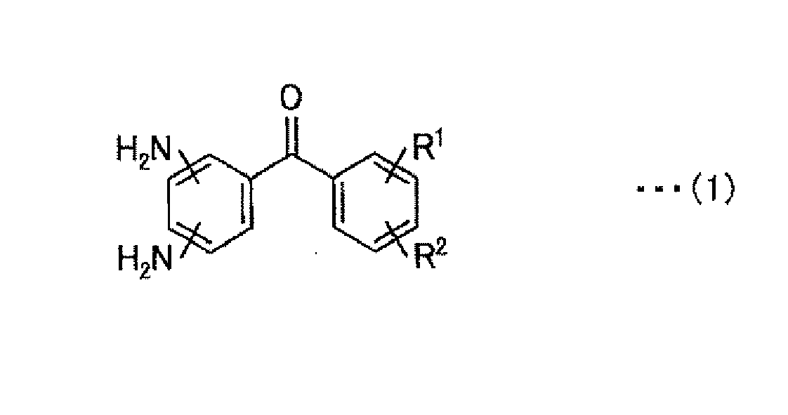
11―140186 - According to one aspect of the present invention, there is provided a laminate structure including a substrate, a wettability changing layer, and an electrical conductor layer, wherein the wettability changing layer and the electrical conductor layer are laminated on the substrate in order, wherein the wettability changing layer contains a polyimide, wherein the polyimide is obtainable by dehydrating and ring-opening a polyamic acid, wherein the polyamic acid is obtainable by ring-opening and addition-polymerizing a diamine and a tetracarboxylic acid dianhydride, wherein the diamine includes a compound represented by a general formula of:


- According to another aspect of the present invention, there is provided a method for manufacturing a laminate structure, including a step of forming a wettability changing layer containing a polyimide on a substrate, a step of irradiating a predetermined area of the wettability changing layer with an ultraviolet ray, and a step of forming an electrical conductor layer on an ultraviolet-ray-irradiated area of the wettability changing layer, wherein the polyimide is obtainable by dehydrating and ring-opening a polyamic acid, wherein the polyamic acid is obtainable by ring-opening and addition-polymerizing a dimaine and a tetracarboxylic acid dianhydride, wherein the diamine includes a compound represented by a general formula of:


- According to another aspect of the present invention, there is provided an electronic element array including the laminate structure as described above.
- According to another aspect of the present invention, there is provided an image displaying medium including the electronic element array as described above.
- According to another aspect of the present invention, there is provided an image displaying apparatus including the image displaying medium as described above.
- According to another aspect of the present invention, there is provided a diamine being a compound represented by a general formula of:

- According to another aspect of the present invention, there is provided a polyamic acid being obtainable by ring-opening and addition-polymerizing a diamine including the diamine as described above and a tetracarboxylic acid dianhydride.
- According to another aspect of the present invention, there is provided a polyimide being obtainable by dehydrating and ring-opening the polyamic acid as described above.
-
-
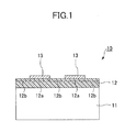
FIG. 1 is a cross-sectional view illustrating one example of a laminate structure according to an embodiment of the present invention. -
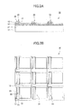
FIG. 2A and 2B are a diagram illustrating one example of an electronic element array according to an embodiment of the present invention. -
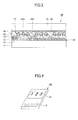
FIG. 3 is a cross-sectional view illustrating one example of an image displaying medium according to an embodiment of the present invention. -
FIG. 4 is a perspective view illustrating one example of an image displaying apparatus according to an embodiment of the present invention. -
FIG. 5 is a 1H NMR spectrum of diamine (1). -
FIG. 6 is an IR spectrum of diamine (1). -
FIG. 7 is a 1H NMR spectrum of polyimide (1). -
FIG. 8 is a DSC thermogram of polyimide (1). -
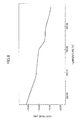
FIG. 9 is a diagram illustrating results of evaluation of contact angles for practical example 3 and comparative example 3. - Next, an embodiment(s) for implementing the present invention will be described in conjunction with the drawings.
- At least one embodiment of the present invention relates to at least one of a laminate structure, a method for manufacturing a laminate structure, an electronic element array, an image displaying medium, an image displaying apparatus, a diamine, a polyamic acid, and a polyimide.
- While a problem(s) possessed by the above-mentioned conventional technique(s) may be taken into consideration, an embodiment of the present invention may aim at providing at least one of a laminate structure in which a change in its surface free energy due to irradiation with an ultraviolet ray(s) may be large, and an electronic element array, image displaying medium, and image displaying apparatus including the laminate structure.
- Also, an embodiment of the present invention may aim at providing at least one of a polyimide in which a change in its surface free energy due to irradiation with an ultraviolet ray(s) may be large, a polyamic acid which may be a precursor of the polyimide, and a diamine which may be a structural unit of the polyimide.
- In a laminate structure according to an embodiment of the present invention, a wettability changing layer which contains a polyimide, and an electrical conductor layer are laminated on a substrate in order, wherein the polyimide is obtainable by dehydrating and ring-opening a polyamic acid, wherein the polyamic acid is obtainable by ring-opening and addition-polymerizing a diamine and a tetracarboxylic acid dianhydride, wherein the diamine includes a compound represented by a general formula of:


- A method for manufacturing a laminate structure according to an embodiment of the present invention includes a step of forming a wettability changing layer which contains a polyimide on a substrate, a step of irradiating a predetermined area of the wettability changing layer with a ultraviolet ray(s), and a step of forming an electrical conductor layer on an ultraviolet ray irradiated area of the wettability changing layer, wherein the polyimide is obtainable by dehydrating and ring-opening a polyamic acid, wherein the polyamic acid is obtainable by ring-opening and addition-polymerizing a diamine and a tetracarboxylic acid dianhydride, wherein the diamine includes a compound represented by a general formula of:


- An electronic element array according to an embodiment of the present invention includes the laminate structure according to an embodiment of the present invention.
- An image displaying medium according to an embodiment of the present invention includes the electronic element array according to an embodiment of the present invention.
- An image displaying apparatus according to an embodiment of the present invention includes the image displaying medium according to an embodiment of the present invention.
- A diamine according to an embodiment of the present invention is a compound represented by a general formula of:

- A polyamic acid according to an embodiment of the present invention is obtainable by ring-opening and addition-polymerizing a diamine which includes the diamine according to an embodiment of the present invention, and a tetracarboxylic acid dianhydride.
- A polyimide according to an embodiment of the present invention is obtainable by dehydrating and ring-opening the polyamic acid according to an embodiment of the present invention.
- According to at least one embodiment of the present invention, it may be possible to provide at least one of a laminate structure in which a change in its surface free energy due to irradiation with an ultraviolet ray(s) may be large, and an electronic element array, image displaying medium, and image displaying apparatus including the laminate structure.
- Also, according to at least one embodiment of the present invention, it may be possible to provide at least one of a polyimde in which a change in its surface free energy due to irradiation with an ultraviolet ray(s) may be large, a polyamic acid which may be a precursor of the polyimide, and a diamine which may be a structural unit of the polyimide.
-
FIG. 1 illustrates one example of a laminate structure according to an embodiment of the present invention. For alaminate structure 10, awettability changing layer 12 containing a polyimide according to an embodiment of the present invention is formed on asubstrate 11. Herein, thewettability changing layer 12 is composed of ultraviolet ray irradiatedareas 12a whose surface free energy has been increased by irradiation with ultraviolet rays and ultraviolet ray non-irradiatedareas 12b which have not been irradiated with ultraviolet rays. Additionally, the ultraviolet raynon-irradiated area 12b with a width of 1 - 5 µm is formed between the ultraviolet ray irradiatedareas 12a. Furthermore,electrical conductor layers 13 are formed on the ultraviolet ray irradiatedareas 12a of thewettability changing layer 12, so as to provide a laminate structure. Thereby, it may be possible to readily form theelectrical conductor layers 13 having a fine pattern. - A material constituting the
substrate 11 is not particularly limited and there may be provided a glass; a resin such as a polyester, a polycarbonate, a polyacrylate, a polyether sulfone, a polyethylene terephthalate, or a polyethylene naphthalate; a metal such as SUS; or the like, wherein a resin may be preferable if flexibility is required. - A polyimide according to an embodiment of the present invention includes one which is obtainable by dehydrating and ring-opening a polyamic acid according to an embodiment of the present invention while using a publicly-known method and has a remaining part of amide linkages thereof. Furthermore, a polyamic acid according to an embodiment of the present invention is obtainable by ring-opening and addition-polymerizing a diamine including a diamine according to an embodiment of the present invention and a tetracarboxylic acid dianhydride while using a publicly-known method.
- A diamine according to an embodiment of the present invention is a compound represented by general formula (1).
- Herein, each of an alkyl group and an alkoxy group for any of R1 and R2 may be linear or may be branched. Furthermore, each of an alkyl group and an alkoxy group for any of R1 and R2 may include a cycloalkyl group or a cycloalkylene group.
- If a carbon number of at least one of an alkyl group and an alkoxy group for any of R1 and R2 is 1 - 5, a change in the surface free energy of the
wettability changing layer 12 due to irradiation with ultraviolet rays may be insufficient, and if it is 21 or more, a solubility of a polyimide according to an embodiment of the present invention in an aprotic and polar organic solvent may be insufficient. - A method for synthesizing a diamine according to an embodiment of the present invention will be described below.
- A method for synthesizing diamine (1) represented by a chemical formula of:

- First, 1,4-didodecylbenzene represented by a chemical formula of:


- . Then, dinitro body (1) is subjected to catalytic reduction to obtain diamine (1).
- Next, a method for synthesizing diamine (2) represented by a chemical formula of:

- First, a dipotassium salt of hydroquinone represented by a chemical formula of:


- Then, ether body (1) and 3,5-dinitrobenzoyl chloride are subjected to electrophilic substitution to obtain a dinitro body (2) represented by a chemical formula of:

- Furthermore, dinitro body (2) is subjected to catalytic reduction to obtain diamine (2).
- Preferably, a diamine to be used for synthesizing a polyamic acid according to an embodiment of the present invention may further contain an aromatic and cyclic diamine other than a diamine according to an embodiment of the present invention.
- The aromatic and cyclic diamine is not particularly limited and there may be provided p-phenylenediamine, 4,4-methylenediamine, 4,4'-oxydianiline, m-bis(aminophenoxy)diphenyl sulfone, p-bis(aminophenoxy)diphenyl sulfone, 2,2-bis[(aminophenoxy)phenyl]propane, 2,2-bis[(aminophenoxy)phenyl]hexafluoropropane, or the like, wherein two or more kinds thereof may be used in combination.
- Furthermore, the diamine may further include a diaminosiloxane represented by a general formula of:

- A molar ratio of a diamine according to an embodiment of the present invention based on a total amount of the diamine may be usually 0.1 - 0.7 and preferably 0.2 ― 0.5. If a molar ratio of a diamine according to an embodiment of the present invention based on a total amount of the diamine is less than 0.1, a change of a surface free energy of the
wettability changing layer 12 due to irradiation with an ultraviolet ray(s) may be insufficient, and if it is greater than 0.7, a solubility of a polyimide according to an embodiment of the present invention in an aprotic and polar organic solvent may be insufficient. - Preferably, a tetracarboxylic acid dianhydride to be used for synthesizing a polyamic acid according to an embodiment of the present invention may include an alicyclic tetracarboxylic acid dianhydride.
- The alicyclic tetracarboxylic acid dianhydride is not particularly limited and there may be provided 5-(2,5-dioxotetrahydrofuryl)-3-methylcyclohexene-1,2-dicarboxylic acid dianhydride, bicyclooctene-2,3,5,6-tetracarboxylic acid dianhydride, 1,2,3,4-cyclobutanetetracarboxylic acid dianhydride, 1,2,3,4-cyclopentanetetracarboxylic acid dianhydride, 1,2,4,5-cyclohexanetetracarboxylic acid dianhydride, or the like, wherein two or more kinds thereof may be used in combination.
- Furthermore, the tetracarboxylic acid dianhydride may include an aromatic and cyclic tetracarboxylic acid dianhydride in place of the alicyclic tetracarboxylic acid dianhydride or in combination with the alicyclic tetracarboxylic acid dianhydride.
- The aromatic and cyclic tetracarboxylic acid dianhydride is not particularly limited and there may be provided pyromellitic acid dianhydride, biphthalic acid dianhydride, oxydiphthalic acid dianhydride, benzophenonetetracarboxylic acid dianhydride, hexafluoroisopropylidenediphthalic acid dianhydride, or the like, wherein two or more kinds thereof may be used in combination.
- A molar ratio of an alicyclic tetracarboxylic acid dianhydride based on a total amount of the tetracarboxylic acid dianhydride may be usually 0.2 - 1.0 and preferably 0.5 - 1. If a molar ratio of an alicyclic tetracarboxylic acid dianhydride based on a total amount of the tetracarboxylic acid dianhydride is less than 0.2, an insulating property of the
wettability changing layer 12 may be degraded due to irradiation with an ultraviolet ray(s). - Preferably, a number-average molecular weight of a polyamic acid according to an embodiment of the present invention may be 5 × 10³ - 5 × 10⁵. Accordingly, it may be possible for a glass transition point of a polyimide according to an embodiment of the present invention to be 200 - 350 °C.
- Herein, the number-average molecular weight is a molecular weight in terms of polystyrene which is measured by using a GPC (gel permeation chromatography).
- It may be possible to form the
wettability changing layer 12 by applying to thesubstrate 11 an application fluid in which a polyamic acid according to an embodiment of the present invention is dissolved in an aprotic and polar organic solvent and subsequently dehydrating and ring-opening such a polyamic acid according to an embodiment of the present invention. - The aprotic and polar organic solvent is not particularly limited and there may be provided N-methyl-2-pyrolidone, γ-butyrolactone, dimethylformamide, dimethylacetamide, tetrahydrofuran, or the like.
- A method for applying an application fluid to the
substrate 11 is not particularly limited and there may be provided a dip coat method, a spin coat method, a transfer printing method, a roll coat method, an ink jet method, a spray method, a brush coating method, or the like. - A rate of reaction of dehydrating and ring-opening of a polyamic acid according to an embodiment of the present invention may be preferably 90 - 100% and more preferably 95 - 100%. If the rate of reaction is less than 90%, it may not be possible to form a good interface between the
wettability changing layer 12 and an organic semiconductor layer when thewettability changing layer 12 is used as a gate insulating film of an organic thin-film transistor. Accordingly, a variation of a threshold voltage of such an organic thin-film transistor may increase. - Herein, it may be possible to measure the rate of reaction by dissolving a polyimide in dimethylsulfoxide (DMSO) - d6 to measure 1HNMR thereof and calculating a ratio of a remaining amide linkage(s) from a ratio of peak surface areas therein.
- Preferably, a polyimide according to an embodiment of the present invention may be soluble in an aprotic and polar organic solvent. In such a case, it may be possible to form the
wettability changing layer 12 by applying to thesubstrate 11 an application fluid in which a polyimide according to an embodiment of the present invention is dissolved in an aprotic and polar solvent. Herein, the application fluid may further contain a polyamic acid according to an embodiment of the present invention. - The
wettability changing layer 12 includes a polyimide according to an embodiment of the present invention which has an alkyl group or an alkoxy group in a side chain thereof so as to be hydrophobic and have a smaller surface free energy. - Meanwhile, when the
wettability changing layer 12 is irradiated with an ultraviolet ray(s), it is considered that a polyimide according to an embodiment of the present invention may be photo-dissociated so as to be hydrophilic, that is, to have a larger surface free energy. When a polyimide according to an embodiment of the present invention is photo-dissociated, a radical may be generated and a generated radical may immediately react with moisture contained in atmosphere so as to produce a carboxylic group or a hydroxyl group. - Additionally, the
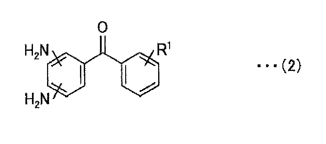
wettability changing layer 12 may contain a polyimide identical to a polyimide according to an embodiment of the present invention in place of the polyimide according to an embodiment of the present invention or in combination with the polyimide according to an embodiment of the present invention except that a compound represented by general formula (2) is used in place of a diamine according to an embodiment of the present invention. - Herein, an alkyl group and alkoxy group for R1 in a compound represented by general formula (2) are similar to an alkyl group and alkoxy group for R1 in a compound represented by general formula (1), respectively.
- Furthermore, the
wettability changing layer 12 may further contain an insulating resin. - The insulating resin is not particularly limited and there may be provided a polyimide, a polyamideimide, an epoxy resin, a silsesquioxane, a polyvinylphenol, a polycarbonate, a fluororesin, a poly(p-xylylene), or the like.
- Furthermore, the
wettability changing layer 12 may further contain a film-forming resin. - A thickness of the
wettability changing layer 12 may be usually 30 nm - 3 µm and preferably 50 nm - 1 µm. If a thickness of thewettability changing layer 12 is less than 30 nm, uniform formation thereof may be difficult, and if it is greater than 3 µm, a surface shape thereof may be degraded. - It may be possible to form the
electrical conductor layer 13 by applying, and subsequently heating or irradiating with an ultraviolet ray(s), an application fluid containing an electrically conductive material. - The electrically conductive material is not particularly limited and there may be provided a metal such as gold, silver, copper, aluminum, or calcium; a carbon material such as a carbon black, a fullerene, or a carbon nanotube; an organic π-conjugate polymer such as a polythiophene, a polyaniline, a polypyrrole, a polyfluorene, or a derivative thereof; or the like, wherein two or more kinds thereof may be used in combination. Additionally, when a gate electrode and source and drain electrodes are formed, electrically conductive materials different from one another may be used.
- The application fluid containing an electrically conductive material is not particularly limited and there may be provided a solution in which an electrically conductive material or a precursor thereof is dissolved in a solvent, a dispersion fluid in which an electrically conductive material or a precursor thereof is dispersed in a solvent, or the like.
- The solvent is not particularly limited, and there may be provided water, each kind of alcohol, or the like because damage to the
wettability changing layer 12 may be small. Furthermore, it may also be possible to use a solvent such as N,N-dimethylformamide, N,N-dimethylacetamide, 2-pyrolidone, N-methyl-2-pyrolidone, N-ethyl-2-pyrolidone, N-vinyl-2-pyrolidone, N-methylcaprolactam, dimethyl sulfoxide, or tetramethylurea, as long as damage to thewettability changing layer 12 may be small. - For the application fluid containing an electrically conductive material, there may be provided a dispersion fluid in which a particle(s) of a metal such as silver, gold, nickel, or copper is/are dispersed in an organic solvent or water, an aqueous solution of a doped PANI (polyaniline), an aqueous solution of an electrically conductive polymer in which a PEDOT (polyethylenedioxythiophene) is doped with a PSS (polystyrenesulfonic acid), or the like.
- A method for applying the application fluid containing an electrically conductive material is not particularly limited and there may be provided a spin coat method, a dip coat method, a screen printing method, an offset printing method, an ink jet method, or the like. Among these, an ink jet method may be preferable because of susceptibleness to influence of a surface free energy of the
wettability changing layer 12. - Although the resolution and landing precision of a normal ink jet head at a level to be used in an ink jet printer are about 30 µm and about ± 15 µm, respectively, it may be possible to form the
electrical conductor layer 13 having a fine pattern by utilizing a difference between surface free energies of thewettability changing layer 12. - It may be possible to apply a laminate structure according to an embodiment of the present invention to a gate electrode and its wiring of an organic thin-film transistor, source and drain electrodes and their wiring thereof, or the like.
-
FIGS. 2A and 2B illustrate a thin-film transistor array as one example of an electronic element array according to an embodiment of the present invention. A thin-film transistor array 30 has a plurality of bottom-gate-type thin-film transistors 20. Herein,FIG. 2A and 2B are a cross-sectional view and top view thereof, respectively. Furthermore, an identical reference numeral is provided for an element inFIG. 2A and 2B which is identical to that ofFIG. 1 and an explanation thereof will be omitted. - For the thin-
film transistor 20,gate electrodes 21 are formed on asubstrate 11. Furthermore,wettability changing layers 12 as gate insulating films are formed on thesubstrate 11 on which thegate electrodes 21 are formed, and electrical conductor layers 13 as source and drain electrodes are formed on ultraviolet-ray-irradiated areas of the wettability changing layers 12. Moreover, semiconductor layers 22 are formed on channel areas between the source and drain electrodes. Thus, it may be possible to readily form gate electrodes and source and drain electrodes having a fine pattern. - The
semiconductor layer 22 may be any of an inorganic semiconductor layer and an organic semiconductor layer, wherein an organic semiconductor layer may be preferable because it may be possible to simplify, or reduce the cost of, a process for manufacturing a thin-film transistor. - A material for composing the inorganic semiconductor layer is not particularly limited and there may be provided CdSe, CdTe, Si, or the like.
- A method for forming the inorganic semiconductor layer is not particularly limited and there may be provided a method using a vacuum process such as sputtering, a sol-gel method, or the like.
- A material for composing the organic semiconductor layer is not particularly limited and there may be provided a low molecule such as pentacene, anthracene, tetracene, or phthalocyanine; a polyacetylene-type electrically conductive polymer; a polyphenylene-type electrically conductive polymer such as a poly(p-phenylene) or a derivative thereof or a polyphenylenevinylene or a derivative thereof; a heterocyclic electrically coinductive polymer such as a polypyrrole or a derivative thereof, a polythiophene or a derivative thereof, or a polyfuran or a derivative thereof; an ionic electrically conductive polymer such as a polyaniline or a derivative thereof; or the like.
- A method for forming the orranic semiconductor layer is not particularly limited and there may be provided a spin coat method, a spray coat method, a printing method, an ink jet method, or the like.
- Additionally,
wettability changing layers 12 may be formed asubstrate 11 in place of forming of thegate electrodes 21, and electrical conductor layers 13 as gate electrodes may be formed on ultraviolet-ray-irradiated areas of the wettability changing layers 12. - Herein, polyimides according to an embodiment of the present invention which are contained in two of the
wettability changing layers 12 may be identical to or may be different from each other. Furthermore, electrically conductive materials which are contained in two of the electrical conductor layers 13 may be identical to or may be difficult from each other. - Meanwhile, when volume resistivities of the
wettability changing layers 12 are small, insulator layers with volume resistivities greater than those of thewettability changing layers 12 and thewettability changing layers 12 may be laminated in order so as to form gate insulating films. When such gate insulating films are irradiated with ultraviolet rays, it may be possible to suppress degradation of insulating properties of the insulator layers because thewettability changing layers 12 may absorb ultraviolet rays. - A material for composing the insulator layer is not particularly limited and there may be provided a polyimide, a polyamideimide, an epoxy resin, a silsesquioxane, a polyvinylphenol, a polycarbonate, a fluororesin, a poly(p-xylylene), or the like.
- A method for forming the insulator layer is not particularly limited and there may be provided a transfer printing method, a spin coat method, a dip coat method, or the like.
-
FIG. 3 illustrates an electrophoretic panel as one example of an image displaying medium according to an embodiment of the present invention. For anelectrophoretic panel 40, atransparent electrode 42 is formed on atransparent substrate 41, and animage displaying layer 43 composed ofmicrocapsules 43a as electrophoretic elements and abinder 43b is formed on theelectrode 42. Herein, themicrocapsule 43a encapsulates, for example, white titanium oxide particles and Isopar L (produced by Exxon Mobil Chemical) colored with oil blue. Furthermore, theimage displaying layer 43 is connected to a thin-film transistor array 30 as an active matrix substrate. - Additionally, an image displaying medium according to an embodiment of the present invention is not limited to an electrophoretic panel but may be a liquid crystal panel or organic EL panel in which an active matrix substrate is combined with an image displaying element such as a liquid crystal element or organic EL element, or the like. Furthermore, it may be possible to use an image displaying medium according to an embodiment of the present invention as an electronic paper.
- Herein, it may also be possible to apply a polyimide according to an embodiment of the present invention to a liquid crystal alignment film in a liquid crystal element or a bank in an organic EL element, other than a laminate structure.
-
FIG. 4 illustrates a pocket PC as one example of an image displaying apparatus according to an embodiment of the present invention. A pocket PC has anelectrophoretic panel 40 as a flat screen on which an image is displayed by inputting image information frominput parts 51. - Additionally, it may be possible to apply an electronic element array according to an embodiment of the present invention to a solar cell, an RFID tag, or the like, other than an image displaying medium.
- Furthermore, it may be possible to apply an image displaying medium according to an embodiment of the present invention to a copying machine or the like, other than an image displaying apparatus, and it may also be possible to be embedded in a seat part or front glass surface of a moving or transportation medium such as an automobile or an airplane, or the like.
- After 1 g of 1,4-didodecylbenzene, 0.61 g of 3,5-dinitrobenzoyl chloride, and nitromethane were charged into a two-necked flask and cooled to 10 °C or lower in an ice-water bath, 1.6 g of aluminum chloride was dropped therein while stirring was conducted. Then, heating and refluxing were conducted at 100 °C for 24 hours, and subsequently cooling to room temperature was conducted. Furthermore, a small amount of dichloromethane was added thereto, so as to dissolve a precipitated product, and subsequently, an oil phase was washed and dried under vacuum so as to obtain dinitro body (1).
- After 3.48 g of dinitro body (1) was charged into a pressure bottle, ethanol and tetrahydrofuran were added thereto. Then, a small amount of palladium on carbon was added thereto, and subsequently, catalytic reduction was conducted by using a catalytic reduction apparatus for about 2 hours. Furthermore, the palladium on carbon was removed, and subsequently, drying under vacuum was conducted. An obtained product was purified on a column to obtain diamine (1).
-
FIGS. 5 and6 illustrate a 1H NMR spectrum and IR spectrum of diamine (1), respectively. - After 0.5 mol of diamine (1) and 0.5 mol of a diamine represented by a chemical formula of:


- . A number-average molecular weight of polyamic acid (1) was 5500.
- After N-methyl-2-pyrolidone was added to polyamic acid (1), pyridine and acetic anhydride were added thereto and dehydration and ring-opening were conducted at 120 °C under argon atmosphere for 4 hours. After an obtained reaction fluid was dropped into stirred methanol to provide a precipitate, filtration under reduced pressure and drying under vacuum were conducted so as to obtain polyimide (1) represented by a chemical formula of:

-
FIGS. 7 and8 illustrate a 1H NMR spectrum and DSC thermogram of polyimide (1), respectively. - After a 10% by mass solution of polyimide (1) in N-methyl-2-pyrolidone was applied onto a
substrate 11 made of an inorganic alkali glass by using a spin coat method, baking at 200 °C under an inert gas atmosphere was conducted by using an oven so as to form awettability changing layer 12 with a thickness of 100 nm. - After the
wettability changing layer 12 was irradiated with ultraviolet rays with a wavelength of 254 nm by using a high pressure mercury lamp, a contact angle of a dispersion fluid in which silver nanoparticles were dispersed in an aqueous dispersion medium (referred to as a silver nanoink, below) was measured by a liquid drop method. The results of the measurement are presented in Table 1. - After a 10% by mass solution of polyimide (1) in N-methyl-2-pyrolidone was applied onto a
substrate 11 made of an inorganic alkali glass by using a spin coat method, baking at 200 °C under an inert gas atmosphere was conducted by using an oven so as to form awettability changing layer 12 with a thickness of 100 nm. Then, thewettability changing layer 12 was irradiated with ultraviolet rays with a wavelength of 254 nm by using a high pressure mercury lamp through a photomask having line shapes with a spacing of 5 µm. Furthermore, after the silver nanoink was applied onto an ultraviolet-ray-irradiated area by using an ink jet method, baking at 200 °C under an inert gas atmosphere was conducted by using an oven so as to form anelectrical conductor layer 13 and obtain a laminate structure 10 (seeFIG. 1 ). - The
electrical conductor layer 13 was observed by using a metallurgical microscope so as to evaluate a patterning characteristic thereof. The results of the evaluation are presented in Table 1. Herein, judgment was conducted such that "A", "B", and "C" were provided for 90% or greater, 10% or greater and less than 90%, and less than 10% of theelectrical conductor layer 13 having line shapes with a spacing of 5 µm having been formed, respectively. - After 10 g of hydroquinone, 75.31 g of potassium carbonate, and N,N-dimethylformamide were charged into a three-necked flask and heated in an oil bath at 70 °C under argon atmosphere, 45 g of 1-bromododecane was dropped thereto while stirring was conducted, and stirring was conducted at 70 °C for 24 hours. Then, cooling to room temperature was conducted, and subsequently, a reaction fluid was thrown into deionized water so as to provide a precipitate. Furthermore, the precipitate was filtered, and subsequently, washing operations were repeated. Then, recrystallization was conducted with a mixed liquid of ethyl acetate and ethanol, and subsequently, drying under vacuum was conducted so as to obtain ether body (1).
- After 1 g of ether body (1), 0.61 g of 3,5-dinitrobenzoyl chloride, and carbon disulfide were charged into a two-necked flask and cooled to 10 °C or lower in an ice-water bath, 1.6 g of aluminum chloride was dropped thereto while stirring was conducted. Then, heating and refluxing were conducted at 40 °C for 24 hours, and subsequently, cooled to room temperature. Furthermore, after a reaction fluid was quenched with a mixed liquid of ice water and hydrochloric acid, an oil phase was washed with deionized water and an aqueous solution of sodium hydroxide by using a separating funnel and dried under vacuum so as to obtain dinitro body (2).
- Diamine (2) was obtained similarly to practical example 1 except that dinitro body (2) was used in place of dinitro body (1).
- Polyamic acid (2) represented by a chemical formula of:

- Polyimide (2) represented by a chemical formula of:

- A contact angle of a silver nanoink was measured similarly to practical example 1 except that a 10% by mass solution of polyimide (2) in γ-butyrolactone was used in place of a 10% by mass solution of polyimide (1) in N-methyl-2-pyrolidone. The results of the measurement are presented in Table 1.
- A patterning characteristic was evaluated similarly to practical example 1 except that a 10% by mass solution of polyimide (2) in γ-butyrolactone was used in place of a 10% by mass solution of polyimide (1) in N-methyl-2-pyrolidone. The results of the measurement are presented in Table 1.
- A polyamic acid was obtained similarly to practical example 1 except that a diamine represented by a chemical formula of:

- A polyimide was obtained similarly to practical example 1 except that the obtained polyamic acid was used in place of polyamic acid (1).
- A contact angle of a silver nanoink was measured similarly to practical example 1 except that a 10% by mass solution of the obtained polyimide in N-methyl-2-pyrolidone was used in place of a 10% by mass solution of polyimide (1) in N-methyl-2-pyrolidone. The results of the measurement are presented in Table 1.
- A patterning characteristic was evaluated similarly to practical example 1 except that a 10% by mass solution of the obtained polyimide in N-methyl-2-pyrolidone was used in place of a 10% by mass solution of polyimide (1) in N-methyl-2-pyrolidone. The results of the measurement are presented in Table 1.
- A polyamic acid was obtained similarly to practical example 1 except that a diamine represented by a chemical formula of:

- A polyimide was obtained similarly to practical example 1 except that the obtained polyamic acid was used in place of polyamic acid (1).
- A contact angle of a silver nanoink was measured similarly to practical example 1 except that a 10% by mass solution of the obtained polyimide in N-methyl-2-pyrolidone was used in place of a 10% by mass solution of polyimide (1) in N-methyl-2-pyrolidone. The results of the measurement are presented in Table 1.
- A patterning characteristic was evaluated similarly to practical example 1 except that a 10% by mass solution of the obtained polyimide in N-methyl-2-pyrolidone was used in place of a 10% by mass solution of polyimide (1) in N-methyl-2-pyrolidone. The results of the measurement are presented in Table 1.
Table 1 Amount of ultraviolet ray irradiation [J/cm2] 0 1 2 3 5 Practical example 1 Contact angle [°] 33 13 5 5 4 Patterning characteristic C B A A A Practical example 2 Contact angle [°] 32 12 5 5 4 Patterning characteristic C B A A A Comparative example 1 Contact angle [°] 26 21 17 15 6 Patterning characteristic C C C B A Comparative example 2 Contact angle [°] 35 29 24 14 9 Patterning characteristic C C C B B - It was found from Table 1 that when the
wettability changing layer 12 for practical example 1 was irradiated with 2 J/cm2 of ultraviolet rays with a wavelength of 254 nm, polyimide (1) was photo-dissociated and accordingly the contact angle of the silver nanoink decreased from 33° to 5°. - Also, it was found that when the
wettability changing layer 12 for practical example 2 was irradiated with 2 J/cm2 of ultraviolet rays with a wavelength of 254 nm, polyimide (2) was photo-dissociated and accordingly the contact angle of the silver nanoink decreased from 32° to 5°. - On the other hand, it was found that even when the wettability changing layer for comparative example 1 was irradiated with 5 J/cm2 of ultraviolet rays with a wavelength of 254 nm, the contact angle of the silver nanoink only decreased from 26° to 6°.
- Also, it was found that even when the wettability changing layer for comparative example 2 was irradiated with 5 J/cm2 of ultraviolet rays with a wavelength of 254 nm, the contact angle of the silver nanoink only decreased from 35° to 9°.
- As a result, it was found that a change of a surface free energy of the
wettability changing layer 12 for practical example 1 or 2 due to irradiation with ultraviolet rays with a wavelength of 254 nm was greater than that of the wettability changing layer for comparative example 1 or 2. - Also, it was found from Table 1 that the results of evaluation of the patterning characteristic correlated with the results of evaluation of a change of the contact angle.
- Polyamic acid (3) represented by a chemical formula of:


- Polyimide (3) represented by a chemical formula of:

- A contact angle of a silver nanoink was measured similarly to practical example 1 except that a 10% by mass solution of polyimide (3) in N-methyl-2-pyrolidone was used in place of a 10% by mass solution of polyimide (1) in N-methyl-2-pyrolidone. The results of the measurement are illustrated in
FIG. 9 . - A patterning characteristic was evaluated similarly to practical example 1 except that a 10% by mass solution of polyimide (3) in N-methyl-2-pyrolidone was used in place of a 10% by mass solution of polyimide (1) in N-methyl-2-pyrolidone. The results of the evaluation are presented in Table 2.
- A polyamic acid was obtained similarly to practical example 1 except that a diamine represented by a chemical formula of:

- A polyimide was obtained similarly to practical example 1 except that the obtained polyamic acid was used in place of polyamic acid (1).
- A contact angle of a silver nanoink was measured similarly to practical example 1 except that a 10% by mass solution of the obtained polyimide in N-methyl-2-pyrolidone was used in place of a 10% by mass solution of polyimide (1) in N-methyl-2-pyrolidone. The results of the measurement are illustrated in
FIG. 9 . - A patterning characteristic was evaluated similarly to practical example 1 except that a 10% by mass solution of the obtained polyimide in N-methyl-2-pyrolidone was used in place of a 10% by mass solution of polyimide (1) in N-methyl-2-pyrolidone. The results of the evaluation are presented in Table 2.
Table 2 Amount of ultraviolet ray irradiation [J/cm2] 0 1 2 5 9 Practical example 3 C A A ― ― Comparative example 3 C C C B A - It was found from
FIG. 9 that when thewettability changing layer 12 for practical example 3 was irradiated with 2 J/cm2 of ultraviolet rays with a wavelength of 254 nm, polyimide (3) was photo-dissociated and accordingly the contact angle of the silver nanoink decreased from 25° to 5°. - On the other hand, it was found that when the wettability changing layer for comparative example 3 was irradiated with 9 J/cm2 of ultraviolet rays with a wavelength of 254 nm, the contact angle of the silver nanoink decreased from 28° to 5°.
- As a result, it was found that a surface free energy of the
wettability changing layer 12 for practical example 3 was changed with an amount of ultraviolet ray irradiation lower than that for the wettability changing layer for comparative example 3. - Also, it was found from
FIG. 9 and Table 2 that the results of evaluation of the patterning characteristic correlated with the results of evaluation of a change of the contact angle. - After aluminum was deposited under vacuum by using a metal mask so that
gate electrodes 21 with a thickness of 50 nm were formed on asubstrate 11 made of a glass, gate insulating films having a thickness of 500 nm and being composed of parylene were formed on thesubstrate 11 on which thegate electrodes 21 had been formed. Then, a solution of polyimide (3) for practical example 3 in N-methyl-2-pyrolidone was applied onto thesubstrate 11 on which the gate insulating films had been formed, by using a spin coat method, and subsequently, baking at 200 °C under an inert gas atmosphere was conducted by using an oven so as to formwettability changing layers 12 with a thickness of 100 nm. Furthermore, thewettability changing layers 12 were irradiated with 1 J/cm2 of ultraviolet rays with a wavelength of 254 nm through a photomask by using a high pressure mercury lamp. Then, the silver nanoink was applied onto ultraviolet-ray-irradiated areas by using an ink jet method, and subsequently, baking at 200 °C under an inert gas atmosphere was conducted by using an oven so as to form electrical conductor layers 13 (source electrodes and drain electrodes with a channel length of 5 µm). Furthermore, a solution of a compound represented by a chemical formula of:
FIG. 2A and 2B ). The thin-film transistor array 1 has 32 × 32 thin-film transistors 20 with a spacing of 500 µm. - After a solution of polyimide (3) for practical example 3 in N-methyl-2-pyrolidone was applied onto a
substrate 11 made of an inorganic alkali glass by using a spin coat method, baking at 180 °C under an inert gas atmosphere was conducted by using an oven so as to form wettability changing layers with a thickness of 80 nm. Then, the wettability changing layers were irradiated with 1 J/cm2 of ultraviolet rays with a wavelength of 254 nm through a photomask by using a high pressure mercury lamp. Furthermore, the silver nanoink was applied onto ultraviolet-ray-irradiated areas by an ink jet method, and subsequently, baking at 180 °C under an inert gas atmosphere was conducted by using an oven so as to formgate electrodes 21. Then, a solution of polyimide (3) for practical example 3 and polyimide CT4112 (produced by KYOCERA Chemical Corporation) in N-methyl-2-pyrolidone was applied by using a spin coat method, and subsequently, baking at 180 °C under an inert gas atmosphere was conducted by using an oven so as to form wettability changing layers 12 (gate insulating films) with a thickness of 800 nm. Furthermore, thewettability changing layers 12 were irradiated with 1 J/cm2 of ultraviolet rays with a wavelength of 254 nm through a photomask by using a high pressure mercury lamp. Then, the silver nanoink was applied onto ultraviolet-ray-irradiated areas by using an ink jet method, and subsequently, baking at 150 °C under an inert gas atmosphere was conducted by using an oven so as to form electrical conductor layers 13 (source electrodes and drain electrodes with a channel length of 5 µm). Furthermore, semiconductor layers 22 with a thickness of 30 nm were formed on channel areas between the source electrodes and the drain electrodes similarly to thin-film transistor array 1, so as to obtain thin-film transistor array 2. Thin-film transistor array 2 has 32 × 32 thin-film transistors 20 with a spacing of 500 µm. - Thin-
film transistor 3 was obtained similarly to thin-film transistor array 1 except that the solution of the polyimide for comparative example 3 in N-methyl-2-pyrolidone was used in place of the solution of polyimide (3) for practical example 3 in N-methyl-2-pyrolidone and wettability changing layers were irradiated with 9 J/cm2 of ultraviolet rays with a wavelength of 254 nm. - The results of evaluation of transistor characteristics of the thin-film transistor arrays are presented in Table 3.
Table 3 Thin-film transistor array Polyimide Amount of ultraviolet ray irradiation [J/cm2] Electric-field-effect mobility [cm2/V·sec] On- off ratio 1 Practical example 3 1 5 × 10⁻³ 5 digits 2 Practical example 3 1 2 × 10⁻³ 5 digits 3 Comparative example 3 9 1 × 10⁻⁴ 3 digits - It was found from Table 3 that thin-
film transistor array - On the other hand, thin-
film transistor array 3 had a smaller electric-field-effect mobility as well as a larger gate leak electric current and a smaller on-off ratio. It was considered that this was because an amount of irradiation of the ultraviolet rays with a wavelength of 254 nm was greater. - An electrophretic panel (see
FIG. 3 ) was manufactured by using thin-film transistor array 2. Specifically, an application fluid in whichmicrocapsules 43a encapsulating titanium oxide particles and Isopar colored with oil blue and an aqueous solution of apolyvinyl alcohol 43b were mixed was applied onto transparent electrodes made ofITO 42 and formed on atransparent substrate 41 made of a polycarbonate so as to form animage displaying layer 43 composed ofmicrocapsules 43a and apolyvinyl alcohol 43b. Furthermore, theimage displaying layer 43 and the thin-film transistor array 30 were bonded such that thesubstrate 11 and thetransparent substrate 41 had outermost surfaces, thereby obtaining anelectrophoretic panel 40. - When a driver IC for scanning signals was connected to bus lines which were interconnected to
gate electrodes 21 of theelectrophoretic panel 40 while a driver IC for data signals was connected to bus lines which were interconnected to source electrodes and switching between images was conducted every 0.5 seconds, it was possible to display good static images. - Some illustrative embodiments (1) to (12) of the present invention will be described below.
- Embodiment (1) is a laminate structure characterized in that a wettability changing layer containing a polyimide and an electrical conductor layer are laminated on a substrate in order, wherein the polyimide is obtainable by dehydrating and ring-opening a polyamic acid, wherein the polyamic acid is obtainable by ring-opening and addition-polymerizing a diamine and a tetracarboxylic acid dianhydride, wherein the diamine includes a compound represented by a general formula of:


- Embodiment (2) is the laminate structure as recited in embodiment (1), characterized in that the diamine further includes an aromatic and cyclic diamine.
- Embodiment (3) is the laminate structure as recited in embodiment (1) or (2), characterized in that the tetracarboxylic acid dianhydride includes an alicyclic tetracarboxylic acid dianhydride.
- Embodiment (4) is the laminate structure as recited in any one of embodiments (1) to (3), characterized in that a number-average molecular weight of the polyamic acid is 5 × 10³ or greater and 5 × 10⁵ or less.
- Embodiment (5) is a method for manufacturing a laminate structure, characterized by including a step of forming a wettability changing layer containing a polyimide on a substrate, a step of irradiating a predetermined area of the wettability changing layer with an ultraviolet ray, and a step of forming an electrical conductor layer on an ultraviolet-ray-irradiated area of the wettability changing layer, wherein the polyimide is obtainable by dehydrating and ring-opening a polyamic acid, wherein the polyamic acid is obtainable by ring-opening and addition-polymerizing a dimaine and a tetracarboxylic acid dianhydride, wherein the diamine includes a compound represented by a general formula of:


- Embodiment (6) is the method for manufacturing a laminate structure as recited in embodiment (5), characterized in that an application fluid containing the polyimide and/or polyamic acid having a solubility is applied onto the substrate to form the wettability changing layer.
- Embodiment (7): An electronic element array characterized by including the laminate structure as recited in any one of embodiments (1) to (4).
- Embodiment (8) is an image displaying medium characterized by including the electronic element array as recited in embodiment (7).
- Embodiment (9) is an image displaying apparatus characterized by including the image displaying medium as recited in embodiment (8).
- Embodiment (10) is a diamine characterized by being a compound represented by a general formula of:

- Embodiment (11) is a polyamic acid characterized by being obtainable by ring-opening and addition-polymerizing a diamine including the diamine recited in embodiment (10) and a tetracarboxylic acid dianhydride.
- Embodiment (12) is a polyimide characterized by being obtainable by dehydrating and ring-opening the polyamic acid as recited in embodiment (11).
- Although the illustrative embodiment(s) and specific example(s) of the present invention have been described with reference to the accompanying drawing(s), the present invention is not limited to any of the illustrative embodiment(s) and specific example(s), and the illustrative embodiment(s) and specific example(s) may be altered, modified, or combined without departing from the scope of the present invention.
- The present application claims the benefit of its priority based on Japanese patent application No.
2011-129010 filed on June 9, 2011
Claims (12)
- A laminate structure characterized by comprising:a substrate;a wettability changing layer; andan electrical conductor layer;wherein the wettability changing layer and the electrical conductor layer are laminated on the substrate in order;wherein the wettability changing layer contains a polyimide;wherein the polyimide is obtainable by dehydrating and ring-opening a polyamic acid;wherein the polyamic acid is obtainable by ring-opening and addition-polymerizing a diamine and a tetracarboxylic acid dianhydride;wherein the diamine includes a compound represented by a general formula of:

 wherein each of R1 and R2 in formula (1) is independently an alkyl group with a carbon number of 6 or more and 20 or less or an alkoxy group with a carbon number of 6 or more and 20 or less; andwherein R1 in formula (2) is an alkyl group with a carbon number of 6 or more and 20 or less or an alkoxy group with a carbon number of 6 or more and 20 or less.
 - The laminate structure according to claim 1, wherein the diamine further includes an aromatic and cyclic diamine.
- The laminate structure according to claim 1 or 2, wherein the tetracarboxylic acid dianhydride includes an alicyclic tetracarboxylic acid dianhydride.
- The laminate structure according to any one of claims 1 to 3, wherein a number-average molecular weight of the polyamic acid is 5 × 10³ or greater and 5 × 10⁵ or less.
- A method for manufacturing a laminate structure, characterized by comprising:a step of forming a wettability changing layer containing a polyimide on a substrate;a step of irradiating a predetermined area of the wettability changing layer with an ultraviolet ray; anda step of forming an electrical conductor layer on an ultraviolet-ray-irradiated area of the wettability changing layer;wherein the polyimide is obtainable by dehydrating and ring-opening a polyamic acid;wherein the polyamic acid is obtainable by ring-opening and addition-polymerizing a dimaine and a tetracarboxylic acid dianhydride;wherein the diamine includes a compound represented by a general formula of:

 wherein each of R1 and R2 in formula (1) is independently an alkyl group with a carbon number of 6 or more and 20 or less or an alkoxy group with a carbon number of 6 or more and 20 or less; andwherein R1 in formula (2) is an alkyl group with a carbon number of 6 or more and 20 or less or an alkoxy group with a carbon number of 6 or more and 20 or less.
 - The method for manufacturing a laminate structure according to claim 5, wherein an application fluid containing the polyimide and/or polyamic acid having a solubility is applied onto the substrate to form the wettability changing layer.
- An electronic element array characterized by comprising the laminate structure according to any one of claims 1 to 4.
- An image displaying medium characterized by comprising the electronic element array according to claim 7.
- An image displaying apparatus characterized by comprising the image displaying medium according to claim 8.
- A diamine characterized by being a compound represented by a general formula of:

- A polyamic acid characterized by being obtainable by ring-opening and addition-polymerizing a diamine including the diamine according to claim 10 and a tetracarboxylic acid dianhydride.
- A polyimide characterized by being obtainable by dehydrating and ring-opening the polyamic acid according to claim 11.
Applications Claiming Priority (1)
| Application Number | Priority Date | Filing Date | Title |
|---|---|---|---|
| JP2011129010A JP5899668B2 (en) | 2011-06-09 | 2011-06-09 | Laminated structure and manufacturing method thereof |
Publications (2)
| Publication Number | Publication Date |
|---|---|
| EP2533317A2 true EP2533317A2 (en) | 2012-12-12 |
| EP2533317A3 EP2533317A3 (en) | 2015-09-09 |
Family
ID=46208350
Family Applications (1)
| Application Number | Title | Priority Date | Filing Date |
|---|---|---|---|
| EP12170848.1A Withdrawn EP2533317A3 (en) | 2011-06-09 | 2012-06-05 | Laminate structure, method for manufacturing a laminate structure, electronic element array, image displaying medium, image displaying apparatus, diamine, polyamic acid, and polyimide |
Country Status (3)
| Country | Link |
|---|---|
| US (1) | US20120315498A1 (en) |
| EP (1) | EP2533317A3 (en) |
| JP (1) | JP5899668B2 (en) |
Families Citing this family (3)
| Publication number | Priority date | Publication date | Assignee | Title |
|---|---|---|---|---|
| JP6197418B2 (en) | 2013-07-05 | 2017-09-20 | 株式会社リコー | Method for forming multilayer wiring, multilayer wiring, and electronic device |
| JP6248506B2 (en) * | 2013-09-25 | 2017-12-20 | Jnc株式会社 | Composition for forming cured film |
| JP2019001859A (en) * | 2017-06-13 | 2019-01-10 | Dic株式会社 | Polymer film surface modification method |
Citations (3)
| Publication number | Priority date | Publication date | Assignee | Title |
|---|---|---|---|---|
| JPH11140186A (en) | 1997-11-06 | 1999-05-25 | Kurume Tosu Chiiki Gijutsu Shinko Center | Photoreactive solvent soluble polyimide |
| JP2008041951A (en) | 2006-08-07 | 2008-02-21 | Ricoh Co Ltd | LAMINATED STRUCTURE, ELECTRONIC DEVICE USING LAMINATED STRUCTURE, METHOD FOR MANUFACTURING THE SAME, ELECTRONIC DEVICE ARRAY, AND DISPLAY DEVICE |
| JP2011129010A (en) | 2009-12-21 | 2011-06-30 | Denso It Laboratory Inc | Driving scene determination device, driving scene determination method and program, workload estimation device, and workload estimation method and program |
Family Cites Families (5)
| Publication number | Priority date | Publication date | Assignee | Title |
|---|---|---|---|---|
| CN101199041B (en) * | 2005-06-20 | 2010-05-19 | 日产化学工业株式会社 | Electrode pattern forming layer, method of manufacturing the same, pattern electrode, electronic device, and organic FET |
| JP5121264B2 (en) * | 2007-03-14 | 2013-01-16 | 株式会社リコー | Laminated structure and manufacturing method thereof |
| JP5211729B2 (en) * | 2008-02-07 | 2013-06-12 | 株式会社リコー | Laminated structure and manufacturing method thereof |
| JP5446751B2 (en) * | 2009-03-18 | 2014-03-19 | 株式会社リコー | Multilayer structure, electronic element, electronic element array, image display medium, and image display apparatus |
| JP5397017B2 (en) * | 2009-05-25 | 2014-01-22 | 株式会社リコー | Polyamide acid and polyimide |
-
2011
- 2011-06-09 JP JP2011129010A patent/JP5899668B2/en not_active Expired - Fee Related
-
2012
- 2012-06-05 EP EP12170848.1A patent/EP2533317A3/en not_active Withdrawn
- 2012-06-06 US US13/489,911 patent/US20120315498A1/en not_active Abandoned
Patent Citations (3)
| Publication number | Priority date | Publication date | Assignee | Title |
|---|---|---|---|---|
| JPH11140186A (en) | 1997-11-06 | 1999-05-25 | Kurume Tosu Chiiki Gijutsu Shinko Center | Photoreactive solvent soluble polyimide |
| JP2008041951A (en) | 2006-08-07 | 2008-02-21 | Ricoh Co Ltd | LAMINATED STRUCTURE, ELECTRONIC DEVICE USING LAMINATED STRUCTURE, METHOD FOR MANUFACTURING THE SAME, ELECTRONIC DEVICE ARRAY, AND DISPLAY DEVICE |
| JP2011129010A (en) | 2009-12-21 | 2011-06-30 | Denso It Laboratory Inc | Driving scene determination device, driving scene determination method and program, workload estimation device, and workload estimation method and program |
Also Published As
| Publication number | Publication date |
|---|---|
| JP2012254568A (en) | 2012-12-27 |
| US20120315498A1 (en) | 2012-12-13 |
| EP2533317A3 (en) | 2015-09-09 |
| JP5899668B2 (en) | 2016-04-06 |
Similar Documents
| Publication | Publication Date | Title |
|---|---|---|
| EP2240958B1 (en) | Laminated structure, method of manufacturing a laminated structure, electronic element, electronic element array, image displaying medium, and image displaying device | |
| EP2122672B1 (en) | Laminate structure and its manufacturing method | |
| JP2010199276A (en) | Thermoelectric conversion element and manufacturing method of same | |
| EP2162484B1 (en) | Polyamic acid | |
| JP5397017B2 (en) | Polyamide acid and polyimide | |
| US20120315498A1 (en) | Laminate structure, method for manufactuing laminate structure, electronic element array, image displaying medium, image displaying apparatus, diamine, polyamic acid, and polyimide | |
| US20150364688A1 (en) | Precursor dielectric composition with thiosulfate-containing polymers | |
| JP5446751B2 (en) | Multilayer structure, electronic element, electronic element array, image display medium, and image display apparatus | |
| US9691997B2 (en) | Devices having dielectric layers with thiosulfate-containing polymers | |
| JP5470788B2 (en) | ORGANIC SEMICONDUCTOR DEVICE, ORGANIC SEMICONDUCTOR DEVICE MANUFACTURING METHOD, ELECTRONIC DEVICE, AND ELECTRONIC DEVICE | |
| WO2010032834A1 (en) | Organic semiconductor device, method for manufacturing organic semiconductor device, electronic device, electronic apparatus and composition for forming insulating layer | |
| JP5761841B2 (en) | Organic semiconductor device having insulating layer containing phenolic hydroxyl group-containing aromatic polyamide resin and method for producing the same | |
| KR101187609B1 (en) | Low temperature processable and photo-crosslinkable organic gate insulator, and organic thin film transistor device using the same | |
| JP5412765B2 (en) | LAMINATED STRUCTURE, MULTILAYER WIRING BOARD, ACTIVE MATRIX SUBSTRATE, IMAGE DISPLAY DEVICE, AND LAMINATED STRUCTURE MANUFACTURING METHOD | |
| JP5103735B2 (en) | Composition for organic semiconductor layer, method for producing thin film transistor, method for producing active matrix device, method for producing electro-optical device, and method for producing electronic apparatus | |
| JP5811522B2 (en) | Thin film transistor manufacturing method | |
| JP5470787B2 (en) | ORGANIC SEMICONDUCTOR DEVICE, ORGANIC SEMICONDUCTOR DEVICE MANUFACTURING METHOD, ELECTRONIC DEVICE, AND ELECTRONIC DEVICE | |
| JP2008270544A (en) | Organic transistor and manufacturing method thereof | |
| KR20110026460A (en) | Low temperature processable and photo-crosslinkable organic gate insulator, and organic thin film transistor device using the same |
Legal Events
| Date | Code | Title | Description |
|---|---|---|---|
| PUAI | Public reference made under article 153(3) epc to a published international application that has entered the european phase |
Free format text: ORIGINAL CODE: 0009012 |
|
| 17P | Request for examination filed |
Effective date: 20120605 |
|
| AK | Designated contracting states |
Kind code of ref document: A2 Designated state(s): AL AT BE BG CH CY CZ DE DK EE ES FI FR GB GR HR HU IE IS IT LI LT LU LV MC MK MT NL NO PL PT RO RS SE SI SK SM TR |
|
| AX | Request for extension of the european patent |
Extension state: BA ME |
|
| PUAL | Search report despatched |
Free format text: ORIGINAL CODE: 0009013 |
|
| AK | Designated contracting states |
Kind code of ref document: A3 Designated state(s): AL AT BE BG CH CY CZ DE DK EE ES FI FR GB GR HR HU IE IS IT LI LT LU LV MC MK MT NL NO PL PT RO RS SE SI SK SM TR |
|
| AX | Request for extension of the european patent |
Extension state: BA ME |
|
| RIC1 | Information provided on ipc code assigned before grant |
Ipc: H01L 51/05 20060101AFI20150731BHEP Ipc: H01L 51/30 20060101ALI20150731BHEP Ipc: G02F 1/167 20060101ALI20150731BHEP Ipc: C08G 73/00 20060101ALI20150731BHEP |
|
| STAA | Information on the status of an ep patent application or granted ep patent |
Free format text: STATUS: THE APPLICATION IS DEEMED TO BE WITHDRAWN |
|
| 18D | Application deemed to be withdrawn |
Effective date: 20160310 |