EP2530756A1 - Laminated piezoelectric element, manufacturing method of same, injection device provided with laminated piezoelectric element, and fuel injection system - Google Patents
Laminated piezoelectric element, manufacturing method of same, injection device provided with laminated piezoelectric element, and fuel injection system Download PDFInfo
- Publication number
- EP2530756A1 EP2530756A1 EP11737006A EP11737006A EP2530756A1 EP 2530756 A1 EP2530756 A1 EP 2530756A1 EP 11737006 A EP11737006 A EP 11737006A EP 11737006 A EP11737006 A EP 11737006A EP 2530756 A1 EP2530756 A1 EP 2530756A1
- Authority
- EP
- European Patent Office
- Prior art keywords
- internal electrode
- inorganic material
- laminate
- piezoelectric element
- layers
- Prior art date
- Legal status (The legal status is an assumption and is not a legal conclusion. Google has not performed a legal analysis and makes no representation as to the accuracy of the status listed.)
- Withdrawn
Links
Images




Classifications
-
- H—ELECTRICITY
- H10—SEMICONDUCTOR DEVICES; ELECTRIC SOLID-STATE DEVICES NOT OTHERWISE PROVIDED FOR
- H10N—ELECTRIC SOLID-STATE DEVICES NOT OTHERWISE PROVIDED FOR
- H10N30/00—Piezoelectric or electrostrictive devices
- H10N30/80—Constructional details
- H10N30/88—Mounts; Supports; Enclosures; Casings
- H10N30/883—Additional insulation means preventing electrical, physical or chemical damage, e.g. protective coatings
-
- H—ELECTRICITY
- H10—SEMICONDUCTOR DEVICES; ELECTRIC SOLID-STATE DEVICES NOT OTHERWISE PROVIDED FOR
- H10N—ELECTRIC SOLID-STATE DEVICES NOT OTHERWISE PROVIDED FOR
- H10N30/00—Piezoelectric or electrostrictive devices
- H10N30/01—Manufacture or treatment
- H10N30/02—Forming enclosures or casings
-
- H—ELECTRICITY
- H10—SEMICONDUCTOR DEVICES; ELECTRIC SOLID-STATE DEVICES NOT OTHERWISE PROVIDED FOR
- H10N—ELECTRIC SOLID-STATE DEVICES NOT OTHERWISE PROVIDED FOR
- H10N30/00—Piezoelectric or electrostrictive devices
- H10N30/01—Manufacture or treatment
- H10N30/05—Manufacture of multilayered piezoelectric or electrostrictive devices, or parts thereof, e.g. by stacking piezoelectric bodies and electrodes
- H10N30/053—Manufacture of multilayered piezoelectric or electrostrictive devices, or parts thereof, e.g. by stacking piezoelectric bodies and electrodes by integrally sintering piezoelectric or electrostrictive bodies and electrodes
-
- H—ELECTRICITY
- H10—SEMICONDUCTOR DEVICES; ELECTRIC SOLID-STATE DEVICES NOT OTHERWISE PROVIDED FOR
- H10N—ELECTRIC SOLID-STATE DEVICES NOT OTHERWISE PROVIDED FOR
- H10N30/00—Piezoelectric or electrostrictive devices
- H10N30/50—Piezoelectric or electrostrictive devices having a stacked or multilayer structure
- H10N30/508—Piezoelectric or electrostrictive devices having a stacked or multilayer structure adapted for alleviating internal stress, e.g. cracking control layers
-
- F—MECHANICAL ENGINEERING; LIGHTING; HEATING; WEAPONS; BLASTING
- F02—COMBUSTION ENGINES; HOT-GAS OR COMBUSTION-PRODUCT ENGINE PLANTS
- F02M—SUPPLYING COMBUSTION ENGINES IN GENERAL WITH COMBUSTIBLE MIXTURES OR CONSTITUENTS THEREOF
- F02M51/00—Fuel-injection apparatus characterised by being operated electrically
- F02M51/06—Injectors peculiar thereto with means directly operating the valve needle
- F02M51/0603—Injectors peculiar thereto with means directly operating the valve needle using piezoelectric or magnetostrictive operating means
Definitions
- the present invention relates to a multilayer piezoelectric element used as a piezoelectric drive element (piezoelectric actuator), a pressure sensor element, a piezoelectric circuit element, or the like, a method for producing the same, an injection device including the multilayer piezoelectric element, and a fuel injection system.
- a known multilayer piezoelectric element includes a columnar laminate in which a plurality of piezoelectric layers and a plurality of internal electrode layers are alternately stacked and some of end faces of the internal electrode layers are exposed at side faces of the laminate, and a pair of external electrodes which adhere to the side faces of the laminate so as to extend in a stacking direction and to which alternating ones of the internal electrode layers are respectively electrically connected.
- the covering layer has a function of suppressing the generation of electrical discharges (short-circuits) between a positive electrode and a negative electrode in the multilayer piezoelectric element or between the multilayer piezoelectric element and a metal case that encloses the multilayer piezoelectric element.
- An organic (resin) covering layer can conform to the expansion and contraction of the laminate as compared with an inorganic covering layer. Thus, the formation of an organic (resin) covering layer is advantageous in that a stress can be relieved.
- the adhesion of such an organic (resin) covering layer tends to be decreased by thermal degradation due to long-term driving. Specifically, even when an organic (resin) covering layer is formed in close contact with the laminate, the covering layer tends to become separated from the laminate during long-term driving. As a result, a gap is formed by this separation between the laminate and the covering layer and this gap causes a short-circuit. Consequently, there may be a problem that the driving of the multilayer piezoelectric element becomes unstable or stops.
- the present invention has been made in view of the above circumstances, and an object of the present invention is to provide a multilayer piezoelectric element including a covering layer that can relieve a stress generated by expansion and contraction of a laminate and that is not easily separated even during long-term driving, a method for producing the multilayer piezoelectric element, an injection device including the multilayer piezoelectric element, and a fuel injection system.
- a multilayer piezoelectric element of the present invention includes a columnar laminate in which a plurality of piezoelectric layers and a plurality of internal electrode layers are stacked and some of end faces of the internal electrode layers reach side faces of the laminate; a pair of external electrodes adhering to the side faces of the laminate so that alternating ones of the internal electrode layers are respectively electrically connected to the external electrodes; and an inorganic material layer adhering to the side faces of the laminate so as to cover the end faces of the internal electrode layers in regions where at least the pair of external electrodes is not provided, wherein pores are present between the inorganic material layer and the side faces of the laminate.
- a piezoelectric actuator of the present invention includes the multilayer piezoelectric element of the present invention and a case that contains the multilayer piezoelectric element therein.
- An injection device of the present invention includes a container having an injection hole and the multilayer piezoelectric element of the present invention, wherein a fluid stored in the container is discharged from the injection hole by driving the multilayer piezoelectric element.
- a fuel injection system of the present invention includes a common rail that stores high-pressure fuel, the injection device of the present invention that injects the high-pressure fuel stored in the common rail, a pressure pump that supplies the high-pressure fuel to the common rail, and an injection control unit that provides a driving signal to the injection device.
- the covering layer for suppressing short-circuits is a highly heat-resistant inorganic material layer.
- the covering layer is not easily degraded, and a strong bonding strength (adhesion) between the covering layer and piezoelectric layers can be obtained.
- the inorganic material layer has good solvent resistance, driving of the multilayer piezoelectric element in liquid can also be realized.
- a stress generated (at an interface) between the inorganic material layer and the laminate during driving can be effectively relieved.
- the pores delay the transmission of heat generated in the laminate, thereby preventing the inorganic material layer from becoming separated by expansion thereof due to a rapid increase in heat.
- Fig. 1 is a perspective view illustrating a multilayer piezoelectric element according to an embodiment of the present invention.
- Fig. 2 is a partial, enlarged, cross-sectional view in a cross section (cross section that cuts across an inorganic material layer) parallel to a stacking direction of the multilayer piezoelectric element illustrated in Fig. 1 .
- a multilayer piezoelectric element 1 of the embodiment includes a laminate 7 in which a plurality of piezoelectric layers 3 and a plurality of internal electrode layers 5 are stacked and some of end faces of the internal electrode layers 5 reach side faces of the laminate 7.
- a pair of external electrodes 8 respectively electrically connected to alternating ones of the internal electrode layers 5.
- an inorganic material layer 11 adheres to the side face of the laminate 7 so as to cover the end faces of the internal electrode layers 5.
- the multilayer piezoelectric element 1 has pores 12 between the inorganic material layer 11 and the side face of the laminate 7.
- the laminate 7 illustrated in Figs. 1 and 2 includes an active portion in which the piezoelectric layers 3 and the internal electrode layers 5 are alternately stacked and inactive portions disposed on both ends of the active portion and each including a piezoelectric layer 3. Some of end faces of the internal electrode layers 5 reach side faces of the laminate 7, and the end faces each include a portion that is electrically connected to the external electrode 8 and a portion that is covered with the inorganic material layer 11.
- the piezoelectric layers 3 forming the laminate 7 are composed of a piezoelectric porcelain (piezoelectric ceramic) that exhibits piezoelectricity.
- the piezoelectric porcelain forming the piezoelectric layers 3 is formed to have an average grain size of, for example, 1.6 to 2.8 ⁇ m.
- Examples of the piezoelectric porcelain that can be used include perovskite-type oxides such as PbZrO 3 -PbTiO 3 (PZT: lead zirconate titanate), lithium niobate (LiNbO 3 ), and lithium tantalate (LiTaO 3 ), and the like.
- the laminate 7 illustrated in Fig. 1 has a quadrangular column shape. Alternatively, the laminate 7 may have, for example, a hexagonal column shape, an octagonal column shape, or the like.
- the internal electrode layers 5 are alternately stacked with the piezoelectric layers 3 so as to sandwich each of the piezoelectric layers 3 in the vertical direction.
- a positive electrode and a negative electrode are arranged in the order of stacking so that a driving voltage is applied to a piezoelectric layer 3 interposed therebetween.
- the internal electrode layers 5 are composed of a metal such as a silver-palladium (Ag-Pd) alloy, copper, or platinum.
- positive electrodes and negative electrodes (or ground electrodes) are alternately led to opposite side faces of the laminate 7, and portions of end faces of the internal electrode layers 5 are electrically connected to the pair of external electrodes 8 bonded to the side faces of the laminate 7.
- the pair of external electrodes 8 is formed by applying a paste containing, for example, silver and glass and baking the paste, and adheres to opposite side faces of the laminate 2 so as to extend in the stacking direction.
- the external electrodes 8 are electrically connected to the internal electrode layers 5 that are alternately led to the opposite side faces of the laminate 7.
- the external electrode 8 is formed so that the width of the external electrode 8 is smaller than the width of the surface on which the external electrode 8 is formed.
- the width of the external electrode 8 and the width of the surface may be the same.
- the external electrode 8 may be formed such that the width of the external electrode 8 is the same as the width of the surface having the external electrode 8 thereon.
- the inorganic material layer 11 adhering to the side faces of the laminate 7 so as to cover end faces of the internal electrode layers 5 in regions where at least the pair of external electrodes 8 is not provided is formed so as to have a thickness of, for example, several micrometers to several hundred micrometers and strongly bonded to the laminate 7.
- Examples of the material of the inorganic material layer 11 include piezoelectric materials, glass, and alumina.
- a piezoelectric material same as the piezoelectric porcelain forming the piezoelectric layers 3, for example, PbZrO 3 -PbTiO 3 (PZT: lead zirconate titanate) is preferably used.
- the inorganic material layer 11 By forming the inorganic material layer 11 using a piezoelectric material (preferably, a piezoelectric material the same as the piezoelectric porcelain forming the piezoelectric layers 3), not only driving in liquid or in high humidity can be realized but also the inorganic material layer 11 exhibits the piezoelectric effect due to a leakage electric field (electric field generated in an area that is not sandwiched between electrodes) from the internal electrode layers 5 and can conform to expansion and contraction of the element.
- a leakage electric field electric field generated in an area that is not sandwiched between electrodes
- the inorganic material layer 11 adheres to the areas. Furthermore, as illustrated in Fig. 1 , in the case where some of end faces of the internal electrode layers 5 reach side faces other than the side faces having the external electrodes 8 thereon, the inorganic material layer 11 may adhere to the side faces that do not have the external electrodes 8 thereon.
- the inorganic material layer 11 does not cover the end faces of the internal electrode layers 5 covered with the external electrode 8.
- the inorganic material layer 11 may be formed so that a part of the inorganic material layer 11 is interposed between a side face of the laminate 7 and the external electrode 8 so as to overlap with a peripheral edge portion of the external electrode 8.
- the plurality of pores 12 present between the inorganic material layer 11 and a side face of the laminate 7 each have a diameter of, for example, 0.3 to 1.5 ⁇ m.
- the pores 12 are formed so that, in cross-sectional view, the total of portions of the pores 12, the portions being in contact with the side face of the laminate 7, is, for example, 1% to 40% and preferably 10% to 20% relative to the length of the side face of the laminate 7.
- the presence of the plurality of (large number of) pores 12 can effectively relieve a stress (at an interface) between the inorganic material layer 11 and the laminate 7 generated during driving.
- the pores 12 disturb transmission of heat generated in the laminate 7, thereby preventing the inorganic material layer 11 from becoming separated by expansion thereof due to a rapid increase in heat.
- the multilayer piezoelectric element 1 generates heat by expansion and contraction thereof.
- the inorganic material layer 11 is a covering material composed of a resin instead of an inorganic material
- this heat causes thermal degradation of the covering material.
- the coveting material is the inorganic material layer 11
- the inorganic material layer 11 since the inorganic material layer 11 has good thermal conductivity, rapid thermal expansion of the inorganic material layer 11 occurs, and the inorganic material layer 11 may be separated.
- the plurality of pores 12 are preferably located on the side of the piezoelectric layers 3 (located between the internal electrode layers 5) rather than on the side of the internal electrode layers 5.
- the pores 12 are preferably located between any of the piezoelectric layers 3 and the inorganic material layer 11.
- the piezoelectric layers 3 are expanded and contracted by driving the multilayer piezoelectric element 1. Therefore, in the case where the pores 12 are located between any of the piezoelectric layers 3 and the inorganic material layer 11, the stress generated by the expansion and contraction of the piezoelectric layers can be more effectively relieved.
- the above multilayer piezoelectric element 1 has a structure in which the pores 12 are not present in regions located between any of the internal electrode layers 5 and the inorganic material layer 11 but are present only between any of the piezoelectric layers 3 and the inorganic material layer 11.
- the structure is not limited thereto.
- the multilayer piezoelectric element 1 may have a structure in which the abundance ratio of the pores 12 located between the piezoelectric layers 3 and the inorganic material layer 11 is higher than the abundance ratio of the pores 12 located between the internal electrode layers 5 and the inorganic material layer 11.
- the pores 12 are preferably located in the active portion in which the piezoelectric layers 3 and the internal electrode layers 5 are alternately stacked.
- the pores 12 are preferably located in a central portion of the laminate 7 in the stacking direction.
- the central portion of the laminate 7 in the stacking direction is largely expanded and contracted, as compared with end portions of the laminate 7 in the stacking direction. Therefore, in the case where the pores 12 are located in the central portion of the laminate 7 in the stacking direction, a stress can be more effectively relieved.
- the term "central portion” refers to a central portion when the laminate 7 is divided into three equal parts in the stacking direction.
- the multilayer piezoelectric element 1 has a structure in which the pores 12 are present only in the central portion, and are not present in other portions.
- the structure is not limited thereto.
- the multilayer piezoelectric element 1 may have a structure in which the abundance ratio of the pores 12 located in the central portion is higher than the abundance ratios of the pores 12 located in other portions.
- the size of each of the pores 12 is preferably smaller than the average grain size of the piezoelectric porcelain forming the piezoelectric layers 3. In this case, a stress can be relieved in a more dispersed manner while ensuring insulating properties.
- the average size of the pores 12 and the average grain size of the piezoelectric porcelain are determined by polishing the multilayer piezoelectric element 1 in a side face direction, and observing the polished multilayer piezoelectric element 1 with an electron microscope.
- the inorganic material layer 11 is preferably composed of a piezoelectric material.
- the inorganic material layer exhibits the piezoelectric effect by a leakage electric field and can conform to expansion and contraction of the element.
- the element can be stably driven for a longer period of time.
- the inorganic material layer 11 and the piezoelectric layers 3 are preferably composed of the same piezoelectric material.
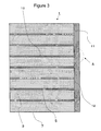
- a porous layer 13 composed of a conductor layer having a plurality of pores, for example, may be arranged as illustrated in Fig. 3 .
- the porous layer 13 has a strength lower than the strength of the internal electrode layers 5, and cracks are easily formed in the porous layer 13 by a stress. Accordingly, breaking of the porous layer 13 due to cracks or the like is caused by a stress generated in the laminate 7 during driving prior to the breaking of the internal electrode layers 5.
- the porous layer 13 functions as a layer that relieves a stress in the laminate 7.
- the porous layer 13 is provided in the laminate 7 and a plurality of pores are present between the porous layer 13 and the inorganic material layer 11 (a plurality of pores are located on the side of the porous layer 13).
- the cracks can be selectively induced to a region of the inorganic material layer 11 located on the side of the porous layer 13. Accordingly, cracks are not formed in a region of the inorganic material layer 11 located on the side of an internal electrode layer 5 (region facing an end of an internal electrode layer 5), and thus electrical discharges on the surface of the inorganic material layer 11 can be suppressed.
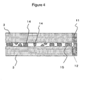
- the porous layer 13 is mainly composed of metal particles separated with gaps therebetween, and particles 15 composed of the same material as the inorganic material layer 11 are present in the porous layer 13.
- a stress having a high impact velocity can be absorbed by distortion of a crystal lattice of the particles 15 composed of the same material of the inorganic material layer 11, and a stress having a low impact velocity but having a high impact strength can be absorbed by deformation of the shapes of the metal particles 14.
- the metal particles 14 each have a particle diameter of 0.1 to 50 ⁇ m, for example. This value can be determined by observing a cross section with an electron microscope such as a scanning electron microscope (SEM) or a metallurgical microscope, measuring the number of spaces between particles included in an arbitrary line segment and the distances between the particles, measuring the number of particles included in the arbitrary line segment and the length of the line segment included in each of the particles, and dividing the total of the length of the line segment by the number of particles.
- SEM scanning electron microscope
- the distance formed by the gap between the metal particles 14 is 1 to 100 ⁇ m, for example. This value can be determined by observing a cross section with an electron microscope such as a scanning electron microscope (SEM) or a metallurgical microscope, measuring the number of spaces between particles included in an arbitrary line segment and the distances between the particles, and dividing the total of the distance between the particles by the number of spaces between the particles.
- SEM scanning electron microscope
- the particles 15 composed of the same material as the inorganic material layer 11 and present in the porous layer 13 have a size of 0.05 to 50 ⁇ m, for example, and are preferably scattered.
- the phrase "the particles 15 are scattered in the porous layer 13" means that when a cross section is observed with an electron microscope such as a scanning electron microscope (SEM) or a metallurgical microscope, a plurality of particles 15 are dispersed together with the metal particles 14 with gaps therebetween.
- a particle 15 composed of the same material as the inorganic material layer 11 so as to contact a pore 12 located between the porous layer 13 and the inorganic material layer 11, a stress-absorbing effect similar to that in the porous layer 13 is generated in a region of the inorganic material layer 11 located on the side of the porous layer 13, and a stress of the laminate 7 can be relieved.
- the cracks are formed in the particles 15 composed of the same material as the inorganic material layer 11 and, at the same time, the cracks can be selectively induced to a region of the inorganic material layer 11 located on the side of the porous layer 13.
- the particles 15 are continuously broken along the porous layer 13, whereby the cracks can be induced to the inorganic material layer 11 in a direct line.
- the cracks are not formed in a region of the inorganic material layer 11, the region facing an end of an internal electrode layer 5, and thus electrical discharges on the surface of the inorganic material layer 11 can be suppressed.
- piezoelectric green sheets to be formed into piezoelectric layers 3 are prepared. Specifically, a calcined powder of a piezoelectric ceramic, a binder composed of an organic polymer such as an acrylic polymer or a butyral polymer, and a plasticizer are mixed to prepare a ceramic slurry. Then, piezoelectric green sheets are prepared by a tape forming method such as a doctor blade method or a calender roll method using the ceramic slurry. Any piezoelectric ceramic that exhibits piezoelectricity can be used.
- Examples thereof includes perovskite-type oxides such as lead zirconate titanate (PZT: PbZrO 3 -PbTiO 3 ), lithium niobate (LiNbO 3 ), and lithium tantalate (LiTaO 3 ).
- the plasticizer include dibutyl phthalate (DBP) and dioctyl phthalate (DOP).
- an internal electrode paste to be formed into internal electrode layers 5 is prepared. Specifically, for example, a binder and a plasticizer are added to and mixed with a metal powder composed of a silver-palladium (Ag-Pd) alloy to prepare an internal electrode paste. Alternatively, a silver powder and a palladium powder may be mixed instead of using the silver-palladium alloy.
- a binder and a plasticizer are added to and mixed with a metal powder composed of a silver-palladium (Ag-Pd) alloy to prepare an internal electrode paste.
- a silver powder and a palladium powder may be mixed instead of using the silver-palladium alloy.
- the internal electrode paste is applied onto the piezoelectric green sheets so as to form a pattern of the internal electrode layers 5 by a screen printing method, for example.
- a conductive paste for a porous layer in order to form a plurality of pores in a conductor layer functioning as the porous layer, a conductive paste for a porous layer, the conductive paste containing a substance that is removed or evaporated during firing, e.g., acrylic beads or the like, is prepared, and the conductive paste is applied by a screen printing method.
- the pattern of the porous layer may be formed over the entire surface of a cross section perpendicular to the stacking direction of a laminate 7, or may be formed as a partial pattern.
- the pattern is preferably formed as a pattern in which the external electrodes 8 functioning as a positive electrode and a negative electrode are divided by a non-forming portion.
- a predetermined number of the piezoelectric green sheets having the internal electrode paste thereon are stacked to prepare a laminated formed body.
- a columnar laminated formed body is prepared in which a plurality of piezoelectric green sheets and a plurality of internal electrode paste layers are alternately stacked and some end faces of the internal electrode paste layers reach side faces of the laminated formed body.
- Piezoelectric green sheets on which the conductive paste for a porous layer is applied may be stacked at predetermined intervals (with a predetermined number of piezoelectric green sheets therebetween).
- the laminated formed body may be prepared by arranging, on each of the top and the bottom of the laminated formed body, a piezoelectric green sheet that does not have the conductive paste thereon.
- an inorganic material paste to be formed into an inorganic material layer 11 is applied onto side faces of the laminated formed body to which end faces of the internal electrode paste layers extend so as to cover the end faces of the internal electrode layers 5.
- the inorganic material paste is prepared by mixing an inorganic material powder, a solvent, and a binder. Subsequently, a uniform film is formed on the side faces of the laminated formed body by a method such as screen printing, dipping, or dispenser coating.
- the inorganic material paste is applied onto an area other than an area where an external electrode paste described below is to be applied.
- a binder such as ethyl cellulose, containing a solid material, such as acrylic beads, a carbon powder, or the like, which is removed or evaporated during firing is preferably applied onto the side faces of the laminated formed body before the inorganic material paste to be formed into the inorganic material layer 11 is applied.
- a solid material such as acrylic beads or a carbon powder
- pores having a diameter of, for example, about 0.3 to 1.5 ⁇ m can be formed in a uniformly dispersed manner at the interface between the side faces of the laminate 7 and the inorganic material layer 11. Furthermore, by adjusting the proportion of the acrylic beads, the carbon powder, or the like, the abundance ratio (distribution) of the pores can be controlled.
- the binder containing a solid material that is removed or evaporated during firing is applied not over the entire side faces of the laminate 7 but partially applied, whereby the pores 12 can be formed at positions between the internal electrode layers 5 or in the central portion of the laminate 7 in the stacking direction. Furthermore, by applying the solid material (such as acrylic beads or a carbon powder) which is removed or evaporated during firing so that the proportion of the solid material is made different in different portions, the abundance ratio (distribution) of the pores can be adjusted.
- portions where the application of the binder is unnecessary for example, regions located on the side faces of the internal electrode layers
- the application may be performed a plurality of times for various masking portions.
- a binder such as ethyl cellulose containing a solid material that is removed or evaporated during firing is applied onto side faces of the laminated formed body.
- a solid material such as acrylic beads or a carbon powder
- the inorganic material paste may be mixed with the inorganic material paste to be formed into the inorganic material layer 11 to the extent that cracks are not formed in the inorganic material layer 11 so that the advantages of the present invention are not impaired, and thus the pores 12 may be formed at an interface between the side faces of the laminate 7 and the inorganic material layer 11.
- a binder such as ethyl cellulose, containing acrylic beads, a carbon powder, or the like is applied onto a side face of the laminated formed body, or the laminated formed body is immersed in a container containing the binder.
- the laminated formed body in this state is placed in a container such as a desiccator, and the pressure in the container is reduced to 0.1 atm (about 10 kPa) with a vacuum pump.
- the acrylic beads, the carbon powder, or the like can be infiltrated in the porous layer 13 together with the binder.
- the inorganic material paste is applied, and the resulting laminated formed body is then fired.
- a plurality of pores can be formed between the porous layer 13 and the inorganic material layer 11.
- the porous layer 13 which is mainly composed of metal particles separated with gaps therebetween, and in which particles 15 composed of the same material as the inorganic material layer 11 are scattered therein
- a binder such as ethyl cellulose, containing acrylic beads, a carbon powder, or the like is applied onto a side face of the laminated formed body, or the laminated formed body is immersed in a container containing the binder.
- the laminated formed body in this state is placed in a container such as a desiccator, and the pressure in the container is reduced to 0.1 atm (about 10 kPa) with a vacuum pump.
- the acrylic beads, the carbon powder, or the like is infiltrated in the porous layer 13 together with the binder.
- the inorganic material paste is applied, and the resulting laminated formed body is then again placed in the container such as a desiccator, and the pressure in the container is reduced to 0.1 atm (about 10 kPa) with a vacuum pump so that the components of the inorganic material paste are dispersed in the porous layer 13.
- the laminated formed body is then fired to obtain the porous layer 13.
- the porous layer 13 can be also obtained by applying the inorganic material paste is applied without applying acrylic beads, a carbon powder, or the like in advance, placing the resulting laminated formed body in a container such as a desiccator to reduce the pressure therein to 0.1 atm (about 10 kPa) with a vacuum pump so that the components of the inorganic material paste are dispersed in the porous layer 13, and by firing the laminated formed body.
- a container such as a desiccator to reduce the pressure therein to 0.1 atm (about 10 kPa) with a vacuum pump so that the components of the inorganic material paste are dispersed in the porous layer 13, and by firing the laminated formed body.
- the laminated formed body on which the inorganic material paste is applied is subjected to a debinding treatment at a determined temperature, and is then fired at a temperature in a range of 900°C to 1,200°C to prepare a columnar laminate 7 in which the piezoelectric layers 3 and the internal electrode layers 5 are alternately stacked and the inorganic material layer 11 adheres to the side faces of the laminate 7.
- a polishing process is performed on side faces of the laminate 7 obtained by firing. Specifically, a pair of regions of the inorganic material layer 11 is partly removed so as to extend in the stacking direction of the laminate 7, thus alternately exposing end faces of the internal electrode layers 5.
- the side faces of the laminate 7 are ground in a direction parallel to the internal electrode layers 5 with a surface grinder or a polygon machine using a grindstone having a grain size of #200 to #1000 until the laminate 7 has a predetermined shape.
- the amount of cut of the grindstone is reduced to preferably 50 ⁇ m or less and more preferably 5 ⁇ m or less, and a polishing process is performed a plurality of times (preferably three times or more).
- the external electrode paste is printed as a pattern of the external electrodes 8 so as to cover the regions where the internal electrode layers 5 are exposed, and is then baked at 650°C to 750°C to form the external electrodes 8.
- the external electrode paste for example, a silver glass conductive paste containing silver as a main component and glass is preferred.
- the method for forming the inorganic material layer 11 and the external electrodes 8 includes, instead of steps of: applying an inorganic material paste onto side faces of a laminated formed body at which end faces of internal electrode paste layers are exposed so as to cover the side faces; firing the laminated formed body having the inorganic material paste thereon to obtain a columnar laminate in which piezoelectric layers and internal electrode layers are alternately stacked and an inorganic material layer adheres to side faces; partly removing a pair of regions of the inorganic material layer, the regions extending in a stacking direction of the laminate, to alternately expose the internal electrode layers; and applying an external electrode paste so as to cover the regions where the internal electrode layers are exposed, steps of: applying an inorganic material paste onto side faces of a laminated formed body at which end faces of internal electrode paste layers are exposed, the side faces not including regions where an external electrode paste is to be applied, so as to cover the side faces; firing the laminated formed body having the inorganic material paste thereon to obtain a columnar laminate in which piezo
- external lead members 9 are connected and fixed to the surfaces of the external electrodes 8 with a conductive bonding material (solder) 10 therebetween.
- a direct current electric field of 0.1 to 3 kV/mm is applied from the external lead members 9 connected to the pair of external electrodes 8 to the piezoelectric layers 3 through the external electrodes 8 and the internal electrode layers 5 to polarize the piezoelectric layers 3 of the laminate 7.
- a multilayer piezoelectric element 1 is produced.
- Each of the piezoelectric layers 3 of this multilayer piezoelectric element 1 can be significantly displaced due to the inverse piezoelectric effect by connecting the external electrodes 8 to an external power supply through the external lead members 9 and applying a driving voltage to the piezoelectric layers 3 through the internal electrode layers 5.
- the multilayer piezoelectric element 1 can function as, for example, a fuel injection valve for an automobile, which injects and supplies fuel to an engine.
- Examples of the applications of the multilayer piezoelectric element 1 of this embodiment include piezoelectric drive elements (piezoelectric actuators), pressure sensor elements, and piezoelectric circuit elements.
- Examples of the piezoelectric drive elements include a fuel injection device of an automobile engine, a liquid ejection device such as an ink jet, a precise positioning device such as an optical device, and a vibration control device.
- Examples of the pressure sensor element include a combustion pressure sensor, a knocking sensor, an acceleration sensor, a load sensor, an ultrasonic sensor, a pressure sensor, and a yaw rate sensor.
- Examples of the piezoelectric circuit element include a piezoelectric gyro, a piezoelectric switch, a piezoelectric transducer, and a piezoelectric breaker.
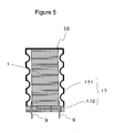
- FIG. 5 is a schematic cross-sectional view illustrating a piezoelectric actuator according to an embodiment of the present invention.
- a multilayer piezoelectric element 1 is contained in a case 17.
- the case 17 includes a case body 171 having a closed upper end and an open lower end, and a cover 172 that is attached to the case body 171 so as to cover the opening of the case body 171.
- the multilayer piezoelectric element 1 is enclosed in the case 17 with, for example, an inert gas so that end faces of the multilayer piezoelectric element 1 contact the inner wall of the upper end and inner wall of the lower end of the case 17.
- the case body 171 and the cover 172 are each composed of a metal material such as SUS 304 or SUS 316L.
- the case body 171 is a cylinder having a closed upper end and an open lower end, and has, for example, a bellows shape so that the case body 171 can be expanded and contracted in the stacking direction of a laminate 7.
- the cover 172 has, for example, a plate shape so as to cover the opening of the case body 171.
- Two through-holes for inserting external lead members 9 are formed in the cover 172.
- the external lead members 9 are inserted in the through-holes so that external electrodes 8 and the outside are electrically connected to each other. Gaps of the through-holes are filled with soft glass or the like, thereby fixing the external lead members 9 and preventing infiltration of outside air.
- each of the piezoelectric layers 3 can be largely displaced due to the inverse piezoelectric effect by connecting to an external power supply through the external lead members 9 and applying a driving voltage to the piezoelectric layers 3 through the internal electrode layers 5.
- the multilayer piezoelectric element can function as a piezoelectric actuator and can be stably driven for a long period of time.
- FIG. 6 is a schematic cross-sectional view illustrating an injection device according to an embodiment of the present invention.
- the multilayer piezoelectric element 1 described in the above embodiment is contained inside a housing (case) 23 having an injection hole 21 at an end thereof.
- a needle valve 25 that can open and close the injection hole 21 is provided in the housing 23.
- a fluid path 27 is provided so as to communicate with the injection hole 21 in accordance with the movement of the needle valve 25.
- the fluid path 27 is connected to an external fluid supply source, and a fluid is constantly supplied to the fluid path 27 at a high pressure. Accordingly, when the needle valve 25 opens the injection hole 21, the fluid supplied to the fluid path 27 is discharged from the injection hole 21 to the outside or to an adjacent container, for example, a combustion chamber (not illustrated) of an internal-combustion engine.
- An upper end of the needle valve 25 has a large inner diameter, and a cylinder 29 formed in the housing 23 and a slidable piston 31 are arranged on the upper end of the needle valve 25.
- the multilayer piezoelectric element 1 of the present invention described in the above embodiment is contained in the housing 23.
- the injection device 19 of this embodiment may include a container 23 having an injection hole 21 and the multilayer piezoelectric element 1 described in the above embodiment, wherein a fluid charged in the container 23 is discharged from the injection hole 21 by driving the multilayer piezoelectric element 1. That is, the multilayer piezoelectric element 1 need not be provided in the container 23, and it is sufficient that a pressure for controlling the injection of the fluid is applied to the inside of the container 23 by driving the multilayer piezoelectric element 1.
- the term "fluid" refers to not only fuel, an ink, and the like but also various types of gas and liquid such as a conductive paste. The flow rate and injection timing of a fluid can be stably controlled for a long period of time by using the injection device 19 of this embodiment.
- fuel can be stably injected to a combustion chamber of an internal-combustion engine such as an engine with high accuracy for a longer period of time, as compared with known injection devices.
- FIG. 7 is a schematic view illustrating a fuel injection system according to an embodiment of the present invention.
- a fuel injection system 35 of this embodiment includes a common rail 37 that stores high-pressure fuel as a high-pressure fluid, a plurality of injection devices 19 that are described in the above embodiment and that inject the high-pressure fluid stored in the common rail 37, a pressure pump 39 that supplies the high-pressure fluid to the common rail 37, and an injection control unit 41 that provides a driving signal to the injection devices 19.
- the injection control unit 41 controls the amount and timing of the injection of the high-pressure fluid on the basis of external information or a signal from the outside.
- the amount and timing of the fuel injection can be controlled while sensing the state in a combustion chamber of the engine with a sensor or the like.
- the pressure pump 39 has a function of supplying fluid fuel from a fuel tank 43 to the common rail 37 at a high pressure.
- the fluid fuel is fed to the common rail 37 at a high pressure of about 1,000 to 2,000 atm (about 101 MPa to about 203 MPa), and preferably about 1,500 to 1,700 atm (about 152 MPa to about 172 MPa).
- the common rail 37 stores the high-pressure fuel supplied from the pressure pump 39 and appropriately feeds the high-pressure fuel to the injection devices 19.
- Each of the injection devices 19 injects a certain amount of fluid from the injection hole 21 to the outside or to an adjacent container as described above.
- high-pressure fuel is injected from the injection hole 21 to a combustion chamber of the engine in the form of a mist.
- the present invention is not limited to the above embodiments, and various changes can be made without departing from the gist of the present invention.
- the external electrodes 8 in the multilayer piezoelectric element 1 are formed on two opposite side faces of the laminate 7.
- two external electrodes 8 may be formed on adjacent side faces of the laminate 7, or on the same side face of the laminate 7.
- the shape of a cross section of the laminate 7 in a direction orthogonal to the stacking direction may be, instead of a quadrangular shape in the above embodiment, a polygonal shape such as a hexagonal shape or an octagonal shape, a circular shape, or a shape formed by combining straight lines and circular arcs.
- a piezoelectric actuator including a multilayer piezoelectric element of the present invention was prepared as follows. First, a calcined powder of a piezoelectric ceramic containing, as a main component, lead zirconate titanate (PZT: PbZrO 3 -PbTiO 3 ) and having an average particle diameter of 0.4 ⁇ m, a binder, and a plasticizer were mixed to prepare a ceramic slurry. Ceramic green sheets to be formed into piezoelectric layers 3, the ceramic green sheets each having a thickness of 100 ⁇ m, were prepared by a doctor blade method using the ceramic slurry. A conductive paste to be formed into internal electrode layers was prepared by adding a binder to a silver-palladium alloy.
- PZT lead zirconate titanate
- the conductive paste to be formed into internal electrode layers was printed on one surface of each of the ceramic green sheets by a screen printing method. Then, the 300 ceramic green sheets on which the conductive paste was printed were stacked to prepare a laminated formed body.
- the laminate was ground so as to have a predetermined shape using a surface grinder. Furthermore, a pair of regions of the inorganic material layer was partly removed so as to extend in the stacking direction of the laminate, thus alternately exposing end faces of the internal electrode layers.
- an external electrode paste containing silver as a main component and glass was printed on the side faces to which the internal electrode layers of the laminate were led.
- the external electrode paste was baked at 650°C to 750°C to form external electrodes.
- Multilayer piezoelectric elements were prepared as described above.
- multilayer piezoelectric elements samples having different proportions of the pores were prepared. Specifically, a multilayer piezoelectric element (sample No. 1) in which pores were uniformly distributed (in a proportion of 10%) in the stacking direction in cross-sectional view, a multilayer piezoelectric element (sample No. 2) in which pores were present, in cross-sectional view, in a proportion of 20% between all the internal electrode layers and in a proportion of 10% in regions located on the side faces of the internal electrode layers, a multilayer piezoelectric element (sample No.
- sample No. 1 was prepared by applying a binder having an acrylic bead content of 10%.
- Sample No. 2 was prepared by masking regions between the internal electrode layers and applying a binder having an acrylic bead content of 10% onto regions located on the side faces of the internal electrode layers, and then masking the regions located on the side faces of the internal electrode layers and applying a binder having an acrylic bead content of 20% onto the regions between the internal electrode layers.
- Sample No. 3 was prepared by masking regions other than a central portion and applying a binder having an acrylic bead content of 20% onto only the central portion, and then masking the central portion (central portion when the laminate was divided into three equal parts in the stacking direction) and applying a binder having an acrylic bead content of 10% onto other regions.
- a cross section of each of the prepared multilayer piezoelectric elements cut in the stacking direction was observed with a scanning electron microscope to measure the average diameter of the pores.
- the average diameter of the pores was 2.2 ⁇ m.
- the cross section of each of the multilayer piezoelectric elements cut in the stacking direction was observed with a scanning electron microscope, and the proportion of the pores in a predetermined distance was determined. It was confirmed that the proportions of the pores were the values described above.
- the prepared multilayer piezoelectric elements were electrically driven for 1 ⁇ 10 8 cycles.
- the multilayer piezoelectric element (sample No. 4), which had no pores, a short-circuit occurred.
- sample Nos. 1 to 3 which had pores, the generation of a short-circuit was not observed.
Landscapes
- Engineering & Computer Science (AREA)
- Manufacturing & Machinery (AREA)
- Fuel-Injection Apparatus (AREA)
- Particle Formation And Scattering Control In Inkjet Printers (AREA)
Abstract
Description
- The present invention relates to a multilayer piezoelectric element used as a piezoelectric drive element (piezoelectric actuator), a pressure sensor element, a piezoelectric circuit element, or the like, a method for producing the same, an injection device including the multilayer piezoelectric element, and a fuel injection system.
- A known multilayer piezoelectric element includes a columnar laminate in which a plurality of piezoelectric layers and a plurality of internal electrode layers are alternately stacked and some of end faces of the internal electrode layers are exposed at side faces of the laminate, and a pair of external electrodes which adhere to the side faces of the laminate so as to extend in a stacking direction and to which alternating ones of the internal electrode layers are respectively electrically connected.
- It is also known that an organic (resin) covering layer is formed on the side faces of a laminate to electrically and mechanically protect the laminate (refer to, for example, Patent Document 1).
-
- Patent Document 1: Japanese Unexamined Patent Application Publication No.
4-259268 - Here, the covering layer has a function of suppressing the generation of electrical discharges (short-circuits) between a positive electrode and a negative electrode in the multilayer piezoelectric element or between the multilayer piezoelectric element and a metal case that encloses the multilayer piezoelectric element. An organic (resin) covering layer can conform to the expansion and contraction of the laminate as compared with an inorganic covering layer. Thus, the formation of an organic (resin) covering layer is advantageous in that a stress can be relieved.
- However, the adhesion of such an organic (resin) covering layer tends to be decreased by thermal degradation due to long-term driving. Specifically, even when an organic (resin) covering layer is formed in close contact with the laminate, the covering layer tends to become separated from the laminate during long-term driving. As a result, a gap is formed by this separation between the laminate and the covering layer and this gap causes a short-circuit. Consequently, there may be a problem that the driving of the multilayer piezoelectric element becomes unstable or stops.
- The present invention has been made in view of the above circumstances, and an object of the present invention is to provide a multilayer piezoelectric element including a covering layer that can relieve a stress generated by expansion and contraction of a laminate and that is not easily separated even during long-term driving, a method for producing the multilayer piezoelectric element, an injection device including the multilayer piezoelectric element, and a fuel injection system.
- A multilayer piezoelectric element of the present invention includes a columnar laminate in which a plurality of piezoelectric layers and a plurality of internal electrode layers are stacked and some of end faces of the internal electrode layers reach side faces of the laminate; a pair of external electrodes adhering to the side faces of the laminate so that alternating ones of the internal electrode layers are respectively electrically connected to the external electrodes; and an inorganic material layer adhering to the side faces of the laminate so as to cover the end faces of the internal electrode layers in regions where at least the pair of external electrodes is not provided, wherein pores are present between the inorganic material layer and the side faces of the laminate.
- A piezoelectric actuator of the present invention includes the multilayer piezoelectric element of the present invention and a case that contains the multilayer piezoelectric element therein.
- An injection device of the present invention includes a container having an injection hole and the multilayer piezoelectric element of the present invention, wherein a fluid stored in the container is discharged from the injection hole by driving the multilayer piezoelectric element.
- A fuel injection system of the present invention includes a common rail that stores high-pressure fuel, the injection device of the present invention that injects the high-pressure fuel stored in the common rail, a pressure pump that supplies the high-pressure fuel to the common rail, and an injection control unit that provides a driving signal to the injection device.
- According to the multilayer piezoelectric element of the present invention, the covering layer for suppressing short-circuits is a highly heat-resistant inorganic material layer. Thus, even when the multilayer piezoelectric element is exposed to a high temperature for a long period of time, the covering layer is not easily degraded, and a strong bonding strength (adhesion) between the covering layer and piezoelectric layers can be obtained. In addition, since the inorganic material layer has good solvent resistance, driving of the multilayer piezoelectric element in liquid can also be realized. Furthermore, since a large number of pores are present between the inorganic material layer and side faces of the laminate, a stress generated (at an interface) between the inorganic material layer and the laminate during driving can be effectively relieved. Furthermore, the pores delay the transmission of heat generated in the laminate, thereby preventing the inorganic material layer from becoming separated by expansion thereof due to a rapid increase in heat.
-
- [
Fig. 1] Fig. 1 is a perspective view illustrating a multilayer piezoelectric element according to an embodiment of the present invention. - [
Fig. 2] Fig. 2 is a partial, enlarged, cross-sectional view in a cross section (cross section that cuts across an inorganic material layer) parallel to a stacking direction of the multilayer piezoelectric element illustrated inFig. 1 . - [
Fig. 3] Fig. 3 illustrates a multilayer piezoelectric element according to another embodiment of the present invention, and is a partial, enlarged, cross-sectional view in a cross section (cross section that cuts across an inorganic material layer) parallel to a stacking direction. - [
Fig. 4] Fig. 4 is an enlarged view of region A including an inorganic material layer and a porous layer illustrated inFig. 3 . - [
Fig. 5] Fig. 5 is a schematic cross-sectional view illustrating a piezoelectric actuator according to an embodiment of the present invention. - [
Fig. 6] Fig. 6 is a schematic cross-sectional view illustrating an injection device according to an embodiment of the present invention. - [
Fig. 7] Fig. 7 is a schematic view illustrating a fuel injection system according to an embodiment of the present invention. - Embodiments of a multilayer piezoelectric element of the present invention will now be described in detail with reference to the drawings.
-
Fig. 1 is a perspective view illustrating a multilayer piezoelectric element according to an embodiment of the present invention.Fig. 2 is a partial, enlarged, cross-sectional view in a cross section (cross section that cuts across an inorganic material layer) parallel to a stacking direction of the multilayer piezoelectric element illustrated inFig. 1 . - As illustrated in
Figs. 1 and2 , a multilayerpiezoelectric element 1 of the embodiment includes alaminate 7 in which a plurality ofpiezoelectric layers 3 and a plurality ofinternal electrode layers 5 are stacked and some of end faces of theinternal electrode layers 5 reach side faces of thelaminate 7. In addition, on the side faces of thelaminate 7, a pair ofexternal electrodes 8 respectively electrically connected to alternating ones of theinternal electrode layers 5. In regions where at least the pair ofexternal electrodes 8 is not provided, aninorganic material layer 11 adheres to the side face of thelaminate 7 so as to cover the end faces of theinternal electrode layers 5. The multilayerpiezoelectric element 1 haspores 12 between theinorganic material layer 11 and the side face of thelaminate 7. - The
laminate 7 illustrated inFigs. 1 and2 includes an active portion in which thepiezoelectric layers 3 and theinternal electrode layers 5 are alternately stacked and inactive portions disposed on both ends of the active portion and each including apiezoelectric layer 3. Some of end faces of theinternal electrode layers 5 reach side faces of thelaminate 7, and the end faces each include a portion that is electrically connected to theexternal electrode 8 and a portion that is covered with theinorganic material layer 11. - The
piezoelectric layers 3 forming thelaminate 7 are composed of a piezoelectric porcelain (piezoelectric ceramic) that exhibits piezoelectricity. The piezoelectric porcelain forming thepiezoelectric layers 3 is formed to have an average grain size of, for example, 1.6 to 2.8 µm. Examples of the piezoelectric porcelain that can be used include perovskite-type oxides such as PbZrO3-PbTiO3 (PZT: lead zirconate titanate), lithium niobate (LiNbO3), and lithium tantalate (LiTaO3), and the like. Thelaminate 7 illustrated inFig. 1 has a quadrangular column shape. Alternatively, thelaminate 7 may have, for example, a hexagonal column shape, an octagonal column shape, or the like. - The
internal electrode layers 5 are alternately stacked with thepiezoelectric layers 3 so as to sandwich each of thepiezoelectric layers 3 in the vertical direction. A positive electrode and a negative electrode are arranged in the order of stacking so that a driving voltage is applied to apiezoelectric layer 3 interposed therebetween. Theinternal electrode layers 5 are composed of a metal such as a silver-palladium (Ag-Pd) alloy, copper, or platinum. In this embodiment, positive electrodes and negative electrodes (or ground electrodes) are alternately led to opposite side faces of thelaminate 7, and portions of end faces of theinternal electrode layers 5 are electrically connected to the pair ofexternal electrodes 8 bonded to the side faces of thelaminate 7. - The pair of
external electrodes 8 is formed by applying a paste containing, for example, silver and glass and baking the paste, and adheres to opposite side faces of the laminate 2 so as to extend in the stacking direction. Theexternal electrodes 8 are electrically connected to theinternal electrode layers 5 that are alternately led to the opposite side faces of thelaminate 7. InFig. 1 , theexternal electrode 8 is formed so that the width of theexternal electrode 8 is smaller than the width of the surface on which theexternal electrode 8 is formed. Alternatively, the width of theexternal electrode 8 and the width of the surface may be the same. In particular, in the case where thelaminate 7 has a hexagonal column shape or an octagonal column shape, theexternal electrode 8 may be formed such that the width of theexternal electrode 8 is the same as the width of the surface having theexternal electrode 8 thereon. - The
inorganic material layer 11 adhering to the side faces of thelaminate 7 so as to cover end faces of theinternal electrode layers 5 in regions where at least the pair ofexternal electrodes 8 is not provided is formed so as to have a thickness of, for example, several micrometers to several hundred micrometers and strongly bonded to thelaminate 7. Examples of the material of theinorganic material layer 11 include piezoelectric materials, glass, and alumina. In particular, a piezoelectric material same as the piezoelectric porcelain forming thepiezoelectric layers 3, for example, PbZrO3-PbTiO3 (PZT: lead zirconate titanate) is preferably used. By forming theinorganic material layer 11 using a piezoelectric material (preferably, a piezoelectric material the same as the piezoelectric porcelain forming the piezoelectric layers 3), not only driving in liquid or in high humidity can be realized but also theinorganic material layer 11 exhibits the piezoelectric effect due to a leakage electric field (electric field generated in an area that is not sandwiched between electrodes) from theinternal electrode layers 5 and can conform to expansion and contraction of the element. Herein, the phrase "adhering to the side faces of thelaminate 7 so as to cover end faces of theinternal electrode layers 5 in regions where at least the pair ofexternal electrodes 8 is not provided" refers to the following. Among side faces of thelaminate 7 to which some of end faces of theinternal electrode layers 5 extend, in the case where side faces havingexternal electrodes 8 thereon include areas where the end faces of theinternal electrode layers 5 are not covered with theexternal electrodes 8, theinorganic material layer 11 adheres to the areas. Furthermore, as illustrated inFig. 1 , in the case where some of end faces of theinternal electrode layers 5 reach side faces other than the side faces having theexternal electrodes 8 thereon, theinorganic material layer 11 may adhere to the side faces that do not have theexternal electrodes 8 thereon. Theinorganic material layer 11 does not cover the end faces of theinternal electrode layers 5 covered with theexternal electrode 8. However, for example, theinorganic material layer 11 may be formed so that a part of theinorganic material layer 11 is interposed between a side face of thelaminate 7 and theexternal electrode 8 so as to overlap with a peripheral edge portion of theexternal electrode 8. - The plurality of
pores 12 present between theinorganic material layer 11 and a side face of thelaminate 7 each have a diameter of, for example, 0.3 to 1.5 µm. Thepores 12 are formed so that, in cross-sectional view, the total of portions of thepores 12, the portions being in contact with the side face of thelaminate 7, is, for example, 1% to 40% and preferably 10% to 20% relative to the length of the side face of thelaminate 7. The presence of the plurality of (large number of) pores 12 can effectively relieve a stress (at an interface) between theinorganic material layer 11 and thelaminate 7 generated during driving. - In addition, the
pores 12 disturb transmission of heat generated in thelaminate 7, thereby preventing theinorganic material layer 11 from becoming separated by expansion thereof due to a rapid increase in heat. The multilayerpiezoelectric element 1 generates heat by expansion and contraction thereof. For example, in the case where theinorganic material layer 11 is a covering material composed of a resin instead of an inorganic material, this heat causes thermal degradation of the covering material. On the other hand, in the case where the coveting material is theinorganic material layer 11, since theinorganic material layer 11 has good thermal conductivity, rapid thermal expansion of theinorganic material layer 11 occurs, and theinorganic material layer 11 may be separated. In contrast, since the large number ofpores 12, which have poor thermal conductivity, are present between theinorganic material layer 11 and the side faces of thelaminate 7, transmission of heat is disturbed, thereby preventing theinorganic material layer 11 from becoming separated by expansion thereof due to a rapid increase in heat. - The plurality of
pores 12 are preferably located on the side of the piezoelectric layers 3 (located between the internal electrode layers 5) rather than on the side of the internal electrode layers 5. In other words, thepores 12 are preferably located between any of thepiezoelectric layers 3 and theinorganic material layer 11. Thepiezoelectric layers 3 are expanded and contracted by driving the multilayerpiezoelectric element 1. Therefore, in the case where thepores 12 are located between any of thepiezoelectric layers 3 and theinorganic material layer 11, the stress generated by the expansion and contraction of the piezoelectric layers can be more effectively relieved. The above multilayerpiezoelectric element 1 has a structure in which thepores 12 are not present in regions located between any of theinternal electrode layers 5 and theinorganic material layer 11 but are present only between any of thepiezoelectric layers 3 and theinorganic material layer 11. However, the structure is not limited thereto. Alternatively, the multilayerpiezoelectric element 1 may have a structure in which the abundance ratio of thepores 12 located between thepiezoelectric layers 3 and theinorganic material layer 11 is higher than the abundance ratio of thepores 12 located between theinternal electrode layers 5 and theinorganic material layer 11. - The
pores 12 are preferably located in the active portion in which thepiezoelectric layers 3 and theinternal electrode layers 5 are alternately stacked. In particular, in the multilayerpiezoelectric element 1 of this embodiment, thepores 12 are preferably located in a central portion of thelaminate 7 in the stacking direction. The central portion of thelaminate 7 in the stacking direction is largely expanded and contracted, as compared with end portions of thelaminate 7 in the stacking direction. Therefore, in the case where thepores 12 are located in the central portion of thelaminate 7 in the stacking direction, a stress can be more effectively relieved. The term "central portion" refers to a central portion when thelaminate 7 is divided into three equal parts in the stacking direction. The multilayerpiezoelectric element 1 has a structure in which thepores 12 are present only in the central portion, and are not present in other portions. However, the structure is not limited thereto. Alternatively, the multilayerpiezoelectric element 1 may have a structure in which the abundance ratio of thepores 12 located in the central portion is higher than the abundance ratios of thepores 12 located in other portions. - The size of each of the
pores 12 is preferably smaller than the average grain size of the piezoelectric porcelain forming thepiezoelectric layers 3. In this case, a stress can be relieved in a more dispersed manner while ensuring insulating properties. The average size of thepores 12 and the average grain size of the piezoelectric porcelain are determined by polishing the multilayerpiezoelectric element 1 in a side face direction, and observing the polished multilayerpiezoelectric element 1 with an electron microscope. - Furthermore, the
inorganic material layer 11 is preferably composed of a piezoelectric material. In this case, the inorganic material layer exhibits the piezoelectric effect by a leakage electric field and can conform to expansion and contraction of the element. Thus, the element can be stably driven for a longer period of time. In particular, from the standpoint of the bonding strength, theinorganic material layer 11 and thepiezoelectric layers 3 are preferably composed of the same piezoelectric material. - In the
laminate 7, in place of some of the plurality ofinternal electrode layers 5, aporous layer 13 composed of a conductor layer having a plurality of pores, for example, may be arranged as illustrated inFig. 3 . Theporous layer 13 has a strength lower than the strength of theinternal electrode layers 5, and cracks are easily formed in theporous layer 13 by a stress. Accordingly, breaking of theporous layer 13 due to cracks or the like is caused by a stress generated in thelaminate 7 during driving prior to the breaking of the internal electrode layers 5. Thus, theporous layer 13 functions as a layer that relieves a stress in thelaminate 7. - As just described, the
porous layer 13 is provided in thelaminate 7 and a plurality of pores are present between theporous layer 13 and the inorganic material layer 11 (a plurality of pores are located on the side of the porous layer 13). In this case, even if cracks are formed in theporous layer 13 when theporous layer 13 relieves a stress of thelaminate 7, the cracks can be selectively induced to a region of theinorganic material layer 11 located on the side of theporous layer 13. Accordingly, cracks are not formed in a region of theinorganic material layer 11 located on the side of an internal electrode layer 5 (region facing an end of an internal electrode layer 5), and thus electrical discharges on the surface of theinorganic material layer 11 can be suppressed. - As illustrated in
Fig. 4 , preferably, theporous layer 13 is mainly composed of metal particles separated with gaps therebetween, andparticles 15 composed of the same material as theinorganic material layer 11 are present in theporous layer 13. With this structure, among stresses applied to theporous layer 13, a stress having a high impact velocity can be absorbed by distortion of a crystal lattice of theparticles 15 composed of the same material of theinorganic material layer 11, and a stress having a low impact velocity but having a high impact strength can be absorbed by deformation of the shapes of themetal particles 14. - The
metal particles 14 each have a particle diameter of 0.1 to 50 µm, for example. This value can be determined by observing a cross section with an electron microscope such as a scanning electron microscope (SEM) or a metallurgical microscope, measuring the number of spaces between particles included in an arbitrary line segment and the distances between the particles, measuring the number of particles included in the arbitrary line segment and the length of the line segment included in each of the particles, and dividing the total of the length of the line segment by the number of particles. - The distance formed by the gap between the
metal particles 14 is 1 to 100 µm, for example. This value can be determined by observing a cross section with an electron microscope such as a scanning electron microscope (SEM) or a metallurgical microscope, measuring the number of spaces between particles included in an arbitrary line segment and the distances between the particles, and dividing the total of the distance between the particles by the number of spaces between the particles. - The
particles 15 composed of the same material as theinorganic material layer 11 and present in theporous layer 13 have a size of 0.05 to 50 µm, for example, and are preferably scattered. Herein, the phrase "theparticles 15 are scattered in theporous layer 13" means that when a cross section is observed with an electron microscope such as a scanning electron microscope (SEM) or a metallurgical microscope, a plurality ofparticles 15 are dispersed together with themetal particles 14 with gaps therebetween. - In particular, by arranging a
particle 15 composed of the same material as theinorganic material layer 11 so as to contact apore 12 located between theporous layer 13 and theinorganic material layer 11, a stress-absorbing effect similar to that in theporous layer 13 is generated in a region of theinorganic material layer 11 located on the side of theporous layer 13, and a stress of thelaminate 7 can be relieved. Furthermore, when crack are formed inside theporous layer 13, the cracks are formed in theparticles 15 composed of the same material as theinorganic material layer 11 and, at the same time, the cracks can be selectively induced to a region of theinorganic material layer 11 located on the side of theporous layer 13. Thus, theparticles 15 are continuously broken along theporous layer 13, whereby the cracks can be induced to theinorganic material layer 11 in a direct line. As a result, cracks are not formed in a region of theinorganic material layer 11, the region facing an end of aninternal electrode layer 5, and thus electrical discharges on the surface of theinorganic material layer 11 can be suppressed. - Next, an example of a method for producing the multilayer
piezoelectric element 1 of this embodiment will be described. - First, piezoelectric green sheets to be formed into
piezoelectric layers 3 are prepared. Specifically, a calcined powder of a piezoelectric ceramic, a binder composed of an organic polymer such as an acrylic polymer or a butyral polymer, and a plasticizer are mixed to prepare a ceramic slurry. Then, piezoelectric green sheets are prepared by a tape forming method such as a doctor blade method or a calender roll method using the ceramic slurry. Any piezoelectric ceramic that exhibits piezoelectricity can be used. Examples thereof includes perovskite-type oxides such as lead zirconate titanate (PZT: PbZrO3-PbTiO3), lithium niobate (LiNbO3), and lithium tantalate (LiTaO3). Examples of the plasticizer include dibutyl phthalate (DBP) and dioctyl phthalate (DOP). - Next, an internal electrode paste to be formed into
internal electrode layers 5 is prepared. Specifically, for example, a binder and a plasticizer are added to and mixed with a metal powder composed of a silver-palladium (Ag-Pd) alloy to prepare an internal electrode paste. Alternatively, a silver powder and a palladium powder may be mixed instead of using the silver-palladium alloy. - Then, the internal electrode paste is applied onto the piezoelectric green sheets so as to form a pattern of the
internal electrode layers 5 by a screen printing method, for example. - In the case where a porous layer is provided, in order to form a plurality of pores in a conductor layer functioning as the porous layer, a conductive paste for a porous layer, the conductive paste containing a substance that is removed or evaporated during firing, e.g., acrylic beads or the like, is prepared, and the conductive paste is applied by a screen printing method. In this case, the pattern of the porous layer may be formed over the entire surface of a cross section perpendicular to the stacking direction of a
laminate 7, or may be formed as a partial pattern. From the standpoint of reliably preventing the generation of a short-circuit between a pair ofexternal electrodes 8, the pattern is preferably formed as a pattern in which theexternal electrodes 8 functioning as a positive electrode and a negative electrode are divided by a non-forming portion. - Next, a predetermined number of the piezoelectric green sheets having the internal electrode paste thereon are stacked to prepare a laminated formed body. In this step, a columnar laminated formed body is prepared in which a plurality of piezoelectric green sheets and a plurality of internal electrode paste layers are alternately stacked and some end faces of the internal electrode paste layers reach side faces of the laminated formed body. Piezoelectric green sheets on which the conductive paste for a porous layer is applied may be stacked at predetermined intervals (with a predetermined number of piezoelectric green sheets therebetween). The laminated formed body may be prepared by arranging, on each of the top and the bottom of the laminated formed body, a piezoelectric green sheet that does not have the conductive paste thereon.
- Next, an inorganic material paste to be formed into an
inorganic material layer 11 is applied onto side faces of the laminated formed body to which end faces of the internal electrode paste layers extend so as to cover the end faces of the internal electrode layers 5. The inorganic material paste is prepared by mixing an inorganic material powder, a solvent, and a binder. Subsequently, a uniform film is formed on the side faces of the laminated formed body by a method such as screen printing, dipping, or dispenser coating. The inorganic material paste is applied onto an area other than an area where an external electrode paste described below is to be applied. - In order to form
pores 12 at an interface between the side faces of thelaminate 7 and theinorganic material layer 11, a binder such as ethyl cellulose, containing a solid material, such as acrylic beads, a carbon powder, or the like, which is removed or evaporated during firing is preferably applied onto the side faces of the laminated formed body before the inorganic material paste to be formed into theinorganic material layer 11 is applied. In this case, portions that contain the solid material (such as acrylic beads or a carbon powder) which is removed or evaporated during firing become thepores 12 after firing. By adjusting the average particle diameter of the acrylic beads, the carbon powder, or the like, pores having a diameter of, for example, about 0.3 to 1.5 µm can be formed in a uniformly dispersed manner at the interface between the side faces of thelaminate 7 and theinorganic material layer 11. Furthermore, by adjusting the proportion of the acrylic beads, the carbon powder, or the like, the abundance ratio (distribution) of the pores can be controlled. - The binder containing a solid material that is removed or evaporated during firing is applied not over the entire side faces of the
laminate 7 but partially applied, whereby thepores 12 can be formed at positions between theinternal electrode layers 5 or in the central portion of thelaminate 7 in the stacking direction. Furthermore, by applying the solid material (such as acrylic beads or a carbon powder) which is removed or evaporated during firing so that the proportion of the solid material is made different in different portions, the abundance ratio (distribution) of the pores can be adjusted. In order to apply the binder in this manner, portions where the application of the binder is unnecessary (for example, regions located on the side faces of the internal electrode layers) may be masked, and the binder may then be applied by a screen printing method. The application may be performed a plurality of times for various masking portions. - In the above method, a binder, such as ethyl cellulose containing a solid material that is removed or evaporated during firing is applied onto side faces of the laminated formed body. Alternatively, a solid material (such as acrylic beads or a carbon powder) which is removed or evaporated during firing may be mixed with the inorganic material paste to be formed into the
inorganic material layer 11 to the extent that cracks are not formed in theinorganic material layer 11 so that the advantages of the present invention are not impaired, and thus thepores 12 may be formed at an interface between the side faces of thelaminate 7 and theinorganic material layer 11. - In order to form a plurality of (a large number of) pores between the
porous layer 13 and theinorganic material layer 11, prior to the application of the inorganic material paste, a binder, such as ethyl cellulose, containing acrylic beads, a carbon powder, or the like is applied onto a side face of the laminated formed body, or the laminated formed body is immersed in a container containing the binder. Subsequently, the laminated formed body in this state is placed in a container such as a desiccator, and the pressure in the container is reduced to 0.1 atm (about 10 kPa) with a vacuum pump. Thus, the acrylic beads, the carbon powder, or the like can be infiltrated in theporous layer 13 together with the binder. Subsequently, the inorganic material paste is applied, and the resulting laminated formed body is then fired. Thus, a plurality of pores can be formed between theporous layer 13 and theinorganic material layer 11. - Furthermore, in order to obtain the
porous layer 13 which is mainly composed of metal particles separated with gaps therebetween, and in whichparticles 15 composed of the same material as theinorganic material layer 11 are scattered therein, prior to the application of the inorganic material paste, a binder, such as ethyl cellulose, containing acrylic beads, a carbon powder, or the like is applied onto a side face of the laminated formed body, or the laminated formed body is immersed in a container containing the binder. Subsequently, the laminated formed body in this state is placed in a container such as a desiccator, and the pressure in the container is reduced to 0.1 atm (about 10 kPa) with a vacuum pump. Thus, the acrylic beads, the carbon powder, or the like is infiltrated in theporous layer 13 together with the binder. Subsequently, the inorganic material paste is applied, and the resulting laminated formed body is then again placed in the container such as a desiccator, and the pressure in the container is reduced to 0.1 atm (about 10 kPa) with a vacuum pump so that the components of the inorganic material paste are dispersed in theporous layer 13. The laminated formed body is then fired to obtain theporous layer 13. - In the case where a large amount of a binder such as ethyl cellulose containing acrylic beads, a carbon powder, or the like, is added to the inorganic material paste, the
porous layer 13 can be also obtained by applying the inorganic material paste is applied without applying acrylic beads, a carbon powder, or the like in advance, placing the resulting laminated formed body in a container such as a desiccator to reduce the pressure therein to 0.1 atm (about 10 kPa) with a vacuum pump so that the components of the inorganic material paste are dispersed in theporous layer 13, and by firing the laminated formed body. - The laminated formed body on which the inorganic material paste is applied is subjected to a debinding treatment at a determined temperature, and is then fired at a temperature in a range of 900°C to 1,200°C to prepare a
columnar laminate 7 in which thepiezoelectric layers 3 and theinternal electrode layers 5 are alternately stacked and theinorganic material layer 11 adheres to the side faces of thelaminate 7. - Next, a polishing process is performed on side faces of the
laminate 7 obtained by firing. Specifically, a pair of regions of theinorganic material layer 11 is partly removed so as to extend in the stacking direction of thelaminate 7, thus alternately exposing end faces of the internal electrode layers 5. For example, the side faces of thelaminate 7 are ground in a direction parallel to theinternal electrode layers 5 with a surface grinder or a polygon machine using a grindstone having a grain size of #200 to #1000 until thelaminate 7 has a predetermined shape. Subsequently, the amount of cut of the grindstone is reduced to preferably 50 µm or less and more preferably 5 µm or less, and a polishing process is performed a plurality of times (preferably three times or more). - Subsequently, the external electrode paste is printed as a pattern of the
external electrodes 8 so as to cover the regions where theinternal electrode layers 5 are exposed, and is then baked at 650°C to 750°C to form theexternal electrodes 8. As for the external electrode paste, for example, a silver glass conductive paste containing silver as a main component and glass is preferred. - The method for forming the inorganic material layer 11 and the external electrodes 8 includes, instead of steps of: applying an inorganic material paste onto side faces of a laminated formed body at which end faces of internal electrode paste layers are exposed so as to cover the side faces; firing the laminated formed body having the inorganic material paste thereon to obtain a columnar laminate in which piezoelectric layers and internal electrode layers are alternately stacked and an inorganic material layer adheres to side faces; partly removing a pair of regions of the inorganic material layer, the regions extending in a stacking direction of the laminate, to alternately expose the internal electrode layers; and applying an external electrode paste so as to cover the regions where the internal electrode layers are exposed, steps of: applying an inorganic material paste onto side faces of a laminated formed body at which end faces of internal electrode paste layers are exposed, the side faces not including regions where an external electrode paste is to be applied, so as to cover the side faces; firing the laminated formed body having the inorganic material paste thereon to obtain a columnar laminate in which piezoelectric layers and internal electrode layers are alternately stacked and an inorganic material layer adheres to side faces except for in the regions where the external electrode paste is to be applied; and applying the external electrode paste so as to cover the regions where the internal electrode layers are exposed and the external electrode paste is to be applied.
- Next,
external lead members 9 are connected and fixed to the surfaces of theexternal electrodes 8 with a conductive bonding material (solder) 10 therebetween. - Subsequently, a direct current electric field of 0.1 to 3 kV/mm is applied from the
external lead members 9 connected to the pair ofexternal electrodes 8 to thepiezoelectric layers 3 through theexternal electrodes 8 and theinternal electrode layers 5 to polarize thepiezoelectric layers 3 of thelaminate 7. Thus, a multilayerpiezoelectric element 1 is produced. Each of thepiezoelectric layers 3 of this multilayerpiezoelectric element 1 can be significantly displaced due to the inverse piezoelectric effect by connecting theexternal electrodes 8 to an external power supply through theexternal lead members 9 and applying a driving voltage to thepiezoelectric layers 3 through the internal electrode layers 5. Thus, the multilayerpiezoelectric element 1 can function as, for example, a fuel injection valve for an automobile, which injects and supplies fuel to an engine. - Examples of the applications of the multilayer
piezoelectric element 1 of this embodiment include piezoelectric drive elements (piezoelectric actuators), pressure sensor elements, and piezoelectric circuit elements. Examples of the piezoelectric drive elements include a fuel injection device of an automobile engine, a liquid ejection device such as an ink jet, a precise positioning device such as an optical device, and a vibration control device. Examples of the pressure sensor element include a combustion pressure sensor, a knocking sensor, an acceleration sensor, a load sensor, an ultrasonic sensor, a pressure sensor, and a yaw rate sensor. Examples of the piezoelectric circuit element include a piezoelectric gyro, a piezoelectric switch, a piezoelectric transducer, and a piezoelectric breaker. - Next, a piezoelectric actuator according to an embodiment of the present invention will be described.
Fig. 5 is a schematic cross-sectional view illustrating a piezoelectric actuator according to an embodiment of the present invention. - As illustrated in
Fig. 5 , in apiezoelectric actuator 16 of this embodiment, a multilayerpiezoelectric element 1 is contained in acase 17. - Specifically, the
case 17 includes acase body 171 having a closed upper end and an open lower end, and acover 172 that is attached to thecase body 171 so as to cover the opening of thecase body 171. The multilayerpiezoelectric element 1 is enclosed in thecase 17 with, for example, an inert gas so that end faces of the multilayerpiezoelectric element 1 contact the inner wall of the upper end and inner wall of the lower end of thecase 17. - The
case body 171 and thecover 172 are each composed of a metal material such as SUS 304 or SUS 316L. - The
case body 171 is a cylinder having a closed upper end and an open lower end, and has, for example, a bellows shape so that thecase body 171 can be expanded and contracted in the stacking direction of alaminate 7. Thecover 172 has, for example, a plate shape so as to cover the opening of thecase body 171. Two through-holes for insertingexternal lead members 9 are formed in thecover 172. Theexternal lead members 9 are inserted in the through-holes so thatexternal electrodes 8 and the outside are electrically connected to each other. Gaps of the through-holes are filled with soft glass or the like, thereby fixing theexternal lead members 9 and preventing infiltration of outside air. - According to the
piezoelectric actuator 16 of this embodiment, each of thepiezoelectric layers 3 can be largely displaced due to the inverse piezoelectric effect by connecting to an external power supply through theexternal lead members 9 and applying a driving voltage to thepiezoelectric layers 3 through the internal electrode layers 5. Thus, the multilayer piezoelectric element can function as a piezoelectric actuator and can be stably driven for a long period of time. - Next, an injection device according to an embodiment of the present invention will be described.
Fig. 6 is a schematic cross-sectional view illustrating an injection device according to an embodiment of the present invention. - As illustrated in
Fig. 6 , in aninjection device 19 of this embodiment, the multilayerpiezoelectric element 1 described in the above embodiment is contained inside a housing (case) 23 having aninjection hole 21 at an end thereof. - A
needle valve 25 that can open and close theinjection hole 21 is provided in thehousing 23. Afluid path 27 is provided so as to communicate with theinjection hole 21 in accordance with the movement of theneedle valve 25. Thefluid path 27 is connected to an external fluid supply source, and a fluid is constantly supplied to thefluid path 27 at a high pressure. Accordingly, when theneedle valve 25 opens theinjection hole 21, the fluid supplied to thefluid path 27 is discharged from theinjection hole 21 to the outside or to an adjacent container, for example, a combustion chamber (not illustrated) of an internal-combustion engine. - An upper end of the
needle valve 25 has a large inner diameter, and acylinder 29 formed in thehousing 23 and aslidable piston 31 are arranged on the upper end of theneedle valve 25. The multilayerpiezoelectric element 1 of the present invention described in the above embodiment is contained in thehousing 23. - In this
injection device 19, when the multilayerpiezoelectric element 1 is expanded by an application of a voltage, thepiston 31 is pressed and theneedle valve 25 blocks thefluid path 27 leading to theinjection hole 21. Thus, the supply of the fluid is stopped. When the application of the voltage is stopped, the multilayerpiezoelectric element 1 is contracted, and adisc spring 33 pushes back thepiston 31. Consequently, thefluid path 27 is opened, and theinjection hole 21 communicates with thefluid path 27. Thus, the fluid is injected from theinjection hole 21. - It may be configured so that the
fluid path 27 is opened by applying a voltage to the multilayerpiezoelectric element 1, and thefluid path 27 is closed by stopping the application of the voltage. - Alternatively, the
injection device 19 of this embodiment may include acontainer 23 having aninjection hole 21 and the multilayerpiezoelectric element 1 described in the above embodiment, wherein a fluid charged in thecontainer 23 is discharged from theinjection hole 21 by driving the multilayerpiezoelectric element 1. That is, the multilayerpiezoelectric element 1 need not be provided in thecontainer 23, and it is sufficient that a pressure for controlling the injection of the fluid is applied to the inside of thecontainer 23 by driving the multilayerpiezoelectric element 1. In theinjection device 19 of this embodiment, the term "fluid" refers to not only fuel, an ink, and the like but also various types of gas and liquid such as a conductive paste. The flow rate and injection timing of a fluid can be stably controlled for a long period of time by using theinjection device 19 of this embodiment. - By using the
injection device 19 of this embodiment including the multilayerpiezoelectric element 1 described in the above embodiment in an internal-combustion engine, fuel can be stably injected to a combustion chamber of an internal-combustion engine such as an engine with high accuracy for a longer period of time, as compared with known injection devices. - Next, a fuel injection system according to an embodiment of the present invention will be described.
Fig. 7 is a schematic view illustrating a fuel injection system according to an embodiment of the present invention. - As illustrated in
Fig. 7 , afuel injection system 35 of this embodiment includes acommon rail 37 that stores high-pressure fuel as a high-pressure fluid, a plurality ofinjection devices 19 that are described in the above embodiment and that inject the high-pressure fluid stored in thecommon rail 37, apressure pump 39 that supplies the high-pressure fluid to thecommon rail 37, and aninjection control unit 41 that provides a driving signal to theinjection devices 19. - The
injection control unit 41 controls the amount and timing of the injection of the high-pressure fluid on the basis of external information or a signal from the outside. For example, in the case where thefuel injection system 35 of this embodiment is used for fuel injection of an engine, the amount and timing of the fuel injection can be controlled while sensing the state in a combustion chamber of the engine with a sensor or the like. Thepressure pump 39 has a function of supplying fluid fuel from afuel tank 43 to thecommon rail 37 at a high pressure. For example, in thefuel injection system 35 of an engine, the fluid fuel is fed to thecommon rail 37 at a high pressure of about 1,000 to 2,000 atm (about 101 MPa to about 203 MPa), and preferably about 1,500 to 1,700 atm (about 152 MPa to about 172 MPa). Thecommon rail 37 stores the high-pressure fuel supplied from thepressure pump 39 and appropriately feeds the high-pressure fuel to theinjection devices 19. Each of theinjection devices 19 injects a certain amount of fluid from theinjection hole 21 to the outside or to an adjacent container as described above. For example, in the case where the target to which fuel is injected and supplied is an engine, high-pressure fuel is injected from theinjection hole 21 to a combustion chamber of the engine in the form of a mist. - The present invention is not limited to the above embodiments, and various changes can be made without departing from the gist of the present invention. For example, in the embodiment described above, the
external electrodes 8 in the multilayerpiezoelectric element 1 are formed on two opposite side faces of thelaminate 7. Alternatively, twoexternal electrodes 8 may be formed on adjacent side faces of thelaminate 7, or on the same side face of thelaminate 7. In addition, the shape of a cross section of thelaminate 7 in a direction orthogonal to the stacking direction may be, instead of a quadrangular shape in the above embodiment, a polygonal shape such as a hexagonal shape or an octagonal shape, a circular shape, or a shape formed by combining straight lines and circular arcs. - Examples of the multilayer piezoelectric element of the present invention are described below.
- A piezoelectric actuator including a multilayer piezoelectric element of the present invention was prepared as follows. First, a calcined powder of a piezoelectric ceramic containing, as a main component, lead zirconate titanate (PZT: PbZrO3-PbTiO3) and having an average particle diameter of 0.4 µm, a binder, and a plasticizer were mixed to prepare a ceramic slurry. Ceramic green sheets to be formed into
piezoelectric layers 3, the ceramic green sheets each having a thickness of 100 µm, were prepared by a doctor blade method using the ceramic slurry. A conductive paste to be formed into internal electrode layers was prepared by adding a binder to a silver-palladium alloy. - Next, the conductive paste to be formed into internal electrode layers was printed on one surface of each of the ceramic green sheets by a screen printing method. Then, the 300 ceramic green sheets on which the conductive paste was printed were stacked to prepare a laminated formed body.
- Next, a binder containing acrylic beads for forming pores, the acrylic beads having an average particle diameter of 2 to 5 µm, was applied onto side faces of the laminated formed body. Subsequently, a paste prepared by adding a binder and a solvent to a calcined powder composed of the same piezoelectric ceramic as the ceramic green sheets was printed on the side faces of the laminated formed body (on the binder) by a screen printing method.
- Next, firing was conducted at 980°C to 1,100°C to obtain a laminate. The laminate was ground so as to have a predetermined shape using a surface grinder. Furthermore, a pair of regions of the inorganic material layer was partly removed so as to extend in the stacking direction of the laminate, thus alternately exposing end faces of the internal electrode layers.
- Next, an external electrode paste containing silver as a main component and glass was printed on the side faces to which the internal electrode layers of the laminate were led. The external electrode paste was baked at 650°C to 750°C to form external electrodes.
- Lastly, external lead members were connected and fixed to a part of each of the external electrodes with solder therebetween, and a polarization treatment was then performed. Silver-containing tin-lead alloy solder having a working temperature (melting point) of 300°C was used as the solder.
- Multilayer piezoelectric elements were prepared as described above.
- As the multilayer piezoelectric elements, samples having different proportions of the pores were prepared. Specifically, a multilayer piezoelectric element (sample No. 1) in which pores were uniformly distributed (in a proportion of 10%) in the stacking direction in cross-sectional view, a multilayer piezoelectric element (sample No. 2) in which pores were present, in cross-sectional view, in a proportion of 20% between all the internal electrode layers and in a proportion of 10% in regions located on the side faces of the internal electrode layers, a multilayer piezoelectric element (sample No. 3) in which pores were present, in cross-sectional view, in a proportion of 20% in a central portion in the stacking direction of the laminate and in a proportion of 10% in other regions, and a multilayer piezoelectric element (sample No. 4) having no pores were prepared.
- In this experiment, sample No. 1 was prepared by applying a binder having an acrylic bead content of 10%. Sample No. 2 was prepared by masking regions between the internal electrode layers and applying a binder having an acrylic bead content of 10% onto regions located on the side faces of the internal electrode layers, and then masking the regions located on the side faces of the internal electrode layers and applying a binder having an acrylic bead content of 20% onto the regions between the internal electrode layers. Sample No. 3 was prepared by masking regions other than a central portion and applying a binder having an acrylic bead content of 20% onto only the central portion, and then masking the central portion (central portion when the laminate was divided into three equal parts in the stacking direction) and applying a binder having an acrylic bead content of 10% onto other regions.
- A cross section of each of the prepared multilayer piezoelectric elements cut in the stacking direction was observed with a scanning electron microscope to measure the average diameter of the pores. The average diameter of the pores was 2.2 µm. Furthermore, the cross section of each of the multilayer piezoelectric elements cut in the stacking direction was observed with a scanning electron microscope, and the proportion of the pores in a predetermined distance was determined. It was confirmed that the proportions of the pores were the values described above.
- The prepared multilayer piezoelectric elements were electrically driven for 1 × 10⁸ cycles. In the multilayer piezoelectric element (sample No. 4), which had no pores, a short-circuit occurred. In contrast, in sample Nos. 1 to 3, which had pores, the generation of a short-circuit was not observed. In addition, it was found that when the number of cycles was further increased, the effects of relieving a stress and suppressing separation were maintained in sample Nos. 2 and 3, as compared with sample No. 1.
-
- 1
- multilayer piezoelectric element
- 3
- piezoelectric layer
- 5
- internal electrode layer
- 7
- laminate
- 8
- external electrode
- 9
- external lead member
- 10
- solder
- 11
- inorganic material layer
- 12
- pore
- 13
- porous layer
- 14
- metal particle
- 15
- particle composed of the same material as inorganic material layer
- 16
- piezoelectric actuator
- 17
- case
- 171
- case body
- 172
- cover
- 19
- injection device
- 21
- injection hole
- 23
- housing (case)
- 25
- needle valve
- 27
- fluid path
- 29
- cylinder
- 31
- piston
- 33
- disc spring
- 35
- fuel injection system
- 37
- common rail
- 39
- pressure pump
- 41
- injection control unit
- 43
- fuel tank
Claims (12)
- A multilayer piezoelectric element (1), comprising:a columnar laminate (7) in which a plurality of piezoelectric layers (3) and a plurality of internal electrode layers (5) are stacked and some of end faces of the internal electrode layers (5) reach side faces of the laminate (7);a pair of external electrodes (8) adhering to the side faces of the laminate (7) such that alternating ones of the internal electrode layers (5) are respectively electrically connected to the external electrodes (8); andan inorganic material layer (11) adhering to the side faces of the laminate (7) to cover the end faces of the internal electrode layers (5) in regions where at least the pair of external electrodes (8) is not provided,wherein pores (12) are present between the inorganic material layer (11) and the side faces of the laminate (7).
- The multilayer piezoelectric element (1) according to claim 1, wherein the pores (12) are present between the piezoelectric layers (3) and the inorganic material layer (11).
- The multilayer piezoelectric element (1) according to claim 1, wherein the pores (12) are present in a central portion in a stacking direction of the laminate (7).
- The multilayer piezoelectric element (1) according to claim 1, wherein the size of each of the pores (12) is smaller than the average grain size of a piezoelectric porcelain forming the piezoelectric layers (3).
- The multilayer piezoelectric element (1) according to claim 1, wherein the inorganic material layer (11) is composed of a piezoelectric material.
- The multilayer piezoelectric element (1) according to claim 1, wherein the laminate (7) includes a porous layer (13), and the pores (12) are present between the porous layer (13) and the inorganic material layer (11).
- The multilayer piezoelectric element (1) according to claim 1, wherein the porous layer (13) is mainly composed of metal particles (14) separated with gaps therebetween, and particles composed of the same material as the inorganic material layer (11) are present in the porous layer (13).
- A method for producing a multilayer piezoelectric element (1), comprising:a step of alternately stacking a plurality of piezoelectric green sheets and a plurality of internal electrode paste layers to prepare a columnar laminated formed body in which some of end faces of the internal electrode paste layers are exposed at side faces of the laminated formed body;a step of applying an inorganic material paste onto the side faces of the laminated formed body at which the end faces of the internal electrode paste layers are exposed so as to cover the side faces;a step of firing the laminated formed body having the inorganic material paste thereon to obtain a columnar laminate (7) in which piezoelectric layers (3) and internal electrode layers (5) are alternately stacked and an inorganic material layer (11) adheres to side faces;a step of partly removing a pair of regions of the inorganic material layer (11), the regions extending in a stacking direction of the laminate (7), to alternately expose the internal electrode layers (5); anda step of applying an external electrode (8) paste so as to cover the regions where the internal electrode layers (5) are exposed, and firing the laminate (7) having the external electrode (8) paste thereon to cause a pair of external electrodes (8) to which alternating ones of the internal electrode layers (5) are respectively electrically connected to adhere to the side faces of the laminate (7).
- A method for producing a multilayer piezoelectric element (1), comprising:a step of alternately stacking a plurality of piezoelectric green sheets and a plurality of internal electrode paste layers to prepare a columnar laminated formed body in which some of end faces of the internal electrode paste layers are exposed at side faces of the laminated formed body;a step of applying an inorganic material paste onto the side faces of the laminated formed body at which the end faces of the internal electrode paste layers are exposed, the side faces not including regions where an external electrode (8) paste is to be applied, so as to cover the side faces;a step of firing the laminated formed body having the inorganic material paste thereon to obtain a columnar laminate (7) in which piezoelectric layers (3) and internal electrode layers (5) are alternately stacked and an inorganic material layer (11) adheres to side faces except for in the regions where the external electrode (8) paste is to be applied; anda step of applying the external electrode (8) paste so as to cover the regions where the internal electrode layers (5) are exposed and the external electrode (8) paste is to be applied, and firing the laminate (7) having the external electrode (8) paste thereon to cause a pair of external electrodes (8) to which alternating ones of the internal electrode layers (5) are respectively electrically connected to adhere to the side faces of the laminate (7).
- A piezoelectric actuator, comprising:the multilayer piezoelectric element (1) according to claim 1: anda case that contains the multilayer piezoelectric element (1) therein.
- An injection device, comprising:a container having an injection hole (21); andthe multilayer piezoelectric element (1) according to claim 1,wherein a fluid stored in the container is discharged from the injection hole (21) by driving the multilayer piezoelectric element (1).
- A fuel injection system, comprising:a common rail (37) that stores high-pressure fuel,the injection device according to claim 11 that injects the high-pressure fuel stored in the common rail (37),a pressure pump (39) that supplies the high-pressure fuel to the common rail (37); andan injection control unit (41) that provides a driving signal to the injection device.
Applications Claiming Priority (2)
| Application Number | Priority Date | Filing Date | Title |
|---|---|---|---|
| JP2010014077 | 2010-01-26 | ||
| PCT/JP2011/051389 WO2011093293A1 (en) | 2010-01-26 | 2011-01-26 | Laminated piezoelectric element, manufacturing method of same, injection device provided with laminated piezoelectric element, and fuel injection system |
Publications (2)
| Publication Number | Publication Date |
|---|---|
| EP2530756A1 true EP2530756A1 (en) | 2012-12-05 |
| EP2530756A4 EP2530756A4 (en) | 2013-09-18 |
Family
ID=44319280
Family Applications (1)
| Application Number | Title | Priority Date | Filing Date |
|---|---|---|---|
| EP11737006.4A Withdrawn EP2530756A4 (en) | 2010-01-26 | 2011-01-26 | LAMINATED PIEZOELECTRIC ELEMENT, MANUFACTURING METHOD THEREFOR, WITH THE PIEZOELECTRIC ELEMENT EQUIPPED INJECTION DEVICE AND FUEL INJECTION SYSTEM |
Country Status (3)
| Country | Link |
|---|---|
| EP (1) | EP2530756A4 (en) |
| JP (1) | JPWO2011093293A1 (en) |
| WO (1) | WO2011093293A1 (en) |
Cited By (4)
| Publication number | Priority date | Publication date | Assignee | Title |
|---|---|---|---|---|
| EP2889926A4 (en) * | 2012-08-10 | 2016-04-06 | Kyocera Corp | LAMINATED PIEZOELECTRIC ELEMENT, PIEZOELECTRIC ACTUATOR PROVIDED WITH SAID ITEM, INJECTION APPARATUS, AND FUEL INJECTION SYSTEM |
| CN107425113A (en) * | 2017-09-12 | 2017-12-01 | 苏州迈客荣自动化技术有限公司 | A kind of novel piezo-electric ceramic |
| US10608161B2 (en) | 2015-02-25 | 2020-03-31 | Epcos Ag | Method for manufacturing multilayer components, and multilayer component |
| WO2020216612A1 (en) | 2019-04-26 | 2020-10-29 | Pi Ceramic Gmbh | Electromechanical actuator having ceramic insulation and method for production thereof |
Families Citing this family (3)
| Publication number | Priority date | Publication date | Assignee | Title |
|---|---|---|---|---|
| EP2882003B1 (en) * | 2012-07-30 | 2017-03-29 | Kyocera Corporation | Laminated piezoelectric element and fuel injection device equipped with same, and fuel injection system |
| JP6199757B2 (en) * | 2014-01-29 | 2017-09-20 | 京セラ株式会社 | Multilayer piezoelectric element, piezoelectric actuator, and mass flow controller including the same |
| WO2017204015A1 (en) * | 2016-05-25 | 2017-11-30 | 京セラ株式会社 | Laminated piezoelectric element, injection device provided with same, and fuel injection system |
Family Cites Families (10)
| Publication number | Priority date | Publication date | Assignee | Title |
|---|---|---|---|---|
| JPH04259268A (en) | 1991-02-14 | 1992-09-14 | Fuji Electric Co Ltd | Laminated piezoelectric device |
| JPH04359577A (en) * | 1991-06-06 | 1992-12-11 | Nec Corp | Manufacturing method of laminated piezoelectric actuator element |
| JP2000049396A (en) * | 1998-07-31 | 2000-02-18 | Kyocera Corp | Multilayer piezoelectric actuator |
| JP2001135872A (en) * | 1999-11-02 | 2001-05-18 | Tdk Corp | Multilayer piezoelectric element |
| JP2003008092A (en) * | 2001-06-20 | 2003-01-10 | Mutsuo Munekata | Laminated piezoelectric element, method of manufacturing the same, and sealing material for laminated piezoelectric element |
| JP2006210423A (en) * | 2005-01-25 | 2006-08-10 | Denso Corp | Multilayer piezoelectric element and method for manufacturing the same |
| JP2007157849A (en) * | 2005-12-01 | 2007-06-21 | Denso Corp | Manufacturing method of multilayer piezoelectric element |
| JP2008053467A (en) * | 2006-08-24 | 2008-03-06 | Denso Corp | Multilayer piezoelectric element and method for manufacturing the same |
| EP2099081B1 (en) * | 2006-12-15 | 2014-04-30 | Kyocera Corporation | Laminated piezoelectric element, jetting device provided with the laminated piezoelectric element, and fuel jetting system |
| JP5283161B2 (en) * | 2008-04-25 | 2013-09-04 | Necトーキン株式会社 | Multilayer piezoelectric ceramic element and manufacturing method thereof |
-
2011
- 2011-01-26 JP JP2011551860A patent/JPWO2011093293A1/en active Pending
- 2011-01-26 EP EP11737006.4A patent/EP2530756A4/en not_active Withdrawn
- 2011-01-26 WO PCT/JP2011/051389 patent/WO2011093293A1/en not_active Ceased
Cited By (8)
| Publication number | Priority date | Publication date | Assignee | Title |
|---|---|---|---|---|
| EP2889926A4 (en) * | 2012-08-10 | 2016-04-06 | Kyocera Corp | LAMINATED PIEZOELECTRIC ELEMENT, PIEZOELECTRIC ACTUATOR PROVIDED WITH SAID ITEM, INJECTION APPARATUS, AND FUEL INJECTION SYSTEM |
| US9525120B2 (en) | 2012-08-10 | 2016-12-20 | Kyocera Corporation | Multi-layer piezoelectric element and piezoelectric actuator, injection device and fuel injection system including the same |
| US10608161B2 (en) | 2015-02-25 | 2020-03-31 | Epcos Ag | Method for manufacturing multilayer components, and multilayer component |
| CN107425113A (en) * | 2017-09-12 | 2017-12-01 | 苏州迈客荣自动化技术有限公司 | A kind of novel piezo-electric ceramic |
| CN107425113B (en) * | 2017-09-12 | 2023-06-13 | 苏州迈客荣自动化技术有限公司 | Novel piezoelectric ceramic |
| WO2020216612A1 (en) | 2019-04-26 | 2020-10-29 | Pi Ceramic Gmbh | Electromechanical actuator having ceramic insulation and method for production thereof |
| DE102019206018B4 (en) | 2019-04-26 | 2022-08-25 | Pi Ceramic Gmbh | Electromechanical actuator with ceramic insulation, method for its production and method for controlling such an actuator |
| US12477950B2 (en) | 2019-04-26 | 2025-11-18 | Pi Ceramic Gmbh | Electromechanical actuator having ceramic insulation and method for production thereof |
Also Published As
| Publication number | Publication date |
|---|---|
| EP2530756A4 (en) | 2013-09-18 |
| JPWO2011093293A1 (en) | 2013-06-06 |
| WO2011093293A1 (en) | 2011-08-04 |
Similar Documents
| Publication | Publication Date | Title |
|---|---|---|
| EP2461385B1 (en) | Multi-layer piezoelectric element, and injection device and fuel injection system using the same | |
| CN101785125B (en) | Multilayer piezoelectric element, injector equipped with the same and fuel injection system | |
| JP4933554B2 (en) | Multilayer piezoelectric element, injection apparatus and fuel injection system using the same, and method for manufacturing multilayer piezoelectric element | |
| CN103094469B (en) | Laminated piezoelectric element, and injection device and fuel injection system using the same | |
| EP2530756A1 (en) | Laminated piezoelectric element, manufacturing method of same, injection device provided with laminated piezoelectric element, and fuel injection system | |
| US20100066211A1 (en) | Multi-Layer Electronic Component and Method for Manufacturing the Same, Multi-Layer Piezoelectric Element | |
| EP2634827A1 (en) | Laminated piezoelectric element, injection device using same, and fuel injection system | |
| JP5084744B2 (en) | Multilayer piezoelectric element, injection device including the same, and fuel injection system | |
| CN103314459B (en) | Laminated-type piezoelectric element, and piezoelectric actuator, injection apparatus, and fuel injection system provided with same | |
| EP1930962B1 (en) | Layered piezoelectric element and injection device using the same | |
| JP5329544B2 (en) | Fuel injection system | |
| JP5419976B2 (en) | Multilayer piezoelectric element, injection device using the same, and fuel injection system | |
| EP3101701B1 (en) | Laminated piezoelectric element, and injection device and fuel-injection system containing said laminated piezoelectric element | |
| JP5705509B2 (en) | Multilayer piezoelectric element, injection device including the same, and fuel injection system | |
| JP5743608B2 (en) | Multilayer piezoelectric element, piezoelectric actuator including the same, injection device, and fuel injection system | |
| WO2012011302A1 (en) | Laminated piezoelectric element, and jetting device and fuel jetting system provided with the laminated piezoelectric element | |
| JP5319196B2 (en) | Multilayer piezoelectric element, injection device and fuel injection system using the same | |
| JP2010109057A (en) | Stacked piezoelectric device, and injection apparatus and fuel injection system equipped with the same | |
| CN104160524B (en) | Piezoelektrisches mehrschichtelement and possess its injection apparatus and fuel injection system |
Legal Events
| Date | Code | Title | Description |
|---|---|---|---|
| PUAI | Public reference made under article 153(3) epc to a published international application that has entered the european phase |
Free format text: ORIGINAL CODE: 0009012 |
|
| 17P | Request for examination filed |
Effective date: 20120809 |
|
| AK | Designated contracting states |
Kind code of ref document: A1 Designated state(s): AL AT BE BG CH CY CZ DE DK EE ES FI FR GB GR HR HU IE IS IT LI LT LU LV MC MK MT NL NO PL PT RO RS SE SI SK SM TR |
|
| DAX | Request for extension of the european patent (deleted) | ||
| A4 | Supplementary search report drawn up and despatched |
Effective date: 20130820 |
|
| RIC1 | Information provided on ipc code assigned before grant |
Ipc: H01L 41/047 20060101AFI20130813BHEP Ipc: H01L 41/053 20060101ALI20130813BHEP Ipc: H01L 41/083 20060101ALI20130813BHEP |
|
| STAA | Information on the status of an ep patent application or granted ep patent |
Free format text: STATUS: THE APPLICATION IS DEEMED TO BE WITHDRAWN |
|
| 18D | Application deemed to be withdrawn |
Effective date: 20140318 |